JP2009099922A - Multilayer semiconductor package and manufacturing method thereof - Google Patents
Multilayer semiconductor package and manufacturing method thereofDownload PDFInfo
- Publication number
- JP2009099922A JP2009099922AJP2007311666AJP2007311666AJP2009099922AJP 2009099922 AJP2009099922 AJP 2009099922AJP 2007311666 AJP2007311666 AJP 2007311666AJP 2007311666 AJP2007311666 AJP 2007311666AJP 2009099922 AJP2009099922 AJP 2009099922A
- Authority
- JP
- Japan
- Prior art keywords
- stacked
- semiconductor chip
- semiconductor
- adhesive member
- dimension
- Prior art date
- Legal status (The legal status is an assumption and is not a legal conclusion. Google has not performed a legal analysis and makes no representation as to the accuracy of the status listed.)
- Pending
Links
Images


Classifications
- H—ELECTRICITY
- H01—ELECTRIC ELEMENTS
- H01L—SEMICONDUCTOR DEVICES NOT COVERED BY CLASS H10
- H01L25/00—Assemblies consisting of a plurality of semiconductor or other solid state devices
- H01L25/03—Assemblies consisting of a plurality of semiconductor or other solid state devices all the devices being of a type provided for in a single subclass of subclasses H10B, H10D, H10F, H10H, H10K or H10N, e.g. assemblies of rectifier diodes
- H01L25/04—Assemblies consisting of a plurality of semiconductor or other solid state devices all the devices being of a type provided for in a single subclass of subclasses H10B, H10D, H10F, H10H, H10K or H10N, e.g. assemblies of rectifier diodes the devices not having separate containers
- H01L25/065—Assemblies consisting of a plurality of semiconductor or other solid state devices all the devices being of a type provided for in a single subclass of subclasses H10B, H10D, H10F, H10H, H10K or H10N, e.g. assemblies of rectifier diodes the devices not having separate containers the devices being of a type provided for in group H10D89/00
- H01L25/0657—Stacked arrangements of devices
- H—ELECTRICITY
- H01—ELECTRIC ELEMENTS
- H01L—SEMICONDUCTOR DEVICES NOT COVERED BY CLASS H10
- H01L23/00—Details of semiconductor or other solid state devices
- H01L23/12—Mountings, e.g. non-detachable insulating substrates
- H—ELECTRICITY
- H01—ELECTRIC ELEMENTS
- H01L—SEMICONDUCTOR DEVICES NOT COVERED BY CLASS H10
- H01L24/00—Arrangements for connecting or disconnecting semiconductor or solid-state bodies; Methods or apparatus related thereto
- H01L24/80—Methods for connecting semiconductor or other solid state bodies using means for bonding being attached to, or being formed on, the surface to be connected
- H01L24/83—Methods for connecting semiconductor or other solid state bodies using means for bonding being attached to, or being formed on, the surface to be connected using a layer connector
- H—ELECTRICITY
- H01—ELECTRIC ELEMENTS
- H01L—SEMICONDUCTOR DEVICES NOT COVERED BY CLASS H10
- H01L2224/00—Indexing scheme for arrangements for connecting or disconnecting semiconductor or solid-state bodies and methods related thereto as covered by H01L24/00
- H01L2224/01—Means for bonding being attached to, or being formed on, the surface to be connected, e.g. chip-to-package, die-attach, "first-level" interconnects; Manufacturing methods related thereto
- H01L2224/02—Bonding areas; Manufacturing methods related thereto
- H01L2224/04—Structure, shape, material or disposition of the bonding areas prior to the connecting process
- H01L2224/05—Structure, shape, material or disposition of the bonding areas prior to the connecting process of an individual bonding area
- H01L2224/0554—External layer
- H01L2224/0555—Shape
- H01L2224/05552—Shape in top view
- H01L2224/05554—Shape in top view being square
- H—ELECTRICITY
- H01—ELECTRIC ELEMENTS
- H01L—SEMICONDUCTOR DEVICES NOT COVERED BY CLASS H10
- H01L2224/00—Indexing scheme for arrangements for connecting or disconnecting semiconductor or solid-state bodies and methods related thereto as covered by H01L24/00
- H01L2224/01—Means for bonding being attached to, or being formed on, the surface to be connected, e.g. chip-to-package, die-attach, "first-level" interconnects; Manufacturing methods related thereto
- H01L2224/26—Layer connectors, e.g. plate connectors, solder or adhesive layers; Manufacturing methods related thereto
- H01L2224/31—Structure, shape, material or disposition of the layer connectors after the connecting process
- H01L2224/32—Structure, shape, material or disposition of the layer connectors after the connecting process of an individual layer connector
- H01L2224/321—Disposition
- H01L2224/32135—Disposition the layer connector connecting between different semiconductor or solid-state bodies, i.e. chip-to-chip
- H01L2224/32145—Disposition the layer connector connecting between different semiconductor or solid-state bodies, i.e. chip-to-chip the bodies being stacked
- H—ELECTRICITY
- H01—ELECTRIC ELEMENTS
- H01L—SEMICONDUCTOR DEVICES NOT COVERED BY CLASS H10
- H01L2224/00—Indexing scheme for arrangements for connecting or disconnecting semiconductor or solid-state bodies and methods related thereto as covered by H01L24/00
- H01L2224/01—Means for bonding being attached to, or being formed on, the surface to be connected, e.g. chip-to-package, die-attach, "first-level" interconnects; Manufacturing methods related thereto
- H01L2224/26—Layer connectors, e.g. plate connectors, solder or adhesive layers; Manufacturing methods related thereto
- H01L2224/31—Structure, shape, material or disposition of the layer connectors after the connecting process
- H01L2224/32—Structure, shape, material or disposition of the layer connectors after the connecting process of an individual layer connector
- H01L2224/321—Disposition
- H01L2224/32151—Disposition the layer connector connecting between a semiconductor or solid-state body and an item not being a semiconductor or solid-state body, e.g. chip-to-substrate, chip-to-passive
- H01L2224/32221—Disposition the layer connector connecting between a semiconductor or solid-state body and an item not being a semiconductor or solid-state body, e.g. chip-to-substrate, chip-to-passive the body and the item being stacked
- H01L2224/32225—Disposition the layer connector connecting between a semiconductor or solid-state body and an item not being a semiconductor or solid-state body, e.g. chip-to-substrate, chip-to-passive the body and the item being stacked the item being non-metallic, e.g. insulating substrate with or without metallisation
- H—ELECTRICITY
- H01—ELECTRIC ELEMENTS
- H01L—SEMICONDUCTOR DEVICES NOT COVERED BY CLASS H10
- H01L2224/00—Indexing scheme for arrangements for connecting or disconnecting semiconductor or solid-state bodies and methods related thereto as covered by H01L24/00
- H01L2224/01—Means for bonding being attached to, or being formed on, the surface to be connected, e.g. chip-to-package, die-attach, "first-level" interconnects; Manufacturing methods related thereto
- H01L2224/42—Wire connectors; Manufacturing methods related thereto
- H01L2224/44—Structure, shape, material or disposition of the wire connectors prior to the connecting process
- H01L2224/45—Structure, shape, material or disposition of the wire connectors prior to the connecting process of an individual wire connector
- H01L2224/4554—Coating
- H01L2224/4556—Disposition, e.g. coating on a part of the core
- H—ELECTRICITY
- H01—ELECTRIC ELEMENTS
- H01L—SEMICONDUCTOR DEVICES NOT COVERED BY CLASS H10
- H01L2224/00—Indexing scheme for arrangements for connecting or disconnecting semiconductor or solid-state bodies and methods related thereto as covered by H01L24/00
- H01L2224/01—Means for bonding being attached to, or being formed on, the surface to be connected, e.g. chip-to-package, die-attach, "first-level" interconnects; Manufacturing methods related thereto
- H01L2224/42—Wire connectors; Manufacturing methods related thereto
- H01L2224/44—Structure, shape, material or disposition of the wire connectors prior to the connecting process
- H01L2224/45—Structure, shape, material or disposition of the wire connectors prior to the connecting process of an individual wire connector
- H01L2224/4554—Coating
- H01L2224/45599—Material
- H—ELECTRICITY
- H01—ELECTRIC ELEMENTS
- H01L—SEMICONDUCTOR DEVICES NOT COVERED BY CLASS H10
- H01L2224/00—Indexing scheme for arrangements for connecting or disconnecting semiconductor or solid-state bodies and methods related thereto as covered by H01L24/00
- H01L2224/01—Means for bonding being attached to, or being formed on, the surface to be connected, e.g. chip-to-package, die-attach, "first-level" interconnects; Manufacturing methods related thereto
- H01L2224/42—Wire connectors; Manufacturing methods related thereto
- H01L2224/47—Structure, shape, material or disposition of the wire connectors after the connecting process
- H01L2224/48—Structure, shape, material or disposition of the wire connectors after the connecting process of an individual wire connector
- H01L2224/4805—Shape
- H01L2224/4809—Loop shape
- H01L2224/48091—Arched
- H—ELECTRICITY
- H01—ELECTRIC ELEMENTS
- H01L—SEMICONDUCTOR DEVICES NOT COVERED BY CLASS H10
- H01L2224/00—Indexing scheme for arrangements for connecting or disconnecting semiconductor or solid-state bodies and methods related thereto as covered by H01L24/00
- H01L2224/01—Means for bonding being attached to, or being formed on, the surface to be connected, e.g. chip-to-package, die-attach, "first-level" interconnects; Manufacturing methods related thereto
- H01L2224/42—Wire connectors; Manufacturing methods related thereto
- H01L2224/47—Structure, shape, material or disposition of the wire connectors after the connecting process
- H01L2224/48—Structure, shape, material or disposition of the wire connectors after the connecting process of an individual wire connector
- H01L2224/4805—Shape
- H01L2224/4809—Loop shape
- H01L2224/48095—Kinked
- H—ELECTRICITY
- H01—ELECTRIC ELEMENTS
- H01L—SEMICONDUCTOR DEVICES NOT COVERED BY CLASS H10
- H01L2224/00—Indexing scheme for arrangements for connecting or disconnecting semiconductor or solid-state bodies and methods related thereto as covered by H01L24/00
- H01L2224/01—Means for bonding being attached to, or being formed on, the surface to be connected, e.g. chip-to-package, die-attach, "first-level" interconnects; Manufacturing methods related thereto
- H01L2224/42—Wire connectors; Manufacturing methods related thereto
- H01L2224/47—Structure, shape, material or disposition of the wire connectors after the connecting process
- H01L2224/48—Structure, shape, material or disposition of the wire connectors after the connecting process of an individual wire connector
- H01L2224/481—Disposition
- H01L2224/48151—Connecting between a semiconductor or solid-state body and an item not being a semiconductor or solid-state body, e.g. chip-to-substrate, chip-to-passive
- H01L2224/48221—Connecting between a semiconductor or solid-state body and an item not being a semiconductor or solid-state body, e.g. chip-to-substrate, chip-to-passive the body and the item being stacked
- H01L2224/48225—Connecting between a semiconductor or solid-state body and an item not being a semiconductor or solid-state body, e.g. chip-to-substrate, chip-to-passive the body and the item being stacked the item being non-metallic, e.g. insulating substrate with or without metallisation
- H01L2224/48227—Connecting between a semiconductor or solid-state body and an item not being a semiconductor or solid-state body, e.g. chip-to-substrate, chip-to-passive the body and the item being stacked the item being non-metallic, e.g. insulating substrate with or without metallisation connecting the wire to a bond pad of the item
- H—ELECTRICITY
- H01—ELECTRIC ELEMENTS
- H01L—SEMICONDUCTOR DEVICES NOT COVERED BY CLASS H10
- H01L2224/00—Indexing scheme for arrangements for connecting or disconnecting semiconductor or solid-state bodies and methods related thereto as covered by H01L24/00
- H01L2224/01—Means for bonding being attached to, or being formed on, the surface to be connected, e.g. chip-to-package, die-attach, "first-level" interconnects; Manufacturing methods related thereto
- H01L2224/42—Wire connectors; Manufacturing methods related thereto
- H01L2224/47—Structure, shape, material or disposition of the wire connectors after the connecting process
- H01L2224/48—Structure, shape, material or disposition of the wire connectors after the connecting process of an individual wire connector
- H01L2224/484—Connecting portions
- H01L2224/48463—Connecting portions the connecting portion on the bonding area of the semiconductor or solid-state body being a ball bond
- H01L2224/48465—Connecting portions the connecting portion on the bonding area of the semiconductor or solid-state body being a ball bond the other connecting portion not on the bonding area being a wedge bond, i.e. ball-to-wedge, regular stitch
- H—ELECTRICITY
- H01—ELECTRIC ELEMENTS
- H01L—SEMICONDUCTOR DEVICES NOT COVERED BY CLASS H10
- H01L2224/00—Indexing scheme for arrangements for connecting or disconnecting semiconductor or solid-state bodies and methods related thereto as covered by H01L24/00
- H01L2224/73—Means for bonding being of different types provided for in two or more of groups H01L2224/10, H01L2224/18, H01L2224/26, H01L2224/34, H01L2224/42, H01L2224/50, H01L2224/63, H01L2224/71
- H01L2224/732—Location after the connecting process
- H01L2224/73201—Location after the connecting process on the same surface
- H01L2224/73215—Layer and wire connectors
- H—ELECTRICITY
- H01—ELECTRIC ELEMENTS
- H01L—SEMICONDUCTOR DEVICES NOT COVERED BY CLASS H10
- H01L2224/00—Indexing scheme for arrangements for connecting or disconnecting semiconductor or solid-state bodies and methods related thereto as covered by H01L24/00
- H01L2224/73—Means for bonding being of different types provided for in two or more of groups H01L2224/10, H01L2224/18, H01L2224/26, H01L2224/34, H01L2224/42, H01L2224/50, H01L2224/63, H01L2224/71
- H01L2224/732—Location after the connecting process
- H01L2224/73251—Location after the connecting process on different surfaces
- H01L2224/73265—Layer and wire connectors
- H—ELECTRICITY
- H01—ELECTRIC ELEMENTS
- H01L—SEMICONDUCTOR DEVICES NOT COVERED BY CLASS H10
- H01L2224/00—Indexing scheme for arrangements for connecting or disconnecting semiconductor or solid-state bodies and methods related thereto as covered by H01L24/00
- H01L2224/80—Methods for connecting semiconductor or other solid state bodies using means for bonding being attached to, or being formed on, the surface to be connected
- H01L2224/83—Methods for connecting semiconductor or other solid state bodies using means for bonding being attached to, or being formed on, the surface to be connected using a layer connector
- H—ELECTRICITY
- H01—ELECTRIC ELEMENTS
- H01L—SEMICONDUCTOR DEVICES NOT COVERED BY CLASS H10
- H01L2224/00—Indexing scheme for arrangements for connecting or disconnecting semiconductor or solid-state bodies and methods related thereto as covered by H01L24/00
- H01L2224/91—Methods for connecting semiconductor or solid state bodies including different methods provided for in two or more of groups H01L2224/80 - H01L2224/90
- H01L2224/92—Specific sequence of method steps
- H01L2224/922—Connecting different surfaces of the semiconductor or solid-state body with connectors of different types
- H01L2224/9222—Sequential connecting processes
- H01L2224/92242—Sequential connecting processes the first connecting process involving a layer connector
- H01L2224/92247—Sequential connecting processes the first connecting process involving a layer connector the second connecting process involving a wire connector
- H—ELECTRICITY
- H01—ELECTRIC ELEMENTS
- H01L—SEMICONDUCTOR DEVICES NOT COVERED BY CLASS H10
- H01L2225/00—Details relating to assemblies covered by the group H01L25/00 but not provided for in its subgroups
- H01L2225/03—All the devices being of a type provided for in the same main group of the same subclass of class H10, e.g. assemblies of rectifier diodes
- H01L2225/04—All the devices being of a type provided for in the same main group of the same subclass of class H10, e.g. assemblies of rectifier diodes the devices not having separate containers
- H01L2225/065—All the devices being of a type provided for in the same main group of the same subclass of class H10
- H01L2225/06503—Stacked arrangements of devices
- H01L2225/0651—Wire or wire-like electrical connections from device to substrate
- H—ELECTRICITY
- H01—ELECTRIC ELEMENTS
- H01L—SEMICONDUCTOR DEVICES NOT COVERED BY CLASS H10
- H01L2225/00—Details relating to assemblies covered by the group H01L25/00 but not provided for in its subgroups
- H01L2225/03—All the devices being of a type provided for in the same main group of the same subclass of class H10, e.g. assemblies of rectifier diodes
- H01L2225/04—All the devices being of a type provided for in the same main group of the same subclass of class H10, e.g. assemblies of rectifier diodes the devices not having separate containers
- H01L2225/065—All the devices being of a type provided for in the same main group of the same subclass of class H10
- H01L2225/06503—Stacked arrangements of devices
- H01L2225/06555—Geometry of the stack, e.g. form of the devices, geometry to facilitate stacking
- H01L2225/06562—Geometry of the stack, e.g. form of the devices, geometry to facilitate stacking at least one device in the stack being rotated or offset
- H—ELECTRICITY
- H01—ELECTRIC ELEMENTS
- H01L—SEMICONDUCTOR DEVICES NOT COVERED BY CLASS H10
- H01L24/00—Arrangements for connecting or disconnecting semiconductor or solid-state bodies; Methods or apparatus related thereto
- H01L24/73—Means for bonding being of different types provided for in two or more of groups H01L24/10, H01L24/18, H01L24/26, H01L24/34, H01L24/42, H01L24/50, H01L24/63, H01L24/71
- H—ELECTRICITY
- H01—ELECTRIC ELEMENTS
- H01L—SEMICONDUCTOR DEVICES NOT COVERED BY CLASS H10
- H01L2924/00—Indexing scheme for arrangements or methods for connecting or disconnecting semiconductor or solid-state bodies as covered by H01L24/00
- H01L2924/01—Chemical elements
- H01L2924/01014—Silicon [Si]
- H—ELECTRICITY
- H01—ELECTRIC ELEMENTS
- H01L—SEMICONDUCTOR DEVICES NOT COVERED BY CLASS H10
- H01L2924/00—Indexing scheme for arrangements or methods for connecting or disconnecting semiconductor or solid-state bodies as covered by H01L24/00
- H01L2924/15—Details of package parts other than the semiconductor or other solid state devices to be connected
- H01L2924/181—Encapsulation
Landscapes
- Engineering & Computer Science (AREA)
- Microelectronics & Electronic Packaging (AREA)
- Power Engineering (AREA)
- Computer Hardware Design (AREA)
- Physics & Mathematics (AREA)
- Condensed Matter Physics & Semiconductors (AREA)
- General Physics & Mathematics (AREA)
- Wire Bonding (AREA)
- Container, Conveyance, Adherence, Positioning, Of Wafer (AREA)
Abstract
Description
Translated fromJapanese本発明は、積層半導体パッケージ及びこれの製造方法に関するものである。 The present invention relates to a stacked semiconductor package and a method for manufacturing the same.
最近に入って、半導体製造技術の開発に伴って短時間内により多くのデータを処理するに適した半導体素子を有する多様な種類の半導体パッケージが開発されている。 Recently, various types of semiconductor packages having semiconductor elements suitable for processing more data in a short time have been developed with the development of semiconductor manufacturing technology.
半導体パッケージは、純度高いシリコンから成るウェハー上に半導体素子を含む半導体チップを製造する半導体チップ製造工程、半導体チップを電気的に検査するダイソーティング工程及び良品半導体チップをパッケージングするパッケージング工程などを通じて製造される。 The semiconductor package is manufactured through a semiconductor chip manufacturing process for manufacturing a semiconductor chip including a semiconductor element on a wafer made of high-purity silicon, a die sorting process for electrically inspecting the semiconductor chip, a packaging process for packaging a non-defective semiconductor chip, and the like. Manufactured.
最近は、半導体パッケージのサイズが半導体チップサイズの約100%〜105%に過ぎないチップスケールパッケージ及び半導体素子のデータ容量及び処理速度を向上させるために複数の半導体チップを相互に積層させた積層半導体パッケージなどが開発されている。 Recently, a semiconductor package having a semiconductor package size of only about 100% to 105% of the semiconductor chip size and a stacked semiconductor in which a plurality of semiconductor chips are stacked together to improve the data capacity and processing speed of a semiconductor device. Packages are being developed.
さらに最近は、半導体チップの集積度を向上させてデータ容量及び処理速度を向上させる半導体製品の技術開発は勿論複数の半導体チップを積層してデータ容量及び処理速度を向上させる半導体製品が開発されている。 More recently, semiconductor products have been developed to improve data capacity and processing speed by stacking a plurality of semiconductor chips, as well as technological development of semiconductor products to improve data capacity and processing speed by improving the degree of integration of semiconductor chips. Yes.
複数の半導体チップを積層した積層半導体パッケージの場合、積層された半導体チップのボンディングパッド及び基板の接続パッドを導電性ワイヤーで連結する高度の技術が要求される。 In the case of a stacked semiconductor package in which a plurality of semiconductor chips are stacked, a high level technique for connecting the bonding pads of the stacked semiconductor chips and the connection pads of the substrate with conductive wires is required.
最近、より多くの半導体チップを積層してデータ容量及び処理速度を向上させるために半導体チップの寸法は次第に薄くなっており、この結果最近半導体チップは数十μm〜数百μmに過ぎない寸法を有する。 Recently, in order to increase the data capacity and the processing speed by stacking more semiconductor chips, the dimensions of the semiconductor chips have been gradually reduced. As a result, recently, the semiconductor chips have dimensions of only several tens to several hundreds of micrometers. Have.
しかしながら、数十μm〜数百μmの寸法を有する半導体チップを積層し、積層された半導体チップのボンディングパッド及び基板の接続パッドをワイヤーボンディング設備のキャピラリを用いてボンディングするとき、キャピラリによって半導体チップに印加された過度な衝撃によって半導体チップが破損される問題点を有する。 However, when semiconductor chips having dimensions of several tens of μm to several hundreds of μm are stacked, and bonding pads of the stacked semiconductor chips and connection pads of the substrate are bonded using a capillary of a wire bonding facility, the capillaries are attached to the semiconductor chips by the capillaries There is a problem that the semiconductor chip is damaged by the excessive impact applied.
上記のような従来技術の問題点を解決するために、本発明は、半導体チップのボンディングパッド及び基板の接続パッドを導電性ワイヤーでワイヤーボンディングするとき半導体チップの破損を防止して複数の半導体チップを積層できる積層半導体パッケージを提供することを一つの目的とする。 In order to solve the above-described problems of the prior art, the present invention provides a plurality of semiconductor chips by preventing damage to the semiconductor chip when wire bonding the bonding pads of the semiconductor chip and the connection pads of the substrate with conductive wires. One object is to provide a stacked semiconductor package capable of stacking layers.
また、本発明は、前記積層半導体パッケージの製造方法を提供することを他の目的とする。 Another object of the present invention is to provide a method for manufacturing the stacked semiconductor package.
上記の目的を達成するために、本発明による積層半導体パッケージは、第1の接続パッド及び第2の接続パッドを含む基板と、前記基板上に配置され、第1のエッジボンディングパッドが露出した第1の半導体チップが階段形態に積層された第1の積層パッケージグループと、前記第1のエッジボンディングパッド及び前記第1の接続パッドを電気的に連結する第1の導電性ワイヤーと、前記第1の積層パッケージグループの上部に配置された第1の上部半導体チップ上に配置された接着部材と、前記接着部材上に配置され、階段形態に積層されて第2のエッジボンディングパッドが露出して前記第1の上部半導体チップと整列した第2の下部半導体チップを含む第2の半導体チップを含む第2の積層パッケージグループと、前記第2のエッジボンディングパッド及び前記第2の接続パッドを電気的に連結する第2の導電性ワイヤーとを含む。 To achieve the above object, a stacked semiconductor package according to the present invention includes a substrate including a first connection pad and a second connection pad, and a first edge bonding pad exposed on the substrate. A first stacked package group in which one semiconductor chip is stacked in a staircase configuration, a first conductive wire that electrically connects the first edge bonding pad and the first connection pad, and the first An adhesive member disposed on a first upper semiconductor chip disposed on an upper portion of the stacked package group, and disposed on the adhesive member, stacked in a staircase form, exposing a second edge bonding pad, and A second stacked package group including a second semiconductor chip including a second lower semiconductor chip aligned with the first upper semiconductor chip; and And a bonding pad and the second conductive wires electrically connecting said second connection pads.
積層半導体パッケージの前記第1の半導体チップは第1の方向に沿って階段形態に付着し、前記第2の半導体チップは前記第1の方向とは反対方向である第2の方向に沿って階段形態に付着する。 The first semiconductor chip of the stacked semiconductor package is attached in a staircase pattern along a first direction, and the second semiconductor chip is stepped along a second direction that is opposite to the first direction. Adhere to form.
積層半導体パッケージの前記第1の半導体チップの間には第1の寸法を有する第1の接着部材が介在し、前記接着部材は前記第1の寸法より厚い第2の寸法を有する。 A first adhesive member having a first dimension is interposed between the first semiconductor chips of the stacked semiconductor package, and the adhesive member has a second dimension that is thicker than the first dimension.
積層半導体パッケージの前記第2の半導体チップの間には第1の寸法を有する第2の接着部材が介在し、前記接着部材は前記第1の寸法より厚い第2の寸法を有する。 A second adhesive member having a first dimension is interposed between the second semiconductor chips of the stacked semiconductor package, and the adhesive member has a second dimension that is thicker than the first dimension.
積層半導体パッケージの前記第1の積層半導体パッケージグループ及び前記第2の積層半導体パッケージグループは少なくとも2個が交互に配置される。 At least two of the first stacked semiconductor package groups and the second stacked semiconductor package groups of the stacked semiconductor packages are alternately arranged.
積層半導体パッケージの前記接着部材は、前記第1の上部半導体チップ及び前記第1の上部半導体チップのエッジボンディングパッドを電気的に連結する前記第1の導電性ワイヤーのループ部を覆う。 The adhesive member of the stacked semiconductor package covers a loop portion of the first conductive wire that electrically connects the first upper semiconductor chip and an edge bonding pad of the first upper semiconductor chip.
上記の他の目的を達成するために、本発明による積層半導体パッケージの製造方法は、第1の接続パッド及び第2の接続パッドを含む基板上に第1のエッジボンディングパッドが露出した第1の半導体チップを階段形態に積層して第1の積層パッケージグループを形成する段階と、前記第1のエッジボンディングパッド及び前記第1の接続パッドを第1の導電性ワイヤーで電気的に連結する段階と、前記第1の積層パッケージグループの第1の上部半導体チップ上に接着部材を形成する段階と、前記接着部材上に階段形態に積層されて第2のエッジボンディングパッドが露出し、前記第1の上部半導体チップと整列した第2の下部半導体チップを有する第2の半導体チップを含む第2の積層パッケージグループを形成する段階と、前記第2のエッジボンディングパッド及び前記第2の接続パッドを第2の導電性ワイヤーで電気的に連結する段階とを含む。 In order to achieve the other object, a method for manufacturing a stacked semiconductor package according to the present invention includes a first edge bonding pad exposed on a substrate including a first connection pad and a second connection pad. Stacking semiconductor chips in a staircase form to form a first stacked package group; electrically connecting the first edge bonding pad and the first connection pad with a first conductive wire; Forming an adhesive member on the first upper semiconductor chip of the first stacked package group, and laminating the adhesive member on the adhesive member in a staircase form to expose the second edge bonding pad, Forming a second stacked package group including a second semiconductor chip having a second lower semiconductor chip aligned with the upper semiconductor chip; and Tsu and a step of electrically connecting the di bonding pad and the second connection pads in the second conductive wires.
積層半導体パッケージの製造方法で、前記第1の半導体チップは第1の方向に沿って階段形態に付着し、前記第2の半導体チップは前記第1の方向とは反対方向である第2の方向に沿って階段形態に付着する。 In the method of manufacturing a stacked semiconductor package, the first semiconductor chip is attached in a stepped form along a first direction, and the second semiconductor chip is in a second direction opposite to the first direction. Attaches to the staircase form along.
前記第1の積層パッケージグループを形成する段階で、前記第1の半導体チップの間には第1の接着部材が介在する。 In the step of forming the first stacked package group, a first adhesive member is interposed between the first semiconductor chips.
積層半導体パッケージの製造方法で、前記第1の接着部材は第1の寸法を有し、前記接着部材は第1の寸法より厚い第2の寸法を有する。 In the method for manufacturing a stacked semiconductor package, the first adhesive member has a first dimension, and the adhesive member has a second dimension that is thicker than the first dimension.
積層半導体パッケージの製造方法で、前記第1の積層パッケージグループを形成する段階で、前記第2の半導体チップの間には第2の接着部材が介在する。 In the method of manufacturing a stacked semiconductor package, a second adhesive member is interposed between the second semiconductor chips in the step of forming the first stacked package group.
積層半導体パッケージの製造方法で、前記第2の接着部材は第1の寸法を有し、前記接着部材は前記第1の寸法より厚い第2の寸法を有する。 In the method for manufacturing a stacked semiconductor package, the second adhesive member has a first dimension, and the adhesive member has a second dimension that is thicker than the first dimension.
前記接着部材を形成する段階で、前記接着部材は前記第1の上部半導体チップの前記エッジボンディングパッドと電気的に連結された前記第1の導電性ワイヤーのループ部を覆う。 In forming the adhesive member, the adhesive member covers a loop portion of the first conductive wire that is electrically connected to the edge bonding pad of the first upper semiconductor chip.
本発明によれば、複数の半導体チップを第1の方向に向かって階段形態に配置して第1の積層パッケージグループを形成し、第1の積層パッケージグループ上に接着部材を用いて複数の半導体チップを第1の方向とは反対方向である第2の方向に向かって階段形態に配置して第2の積層パッケージグループを形成するとき、第1の積層パッケージグループの上部半導体チップ及び第2の積層パッケージグループの下部半導体チップが整列し、ワイヤーボンディング工程中半導体チップの破損を防止して多数の半導体チップを積層することができる。 According to the present invention, a plurality of semiconductor chips are arranged in a staircase pattern in the first direction to form a first stacked package group, and an adhesive member is used on the first stacked package group. When forming the second stacked package group by arranging the chips in a staircase pattern in a second direction opposite to the first direction, the upper semiconductor chip and the second semiconductor chip of the first stacked package group The lower semiconductor chips of the stacked package group are aligned, and the semiconductor chips can be prevented from being damaged during the wire bonding process, so that a large number of semiconductor chips can be stacked.
以下、添付した図面を参照して本発明の好ましい実施形態を詳細に説明する。
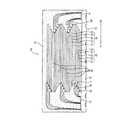
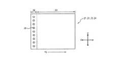
図1は、本発明の一実施形態による積層半導体パッケージの断面図である。図2は、図1に示されている積層半導体パッケージの第1の半導体チップを示した平面図である。Hereinafter, exemplary embodiments of the present invention will be described in detail with reference to the accompanying drawings.
FIG. 1 is a cross-sectional view of a stacked semiconductor package according to an embodiment of the present invention. FIG. 2 is a plan view showing a first semiconductor chip of the stacked semiconductor package shown in FIG.
図1及び図2を参照すると、積層半導体パッケージ100は、基板10と、第1の積層パッケージグループ20と、第1の導電性ワイヤー30と、接着部材40と、第2の積層パッケージグループ50と、第2の導電性ワイヤー60とを含む。 Referring to FIGS. 1 and 2, the
基板10は、平面上から見たとき、直六面体プレート形状を有することができる。基板10は、例えば印刷回路基板でありうる。 The
基板10は、第1の接続パッド12、第2の接続パッド14及びボールランド16を含む。 The
第1の接続パッド12及び第2の接続パッド14は基板10の上面上に配置され、ボールランド16は基板10の上面と対向する下面上に配置される。 The
第1の接続パッド12は基板10の上面の一側エッジに配置され、第2の接続パッド14は基板10の上面の一側エッジと対向する上面の他側エッジに配置される。ボールランド16は第1の接続パッド12及び/又は第2の接続パッド14と電気的に連結される。 The
第1の積層パッケージグループ20は基板10の上面上に付着する。第1の積層パッケージグループ20は複数の第1の半導体チップ21,22,23,24及び隣接した第1の半導体チップ21,22,23,24を接着するための第1の接着部材25を含む。 The first stacked
図2を参照すると、第1の半導体チップ21,22,23,24はチップ領域(CR)及びボンディング領域(BR)を含む。ボンディング領域(BR)はチップ領域(CR)と隣接するように配置される。 Referring to FIG. 2, the
複数のエッジボンディングパッド26はボンディング領域(BR)内に配置される。例えば、エッジボンディングパッド26は図2に示されているY−軸と平行な方向に配置される。 The plurality of
基板10上に付着した第1の積層パッケージグループ20の第1の半導体チップ21,22,23,24の各エッジボンディングパッド26は第1の接続パッド12と隣接するように配置される。 The
隣接した一対の第1の半導体チップ21,22,23,24の間には第1の寸法を有する第1の接着部材25が配置される。第1の接着部材25は、例えば両面接着テープ又は接着剤でありうる。 A first
第1の積層パッケージグループ20の第1の半導体チップ21,22,23,24は第1の方向(FD)に沿って階段形態に積層され、この結果積層された第1の半導体チップ21,22,23,24のボンディング領域(BR)のエッジボンディングパッド26は露出する。 The
第1の導電性ワイヤー30は、相互に隣接するように配置された第1の半導体チップ21,22,23,24の各エッジボンディングパッド26及び基板10の各第1の接続パッド12を電気的に連結する。 The first
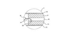
図3は図1のセクションAを示す部分拡大図である。
図1及び図3を参照すると、接着部材40は第1の積層パッケージグループ20の第1の半導体チップ24上に直接配置される。本実施形態で、接着部材40は第1の半導体チップ24と同一な形状及び同一な面積を有し、接着部材40は第1の半導体チップ24のエッジボンディングパッド26と電気的に連結された第1の導電性ワイヤー30のループ部32を覆う。すなわち、接着部材40は第1の導電性ワイヤー30のループ部32を後述する第2の積層パッケージグループ50から絶縁する。FIG. 3 is a partially enlarged view showing section A of FIG.
Referring to FIGS. 1 and 3, the
図1を再び参照すると、第2の積層パッケージグループ50は接着部材40上に付着する。第2の積層パッケージグループ50は複数の第2の半導体チップ51,52,53,54及び第2の接着部材55を含む。 Referring back to FIG. 1, the second
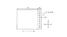
図4は、図1の第2の積層パッケージグループの第2の半導体チップを示した平面図である。 FIG. 4 is a plan view showing a second semiconductor chip of the second stacked package group of FIG.
図4を参照すると、第2の半導体チップ51,52,53,54はチップ領域(CR)及びボンディング領域(BR)を含む。ボンディング領域(BR)はチップ領域(CR)と隣接するように配置され、ボンディング領域(BR)には複数のエッジボンディングパッド56が配置される。例えば、エッジボンディングパッド56は図4に示されているY−軸と平行な方向に配置される。 Referring to FIG. 4, the second semiconductor chips 51, 52, 53, and 54 include a chip region (CR) and a bonding region (BR). The bonding region (BR) is disposed adjacent to the chip region (CR), and a plurality of
第2の積層パッケージグループ50の各第2の半導体チップ51,52,53,54の各エッジボンディングパッド56は、基板10の第2の接続パッド14と隣接するように配置される。本実施形態で、第2の半導体チップ51,52,53,54の形状及びサイズは第1の半導体チップ21,22,23,24と実質的に同一である。 Each
第2の積層パッケージグループ50の第2の半導体チップ51,52,53,54は、例えば第1の方向(FD)とは反対方向である第2の方向(SD)に沿って階段形態に相互に積層されて、第2の半導体チップ51,52,53,54のボンディング領域(BR)のエッジボンディングパッド56は露出する。 For example, the second semiconductor chips 51, 52, 53, and 54 of the second
隣接した第2の半導体チップ51,52,53,54の間には第1の寸法を有する第2の接着部材55が介在する。第2の接着部材55は、例えば第1の寸法を有する両面接着テープ又は接着剤でありうる。 A
本実施形態で、第2の半導体チップ51,52,53,54のうち接着部材40と直接接着した第2の半導体チップ51は第1の積層パッケージグループ20の第1の半導体チップ24と整列する。すなわち、接着部材40の両側にそれぞれ配置された第1の積層パッケージグループ20の第1の半導体チップ24のエッジ及び第2の積層パッケージグループ50の第2の半導体チップ51のエッジは整列する。 In the present embodiment, the
第1の積層パッケージグループ20の第1の半導体チップ24及び第2の積層パッケージグループ50の第2の半導体チップ51が相互に整列する場合、接着部材40及び第1の半導体チップ24が第2の半導体チップ51を支持する。従って、ワイヤーボンディング設備(図示せず)のキャピラリ(図示せず)によって第2の半導体チップ51のエッジボンディングパッド56及び第2の導電性ワイヤー60がワイヤーボンディングされるとき、キャピラリによる第2の半導体チップ51の破損を防止することができる。 When the
これとは異なって、第2の積層パッケージグループ50の第2の半導体チップ51が第1の積層パッケージグループ20の第1の半導体チップ24から突出した状態で第2の半導体チップ51のエッジボンディングパッド56に第2の導電性ワイヤー60がボンディングされる場合、キャピラリによって第2の半導体チップ51の破損が発生できる。 Unlike this, the edge bonding pad of the
第2の導電性ワイヤー60は、基板10の第2の接続パッド14及び第2の接続パッド14と隣接するように配置された第2の半導体チップ51,52,53,54の各エッジボンディングパッド56を電気的に連結する。 The second
本実施形態で、少なくとも2個の第1の積層パッケージグループ20及び第2の積層パッケージグループ50は交互に配置され、これにより積層半導体パッケージ100は約20個の第1及び第2の半導体チップが積層できる。 In the present embodiment, at least two first
モールディング部材70は、基板10上に積層された第1及び第2の積層パッケージグループ20,50、第1及び第2の導電性ワイヤー30,60をモールディングする。モールディング部材70として使用できる物質の例としてはエポキシ樹脂などを挙げることができる。 The
図5及び図6は本発明の一実施形態による積層半導体パッケージの製造方法を示した断面図である。 5 and 6 are cross-sectional views illustrating a method of manufacturing a stacked semiconductor package according to an embodiment of the present invention.
図5を参照すると、積層半導体パッケージを製造するために基板10上には第1の積層パッケージグループ20が配置される。 Referring to FIG. 5, a first
基板10は、平面上から見たとき、直六面体プレート形状を有する。基板10は、例えば第1の接続パッド12、第2の接続パッド14及びボールランド16を有する印刷回路基板でありうる。 The
第1の接続パッド12は基板10の上面の一側エッジに配置され、第2の接続パッド14は基板10の上面の一側エッジと対向する他側エッジに配置される。ボールランド16は、基板10の上面と対向する下面上に配置される。ボールランド16は、第1の接続パッド12及び/又は第2の接続パッド14と電気的に連結される。 The
第1の積層パッケージグループ20を基板10上に形成するために複数の第1の半導体チップ21,22,23,24が設けられる。 In order to form the first
第1の半導体チップ21,22,23,24はそれぞれチップ領域及びボンディング領域を有し、各第1の半導体チップ21,22,23,24のボンディング領域には複数のエッジボンディングパッド26が配置される。 Each of the
第1の半導体チップ21の上面のチップ領域には第1の接着部材25によって他の第1の半導体チップ22の後面が付着し、これにより第1の半導体チップ21のエッジボンディングパッド26は露出する。 The rear surface of the other
次に、他の第1の半導体チップ22の上面のチップ領域には第1の接着部材25によってさらに他の第1の半導体チップ23の後面が付着し、これにより他の半導体チップ22のエッジボンディングパッド26は露出する。 Next, the rear surface of the other
その次に、さらに他の半導体チップ23の上面のチップ領域には第1の接着部材25によって最後の第1の半導体チップ24の後面が付着し、これにより最後の第1の半導体チップ24のエッジボンディングパッド26は露出する。 Next, the rear surface of the last
本実施形態で、第1の接着部材25は第1の寸法を有し、第1の接着部材25は、例えば両面接着テープ又は接着剤でありうる。 In the present embodiment, the first
前述したように第1の半導体チップ21,22,23,24を積層する場合、第1の半導体チップ21,22,23,24は第1の方向(FD)に向かって階段形態に積層される。 As described above, when the
第1の積層パッケージグループ20が基板10上に形成された後、基板10の第1の接続パッド12及び第1の半導体チップ21,22,23,24の各エッジボンディングパッド26は第1の導電性ワイヤー30によって電気的に連結される。 After the first
図6を参照すると、第1の半導体チップ21,22,23,24のエッジボンディングパッド26及び基板10の第1の接続パッド12が第1の導電性ワイヤー30によって電気的に接続された後、第1の積層パッケージグループ20の上部に配置された第1の半導体チップ24上には接着部材40が配置される。 Referring to FIG. 6, after the
接着部材40は、例えば第1の半導体チップ24の上面に塗布された流動性接着剤でありうる。これとは異なって、接着部材40は第1の半導体チップ24の上面に塗布された接着テープでありうる。接着部材40の付着面積は第1の半導体チップ24の面積と実質的に同一であることができる。 The
本実施形態で、接着部材40は第1の半導体チップ24のエッジボンディングパッド26と電気的に連結された第1の導電性ワイヤー30のループ部32を覆う第2の寸法を有する。本実施形態で、接着部材40の第2の寸法は、例えば第1の接着部材25の第1の寸法より厚い寸法を有する。 In the present embodiment, the
第1の半導体チップ24のエッジボンディングパッド26と電気的に連結された第1の導電性ワイヤー30は接着部材40によって後述する第2の積層パッケージグループ50の第2の半導体チップ51と電気的に絶縁される。 The first
第1の積層パッケージグループ20の第1の半導体チップ24上に接着部材40が配置された後、接着部材40上には第2の積層パッケージグループ50が配置される。 After the
第2の積層パッケージグループ50は複数の第2の半導体チップ51,52,53,54を含む。 The second
第2の半導体チップ51,52,53,54はそれぞれチップ領域及びボンディング領域を有し、各第2の半導体チップ51,52,53,54のボンディング領域には複数のエッジボンディングパッド56が配置される。 The second semiconductor chips 51, 52, 53, 54 each have a chip region and a bonding region, and a plurality of
複数の第2の半導体チップ51,52,53,54のうち、第2の半導体チップ51は接着部材40上に直接付着する。 Of the plurality of second semiconductor chips 51, 52, 53, 54, the
この時、第2の積層パッケージグループ50の第2の半導体チップ51は第1の積層パッケージグループ20の第1の半導体チップ24と正確に整列する。 At this time, the
本実施形態で、第2の半導体チップ51が第1の半導体チップ24と正確に整列することによってワイヤーボンディング工程中第2の半導体チップ51の破損を防止することができる。 In the present embodiment, the
第2の半導体チップ51の上面のチップ領域には第2の接着部材55によって他の第2の半導体チップ52の後面が付着し、これにより第2の半導体チップ51のエッジボンディングパッド56は露出する。 The rear surface of the other
次に、他の第2の半導体チップ52の上面のチップ領域には第2の接着部材55によってさらに他の第2の半導体チップ53の後面が付着し、これにより他の半導体チップ52のエッジボンディングパッド56は露出する。 Next, the rear surface of the other
その次に、さらに他の第2の半導体チップ53の上面チップ領域には第2の接着部材55によって最後の第2の半導体チップ54の後面が付着し、これにより最後の第2の半導体チップ54のエッジボンディングパッド56は露出する。 Next, the rear surface of the last
本実施形態で、第2の接着部材55は第1の寸法を有し、第2の接着部材55は、例えば両面接着テープ又は接着剤でありうる。 In the present embodiment, the
前述したように、第2の半導体チップ51,52,53,54を積層する場合、第2の半導体チップ51,52,53,54は第1の方向(FD)とは反対方向である第2の方向(SD)に向かって階段形態に積層される。 As described above, when the second semiconductor chips 51, 52, 53, 54 are stacked, the second semiconductor chips 51, 52, 53, 54 are in the second direction opposite to the first direction (FD). Are stacked in a staircase pattern in the direction (SD).
第2の積層パッケージグループ50が接着部材40上に形成された後、基板10の第2の接続パッド14及び第2の半導体チップ51,52,53,54のエッジボンディングパッド56は第2の導電性ワイヤー60によって電気的に連結される。 After the second
この時、第2の積層パッケージグループ50の第2の半導体チップ51は接着部材40及び第1の積層パッケージグループ20の第1の半導体チップ24によって支持されて、第2の半導体チップ51に第2の導電性ワイヤー60がボンディングされるとき、第2の半導体チップ51の破損を防止することができる。 At this time, the
このような方法で第1及び第2の積層パッケージグループ20、50及び第1及び第2の導電性ワイヤー30,60は多数回交互に配置できる。例えば、本発明による積層半導体パッケージ100は約20個〜約30個の半導体チップを容易に積層することができる。 In this manner, the first and second
図1を再び参照すると、基板10上に第1及び第2の積層パッケージグループ20、50が配置された後、モールディング部材70によって第1及び第2の積層パッケージグループ20,50及び第1及び第2の導電性ワイヤー30,60はモールディングされて積層半導体パッケージ100が製造される。 Referring again to FIG. 1, after the first and second
以上、ここでは本発明を特定実施形態に関連して示して説明したが、本発明はそれに限定されるものでなく、本発明の特許請求の範囲は本発明の精神と分野を離脱しない限度内で本発明が多様に改造及び変形できるということを当業者が容易に分かる。 Although the present invention has been shown and described herein with reference to specific embodiments, the present invention is not limited thereto, and the claims of the present invention are within the limits that do not depart from the spirit and field of the present invention. Those skilled in the art will readily understand that the present invention can be modified and modified in various ways.
10 基板
12 第1の接続パッド
14 第2の接続パッド
16 ボールランド
20 積層パッケージグループ
21,22,23,24 第1の半導体チップ
25 第1の接着部材
30 第1の導電性ワイヤー
40 接着部材
50 第2の積層パッケージグループ
51,52,53,54 第2の半導体チップ
55 第2の接着部材
60 第2の導電性ワイヤー
100 積層半導体パッケージDESCRIPTION OF
Claims (13)
Translated fromJapanese前記基板上に配置され、第1のエッジボンディングパッドが露出した第1の半導体チップが階段形態に積層された第1の積層パッケージグループと、
前記第1のエッジボンディングパッド及び前記第1の接続パッドを電気的に連結する第1の導電性ワイヤーと、
前記第1の積層パッケージグループの上部に配置された第1の上部半導体チップ上に配置された接着部材と、
前記接着部材上に配置され、階段形態に積層されて第2のエッジボンディングパッドが露出して前記第1の上部半導体チップと整列した第2の下部半導体チップを含む第2の半導体チップを含む第2の積層パッケージグループと、
前記第2のエッジボンディングパッド及び前記第2の接続パッドを電気的に連結する第2の導電性ワイヤーと、
を含むことを特徴とする積層半導体パッケージ。A substrate including a first connection pad and a second connection pad;
A first stacked package group in which a first semiconductor chip disposed on the substrate and having a first edge bonding pad exposed is stacked in a staircase configuration;
A first conductive wire that electrically connects the first edge bonding pad and the first connection pad;
An adhesive member disposed on a first upper semiconductor chip disposed above the first stacked package group;
A second semiconductor chip including a second lower semiconductor chip disposed on the adhesive member and including a second lower semiconductor chip aligned with the first upper semiconductor chip, wherein the second edge bonding pads are exposed and stacked in a staircase configuration; Two stacked package groups;
A second conductive wire that electrically connects the second edge bonding pad and the second connection pad;
A laminated semiconductor package comprising:
前記第1のエッジボンディングパッド及び前記第1の接続パッドを第1の導電性ワイヤーで電気的に連結する段階と、
前記第1の積層パッケージグループの第1の上部半導体チップ上に接着部材を形成する段階と、
前記接着部材上に階段形態に積層されて第2のエッジボンディングパッドが露出し、前記第1の上部半導体チップと整列した第2の下部半導体チップを有する第2の半導体チップを含む第2の積層パッケージグループを形成する段階と、
前記第2のエッジボンディングパッド及び前記第2の接続パッドを第2の導電性ワイヤーで電気的に連結する段階と、
を含むことを特徴とする積層半導体パッケージの製造方法。Stacking a first semiconductor chip having a first edge bonding pad exposed on a substrate including a first connection pad and a second connection pad in a staircase configuration to form a first stacked package group;
Electrically connecting the first edge bonding pad and the first connection pad with a first conductive wire;
Forming an adhesive member on the first upper semiconductor chip of the first stacked package group;
A second stack including a second semiconductor chip having a second lower semiconductor chip aligned with the first upper semiconductor chip, wherein the second edge bonding pads are exposed in a stepped configuration on the adhesive member. Forming a package group;
Electrically connecting the second edge bonding pad and the second connection pad with a second conductive wire;
A method for manufacturing a stacked semiconductor package, comprising:
Applications Claiming Priority (1)
| Application Number | Priority Date | Filing Date | Title |
|---|---|---|---|
| KR1020070103880AKR100886717B1 (en) | 2007-10-16 | 2007-10-16 | Laminated semiconductor package and method for manufacturing same |
Publications (1)
| Publication Number | Publication Date |
|---|---|
| JP2009099922Atrue JP2009099922A (en) | 2009-05-07 |
Family
ID=40533378
Family Applications (1)
| Application Number | Title | Priority Date | Filing Date |
|---|---|---|---|
| JP2007311666APendingJP2009099922A (en) | 2007-10-16 | 2007-11-30 | Multilayer semiconductor package and manufacturing method thereof |
Country Status (5)
| Country | Link |
|---|---|
| US (1) | US7705468B2 (en) |
| JP (1) | JP2009099922A (en) |
| KR (1) | KR100886717B1 (en) |
| CN (1) | CN101414603B (en) |
| TW (1) | TWI351752B (en) |
Cited By (2)
| Publication number | Priority date | Publication date | Assignee | Title |
|---|---|---|---|---|
| JP2009158739A (en)* | 2007-12-27 | 2009-07-16 | Toshiba Corp | Semiconductor device and semiconductor memory device |
| JP2013522887A (en)* | 2010-03-18 | 2013-06-13 | モサイド・テクノロジーズ・インコーポレーテッド | Multi-chip package using offset die stacking and its fabrication method |
Families Citing this family (17)
| Publication number | Priority date | Publication date | Assignee | Title |
|---|---|---|---|---|
| KR101539402B1 (en)* | 2008-10-23 | 2015-07-27 | 삼성전자주식회사 | Semiconductor Package |
| JP4776675B2 (en) | 2008-10-31 | 2011-09-21 | 株式会社東芝 | Semiconductor memory card |
| KR20100049283A (en)* | 2008-11-03 | 2010-05-12 | 삼성전자주식회사 | Semiconductor package and method for manufacturing of the same |
| KR101563630B1 (en)* | 2009-09-17 | 2015-10-28 | 에스케이하이닉스 주식회사 | Semiconductor package |
| KR101640832B1 (en)* | 2010-07-16 | 2016-07-19 | 삼성전자주식회사 | stacked Semiconductor Package and Method of fabricating the same |
| KR20120035297A (en) | 2010-10-05 | 2012-04-16 | 삼성전자주식회사 | Semiconductor package and method of manufacturing the semiconductor package |
| US20130037952A1 (en)* | 2011-08-09 | 2013-02-14 | SK Hynix Inc. | Semiconductor package and method for manufacturing the same |
| KR20140081544A (en) | 2012-12-21 | 2014-07-01 | 에스케이하이닉스 주식회사 | semiconductor chip having protrusion, stacked package of the same and method of fabricating stacked package |
| US9230942B2 (en)* | 2013-02-26 | 2016-01-05 | Sandisk Information Technology (Shanghai) Co., Ltd. | Semiconductor device including alternating stepped semiconductor die stacks |
| KR102576764B1 (en)* | 2016-10-28 | 2023-09-12 | 에스케이하이닉스 주식회사 | Semiconductor packages of asymmetric chip stacks |
| KR102671937B1 (en)* | 2017-01-10 | 2024-06-05 | 에스케이하이닉스 주식회사 | Nonvolatile memory device including multi plane |
| CN109755182A (en)* | 2017-11-07 | 2019-05-14 | 中芯国际集成电路制造(上海)有限公司 | Chip stack package structure and forming method thereof |
| JP2019161095A (en)* | 2018-03-15 | 2019-09-19 | 東芝メモリ株式会社 | Semiconductor device |
| CN111348613B (en)* | 2018-12-21 | 2023-12-26 | 中芯集成电路(宁波)有限公司 | Packaging method and packaging structure |
| US10978419B1 (en)* | 2019-10-14 | 2021-04-13 | Nanya Technology Corporation | Semiconductor package and manufacturing method thereof |
| KR20220015066A (en)* | 2020-07-30 | 2022-02-08 | 삼성전자주식회사 | Multi-chip package |
| JP7699416B2 (en)* | 2021-12-10 | 2025-06-27 | キオクシア株式会社 | Semiconductor Device |
Citations (12)
| Publication number | Priority date | Publication date | Assignee | Title |
|---|---|---|---|---|
| JPH08288455A (en)* | 1995-04-11 | 1996-11-01 | Oki Electric Ind Co Ltd | Semiconductor device and its manufacture |
| JPH1027880A (en)* | 1996-07-09 | 1998-01-27 | Sumitomo Metal Mining Co Ltd | Semiconductor device |
| JP2001298150A (en)* | 2000-04-14 | 2001-10-26 | Hitachi Ltd | Semiconductor device and manufacturing method thereof |
| JP2001308262A (en)* | 2000-04-26 | 2001-11-02 | Mitsubishi Electric Corp | Resin-sealed BGA type semiconductor device |
| JP2002222913A (en)* | 2001-01-24 | 2002-08-09 | Sharp Corp | Semiconductor device and method of manufacturing the same |
| JP2004072009A (en)* | 2002-08-09 | 2004-03-04 | Fujitsu Ltd | Semiconductor device and manufacturing method thereof |
| JP2004296897A (en)* | 2003-03-27 | 2004-10-21 | Seiko Epson Corp | Semiconductor device, electronic device, electronic apparatus, and method of manufacturing semiconductor device |
| JP2006313798A (en)* | 2005-05-06 | 2006-11-16 | Oki Electric Ind Co Ltd | Semiconductor device and manufacturing method thereof |
| JP2007035865A (en)* | 2005-07-26 | 2007-02-08 | Toshiba Corp | Semiconductor package and manufacturing method thereof |
| JP2007242684A (en)* | 2006-03-06 | 2007-09-20 | Disco Abrasive Syst Ltd | Stacked semiconductor device and device stacking method |
| JP2008160119A (en)* | 2006-12-20 | 2008-07-10 | Stats Chippac Ltd | Integrated circuit package system |
| JP2009049118A (en)* | 2007-08-17 | 2009-03-05 | Toshiba Corp | Semiconductor device and semiconductor package using the same |
Family Cites Families (21)
| Publication number | Priority date | Publication date | Assignee | Title |
|---|---|---|---|---|
| US5864177A (en)* | 1996-12-12 | 1999-01-26 | Honeywell Inc. | Bypass capacitors for chip and wire circuit assembly |
| US5987357A (en)* | 1997-07-30 | 1999-11-16 | Intermedics Inc. | Stackable microelectronic components with self-addressing scheme |
| US6252305B1 (en)* | 2000-02-29 | 2001-06-26 | Advanced Semiconductor Engineering, Inc. | Multichip module having a stacked chip arrangement |
| US6900528B2 (en)* | 2001-06-21 | 2005-05-31 | Micron Technology, Inc. | Stacked mass storage flash memory package |
| JP2007066922A (en)* | 2003-11-28 | 2007-03-15 | Renesas Technology Corp | Semiconductor integrated circuit device |
| JP4406300B2 (en)* | 2004-02-13 | 2010-01-27 | 株式会社東芝 | Semiconductor device and manufacturing method thereof |
| DE102004049356B4 (en)* | 2004-10-08 | 2006-06-29 | Infineon Technologies Ag | Semiconductor module with an internal semiconductor chip stack and method for producing the same |
| US20060267173A1 (en)* | 2005-05-26 | 2006-11-30 | Sandisk Corporation | Integrated circuit package having stacked integrated circuits and method therefor |
| US7402911B2 (en)* | 2005-06-28 | 2008-07-22 | Infineon Technologies Ag | Multi-chip device and method for producing a multi-chip device |
| JP2007134486A (en)* | 2005-11-10 | 2007-05-31 | Toshiba Corp | Multilayer semiconductor device and manufacturing method thereof |
| JP2007294488A (en)* | 2006-04-20 | 2007-11-08 | Shinko Electric Ind Co Ltd | Semiconductor device, process for manufacturing the same and electronic component |
| KR100842907B1 (en)* | 2006-09-07 | 2008-07-02 | 주식회사 하이닉스반도체 | Multi-chip package |
| TWI358815B (en)* | 2006-09-12 | 2012-02-21 | Chipmos Technologies Inc | Stacked chip package structure with lead-frame hav |
| US8138591B2 (en)* | 2006-09-23 | 2012-03-20 | Stats Chippac Ltd | Integrated circuit package system with stacked die |
| US7408245B2 (en)* | 2006-12-22 | 2008-08-05 | Powertech Technology Inc. | IC package encapsulating a chip under asymmetric single-side leads |
| US7875985B2 (en)* | 2006-12-22 | 2011-01-25 | Qimonda Ag | Memory device |
| US7880309B2 (en)* | 2007-07-30 | 2011-02-01 | Qimonda Ag | Arrangement of stacked integrated circuit dice having a direct electrical connection |
| US7906853B2 (en)* | 2007-09-06 | 2011-03-15 | Micron Technology, Inc. | Package structure for multiple die stack |
| JP4498403B2 (en)* | 2007-09-28 | 2010-07-07 | 株式会社東芝 | Semiconductor device and semiconductor memory device |
| US7952183B2 (en)* | 2007-10-29 | 2011-05-31 | Kabushiki Kaisha Toshiba | High capacity memory with stacked layers |
| US7687921B2 (en)* | 2008-05-05 | 2010-03-30 | Super Talent Electronics, Inc. | High density memory device manufacturing using isolated step pads |
- 2007
- 2007-10-16KRKR1020070103880Apatent/KR100886717B1/enactiveActive
- 2007-11-15USUS11/940,522patent/US7705468B2/enactiveActive
- 2007-11-21TWTW096144029Apatent/TWI351752B/enactive
- 2007-11-30JPJP2007311666Apatent/JP2009099922A/enactivePending
- 2008
- 2008-01-04CNCN2008100016127Apatent/CN101414603B/enactiveActive
Patent Citations (12)
| Publication number | Priority date | Publication date | Assignee | Title |
|---|---|---|---|---|
| JPH08288455A (en)* | 1995-04-11 | 1996-11-01 | Oki Electric Ind Co Ltd | Semiconductor device and its manufacture |
| JPH1027880A (en)* | 1996-07-09 | 1998-01-27 | Sumitomo Metal Mining Co Ltd | Semiconductor device |
| JP2001298150A (en)* | 2000-04-14 | 2001-10-26 | Hitachi Ltd | Semiconductor device and manufacturing method thereof |
| JP2001308262A (en)* | 2000-04-26 | 2001-11-02 | Mitsubishi Electric Corp | Resin-sealed BGA type semiconductor device |
| JP2002222913A (en)* | 2001-01-24 | 2002-08-09 | Sharp Corp | Semiconductor device and method of manufacturing the same |
| JP2004072009A (en)* | 2002-08-09 | 2004-03-04 | Fujitsu Ltd | Semiconductor device and manufacturing method thereof |
| JP2004296897A (en)* | 2003-03-27 | 2004-10-21 | Seiko Epson Corp | Semiconductor device, electronic device, electronic apparatus, and method of manufacturing semiconductor device |
| JP2006313798A (en)* | 2005-05-06 | 2006-11-16 | Oki Electric Ind Co Ltd | Semiconductor device and manufacturing method thereof |
| JP2007035865A (en)* | 2005-07-26 | 2007-02-08 | Toshiba Corp | Semiconductor package and manufacturing method thereof |
| JP2007242684A (en)* | 2006-03-06 | 2007-09-20 | Disco Abrasive Syst Ltd | Stacked semiconductor device and device stacking method |
| JP2008160119A (en)* | 2006-12-20 | 2008-07-10 | Stats Chippac Ltd | Integrated circuit package system |
| JP2009049118A (en)* | 2007-08-17 | 2009-03-05 | Toshiba Corp | Semiconductor device and semiconductor package using the same |
Cited By (3)
| Publication number | Priority date | Publication date | Assignee | Title |
|---|---|---|---|---|
| JP2009158739A (en)* | 2007-12-27 | 2009-07-16 | Toshiba Corp | Semiconductor device and semiconductor memory device |
| JP2013522887A (en)* | 2010-03-18 | 2013-06-13 | モサイド・テクノロジーズ・インコーポレーテッド | Multi-chip package using offset die stacking and its fabrication method |
| US9177863B2 (en) | 2010-03-18 | 2015-11-03 | Conversant Intellectual Property Management Inc. | Multi-chip package with offset die stacking and method of making same |
Also Published As
| Publication number | Publication date |
|---|---|
| KR100886717B1 (en) | 2009-03-04 |
| CN101414603B (en) | 2012-04-18 |
| US20090096075A1 (en) | 2009-04-16 |
| TWI351752B (en) | 2011-11-01 |
| TW200919693A (en) | 2009-05-01 |
| US7705468B2 (en) | 2010-04-27 |
| CN101414603A (en) | 2009-04-22 |
Similar Documents
| Publication | Publication Date | Title |
|---|---|---|
| JP2009099922A (en) | Multilayer semiconductor package and manufacturing method thereof | |
| JP4808408B2 (en) | Multi-chip package, semiconductor device used for the same, and manufacturing method thereof | |
| KR102247916B1 (en) | Semiconductro pacakages having stepwised stacking structures | |
| TWI481001B (en) | Chip packaging structure and manufacturing method for the same | |
| US20120146216A1 (en) | Semiconductor package and fabrication method thereof | |
| JP2003078106A (en) | Chip stacked package element and method of manufacturing the same | |
| KR20150012285A (en) | Substrate-less stackable package with wire-bond interconnect | |
| JP2009044110A (en) | Semiconductor device and its manufacturing method | |
| US20110084374A1 (en) | Semiconductor package with sectioned bonding wire scheme | |
| CN101477980A (en) | Stacked wafer level package with reduced size | |
| KR101123804B1 (en) | Semiconductor chip and stacked semiconductor package havng the same | |
| US7042104B2 (en) | Semiconductor package using flexible film and method of manufacturing the same | |
| US20070045864A1 (en) | Semiconductor device including a plurality of semiconductor chips stacked three-dimensionally, and method of manufacturing the same | |
| US7638365B2 (en) | Stacked chip package and method for forming the same | |
| KR20110138788A (en) | Stacked Semiconductor Packages | |
| US7224055B2 (en) | Center pad type IC chip with jumpers, method of processing the same and multi chip package | |
| CN103219244B (en) | System-in-package structure for semiconductor package | |
| KR20040069392A (en) | Stacked type semiconductor multichip package | |
| KR100988403B1 (en) | Semiconductor package and wafer level semiconductor package manufacturing method | |
| KR20110050028A (en) | Printed circuit board and semiconductor package including the same | |
| KR20090079401A (en) | Semiconductor Package Device Having Redistribution Layer | |
| KR20010025861A (en) | Stack type chip scale semiconductor package | |
| KR100876896B1 (en) | Laminated Semiconductor Packages | |
| KR20110107125A (en) | Semiconductor package | |
| KR20110105165A (en) | Interposer and Stack Package With It |
Legal Events
| Date | Code | Title | Description |
|---|---|---|---|
| A621 | Written request for application examination | Free format text:JAPANESE INTERMEDIATE CODE: A621 Effective date:20101014 | |
| A977 | Report on retrieval | Free format text:JAPANESE INTERMEDIATE CODE: A971007 Effective date:20120222 | |
| RD01 | Notification of change of attorney | Free format text:JAPANESE INTERMEDIATE CODE: A7421 Effective date:20120227 | |
| A131 | Notification of reasons for refusal | Free format text:JAPANESE INTERMEDIATE CODE: A131 Effective date:20120228 | |
| RD03 | Notification of appointment of power of attorney | Free format text:JAPANESE INTERMEDIATE CODE: A7423 Effective date:20120418 | |
| A521 | Request for written amendment filed | Free format text:JAPANESE INTERMEDIATE CODE: A523 Effective date:20120528 | |
| A02 | Decision of refusal | Free format text:JAPANESE INTERMEDIATE CODE: A02 Effective date:20121009 |