JP2009094576A - Signal transfer circuit - Google Patents
Signal transfer circuitDownload PDFInfo
- Publication number
- JP2009094576A JP2009094576AJP2007260309AJP2007260309AJP2009094576AJP 2009094576 AJP2009094576 AJP 2009094576AJP 2007260309 AJP2007260309 AJP 2007260309AJP 2007260309 AJP2007260309 AJP 2007260309AJP 2009094576 AJP2009094576 AJP 2009094576A
- Authority
- JP
- Japan
- Prior art keywords
- voltage
- switching element
- power supply
- coil
- circuit
- Prior art date
- Legal status (The legal status is an assumption and is not a legal conclusion. Google has not performed a legal analysis and makes no representation as to the accuracy of the status listed.)
- Granted
Links
- 230000008054signal transmissionEffects0.000claimsdescription134
- 230000000630rising effectEffects0.000claimsdescription51
- 230000002159abnormal effectEffects0.000claimsdescription19
- 230000005856abnormalityEffects0.000claimsdescription5
- 230000008878couplingEffects0.000abstractdescription14
- 238000010168coupling processMethods0.000abstractdescription14
- 238000005859coupling reactionMethods0.000abstractdescription14
- 238000010586diagramMethods0.000description22
- 230000007257malfunctionEffects0.000description14
- 230000010355oscillationEffects0.000description12
- 230000003111delayed effectEffects0.000description8
- 239000000872bufferSubstances0.000description6
- 230000005540biological transmissionEffects0.000description3
- 230000007423decreaseEffects0.000description3
- 238000000034methodMethods0.000description2
Images


Classifications
- H—ELECTRICITY
- H04—ELECTRIC COMMUNICATION TECHNIQUE
- H04L—TRANSMISSION OF DIGITAL INFORMATION, e.g. TELEGRAPHIC COMMUNICATION
- H04L25/00—Baseband systems
- H04L25/02—Details ; arrangements for supplying electrical power along data transmission lines
- H04L25/0264—Arrangements for coupling to transmission lines
- H04L25/0266—Arrangements for providing Galvanic isolation, e.g. by means of magnetic or capacitive coupling
- H—ELECTRICITY
- H03—ELECTRONIC CIRCUITRY
- H03K—PULSE TECHNIQUE
- H03K17/00—Electronic switching or gating, i.e. not by contact-making and –breaking
- H03K17/08—Modifications for protecting switching circuit against overcurrent or overvoltage
- H03K17/081—Modifications for protecting switching circuit against overcurrent or overvoltage without feedback from the output circuit to the control circuit
- H03K17/0814—Modifications for protecting switching circuit against overcurrent or overvoltage without feedback from the output circuit to the control circuit by measures taken in the output circuit
- H03K17/08142—Modifications for protecting switching circuit against overcurrent or overvoltage without feedback from the output circuit to the control circuit by measures taken in the output circuit in field-effect transistor switches
- H—ELECTRICITY
- H03—ELECTRONIC CIRCUITRY
- H03K—PULSE TECHNIQUE
- H03K17/00—Electronic switching or gating, i.e. not by contact-making and –breaking
- H03K17/16—Modifications for eliminating interference voltages or currents
- H03K17/161—Modifications for eliminating interference voltages or currents in field-effect transistor switches
- H03K17/165—Modifications for eliminating interference voltages or currents in field-effect transistor switches by feedback from the output circuit to the control circuit
- H—ELECTRICITY
- H03—ELECTRONIC CIRCUITRY
- H03K—PULSE TECHNIQUE
- H03K17/00—Electronic switching or gating, i.e. not by contact-making and –breaking
- H03K17/51—Electronic switching or gating, i.e. not by contact-making and –breaking characterised by the components used
- H03K17/56—Electronic switching or gating, i.e. not by contact-making and –breaking characterised by the components used by the use, as active elements, of semiconductor devices
- H03K17/687—Electronic switching or gating, i.e. not by contact-making and –breaking characterised by the components used by the use, as active elements, of semiconductor devices the devices being field-effect transistors
- H—ELECTRICITY
- H04—ELECTRIC COMMUNICATION TECHNIQUE
- H04L—TRANSMISSION OF DIGITAL INFORMATION, e.g. TELEGRAPHIC COMMUNICATION
- H04L25/00—Baseband systems
- H04L25/02—Details ; arrangements for supplying electrical power along data transmission lines
- H04L25/0264—Arrangements for coupling to transmission lines
- H04L25/028—Arrangements specific to the transmitter end
- H—ELECTRICITY
- H03—ELECTRONIC CIRCUITRY
- H03K—PULSE TECHNIQUE
- H03K2217/00—Indexing scheme related to electronic switching or gating, i.e. not by contact-making or -breaking covered by H03K17/00
- H03K2217/0045—Full bridges, determining the direction of the current through the load
Landscapes
- Engineering & Computer Science (AREA)
- Power Engineering (AREA)
- Computer Networks & Wireless Communication (AREA)
- Signal Processing (AREA)
- Electronic Switches (AREA)
- Logic Circuits (AREA)
- Dc Digital Transmission (AREA)
- Dc-Dc Converters (AREA)
Abstract
Description
Translated fromJapanese本発明は、入力側と出力側とを電気的に絶縁した状態で、デジタル信号を入力側から出力側に伝達する信号伝達回路に関する。 The present invention relates to a signal transmission circuit that transmits a digital signal from an input side to an output side in a state where the input side and the output side are electrically insulated.
信号伝達回路として、入力側と出力側とを電気的に絶縁状態にする部分にフォトカプラを用いるものがある。
しかしながら、フォトカプラは入出力間の伝送遅延が大きいため、上述の信号伝達回路では、デジタル信号の伝送遅延が大きくなってしまうという問題がある。また、フォトカプラは、100℃以上の環境下で使用できないため、上述の信号伝達回路では、100℃以上の環境下で使用できないという問題もある。Some signal transmission circuits use a photocoupler in a portion where the input side and the output side are electrically insulated.
However, since the photocoupler has a large transmission delay between input and output, the above-described signal transmission circuit has a problem that the transmission delay of the digital signal becomes large. Further, since the photocoupler cannot be used in an environment of 100 ° C. or higher, there is a problem that the above-described signal transmission circuit cannot be used in an environment of 100 ° C. or higher.
これらの問題を解決するために、例えば、入力側と出力側とを電気的に絶縁状態にする部分にフォトカプラの代わりにトランスを用いることが考えられる。
図20は、入力側と出力側とを電気的に絶縁状態にする部分としてトランスを用いた信号伝達回路を示す図である。In order to solve these problems, for example, it is conceivable to use a transformer instead of a photocoupler in a portion where the input side and the output side are electrically insulated.
FIG. 20 is a diagram showing a signal transmission circuit using a transformer as a part for electrically insulating the input side and the output side.
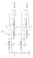
図20に示す信号伝達回路190は、デジタル信号(入力信号)が入力される1次側回路191と、デジタル信号(出力信号)を出力する2次側回路192と、1次側回路191から2次側回路192へデジタル信号を電気的に絶縁して伝達するトランス193とを備えて構成されている。 20 includes a primary circuit 191 to which a digital signal (input signal) is input, a secondary circuit 192 that outputs a digital signal (output signal), and primary circuit 191 to 2. And a
上記トランス193は、1次側コイルと2次側コイルとを備えている。
上記1次側回路191は、電源部194、195と、駆動回路196とを備えて構成されている。The
The primary circuit 191 includes
上記電源部194、195は、それぞれ、nチャネルのMOSFET197と、pチャネルのMOSFET198と、ダイオード199、200とを備えて構成されている。
MOSFET198のソース端子は電圧VDDの電源及びダイオード199のカソード端子に接続され、MOSFET198のドレイン端子はMOSFET197のドレイン端子、ダイオード199のアノード端子、及びダイオード200のカソード端子に接続されている。MOSFET197のソース端子及びダイオード200のアノード端子はそれぞれグランドに接続されている。電源部194においてMOSFET197、198の接続点はトランス193の1次側コイルの一方端に接続され、電源部195においてMOSFET197、198の接続点はトランス193の1次側コイルの他方端に接続されている。Each of the
The source terminal of
なお、トランス193の1次側コイルの一方端(電源部194に接続される点)をA点とし、トランス193の1次側コイルの他方端(電源部195に接続される点)をB点とする。 Note that one end of the primary coil of the transformer 193 (point connected to the power supply unit 194) is point A, and the other end of the primary coil of the transformer 193 (point connected to the power source unit 195) is point B. And
上記2次側回路192は、抵抗201と、コンパレータ(ヒステリシスコンパレータ)202、203と、フリップフロップ回路204とを備えて構成されている。
コンパレータ202のプラスの入力端子はトランス193の2次側コイルの一方端、抵抗201の一方端、及びコンパレータ203のマイナスの入力端子に接続され、コンパレータ202の出力端子はフリップフロップ回路204のセット端子(S)に接続されている。The secondary side circuit 192 includes a
The positive input terminal of the
コンパレータ203のプラスの入力端子はトランス193の2次側コイルの他方端、抵抗201の他方端、及びコンパレータ202のマイナスの入力端子に接続され、コンパレータ203の出力端子はフリップフロップ回路204のリセット端子(R)に接続されている。 The positive input terminal of the
なお、トランス193の2次側コイルの一方端(コンパレータ202のプラスの入力端子に接続される点)をC点とし、トランス193の2次側コイルの他方端(コンパレータ203のプラスの入力端子に接続される点)をD点とする。 Note that one end of the secondary side coil of the transformer 193 (point connected to the positive input terminal of the comparator 202) is C point, and the other end of the secondary side coil of the transformer 193 (to the positive input terminal of the comparator 203). Let D be a point that is connected).
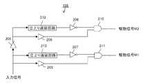
図21は、駆動回路196を示す図である。
図21に示す駆動回路196は、インバータ205〜207と、バッファ208、209と、AND回路210、211と、立上り遅延回路212、213とを備えて構成されている。FIG. 21 is a diagram showing the
The
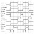
図22は、駆動回路196内の各回路の出力タイミングチャートを示す図である。
立上りタイミング時の入力信号は、バッファ209を介してAND回路211の一方の入力端子に入力されると共に、立上り遅延回路213により所定時間遅延され、インバータ207により反転され、AND回路211の他方の入力端子に入力される。これにより、AND回路211は、入力信号の立上りタイミングにおいてハイレベルのパルス電圧を出力する。AND回路211から出力されるハイレベルのパルス電圧は電源部195のMOSFET197、198のそれぞれのゲート端子に駆動信号M1として入力される。また、このとき、AND回路210から出力されるローレベルの電圧は電源部194のMOSFET197、198のそれぞれのゲート端子に駆動信号M2として入力される。FIG. 22 is a diagram illustrating an output timing chart of each circuit in the
An input signal at the rising timing is input to one input terminal of the
すると、電源部194のMOSFET198と電源部195のMOSFET197がON、電源部194のMOSFET197と電源部195のMOSFET、198がOFFになり、1次側回路191のB点がグランドに繋がるため、B点の電圧がローレベル(V=0)となり、1次側回路191のA点の電圧がハイレベル(V=+VDD)となる。 Then, the
したがって、1次側回路191のA点−B点間にプラス極性のパルス電圧が発生し、トランス193を介して2次側回路192のC点−D点間にプラス極性のパルス電圧が発生する。そして、コンパレータ202から出力されるハイレベルのパルス電圧がフリップフロップ回路204のセット端子(S)に入力され、フリップフロップ回路204の出力端子(Q)から出力される電圧(出力信号)が立ち上がる。 Accordingly, a positive polarity pulse voltage is generated between the points A and B of the primary side circuit 191, and a positive polarity pulse voltage is generated between the points C and D of the secondary side circuit 192 via the
また、立下りタイミング時の入力信号は、インバータ205により反転され、アンプ208を介してAND回路210の一方の入力端子に入力されると共に、インバータ205により反転され、立上り遅延回路212により所定時間遅延され、インバータ206により反転され、AND回路210の他方の入力端子に入力される。これにより、AND回路210は、入力信号の立下りタイミングにおいてハイレベルのパルス電圧を出力する。AND回路210から出力されるハイレベルのパルス電圧は電源部194のMOSFET197、198のそれぞれのゲート端子に駆動信号M1として入力される。また、AND回路211から出力されるローレベルの電圧は電源部195のMOSFET197、198のそれぞれのゲート端子に駆動信号M2として入力される。すると、電源部194のMO
SFET197と電源部195のMOSFET198がON、電源部194のMOSFET198と電源部195のMOSFET197がOFFになり、1次側回路191のA点がグランドに繋がるため、A点の電圧がローレベルとなり、1次側回路191のB点の電圧がハイレベルとなる。The input signal at the falling timing is inverted by the
Since the SFET 197 and the
したがって、1次側回路191のA点−B点間にマイナス極性のパルス電圧が発生し、トランス193を介して2次側回路192のC点−D点間にマイナス極性のパルス電圧が発生する。そして、コンパレータ203から出力されるハイレベルのパルス電圧がフリップフロップ回路204のリセット端子(R)に入力され、フリップフロップ回路204の出力端子(Q)から出力される電圧(出力信号)が立ち下がる。 Accordingly, a negative polarity pulse voltage is generated between the points A and B of the primary side circuit 191, and a negative polarity pulse voltage is generated between the points C and D of the secondary side circuit 192 via the
このように、図20に示す信号伝達回路190によれば、入力信号の立上りタイミングにおいてフリップフロップ回路204から出力される電圧が立ち上がり、入力信号の立下りタイミングにおいてフリップフロップ回路204から出力される電圧が立ち下がる。すなわち、1次側回路191に入力される入力信号の立上りタイミング及び立下りタイミングと同じ立上りタイミング及び立下りタイミングの出力信号が2次側回路192から出力される。図20に示す信号伝達回路190によれば、トランス193により1次側回路191と2次側回路192とを電気的に絶縁して入力信号を1次側回路191から2次側回路192へ伝達することができる。 As described above, according to the
しかしながら、図20に示す信号伝達回路190では、2次側回路192のC点やD点に容量成分などが付き、かつ、トランス193の結合係数が悪いと、誤動作するという問題がある。 However, the
図23は、信号伝達回路190が誤動作する場合の信号伝達回路190内の各回路の出力タイミングチャートを示す図である。
入力信号の立上りタイミングにおいて、電源部195のMOSFET197、198のそれぞれのゲート端子にハイレベルのパルス電圧が入力され、電源部194のMOSFET197、198のそれぞれのゲート端子にローレベルの電圧が入力されると、図23に示すように、1次側回路191のA点の電圧がハイレベル(V=+VDD)、B点の電圧
がローレベル(V=0)となる。したがって、1次側回路61のA点−B点間にプラス極性のパルス電圧が発生し、トランス63を介して、2次側回路192のC点-D点間にA点―B点間に発生したプラス極性の電圧に対応するプラス極性のパルス電圧が発生する。このとき、トランス193の結合係数が悪いと、トランス193のリーケージインダクタンスとC、D点の容量成分とによりLC発振回路が形成され、このLC発振回路が発振することにより、C−D点間の電圧がD点の電圧よりC点の電圧が高いマイナス極性の電圧になってしまう。このような場合、コンパレータ203からハイレベルのパルス電圧が出力されてフリップフロップ回路204の出力電圧がハイレベルからローレベルになり、入力信号と出力信号とが一致しなくなる場合がある。FIG. 23 is a diagram illustrating an output timing chart of each circuit in the
At the rising timing of the input signal, a high-level pulse voltage is input to the gate terminals of the
また、入力信号の立下りタイミングにおいて、電源部194のMOSFET197、198のそれぞれのゲート端子にハイレベルのパルス電圧が入力され、電源部195のMOSFET197、198のそれぞれのゲート端子にローレベルの電圧が入力されると、図23に示すように、1次側回路191のA点の電圧がローレベル、B点の電圧がハイレベルとなる。したがって、1次側回路61のA点−B点間にマイナス極性のパルス電圧が発生し、トランス63を介して、2次側回路192のC点-D点間にA点―B点間に発生したマイナス極性の電圧に対応するマイナス極性のパルス電圧が発生する。このとき、トランス193の結合係数が悪いと、上述と同様に、トランス193のリーケージインダクタンスとC点、D点の容量成分とによりLC発振回路が形成され、このLC発振回路が発振することより、C点−D点の電圧がC点の電圧よりD点の電圧が高いプラス極性の電圧になってしまう。このような場合、コンパレータ202からハイレベルのパルス電圧が出力されてフリップフロップ回路204の出力電圧がローレベルからハイレベルになり、入力信号と出力信号とが一致しなくなる場合がある。 Further, at the falling timing of the input signal, a high level pulse voltage is input to the respective gate terminals of the
このように、図20に示す信号伝達回路190では、トランス193の結合係数が悪いと、誤動作するおそれがある。
ところで、トランスを介して1次側から2次側にデジタル信号を伝える信号伝達方式において、入力されるデジタル信号のハイレベル期間中、プラス極性及びマイナス極性のパルス信号をトランスの1次側コイルに交互に印加し続けてトランスに蓄積されたエネルギーを相殺するものがある。(例えば、特許文献1参照)
そこで、図20に示す信号伝達回路190において、トランス193の2次側回路において発振することを防止するために、上述の信号伝達方式を信号伝達回路190に適用することが考えられる。
By the way, in the signal transmission method for transmitting a digital signal from the primary side to the secondary side through the transformer, pulse signals of plus polarity and minus polarity are transmitted to the primary side coil of the transformer during the high level period of the input digital signal. There is one that cancels the energy accumulated in the transformer by continuing to apply alternately. (For example, see Patent Document 1)
Therefore, in the
しかしながら、入力信号の立上りタイミング及び立下りタイミング以外のタイミングにおいて、トランス193の2次側コイルに発生するプラス極性またはマイナス極性のパルス信号によりコンパレータ202、203からハイレベルのパルス電圧が出力してしまうため、入力されるデジタル信号と異なる立上りタイミング及び立下りタイミングのデジタル信号が2次側回路192から出力されてしまうという問題がある。 However, at a timing other than the rising timing and falling timing of the input signal, a high-level pulse voltage is output from the
そこで、本発明では、入力側と出力側とを電気的に絶縁状態にする部分にトランスを用いる場合において、そのトランスの結合係数が悪くても誤動作を抑えることが可能な信号伝達回路を提供することを目的とする。 Therefore, the present invention provides a signal transmission circuit capable of suppressing malfunction even when a transformer is used in a portion where the input side and the output side are electrically insulated from each other even if the coupling coefficient of the transformer is poor. For the purpose.
上記の課題を解決するために本発明では、以下のような構成を採用した。
すなわち、本発明の信号伝達回路は、1次側コイルと2次側コイルとを有するトランスと、電源とグランドとの間に設けられる複数のスイッチング素子と、入力信号の立上りタイミングにおいて、前記複数のスイッチング素子をそれぞれ制御することにより、前記1次側コイルに第1の極性の電圧を発生させ、前記入力信号の立下りタイミングにおいて、前記複数のスイッチング素子をそれぞれ制御することにより、前記1次側コイルに前記第1の極性と逆極性の第2の極性の電圧を発生させる駆動回路と、前記2次側コイルに第1の閾値以上の前記第1の極性の電圧が発生すると、出力信号を立ち上がらせ、前記2次側コイルに第2の閾値以上の前記第2の極性の電圧が発生すると、前記出力信号を立ち下がらせる2次側回路とを有する信号伝達回路であって、前記駆動回路は、前記2次側コイルに前記第1の閾値以上の前記第1の極性の電圧が発生した後、前記2次側コイルに前記第2の閾値未満の前記第2の極性の電圧を発生させる電圧を前記1次側コイルに発生させるように前記スイッチング素子を制御し、前記1次側コイルに前記第2の閾値以上の前記第2の極性の電圧が発生した後、前記2次側コイルに前記第1の閾値未満の前記第1の極性の電圧を発生させる電圧を前記1次側コイルに発生させるように前記スイッチング素子を制御する。In order to solve the above problems, the present invention adopts the following configuration.
That is, the signal transmission circuit of the present invention includes a transformer having a primary side coil and a secondary side coil, a plurality of switching elements provided between a power source and a ground, and a plurality of the plurality of switching elements at a rising timing of an input signal. By controlling each of the switching elements, a voltage having a first polarity is generated in the primary side coil, and each of the plurality of switching elements is controlled at the falling timing of the input signal, whereby the primary side coil A drive circuit that generates a voltage of a second polarity opposite to the first polarity in the coil; and a voltage of the first polarity that is greater than or equal to a first threshold value is generated in the secondary coil. And a secondary circuit that causes the output signal to fall when a voltage having the second polarity equal to or greater than a second threshold value is generated in the secondary coil. The transmission circuit, wherein the drive circuit generates a voltage having the first polarity equal to or greater than the first threshold value in the secondary coil, and then causes the secondary coil to have the less than the second threshold value. The switching element is controlled to generate a voltage for generating a second polarity voltage in the primary coil, and the second polarity voltage equal to or higher than the second threshold is generated in the primary coil. Then, the switching element is controlled to cause the primary coil to generate a voltage that causes the secondary coil to generate the voltage having the first polarity less than the first threshold value.
このように構成される信号伝達回路によれば、トランスの結合係数が悪くても、トランスの1次側コイルに蓄積されるエネルギーをリセットさせることができるので、トランスの2次側回路における発振を防止することができ、誤動作を抑えることができる。 According to the signal transmission circuit configured as described above, the energy accumulated in the primary coil of the transformer can be reset even if the coupling coefficient of the transformer is poor. It is possible to prevent the malfunction.
また、本発明の信号伝達回路は、前記1次側コイルの一方端と前記電源との間および前記1次側コイルの他方端と前記電源との間に設けられる電圧印加手段を有し、前記複数のスイッチング素子は、第1から第4のスイッチング素子からなり、前記1次側コイルは、一方端が前記第1のスイッチング素子を介して前記電源に接続されるとともに前記第2のスイッチング素子を介して前記グランドに接続され、他方端が前記第3のスイッチング素子を介して前記電源に接続されるとともに前記第4のスイッチング素子を介して前記グランドに接続され、前記駆動回路は、前記第1のスイッチング素子と前記第4のスイッチング素子がオンし、前記第2のスイッチング素子と前記第3のスイッチング素子がオフするように制御することで前記2次側コイルに前記第1の閾値以上の前記第1の極性の電圧を発生させる電圧を前記1次側コイルに発生させ、前記第2のスイッチング素子と前記第3のスイッチング素子がオンし、前記第1のスイッチング素子と前記第4のスイッチング素子がオフするように制御することで前記2次側コイルに前記第2の閾値以上の前記第2の極性の電圧を発生させる電圧を前記1次側コイルに発生させ、前記2次側コイルに前記第1の閾値以上の前記第1の極性の電圧が発生した後、前記第1のスイッチング素子と前記第3のスイッチング素子がオンし、前記第2のスイッチング素子と前記第4のスイッチング素子がオフするように制御することにより前記1次側コイルに流れる電流を前記電圧印加手段を介して前記電源に流すとともに前記2次側コイルに前記第2の閾値未満の前記第2の極性の電圧を発生させる電圧を前記1次側コイルに発生させ、前記2次側コイルに前記第2の閾値以上の前記第2の極性の電圧が発生した後、前記第1のスイッチング素子と前記第3のスイッチング素子がオンし、前記第2のスイッチング素子と前記第4のスイッチング素子がオフするように制御することにより前記1次側コイルに流れる電流を前記電圧印加手段を介して前記電源に流すとともに、前記2次側コイルに前記第1の閾値未満の前記第1の極性の電圧を発生させる電圧を前記1次側コイルに発生させるように構成してもよい。 In addition, the signal transmission circuit of the present invention includes voltage applying means provided between one end of the primary side coil and the power source and between the other end of the primary side coil and the power source, The plurality of switching elements include first to fourth switching elements, and one end of the primary side coil is connected to the power source via the first switching element and the second switching element is And the other end is connected to the power supply via the third switching element and to the ground via the fourth switching element, and the drive circuit is connected to the ground via the third switching element. The second switching element and the fourth switching element are turned on, and the second switching element and the third switching element are turned off. A voltage that causes the coil to generate a voltage having the first polarity equal to or greater than the first threshold value is generated in the primary side coil, the second switching element and the third switching element are turned on, and the first By switching so that the switching element and the fourth switching element are turned off, a voltage that causes the secondary coil to generate the voltage of the second polarity that is equal to or higher than the second threshold is applied to the primary coil. And the first switching element and the third switching element are turned on after the voltage having the first polarity equal to or higher than the first threshold value is generated in the secondary coil, and the second switching element is turned on. By controlling so that the element and the fourth switching element are turned off, the current flowing in the primary side coil is caused to flow to the power source via the voltage applying means and to the secondary side coil. A voltage that generates a voltage of the second polarity that is less than the second threshold is generated in the primary coil, and a voltage of the second polarity that is greater than or equal to the second threshold is generated in the secondary coil. Then, the current flowing through the primary coil is controlled by controlling the first switching element and the third switching element to be turned on and the second switching element and the fourth switching element to be turned off. Is caused to flow to the power supply via the voltage applying means, and the primary coil is caused to generate a voltage that causes the secondary coil to generate a voltage of the first polarity that is less than the first threshold. May be.
また、本発明の信号伝達回路は、前記1次側コイルの一方端と前記グランドとの間および前記1次側コイルの他方端と前記グランドとの間に設けられる電圧印加手段を有し、前記複数のスイッチング素子は、第1から第4のスイッチング素子からなり、前記1次側コイルは、一方端が前記第1のスイッチング素子を介して前記電源に接続されるとともに前記第2のスイッチング素子を介して前記グランドに接続され、他方端が前記第3のスイッチング素子を介して前記電源に接続されるとともに前記第4のスイッチング素子を介して前記グランドに接続され、前記駆動回路は、前記第1のスイッチング素子と前記第4のスイッチング素子がオンし、前記第2のスイッチング素子と前記第3のスイッチング素子がオフするように制御することで前記2次側コイルに前記第1の閾値以上の前記第1の極性の電圧を発生させる電圧を前記1次側コイルに発生させ、前記第2のスイッチング素子と前記第3のスイッチング素子がオンし、前記第1のスイッチング素子と前記第4のスイッチング素子がオフするように制御することで前記2次側コイルに前記第2の閾値以上の前記第2の極性の電圧を発生させる電圧を前記1次側コイルに発生させ、前記2次側コイルに前記第1の閾値以上の前記第1の極性の電圧が発生した後、前記第2のスイッチング素子と前記第4のスイッチング素子がオンし、前記第1のスイッチング素子と前記第3のスイッチング素子がオフするように制御することにより前記1次側コイルに流れる電流を前記グランドに流すとともに、前記2次側コイルに前記第2の閾値未満の前記第2の極性の電圧を発生させる電圧を前記1次側コイルに発生させ、前記2次側コイルに前記第2の閾値以上の前記第2の極性の電圧が発生した後、前記第2のスイッチング素子と前記第4のスイッチング素子がオンし、前記第1のスイッチング素子と前記第3のスイッチング素子がオフするように制御することにより前記1次側コイルに流れる電流を前記グランドに流すとともに、前記2次側コイルに前記第1の閾値未満の前記第1の極性の電圧を発生させる電圧を前記1次側コイルに発生させるように構成してもよい。 Further, the signal transmission circuit of the present invention includes voltage applying means provided between one end of the primary side coil and the ground and between the other end of the primary side coil and the ground. The plurality of switching elements include first to fourth switching elements, and one end of the primary side coil is connected to the power source via the first switching element and the second switching element is And the other end is connected to the power supply via the third switching element and to the ground via the fourth switching element, and the drive circuit is connected to the ground via the third switching element. The switching element and the fourth switching element are turned on, and the second switching element and the third switching element are turned off. A voltage that causes the secondary side coil to generate the voltage having the first polarity equal to or higher than the first threshold value is generated in the primary side coil, and the second switching element and the third switching element are turned on. The first switching element and the fourth switching element are controlled so as to be turned off, thereby generating a voltage that causes the secondary coil to generate a voltage having the second polarity equal to or higher than the second threshold value. The second switching element and the fourth switching element are turned on after the voltage of the first polarity not less than the first threshold value is generated in the secondary coil. By controlling so that the first switching element and the third switching element are turned off, the current flowing in the primary side coil flows to the ground, and the second side coil has the second A voltage that generates a voltage of the second polarity that is less than the value is generated in the primary coil, and the voltage of the second polarity that is greater than or equal to the second threshold value is generated in the secondary coil; By controlling so that the second switching element and the fourth switching element are turned on and the first switching element and the third switching element are turned off, the current flowing through the primary coil is supplied to the ground. In addition, the primary coil may be configured to generate a voltage that causes the secondary coil to generate the first polarity voltage less than the first threshold.
また、前記電圧印加手段は、抵抗、ダイオード、またはトランジスタのうちの少なくとも1つにより構成してもよい。
また、本発明の信号伝達回路は、前記出力信号の出力先に異常があると、前記2次側コイルに流れる電流を増加させる電流増加回路と、前記2次側コイルに流れる電流が増加することにより1次側コイルに流れる電流が増加すると、前記出力先に異常があったことを伝える異常信号を前記駆動回路に出力する異常信号出力回路とを備えるように構成してもよい。The voltage applying means may be constituted by at least one of a resistor, a diode, or a transistor.
In the signal transmission circuit according to the present invention, when the output destination of the output signal is abnormal, a current increasing circuit that increases a current flowing through the secondary coil and a current flowing through the secondary coil are increased. And an abnormal signal output circuit that outputs an abnormal signal to the drive circuit indicating that the output destination is abnormal when the current flowing through the primary coil increases.
このように構成される信号伝達回路によれば、トランスの2次側コイルに並列接続される抵抗の抵抗値を大きくしても、信号伝達回路を誤動作させることがない。
また、前記駆動回路は、前記2次側コイルに前記第2の閾値未満の前記第2の極性の電圧が発生してから所定の時間後、前記2次側コイルに前記第1の閾値以上の前記第1の極性の電圧を発生させるように前記スイッチング素子を制御するように構成してもよい。According to the signal transmission circuit configured as described above, even if the resistance value of the resistor connected in parallel to the secondary coil of the transformer is increased, the signal transmission circuit does not malfunction.
In addition, the drive circuit may be configured such that a predetermined time after the voltage having the second polarity less than the second threshold is generated in the secondary side coil, the secondary side coil is equal to or higher than the first threshold. The switching element may be controlled to generate the voltage having the first polarity.
また、前記駆動回路は、前記2次側コイルに前記第1の閾値未満の前記第1の極性の電圧が発生してから所定の時間後、前記2次側コイルに前記第2の閾値以上の前記第2の極性の電圧を発生させるように前記スイッチング素子を制御するように構成してもよい。 Further, the drive circuit has a predetermined time or more after the voltage of the first polarity less than the first threshold is generated in the secondary coil, and the secondary coil has a voltage equal to or higher than the second threshold. The switching element may be controlled to generate the voltage having the second polarity.
このように構成される信号伝達回路によれば、信号伝達精度を上げることができる。
また、前記所定の時間は、前記2次側コイルに前記第1の閾値未満の前記第1の極性の電圧または前記第2の閾値未満の前記第2の極性の電圧が発生してから前記1次側コイルに流れる電流がゼロになるまでの時間以上の時間に設定してもよい。According to the signal transmission circuit configured as described above, the signal transmission accuracy can be increased.
In addition, the predetermined time period is a period after the first polarity voltage less than the first threshold value or the second polarity voltage less than the second threshold value is generated in the secondary coil. You may set to the time more than the time until the electric current which flows into a secondary coil becomes zero.
このように構成される信号伝達回路によれば、信号伝達精度を上げつつ、誤動作を抑えることができる。 According to the signal transmission circuit configured as described above, malfunction can be suppressed while increasing the signal transmission accuracy.
本発明によれば、入力側と出力側とを電気的に絶縁状態にする部分にトランスを用いる信号伝達回路において、トランスの結合係数が悪くても誤動作を抑えることができる。 According to the present invention, in a signal transmission circuit that uses a transformer in a portion where an input side and an output side are electrically insulated, malfunction can be suppressed even if the coupling coefficient of the transformer is poor.
以下、図面を用いて本発明の実施形態を説明する。
図1は、本発明の第1の実施形態の信号伝達回路を示す図である。なお、図20に示す信号伝達回路190の構成と同じ構成には同じ符号を付し、その構成の説明を省略する。Hereinafter, embodiments of the present invention will be described with reference to the drawings.
FIG. 1 is a diagram illustrating a signal transmission circuit according to a first embodiment of the present invention. The same reference numerals are given to the same components as those of the
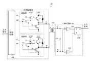
図1に示す信号伝達回路1は、1次側回路2と、2次側回路192と、トランス193とを備えて構成されている。
上記1次側回路2は、電源部3、4と、駆動回路5とを備えて構成されている。The signal transmission circuit 1 shown in FIG. 1 includes a
The
上記電源部3、4は、それぞれ、電圧VDDの電源とグランドとの間に設けられるnチャネルのMOSFET6、7(複数のスイッチング素子)と、電源とMOSFET6との間に設けられる抵抗8(電圧印加手段)とを備えて構成されている。 The
MOSFET6のドレイン端子は抵抗8を介して電圧VDDの電源に接続され、MOSFET6のソース端子はMOSFET7のドレイン端子に接続されている。MOSFET7のソース端子はグランドに接続されている。電源部3においてMOSFET6、7の接続点はトランス193の1次側コイルの一方端に接続され、電源部4においてMOSFET6、7の接続点はトランス193の1次側コイルの他方端に接続されている。 The drain terminal of the
なお、トランス193の1次側コイルの一方端(電源部3に接続される点)をA点とし、トランス193の1次側コイルの他方端(電源部4に接続される点)をB点とする。
図2は、図1に示す信号伝達回路1内の各回路の出力タイミングチャートを示す図である。なお、A点からB点に流れる電流値をL、電源部3の抵抗8の抵抗値をR1、電源部4の抵抗8の抵抗値をR2とし、R1とR2は互いに同じ値とする。Note that one end of the primary side coil of the transformer 193 (point connected to the power supply unit 3) is point A, and the other end of the primary side coil of the transformer 193 (point connected to the power source unit 4) is point B. And
FIG. 2 is a diagram showing an output timing chart of each circuit in the signal transmission circuit 1 shown in FIG. Note that the current value flowing from point A to point B is L, the resistance value of the
図1及び図2に示すように、入力信号の立上りタイミングにおいて、駆動回路5から電源部4のMOSFET6のゲート端子に入力される駆動信号S3がハイレベルからローレベルになり、駆動回路5から電源部4のMOSFET7のゲート端子に入力される駆動信号S4がローレベルからハイレベルになる。(このとき、駆動回路5から電源部3のMOSFET6のゲート端子に出力される駆動信号S1はハイレベルであり、駆動回路5から電源部3のMOSFET7のゲート端子に入力される駆動信号S2はローレベルである。)
すると、電源部3のMOSFET6と電源部4のMOSFET7がON、電源部3のMOSFET7と電源部4のMOSFET6がOFFとなり、1次側回路2のA点の電圧が、電源部3の抵抗8により電源電圧VDDから電圧(L×R1)降下した分の電圧(VDD−L×R1)となり、1次側回路2のB点がグランドに繋がる。したがって、1次側回路2のA点−B点間にプラス極性の電圧(VDD−L×R1)が発生し、トランス193を介して2次側回路192のC点−D点間にA点−B点間に発生したプラス極性の電圧に対応するプラス極性の電圧(VDD−L×R1)が発生する。このプラス極性の電圧(VDD−L×R1)は、コンパレータ202で設定される閾値(第1の閾値)以上の電圧であり、コンパレータ202に入力されるとコンパレータ202からハイレベルの電圧が出力される。As shown in FIGS. 1 and 2, at the rising timing of the input signal, the drive signal S3 input from the
Then, the
そして、C点−D点間にプラス極性の電圧が発生すると、コンパレータ202からフリップフロップ回路204のセット端子(S)にハイレベルの電圧が出力され、フリップフロップ回路204の出力端子(Q)から出力される電圧(出力信号)が立ち上がる。 When a positive polarity voltage is generated between the point C and the point D, a high level voltage is output from the
一方、入力信号の立下りタイミングにおいて、駆動信号S1がハイレベルからローレベルになり、駆動信号S2がローレベルからハイレベルになる。(このとき、駆動信号S3はハイレベルであり、駆動信号S4はローレベルである。)
すると、電源部3のMOSFET7と電源部4のMOSFET6がON、電源部3のMOSFET6と電源部4のMOSFET7がOFFとなり、1次側回路2のA点がグランドに接続され、1次側回路2のB点が、電源部4の抵抗8により電源電圧VDDから電圧(L×R2)降下した分の電圧(VDD−L×R2)となる。したがって、1次側回路2のA点−B点間にマイナス極性の電圧(−(VDD−L×R2))が発生し、トランス193を介して2次側回路192のC点−D点間にA点−B点間に発生したマイナス極性の電圧に対応するマイナス極性の電圧(−(VDD−L×R2))が発生する。このマイナス極性の電圧(−(VDD−L×R2))は、コンパレータ203で設定される閾値(第2の閾値)以上の電圧であり、コンパレータ203に入力されるとコンパレータ203からハイレベルの電圧が出力される。On the other hand, at the falling timing of the input signal, the drive signal S1 changes from high level to low level, and the drive signal S2 changes from low level to high level. (At this time, the drive signal S3 is at a high level and the drive signal S4 is at a low level.)
Then, the
そして、C点−D点間にマイナス極性の電圧が発生すると、コンパレータ203からフリップフロップ回路204のリセット端子(R)にハイレベルの電圧が出力され、フリップフロップ回路204の出力端子(Q)から出力される電圧が立ち下がる。 When a negative polarity voltage is generated between the point C and the point D, a high level voltage is output from the
このように、図1に示す信号伝達回路1は、入力信号と同じ立上りタイミング及び立下りタイミングの出力信号をトランス193を介して出力することができる。
入力信号の立上りタイミング後、本実施形態の信号伝達回路1では、駆動信号S3がローレベルからハイレベルに戻り、駆動信号S4がハイレベルからローレベルに戻る。(このとき、駆動信号S1はハイレベル、駆動信号S2はローレベルである。)
すると、トランス193の1次側コイルの一端(A点)が電源部3のMOSFET6、電源部3の抵抗8を介して電源部3の電源(VDD)に接続され、1次コイルの他端(B点)が電源部4のMOSFET6、電源部4の抵抗8を介して電源部4の電源(VDD)に接続されるため、A点−B点間にマイナス極性の電圧(−(L×(R2+R1)))が発生するとともに、電源部3の電源(VDD)、電源部3の抵抗8、電源部3のMOSFET6、トランス193の1次側コイル、電源部4のMOSFET7、電源部4のグランドの順に流れていた電流が、電源部3の電源(VDD)、電源部3の抵抗8、電源部3のMOSFET6、トランス193の1次側コイル、電源部4のMOSFET6、電源部4の抵抗8、電源部4の電源(VDD)の順に流れる。したがって、トランス193に蓄積されたエネルギーが電源部4の抵抗8によって消費され、トランス193に蓄積されたエネルギーがリセットされる。そして、トランス193に蓄積されたエネルギーがリセットされると、トランス193の1次側コイルに流れる電流はゼロになり、A点、B点の電圧はVDDとなる。As described above, the signal transmission circuit 1 shown in FIG. 1 can output the output signal having the same rise timing and fall timing as the input signal via the
After the rising timing of the input signal, in the signal transmission circuit 1 of the present embodiment, the drive signal S3 returns from the low level to the high level, and the drive signal S4 returns from the high level to the low level. (At this time, the drive signal S1 is at a high level and the drive signal S2 is at a low level.)
Then, one end (point A) of the primary side coil of the
なお、このときA点−B点間に発生するマイナス極性の電圧(−(L×(R2+R1)))はコンパレータ203からハイレベルの電圧が出力されない大きさの電圧とする。すなわち、マイナス極性の電圧(−(L×(R2+R1)))は上記第2の閾値未満の電圧とする。 Note that a negative polarity voltage (− (L × (R2 + R1))) generated between the points A and B at this time is a voltage that does not output a high level voltage from the
また、入力信号の立下りタイミング後、駆動信号S1がローレベルからハイレベルに戻り、駆動信号S2がハイレベルからローレベルに戻る。(このとき、駆動信号S3はハイレベル、駆動信号S4はローレベルである)
すると、トランス193の1次側コイルの一方端(A点)が電源部3のMOSFET6、電源部3の抵抗8を介して電源部3の電源(VDD)に接続され、1次コイルの他方端(B点)が電源部4のMOSFET6、電源部4の抵抗8を介して電源部3の電源(VDD)に接続されるため、A点−B点間にプラス極性の電圧(L×(R1+R2))が発生するとともに、電源部4の電源(VDD)、電源部4の抵抗8、電源部4のMOSFET6、トランス193の1次側コイル、トランス193の1次側コイル、電源部3のMOSFET7、電源部3のグランドの順に流れていた電流が、電源部4の電源(VDD)、電源部4の抵抗8、電源部4のMOSFET6、トランス193の1次側コイル、電源部3のMOSFET6、電源部3の抵抗8、電源部3の電源(VDD)の順に流れる。したがって、トランス193の1次側コイルに蓄積されたエネルギーが電源部3の抵抗8によって消費され、トランス193に蓄積されたエネルギーがリセットされる。そして、トランス193に蓄積されたエネルギーがリセットされると、トランス193に流れる電流はゼロになり、A点、B点の電圧はVDDとなる。In addition, after the falling timing of the input signal, the drive signal S1 returns from the low level to the high level, and the drive signal S2 returns from the high level to the low level. (At this time, the drive signal S3 is at a high level and the drive signal S4 is at a low level)
Then, one end (point A) of the primary side coil of the
なお、このときA点−B点間に発生するプラス極性の電圧(L×(R1+R2))はコンパレータ202からハイレベルの電圧が出力されない大きさの電圧とする。すなわち、プラス極性の電圧(L×(R1+R2))は上記第1の閾値未満の電圧とする。 At this time, the positive polarity voltage (L × (R1 + R2)) generated between the points A and B is set to a voltage that does not output a high-level voltage from the
以上のように、図1に示す信号伝達回路1は、トランス193の結合係数が悪くても、入力信号の立上りタイミング後や立下りタイミング後においてトランス193に蓄積されるエネルギーをリセットさせることができるので、トランス193の2次側回路192における発振を防止することができ、誤動作を抑えることができる。 As described above, the signal transmission circuit 1 shown in FIG. 1 can reset the energy accumulated in the
図3は、本発明の第2の実施形態の信号伝達回路を示す図である。なお、図1に示す信号伝達回路1の構成と同じ構成には同じ符号を付し、その構成の説明を省略する。
図3に示す信号伝達回路9は、1次側回路10と、2次側回路192と、トランス193とを備えて構成されている。FIG. 3 is a diagram showing a signal transmission circuit according to the second embodiment of the present invention. In addition, the same code | symbol is attached | subjected to the same structure as the structure of the signal transmission circuit 1 shown in FIG. 1, and description of the structure is abbreviate | omitted.
The signal transmission circuit 9 shown in FIG. 3 includes a primary circuit 10, a secondary circuit 192, and a
上記1次側回路10は、電源部11、12と、駆動回路5とを備えて構成されている。
上記電源部11、12は、それぞれ、MOSFET6、7と、抵抗8と、抵抗8に並列接続されるダイオード13(電圧印加手段)とを備えて構成されている。The primary side circuit 10 includes
Each of the
図4は、図3に示す信号伝達回路9の各回路の出力タイミングチャートを示す図である。なお、ダイオード13の閾値電圧をVF1とする。
図3及び図4に示すように、入力信号の立上りタイミングにおいて、駆動信号S3がハイレベルからローレベルになり、駆動信号S4がローレベルからハイレベルになる。(このとき、駆動信号S1はハイレベルであり、駆動信号S2はローレベルである。)
すると、電源部11のMOSFET6と電源部12のMOSFET7がON、電源部11のMOSFET7と電源部12のMOSFET6がOFFとなり、1次側回路2のA点が、電源電圧VDDから電圧VF1降下した分の電圧(VDD−VF1)となり、1次側回路2のB点がグランドに繋がる。したがって、1次側回路2のA点−B点間にプラス極性の電圧(VDD−VF1)が発生し、トランス193を介して2次側回路192のC点−D点間にA点−B点間に発生したプラス極性の電圧に対応するプラス極性の電圧(VDD−VF1)が発生する。FIG. 4 is a diagram showing an output timing chart of each circuit of the signal transmission circuit 9 shown in FIG. Note that the threshold voltage of the
As shown in FIGS. 3 and 4, at the rising timing of the input signal, the drive signal S3 changes from high level to low level, and the drive signal S4 changes from low level to high level. (At this time, the drive signal S1 is at a high level and the drive signal S2 is at a low level.)
Then, the
そして、C点−D点間にプラス極性の電圧が発生すると、コンパレータ202からフリップフロップ回路204のセット端子(S)にハイレベルの電圧が出力され、フリップフロップ回路204の出力端子(Q)から出力される電圧(出力信号)が立ち上がる。 When a positive polarity voltage is generated between the point C and the point D, a high level voltage is output from the
一方、入力信号の立下りタイミングにおいて、駆動信号S1がハイレベルからローレベルになり、駆動信号S2がローレベルからハイレベルになる。(このとき、駆動信号S3はハイレベルであり、駆動信号S4はローレベルである。)
すると、電源部11のMOSFET7と電源部12のMOSFET6がON、電源部11のMOSFET6と電源部12のMOSFET7がOFFとなり、1次側回路2のA点がグランドに繋がり、1次側回路2のB点が電源電圧VDDから電圧VF1降下した分の電圧(VDD−VF1)となる。したがって、1次側回路2のA点−B点間にマイナス極性の電圧(−(VDD−VF1))が発生し、トランス193を介してC点−D点間にA点−B点間に発生したマイナス極性の電圧に対応するマイナス極性の電圧(−(VDD−VF1))が発生する。On the other hand, at the falling timing of the input signal, the drive signal S1 changes from high level to low level, and the drive signal S2 changes from low level to high level. (At this time, the drive signal S3 is at a high level and the drive signal S4 is at a low level.)
Then, the
そして、C点−D点間にマイナス極性の電圧が発生すると、コンパレータ203からフリップフロップ回路204のリセット端子(R)にハイレベルの電圧が出力され、フリップフロップ回路204の出力端子(Q)から出力される電圧が立ち下がる。 When a negative polarity voltage is generated between the point C and the point D, a high level voltage is output from the
このように、図3に示す信号伝達回路9は、入力信号と同じ立上りタイミング及び立下りタイミングの出力信号をトランス193を介して出力することができる。
入力信号の立上りタイミング後、駆動信号S3がローレベルからハイレベルに戻り、駆動信号S4がハイレベルからローレベルに戻る。(このとき、駆動信号S1はハイレベル、駆動信号S2はローレベルである。)
すると、トランス193の1次側コイルの一端(A点)が電源部11のMOSFET6、電源部11のダイオード13を介して電源部11の電源(VDD)に接続され、1次コイルの他端(B点)が電源部12のMOSFET6、電源部12の抵抗8を介して電源部12の電源(VDD)に接続されるため、A点−B点間には、マイナス極性の電圧(L×R2+VF1)が発生するとともに、電源部11の電源(VDD)、電源部11のダイオード13、電源部11のMOSFET6、トランス193の1次側コイル、電源部12のMOSFET7、電源部12のグランドの順に流れていた電流が、電源部11の電源(VDD)、電源部11のダイオード13、電源部11のMOSFET6、トランス193の1次側コイル、電源部12のMOSFET6、電源部12の抵抗8、電源部12の電源(VDD)の順に流れる。したがって、トランス193に蓄積されたエネルギーが電源部12の電源(VDD)の抵抗8によって消費され、トランス193に蓄積されたエネルギーがリセットされる。そして、トランス193に蓄積されたエネルギーがリセットされると、トランス193の1次側コイルに流れる電流はゼロになり、A点、B点の電圧はVDDとなる。As described above, the signal transmission circuit 9 shown in FIG. 3 can output the output signal having the same rise timing and fall timing as the input signal via the
After the rising timing of the input signal, the drive signal S3 returns from the low level to the high level, and the drive signal S4 returns from the high level to the low level. (At this time, the drive signal S1 is at a high level and the drive signal S2 is at a low level.)
Then, one end (point A) of the primary side coil of the
なお、このときA点−B点間に発生するマイナス極性の電圧(−(L×R2+VF1))はコンパレータ203からハイレベルの電圧が出力されない大きさの電圧とする。すなわち、マイナス極性の電圧(−(L×R2+VF1))は上記第2の閾値未満の電圧とする。 Note that the negative polarity voltage (− (L × R2 + VF1)) generated between the points A and B at this time is a voltage that does not output a high level voltage from the
また、入力信号の立下りタイミング後、駆動信号S1がローレベルからハイレベルに戻り、駆動信号S2がハイレベルからローレベルに戻る。(このとき、駆動信号S3はハイレベル、駆動信号S4はローレベルである)
すると、トランス193の1次側コイルの一端(A点)が電源部11のMOSFET6、電源部11の抵抗8を介して電源部11の電源(VDD)に接続され、1次コイルの他端(B点)が電源部12のMOSFET6、電源部12のダイオード13を介して電源部12の電源(VDD)に接続されるため、A点−B点間には、正のプラス極性の電圧として(L×R1+VF1)が発生するとともに、電源部12の電源(VDD)、電源部12のダイオード13、電源部12のMOSFET6、トランス193の1次側コイル、電源部11のMOSFET7、電源部11のグランドの順に流れていた電流が、電源部12の電源(VDD)、電源部12のダイオード13、電源部12のMOSFET6、トランス193の1次側コイル、電源部11のMOSFET6、電源部11の抵抗8、電源部11の電源(VDD)の順に流れる。したがって、トランス193の1次側コイルに蓄積されたエネルギーが電源部11の抵抗8によって消費され、このとき、トランス193に蓄積されたエネルギーがリセットされる。そして、トランス193に蓄積されたエネルギーがリセットされると、トランス193に流れる電流はゼロになり、A点、B点の電圧は電源電圧VDDになる。In addition, after the falling timing of the input signal, the drive signal S1 returns from the low level to the high level, and the drive signal S2 returns from the high level to the low level. (At this time, the drive signal S3 is at a high level and the drive signal S4 is at a low level)
Then, one end (point A) of the primary side coil of the
なお、このときA点−B点間に発生するプラス極性の電圧(L×R1+VF1)はコンパレータ202からハイレベルの電圧が出力されない大きさの電圧とする。すなわち、プラス極性の電圧(L×R1+VF1)は上記第1の閾値未満の電圧とする。 At this time, the positive polarity voltage (L × R1 + VF1) generated between the points A and B is set to a voltage that does not output a high level voltage from the
従って、図3に示す信号伝達回路9は、トランス193の結合係数が悪くても、入力信号の立上りタイミング後や立下りタイミング後において、トランス193の2次側回路における発振を防止することができるので、誤動作することがない。 Therefore, even if the coupling coefficient of the
図5は、本発明の第3の実施形態の信号伝達回路を示す図である。なお、図1に示す信号伝達回路1や図20に示す信号伝達回路190と同じ構成には同じ符号を付し、その説明を省略する。 FIG. 5 is a diagram showing a signal transmission circuit according to the third embodiment of the present invention. In addition, the same code | symbol is attached | subjected to the same structure as the signal transmission circuit 1 shown in FIG. 1, and the
図5に示す信号伝達回路14は、1次側回路15と、2次側回路192と、トランス193とを備えて構成されている。
上記1次側回路15は、電源部16、17と、駆動回路196とを備えて構成されている。The signal transmission circuit 14 shown in FIG. 5 includes a
The
上記電源部16、17は、それぞれ、npnバイポーラトランジスタ18(電圧印加手段)と、nチャネルのMOSFET19、20(複数のスイッチング素子)と、ダイオード21(電圧印加手段)と、抵抗22(電圧印加手段)と、定電流源23とを備えて構成されている。 The
npnバイポーラトランジスタ18のコレクタ端子は電圧VDDの電源及びダイオード21のカソード端子に接続されていると共に定電流源23を介してMOSFET20のドレイン端子及びnpnバイポーラトランジスタ18のベース端子に接続され、npnバイポーラトランジスタ18のエミッタ端子はMOSFET19のドレイン端子に接続されていると共に抵抗22を介してダイオード21のアノード端子に接続されている。MOSFET19、20のそれぞれのゲート端子は互いに接続され、MOSFET19、20のそれぞれのソース端子はグランドに接続されている。電源部16においてnpnバイポーラトランジスタ18とMOSFET19との接続点はトランス193の1次側コイルの一方端に接続され、電源部17においてnpnバイポーラトランジスタ18とMOSFET19との接続点はトランス193の1次側コイルの他方端に接続されている。 The collector terminal of the npn
図6は、図5に示す信号伝達回路14の各回路の出力タイミングチャートを示す図である。なお、電源部16の抵抗22の抵抗値をR3、電源部17の抵抗22の抵抗値をR4、npnバイポーラトランジスタ18のベース−エミッタ間電圧をVbe、ダイオード21の閾値電圧をVF2とする。 FIG. 6 is a diagram showing an output timing chart of each circuit of the signal transmission circuit 14 shown in FIG. The resistance value of the
図5及び図6に示すように、入力信号の立上りタイミングにおいて、駆動信号M1がローレベルからハイレベルになる。(このとき、駆動信号M2はローレベルである。)
すると、電源部16のnpnバイポーラトランジスタ18と電源部17のMOSFET19とがON、電源部16のMOSFET19と電源部17のnpnバイポーラトランジスタ18がOFFとなり、1次側回路15のB点がグランド電圧に繋がり、1次側回路15のA点が電源電圧VDDから電圧Vbe降下した分の電圧(VDD−Vbe)となる。したがって、1次側回路15のA点−B点間にプラス極性の電圧(VDD−Vbe)が発生し、トランス193を介して2次側回路192のC点−D点間電圧にA点−B点間に発生したプラス極性の電圧に対応するプラス極性の電圧(VDD−Vbe)が発生する。As shown in FIGS. 5 and 6, the drive signal M1 changes from the low level to the high level at the rising timing of the input signal. (At this time, the drive signal M2 is at a low level.)
Then, the npn
そして、C点−D点間にプラス極性の電圧が発生すると、コンパレータ202からフリップフロップ回路204のセット端子(S)にハイレベルの電圧が出力され、フリップフロップ回路204の出力端子(Q)から出力される電圧(出力信号)が立ち上がる。 When a positive polarity voltage is generated between the point C and the point D, a high level voltage is output from the
一方、入力信号の立下りタイミングにおいて、駆動信号M2がローレベルからハイレベルになる。(このとき、駆動信号M1はローレベルである。)
すると、電源部16のMOSFET19と電源部17のnpnバイポーラトランジスタ18とがON、電源部16のnpnバイポーラトランジスタ18と電源部17のMOSFET19がOFFとなり、1次側回路15のA点がグランドに繋がり、1次側回路15のB点が電源電圧VDDから電圧Vbe降下した分の電圧(VDD−Vbe)となる。したがって、1次側回路15のA点−B点間にマイナス極性の電圧(−(VDD−Vbe))が発生し、トランス193を介してC点−D点間電圧にA点−B点間に発生したマイナス極性の電圧に対応するマイナス極性の電圧(−(VDD−Vbe))が発生する。On the other hand, the drive signal M2 changes from the low level to the high level at the falling timing of the input signal. (At this time, the drive signal M1 is at a low level.)
Then, the
そして、C点−D点間にマイナス極性の電圧が発生すると、コンパレータ203からフリップフロップ回路204のリセット端子(R)にハイレベルの電圧が出力され、フリップフロップ回路204の出力端子(Q)から出力される電圧が立ち下がる。 When a negative polarity voltage is generated between the point C and the point D, a high level voltage is output from the
このように、図5に示す信号伝達回路14は、入力信号と同じ立上りタイミング及び立下りタイミングの出力信号をトランス193を介して出力することができる。
入力信号の立上りタイミング後、駆動信号M1がハイレベルからローレベルに戻る。As described above, the signal transmission circuit 14 illustrated in FIG. 5 can output the output signal having the same rising timing and falling timing as the input signal via the
After the rising timing of the input signal, the drive signal M1 returns from the high level to the low level.
すると、トランス193の1次側コイルの一端(A点)が電源部16のnpnバイポーラトランジスタ18を介して電源部16の電源(VDD)に接続され、1次コイルの他端(B点)が電源部17の抵抗22、電源部17のダイオード21を介して電源部17の電源(VDD)に接続されるため、A点−B点間に負のマイナス極性の電圧として(L×R4+VF2+Vbe)が発生するとともに、電源部16の電源(VDD)、電源部16のnpnバイポーラトランジスタ18、トランス193の1次側コイル、電源部17のMOSFET19、電源部17のグランドの順に流れていた電流が、電源部16の電源(VDD)、電源部16のnpnバイポーラトランジスタ18、トランス193の1次側コイル、電源部17の抵抗22、電源部17のダイオード21、電源部17の電源(VDD)の順に流れる。したがって、トランス193に蓄積されたエネルギーが電源部17のダイオード21および抵抗22によって消費され、トランス193に蓄積されたエネルギーがリセットされる。そして、トランス193に蓄積されたエネルギーがリセットされると、トランス193に流れる電流はゼロになり、A点、B点の電圧は電源電圧VDDになる。 Then, one end (point A) of the primary coil of the
なお、このときA点−B点間に発生するマイナス極性の電圧(L×R4+VF2+Vbe)はコンパレータ203からハイレベルの電圧が出力されない大きさの電圧とする。すなわち、マイナス極性の電圧(L×R4+VF2+Vbe)は上記第2の閾値未満の電圧とする。 Note that the negative polarity voltage (L × R4 + VF2 + Vbe) generated between the points A and B at this time is a voltage that does not output a high-level voltage from the
また、入力信号の立下りタイミング後、駆動信号M2がハイレベルからローレベルに戻る。
すると、トランス193の1次側コイルの一端(A点)が1次コイルの他端が電源部16の抵抗22、電源部16のダイオード21を介して電源部16の電源(VDD)に接続され、1次コイルの他端(B点)が電源部17のnpnバイポーラトランジスタ18を介して電源部17の電源(VDD)に接続されるため、A点−B点間にプラス極性の電圧(L×R3+VF2+Vbe)が発生するとともに、電源部17の電源(VDD)、電源部17のnpnバイポーラトランジスタ18、トランス193の1次側コイル、電源部16のMOSFET19、電源部16のグランドの順に流れていた電流が、電源部17の電源(VDD)、電源部17のnpnバイポーラトランジスタ18、トランス193の1次側コイル、電源部16の抵抗22、電源部16のダイオード21、電源部16の電源(VDD)の順に流れる。したがって、トランス193の1次側コイルに蓄積されたエネルギーが電源部16のダイオード21および抵抗22によって消費され、トランス193に蓄積されたエネルギーがリセットされる。そして、トランス193に蓄積されたエネルギーがリセットされると、トランス193に流れる電流はゼロになり、A点、B点の電圧は電源電圧VDDになる。In addition, after the falling timing of the input signal, the drive signal M2 returns from the high level to the low level.
Then, one end (point A) of the primary side coil of the
なお、このときA点−B点間に発生するプラス極性の電圧(L×R3+VF2+Vbe)はコンパレータ202からハイレベルの電圧が出力されない大きさの電圧とする。すなわち、プラス極性の電圧(L×R3+VF2+Vbe)は上記第1の閾値未満の電圧とする。 At this time, the positive polarity voltage (L × R3 + VF2 + Vbe) generated between the points A and B is a voltage that does not output a high level voltage from the
従って、図5に示す信号伝達回路14は、トランス193の結合係数が悪くても、入力信号の立上りタイミング後や立下りタイミング後において、2次側回路における発振を防止することができるので、誤動作することがない。 Therefore, even if the coupling coefficient of the
図7は、本発明の第4の実施形態の信号伝達回路を示す図である。なお、図1に示す信号伝達回路1や図5に示す信号伝達回路14と同じ構成には同じ符号を付し、その説明を省略する。 FIG. 7 is a diagram showing a signal transmission circuit according to the fourth embodiment of the present invention. The same components as those of the signal transmission circuit 1 shown in FIG. 1 and the signal transmission circuit 14 shown in FIG.
図7に示す信号伝達回路24は、1次側回路25と、2次側回路192と、トランス193とを備えて構成されている。
上記1次側回路25は、電源部26、27と、駆動回路196とを備えて構成されている。The
The
上記電源部26、27は、それぞれ、npnバイポーラトランジスタ18と、MOSFET19、20と、ダイオード21(電圧印加手段)と、定電流源23とを備えて構成されている。 Each of the
npnバイポーラトランジスタ18のコレクタ端子は電圧VDDの電源及びダイオード21のカソード端子に接続されていると共に定電流源23を介してMOSFET20のドレイン端子及びnpnバイポーラトランジスタ18のベース端子に接続され、npnバイポーラトランジスタ18のエミッタ端子はMOSFET19のドレイン端子及びダイオード21のアノード端子に接続されている。MOSFET19、20のそれぞれのゲート端子は互いに接続され、MOSFET19、20のそれぞれのソース端子はグランドに接続されている。電源部26においてnpnバイポーラトランジスタ18とMOSFET19との接続点はトランス193の1次側コイルの一方端に接続され、電源部27においてnpnバイポーラトランジスタ18とMOSFET19との接続点はトランス193の1次側コイルの他方端に接続されている。 The collector terminal of the npn
図8は、図7に示す信号伝達回路24の各回路の出力タイミングチャートを示す図である。なお、npnバイポーラトランジスタ18のベース−エミッタ間電圧をVbe、ダイオード21の閾値にかかる電圧をVF2とする。 FIG. 8 is a diagram showing an output timing chart of each circuit of the
図7及び図8に示すように、入力信号の立上りタイミングにおいて、駆動信号M1がローレベルからハイレベルになる。(このとき、駆動信号M2はローレベルである。)
すると、電源部26のnpnバイポーラトランジスタ18と電源部27のMOSFET19とがON、電源部26のMOSFET19と電源部27のnpnバイポーラトランジスタ18とがOFFとなり、1次側回路25のB点がグランドに繋がり、1次側回路25のA点が電源電圧VDDから電圧Vbe降下した分の電圧(VDD−Vbe)となる。したがって、1次側回路25のA点−B点間にプラス極性の電圧(VDD−Vbe)が発生し、トランス193を介して2次側回路192のC点−D点間電圧にA点−B点間に発生したプラス極性の電圧に対応するプラス極性の電圧(VDD−Vbe)が発生する。As shown in FIGS. 7 and 8, the drive signal M1 changes from the low level to the high level at the rising timing of the input signal. (At this time, the drive signal M2 is at a low level.)
Then, the npn
そして、C点−D点間にプラス極性の電圧が発生すると、コンパレータ202からフリップフロップ回路204のセット端子(S)にハイレベルの電圧が出力され、フリップフロップ回路204の出力端子(Q)から出力される電圧(出力信号)が立ち上がる。 When a positive polarity voltage is generated between the point C and the point D, a high level voltage is output from the
一方、入力信号の立下りタイミングにおいて、駆動信号M2がローレベルからハイレベルになる。(このとき、駆動信号M1はローレベルである。)
すると、電源部26のMOSFET19と電源部27のnpnバイポーラトランジスタ18とがON、電源部26のnpnバイポーラトランジスタ18と電源部27のMOSFET19とがOFFとなり、1次側回路25のA点がグランドと繋がり、1次側回路25のB点が電源電圧VDDから電圧Vbe降下した分の電圧(VDD−Vbe)となる。したがって、1次側回路25のA点−B点間にマイナス極性の電圧(−(VDD−Vbe))が発生し、トランス193を介しC点−D点間にマイナス極性の電圧(−(VDD−Vbe))が発生する。On the other hand, the drive signal M2 changes from the low level to the high level at the falling timing of the input signal. (At this time, the drive signal M1 is at a low level.)
Then, the
そして、C点−D点間にマイナス極性の電圧が発生すると、コンパレータ203からフリップフロップ回路204のリセット端子(R)にハイレベルの電圧が出力され、フリップフロップ回路204の出力端子(Q)から出力される電圧が立ち下がる。 When a negative polarity voltage is generated between the point C and the point D, a high level voltage is output from the
なお、コンパレータ202、203は、C点―D点間電圧が(VDD−Vbe)と(Vbe+VF2)との間の電圧のときに、ハイレベルの電圧が出力されるように設定されているものとする。但し、(VDD−Vbe)>(Vbe+VF2)とする。 The
このように、図7に示す信号伝達回路24は、入力信号と同じ立上りタイミング及び立下りタイミングの出力信号をトランス193を介して出力する。
入力信号の立上りタイミング後、本実施形態の信号伝達回路24では、駆動信号M1がハイレベルからローレベルに戻る。As described above, the
After the rising timing of the input signal, in the
すると、トランス193の1次側コイルの一端(A点)が電源部26のnpnバイポーラトランジスタ18を介して電源部26の電源(VDD)に接続され、1次コイルの他端(B点)が電源部27のダイオード21を介して電源部27の電源(VDD)に接続されるため、A点−B点間にマイナス極性の電圧(−(VF2+Vbe))発生するとともに、電源部26の電源(VDD)、電源部26のnpnバイポーラトランジスタ18、トランス193の1次側コイル、電源部27のMOSFET19、電源部27のグランドの順に流れていた電流が、電源部26の電源(VDD)、電源部26のnpnバイポーラトランジスタ18、トランス193の1次側コイル、電源部27のダイオード21、電源部27の電源(VDD)の順に流れる。したがって、トランス193の1次側コイルに蓄積されたエネルギーが電源部27のダイオード21によって消費され、1次側コイルに蓄積されたエネルギーがリセットされる。そして、トランス193に蓄積されたエネルギーがリセットされると、トランス193に流れる電流はゼロになり、A点、B点の電圧は電源電圧VDDになる。 Then, one end (point A) of the primary coil of the
なお、このときA点−B点間に発生するマイナス極性の電圧(−(VF2+Vbe))はコンパレータ203からハイレベルの電圧が出力されない大きさの電圧とする。すなわち、マイナス極性の電圧(−(VF2+Vbe))は上記第2の閾値未満の電圧とする。 Note that the negative polarity voltage (− (VF2 + Vbe)) generated between the points A and B at this time is a voltage that does not output a high level voltage from the
一方、入力信号の立下りタイミング後も、本実施形態の信号伝達回路1では、駆動信号M2がハイレベルからローレベルに戻る。
すると、トランス193の1次側コイルの一端(A点)が電源部26のダイオード21を介して電源部16の電源(VDD)に接続され、1次コイルの他端(B点)が電源部27のnpnバイポーラトランジスタ18を介して電源部17の電源(VDD)に接続されるため、A点−B点間にプラス極性の電圧(VF2+Vbe)が発生するとともに、電源部27の電源(VDD)、電源部27のnpnバイポーラトランジスタ18、トランス193の1次側コイル、電源部26のMOSFET19、電源部26のグランドの順に流れていた電流が、電源部27の電源(VDD)、電源部27のnpnバイポーラトランジスタ18、トランス193の1次側コイル、電源部26のダイオード21、電源部26の電源(VDD)の順に流れる。したがって、トランス193に蓄積されたエネルギーが電源部26のダイオード21によって消費され、トランス193の1次側コイルに蓄積されたエネルギーがリセットされる。そして、トランス193に蓄積されたエネルギーがリセットされると、トランス193に流れる電流はゼロになり、A点、B点の電圧は電源電圧VDDになる。On the other hand, even after the falling timing of the input signal, in the signal transmission circuit 1 of the present embodiment, the drive signal M2 returns from the high level to the low level.
Then, one end (A point) of the primary side coil of the
なお、このときA点−B点間に発生するプラス極性の電圧(VF2+Vbe)はコンパレータ202からハイレベルの電圧が出力されない大きさの電圧とする。すなわち、プラス極性の電圧(VF2+Vbe)は上記第1の閾値未満の電圧とする。 At this time, the positive polarity voltage (VF2 + Vbe) generated between the point A and the point B is a voltage that does not output a high level voltage from the
従って、図7に示す信号伝達回路24は、トランス193の結合係数が悪くても、入力信号の立上りタイミング後や立下りタイミング後において、2次側回路192における発振を防止することができるので、誤動作することがない。 Therefore, even if the coupling coefficient of the
図9は、本発明の第5の実施形態の信号伝達回路を示す図である。なお、図7に示す信号伝達回路24と同じ構成には同じ符号を付し、その説明を省略する。
図9に示す信号伝達回路70において、図7に示す信号伝達回路24と異なる点は、電源部26、27のそれぞれの定電流源23が電圧VDDの電源に接続されているのではなく、電圧VCCの電源に接続されている点である。なお、電圧VDDは、電圧VCCよりも低く、例えば、電圧VDDを6V、電圧VCCを5Vとする。FIG. 9 is a diagram showing a signal transmission circuit according to the fifth embodiment of the present invention. In addition, the same code | symbol is attached | subjected to the same structure as the
The
図9に示す信号伝達回路70の動作について説明する。なお、駆動回路196から出力される駆動信号M1、M2は、図8に示す駆動信号M1、M2と同じものとする。
入力信号の立上りタイミングにおいて、駆動信号M1がローレベルからハイレベルになる。(このとき、駆動信号M2はローレベルである。)
すると、電源部26のnpnバイポーラトランジスタ18と電源部27のMOSFET19とがON、電源部26のMOSFET19と電源部27のnpnバイポーラトランジスタ18とがOFFとなり、1次側回路25のB点がグランドに繋がり、1次側回路25のA点が電源電圧VCCから電圧Vbe降下した分の電圧(VCC−Vbe)となる。したがって、1次側回路25のA点−B点間にプラス極性の電圧(VCC−Vbe)が発生し、トランス193を介して2次側回路192のC点−D点間電圧にA点−B点間に発生したプラス極性の電圧に対応するプラス極性の電圧(VCC−Vbe)が発生する。The operation of the
At the rising timing of the input signal, the drive signal M1 changes from the low level to the high level. (At this time, the drive signal M2 is at a low level.)
Then, the npn
そして、C点−D点間にプラス極性の電圧が発生すると、コンパレータ202からフリップフロップ回路204のセット端子(S)にハイレベルの電圧が出力され、フリップフロップ回路204の出力端子(Q)から出力される電圧(出力信号)が立ち上がる。 When a positive polarity voltage is generated between the point C and the point D, a high level voltage is output from the
一方、入力信号の立下りタイミングにおいて、駆動信号M2がローレベルからハイレベルになる。(このとき、駆動信号M1はローレベルである。)
すると、電源部26のMOSFET19と電源部27のnpnバイポーラトランジスタ18とがON、電源部26のnpnバイポーラトランジスタ18と電源部27のMOSFET19とがOFFとなり、1次側回路25のA点がグランドと繋がり、1次側回路25のB点が電源電圧VCCから電圧Vbe降下した分の電圧(VCC−Vbe)となる。したがって、1次側回路25のA点−B点間にマイナス極性の電圧(−(VCC−Vbe))が発生し、トランス193を介しC点−D点間にマイナス極性の電圧(−(VCC−Vbe))が発生する。On the other hand, the drive signal M2 changes from the low level to the high level at the falling timing of the input signal. (At this time, the drive signal M1 is at a low level.)
Then, the
そして、C点−D点間にマイナス極性の電圧が発生すると、コンパレータ203からフリップフロップ回路204のリセット端子(R)にハイレベルの電圧が出力され、フリップフロップ回路204の出力端子(Q)から出力される電圧が立ち下がる。 When a negative polarity voltage is generated between the point C and the point D, a high level voltage is output from the
なお、(VCC−Vbe)>(VDD+VF2)とする。
このように、図9に示す信号伝達回路70は、入力信号と同じ立上りタイミング及び立下りタイミングの出力信号をトランス193を介して出力する。Note that (VCC-Vbe)> (VDD + VF2).
As described above, the
入力信号の立上りタイミング後、本実施形態の信号伝達回路70では、駆動信号M1がハイレベルからローレベルに戻る。
すると、トランス193の1次側コイルの一端(A点)が電源部26のnpnバイポーラトランジスタ18を介して電源部16の電源(VDD)に接続され、1次コイルの他端(B点)が電源部27のダイオード21を介して電源部17の電源(VDD)に接続されるため、A点−B点間にマイナス極性の電圧(−((VDD−VCC)+VF2+Vbe))発生するとともに、電源部26の電源(VDD)、電源部26のnpnバイポーラトランジスタ18、トランス193の1次側コイル、電源部27のMOSFET19、電源部27のグランドの順に流れていた電流が、電源部26の電源(VDD)、電源部26のnpnバイポーラトランジスタ18、トランス193の1次側コイル、電源部27のダイオード21、電源部27の電源(VDD)の順に流れる。したがって、トランス193の1次側コイルに蓄積されたエネルギーが電源部27のダイオード21によって消費され、1次側コイルに蓄積されたエネルギーがリセットされる。After the rising timing of the input signal, in the
Then, one end (point A) of the primary coil of the
なお、このときA点−B点間に発生するマイナス極性の電圧(−((VDD−VCC)+VF2+Vbe))はコンパレータ203からハイレベルの電圧が出力されない大きさの電圧とする。すなわち、マイナス極性の電圧(−((VDD−VCC)+VF2+Vbe))は上記第2の閾値未満の電圧とする。 Note that a negative polarity voltage (− ((VDD−VCC) + VF2 + Vbe)) generated between the points A and B at this time is a voltage that does not output a high level voltage from the
一方、入力信号の立下りタイミング後も、本実施形態の信号伝達回路70では、駆動信号M2がハイレベルからローレベルに戻る。
すると、トランス193の1次側コイルの一端(A点)が電源部26のダイオード21を介して電源部26の電源(VDD)に接続され、1次コイルの他端(B点)が電源部27のnpnバイポーラトランジスタ18を介して電源部17の電源(VDD)に接続されるため、A点−B点間にプラス極性の電圧((VDD−VCC)+VF2+Vbe)が発生するとともに、電源部27の電源(VDD)、電源部27のnpnバイポーラトランジスタ18、トランス193の1次側コイル、電源部26のMOSFET19、電源部26のグランドの順に流れていた電流が、電源部27の電源(VDD)、電源部27のnpnバイポーラトランジスタ18、トランス193の1次側コイル、電源部26のダイオード21、電源部26の電源(VDD)の順に流れる。したがって、トランス193に蓄積されたエネルギーが電源部26のダイオード21によって消費され、トランス193の1次側コイルに蓄積されたエネルギーがリセットされる。On the other hand, even after the falling timing of the input signal, in the
Then, one end (A point) of the primary side coil of the
なお、このときA点−B点間に発生するプラス極性の電圧((VDD−VCC)+VF2+Vbe)はコンパレータ202からハイレベルの電圧が出力されない大きさの電圧とする。すなわち、プラス極性の電圧((VDD−VCC)+VF2+Vbe)は上記第1の閾値未満の電圧とする。 Note that the positive polarity voltage ((VDD−VCC) + VF2 + Vbe) generated between the points A and B at this time is a voltage that does not output a high level voltage from the
従って、図9に示す信号伝達回路70は、トランス193の結合係数が悪くても、入力信号の立上りタイミング後や立下りタイミング後において、2次側回路192における発振を防止することができるので、誤動作することがない。 Therefore, even if the coupling coefficient of the
以上のように、第1〜第5の実施の形態の信号伝達回路1、9、14、24、70は、それぞれ、トランス193の結合係数が悪いことによってトランス193の2次側回路192における発振を防止することができるので、抵抗201の抵抗値を小さくしてトランス193の2次側回路192における発振を抑える必要がなく、信号伝達回路1、9、14、24に流れる電流が増大してしまうことを防止することができる。 As described above, the
また、上記信号伝達回路1、9、14、24、70は、それぞれ、トランス193によりデジタル信号を1次側回路から2次側回路に伝達させる構成であるので、高信頼性、高耐久性、高速性などの優れた特性を備えた信号伝達回路になっている。 The
図10は、本発明の第6の実施形態の信号伝達回路を示す図である。なお、図7に示す構成と同じ構成には同じ符号を付し、その説明を省略する。
図10に示す実施例では、1次側回路25において、異常信号出力回路28が追加されている。また、電源部26、27において、それぞれ、コンパレータ29、定電圧源30、及び抵抗31が追加されている。また、2次側回路192において、抵抗32、33、ダイオード34〜37、及びnチャネルのMOSFET38が追加されている。なお、特許請求の範囲に記載される電流増加回路は、例えば、抵抗32及びMOSFET38により構成されるものとする。また、抵抗33の抵抗値は、抵抗32の抵抗値よりも大きいものとする。FIG. 10 is a diagram showing a signal transmission circuit according to the sixth embodiment of the present invention. In addition, the same code | symbol is attached | subjected to the same structure as the structure shown in FIG. 7, and the description is abbreviate | omitted.
In the embodiment shown in FIG. 10, an abnormal
npnバイポーラトランジスタ18のコレクタ端子は電圧VDDの電源及びダイオード21のカソード端子に接続されていると共に定電流源23を介してMOSFET20のドレイン端子及びnpnバイポーラトランジスタ18のベース端子に接続され、npnバイポーラトランジスタ18のエミッタ端子はMOSFET19のドレイン端子及びダイオード21のアノード端子に接続されている。MOSFET19、20のそれぞれのゲート端子は互いに接続され、MOSFET19のソース端子はコンパレータ29のプラスの入力端子に接続されていると共に抵抗31を介してグランドに接続されている。MOSFET20のソース端子及び定電圧源30のマイナス端子はそれぞれグランドに接続されている。コンパレータ29のマイナスの入力端子は定電圧源30のプラス端子に接続されている。電源部26においてnpnバイポーラトランジスタ18とMOSFET19との接続点はトランス193の1次側コイルの一方端に接続され、電源部27においてnpnバイポーラトランジスタ18とMOSFET19との接続点はトランス193の1次側コイルの他方端に接続されている。 The collector terminal of the npn
なお、電源部26においてMOSFET19のソース端子と抵抗31との接続点をE点とし、電源部27においてMOSFET19のソース端子と抵抗31との接続点をF点とする。 In the
また、図10に示す信号伝達回路24は、例えば、nチャネルのMOSFET90のゲート端子に出力信号を出力するものとし、MOSFET90のソース端子とグランドとの間に設けられる抵抗91にかかる電圧がプラスの入力端子に入力され、マイナスの入力端子に基準電圧V1が入力されるコンパレータ92から出力される電圧がMOSFET38のゲート端子に入力されるものとする。 The
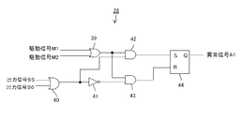
図11は、異常信号出力回路28を示す図である。
図11に示す異常信号出力回路28は、OR回路39、40と、インバータ41と、AND回路42、43と、フリップフロップ回路44とを備えて構成されている。FIG. 11 is a diagram illustrating the abnormal
The abnormal
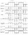
図12は、異常信号出力回路28内の各回路の出力タイミングチャートを示す図である。
例えば、何らかの原因によりMOSFET90が破壊され抵抗91に大きな電圧がかかり、コンパレータ92から出力される電圧がハイレベルになると、MOSFET38がオンする。すると、抵抗32が有効になり、2次側回路192に流れる電流が大きくなるので、トランス193の1次側コイルに流れる電流も大きくなる。このとき、入力信号が立ち上がると、または、入力信号が立ち下がると、1次側回路25のE点またはF点の電圧が正常時(コンパレータ92からローレベルの電圧が出力されているとき)よりも大きくなり、電源部26または電源部27のコンパレータ29からハイレベルのパルス電圧(出力信号S5、S6)が出力され、AND回路42からハイレベルのパルス電圧が出力される。そのため、フリップフロップ回路44から出力される電圧(異常信号A1)がローレベルからハイレベルになる。FIG. 12 is a diagram illustrating an output timing chart of each circuit in the abnormal
For example, when the MOSFET 90 is destroyed for some reason and a large voltage is applied to the resistor 91 and the voltage output from the
そして、その後、抵抗91に大きな電圧がかからなくなるなどして、コンパレータ92から出力される電圧がローレベルになると、MOSFET38がオフし、抵抗32が無効になるので、2次側回路192に流れる電流が小さくなり、トランス193の1次側コイルに流れる電流も小さくなる。このとき、入力信号が立ち上がると、または、入力信号が立ち下がると、1次側回路25のE点またはF点の電圧が小さくなり正常時に戻る。すると、電源部26または電源部27のコンパレータ29から出力される電圧(出力信号S5、S6)がローレベルになり、AND回路43からハイレベルのパルス電圧が出力される。そのため、フリップフロップ回路44から出力される電圧(異常信号A1)がハイレベルからローレベルになる。 After that, when the voltage output from the
このように、図10に示す信号伝達回路24では、出力信号の出力先の回路において異常が発生してMOSFET38がオンすると、異常信号出力回路28からハイレベルの異常信号A1が出力される。例えば、異常信号出力回路28から駆動回路196にハイレベルの異常信号A1が出力されると、電源部26、27のそれぞれのMOSFET19、20を停止させるように構成してもよい。 As described above, in the
また、図10に示す信号伝達回路24によれば、トランス193の2次側コイルに並列接続される抵抗201の抵抗値を大きくしても(R210>>R32)信号伝達回路24を誤動作させることはない。よって、2次側回路192に流れる電流を正常時と異常時で大きな差をもたせることができるため異常信号出力回路28の精度向上ができる。 Further, according to the
図13は、図7に示す信号伝達回路24の他の実施例における信号伝達回路24内の各回路の出力タイミングチャートを示す図である。なお、図13に示す例では、入力信号のハイレベル期間及びローレベル期間が駆動信号M1、M2のパルス幅よりも十分に長い場合を示している。 FIG. 13 is a diagram showing an output timing chart of each circuit in the
図13に示す信号伝達回路24内の各回路の出力タイミングチャートにおいて、図8に示す信号伝達回路24内の各回路の出力タイミングチャートと異なる点は、入力信号の立上りタイミングにおいて、駆動回路196から所定の時間で連続する2つのハイレベルのパルス電圧(駆動信号M2)が出力されると共に、入力信号の立下りタイミングにおいて、駆動回路196から所定の時間で連続する2つのハイレベルのパルス電圧(駆動信号M1)が出力される点である。 The output timing chart of each circuit in the
なお、上記所定の時間は、パルス電圧が出力されてからそのパルス電圧によりトランス193の1次側コイルに流れる電流がゼロになるまでの時間以上の時間に設定されるものとする。すなわち、(VDD−Vbe)×(駆動信号M1(M2)のハイレベル期間)−(VF2+Vbe)×(所定の時間)≧0が成り立つように、npnバイポーラトランジスタ18やダイオード21などを構成する。 The predetermined time is set to a time longer than the time from when the pulse voltage is output until the current flowing through the primary coil of the
図13に示すように、入力信号の立上りタイミングにおいて、電源部27のMOSFET19、20を連続する2つのハイレベルのパルス電圧(駆動信号M1)で駆動し、電源部26のMOSFET19、20をローレベルの電圧(駆動信号M2)で駆動すると、B点に連続する2つのローレベルのパルス電圧が発生し、A点−B点間に連続する2つのプラス極性のパルス電圧が発生する。その2つのプラス極性のパルス電圧のうちどちらか1つのパルス電圧(図12では1つめのパルス電圧)によりコンパレータ202からハイレベルの電圧がフリップフロップ回路204のセット端子(S)に入力され、フリップフロップ回路204の出力端子(Q)から出力される電圧(出力信号)が立ち上がる。 As shown in FIG. 13, at the rising timing of the input signal, the
また、入力信号の立下りタイミングにおいて、電源部26のMOSFET19、20を連続する2つのハイレベルのパルス電圧(駆動信号M2)で駆動し、電源部27のMOSFET19、20をローレベルの電圧(駆動信号M1)で駆動すると、A点に連続する2つのローレベルのパルス電圧が発生し、A点−B点間に連続する2つのマイナス極性のパルス電圧が発生する。その2つのマイナス極性のパルス電圧のうちどちらか1つのパルス電圧(図13では1つめのパルス電圧)によりコンパレータ203からハイレベルの電圧がフリップフロップ回路204のリセット端子(R)に入力され、フリップフロップ回路204の出力端子(Q)から出力される電圧(出力信号)が立ち下がる。 Further, at the falling timing of the input signal, the
図14は、入力信号の立上りタイミング及び立下りタイミングにおいて、電源部26、27のそれぞれのMOSFET19、20を連続する2つのハイレベルのパルス電圧で駆動する場合の駆動回路196を示す図である。 FIG. 14 is a diagram showing a
図14に示す駆動回路196は、インバータ45〜49と、立上り遅延回路50〜55と、バッファ56〜59と、AND回路60〜63と、OR回路64、65とを備えて構成されている。 A
図15は、図14に示す駆動回路196内の各回路の出力タイミングチャートを示す図である。なお、立上り遅延回路50、52、53、55のそれぞれの遅延時間は同じものとし、立上り遅延回路51、54のそれぞれの遅延時間は同じものとする。また、立上り遅延回路50の遅延時間:立上り遅延回路51の遅延時間=(VDD−Vbe):(VF2+Vbe)とする。 FIG. 15 is a diagram showing an output timing chart of each circuit in the
図15に示すように、立上りタイミング時の入力信号は、バッファ58を介してAND回路62の一方の入力端子に入力されると共に、立上り遅延回路53により所定時間遅延され、インバータ48により反転され、AND回路62の他方の入力端子に入力される。これにより、AND回路62からOR回路65を介してハイレベルのパルス電圧が駆動信号M1として出力される。また、立上りタイミング時の入力信号は、立上り遅延回路53、54により所定時間遅延され、アンプ59を介してAND回路63の一方の入力端子に入力されると共に、立上り遅延回路53〜55により所定時間遅延され、インバータ49により反転され、AND回路63の他方の入力端子に入力される。これにより、AND回路62からOR回路65を介してハイレベルのパルス電圧が駆動信号M1として出力された後、さらにAND回路63からOR回路65を介してハイレベルのパルス電圧が駆動信号M1として出力される。OR回路65から出力される駆動信号M1は電源部27のMOSFET19、20のそれぞれのゲート端子に出力される。このとき、OR回路64から電源部26のMOSFET19、20のそれぞれのゲート端子にローレベルの電圧が駆動信号M2として出力される。 As shown in FIG. 15, the input signal at the rising timing is input to one input terminal of the AND
一方、立下りタイミング時の入力信号は、インバータ45により反転され、バッファ56を介してAND回路60の一方の入力端子に入力されると共に、インバータ45により反転され、立上り遅延回路50により所定時間遅延され、インバータ46により反転され、AND回路60の他方の入力端子に入力される。これにより、AND回路60からOR回路64を介してハイレベルのパルス電圧が駆動信号M2として出力される。また、立下りタイミング時の入力信号は、インバータ45により反転され、立上り遅延回路50、51により所定時間遅延され、バッファ57を介してAND回路61の一方の入力端子に入力されると共に、インバータ45により反転され、立上り遅延回路50〜52により所定時間遅延され、インバータ47により反転され、AND回路61の他方の入力端子に入力される。これにより、AND回路60からOR回路64を介してハイレベルのパルス電圧が駆動信号M2として出力された後、AND回路61からOR回路64を介してハイレベルのパルス電圧が駆動信号M2として出力される。OR回路64から出力される駆動信号M2は電源部26のMOSFET19、20のそれぞれのゲート端子に出力される。このとき、OR回路65から電源部27のMOSFET19、20のそれぞれのゲート端子にローレベルの電圧が駆動信号M1として出力される。 On the other hand, the input signal at the falling timing is inverted by the
図16は、図7に示す信号伝達回路24のMOSFET19、20を図12に示す駆動信号M1、M2で駆動する場合において、入力信号のハイレベル期間が立上り遅延回路53の遅延時間よりも短いときの信号伝達回路24内の各回路の出力タイミングチャートを示す図である。 16 shows a case where the high level period of the input signal is shorter than the delay time of the
図16に示すように、入力信号のハイレベル期間が立上り遅延回路53の遅延時間よりも短いときであっても、駆動信号M2の1つ目のパルス電圧によってトランス193の1次側コイルに流れる電流は、駆動信号M2の2つ目のパルス電圧が出力されるまでにゼロになる。 As shown in FIG. 16, even when the high level period of the input signal is shorter than the delay time of the rising
図17は、図7に示す信号伝達回路24のMOSFET19、20を図12に示す駆動信号M1、M2で駆動する場合において、入力信号のローレベル期間が立上り遅延回路50の遅延時間よりも短いときの信号伝達回路24内の各回路の出力タイミングチャートを示す図である。 17 shows a case where the low level period of the input signal is shorter than the delay time of the rising
図17に示すように、入力信号のローレベル期間が立上り遅延回路50の遅延時間よりも短いときであっても、駆動信号M1の1つ目のパルス電圧によってトランス193の1次側コイルに流れる電流は、駆動信号M1の2つ目のパルス電圧が出力されるまでにゼロになる。 As shown in FIG. 17, even when the low level period of the input signal is shorter than the delay time of the rising
以上のように、入力信号の立上りタイミング及び立下りタイミングにおいて、電源部26、27のそれぞれのMOSFET19、20を連続する2つのハイレベルのパルス電圧で駆動すれば、デジタル信号の信号伝達精度を上げることができる。 As described above, if the
また、1つ目のパルス電圧によってトランス193の1次側コイルに流れる電流がゼロになってから2つ目のパルス電圧を出力する構成であるため、2つ目のパルス電圧によってトランス193の1次側コイルに流れる電流が、1つ目のパルス電圧によってトランス193の1次側コイルに流れる電流よりも大きくならない。これにより、MOSFET19、20を連続する2つのパルス電圧で駆動する場合であっても、トランス193の2次側コイルに流れる電流を抑えられるので、2次側回路192における発振を防止することができる。 In addition, since the second pulse voltage is output after the current flowing through the primary coil of the
なお、入力信号の立上りタイミング及び立下りタイミングにおいて、電源部26、27のそれぞれのMOSFET19、20を連続する3つ以上のハイレベルのパルス電圧で駆動してもよい。 Note that, at the rising timing and falling timing of the input signal, the
図18は、図7に示す信号伝達回路24における電源部26、27の他の構成を示す図である。なお、図7示す構成と同じ構成には同じ符号を付し、その説明を省略する。
図18に示す電源部26、27は、それぞれ、npnバイポーラトランジスタ18、66と、MOSFET19、20と、ダイオード21と、定電流源23と、抵抗67、68と、pnpバイポーラトランジスタ69とを備えて構成されている。FIG. 18 is a diagram showing another configuration of
18 includes npn
npnバイポーラトランジスタ18のコレクタ端子は電圧VDDの電源及びダイオード21のカソード端子に接続されていると共に定電流源23を介してnpnバイポーラトランジスタ18のベース端子、pnpバイポーラトランジスタ69のエミッタ端子、及びMOSFET20のドレイン端子に接続され、npnバイポーラトランジスタ18のエミッタ端子はダイオード21のアノード端子及びMOSFET19のドレイン端子に接続されている。npnバイポーラトランジスタ66のコレクタ端子は互いに直列接続される抵抗67、68を介して電圧VDDの電源に接続され、npnバイポーラトランジスタ66のエミッタ端子はグランドに接続されている。pnpバイポーラトランジスタ69のベース端子は抵抗67、68の接続点に接続され、pnpバイポーラトランジスタ69のコレクタ端子はグランドに接続されている。MOSFET19、20のそれぞれのゲート端子は互いに接続され、MOSFET19、20のそれぞれのソース端子はグランドに接続されている。電源部26においてnpnバイポーラトランジスタ18とMOSFET19との接続点はトランス193の1次側コイルの一方端に接続され、電源部27においてnpnバイポーラトランジスタ18とMOSFET19との接続点はトランス193の1次側コイルの他方端に接続されている。 The collector terminal of the npn
なお、図18に示す駆動回路196は、図13に示す駆動信号M1のそれぞれのパルス電圧の後に、ハイレベルのパルス電圧の駆動信号M3を電源部27のnpnバイポーラトランジスタ66に出力すると共に、図12に示す駆動信号M2のそれぞれのパルス電圧の後に、ハイレベルのパルス電圧の駆動信号M4を電源部26のnpnバイポーラトランジスタ66に出力するものとする。また、抵抗67の抵抗値をR3とし、抵抗68の抵抗値をR4とする。 The
図19は、図18に示す電源部26、27を備える信号伝達回路24内の各回路の出力タイミングチャートを示す図である。
図19に示すように、入力信号の立上りタイミングにおいて、電源部27のMOSFET19、20のそれぞれのゲート端子に駆動信号M1の1つ目のハイレベルのパルス電圧が入力される。(このとき、電源部26のMOSFET19、20のそれぞれのゲート端子に入力される駆動信号M2、電源部27のnpnバイポーラトランジスタ66のゲート端子に入力される駆動信号M3、電源部26のnpnバイポーラトランジスタ66のゲート端子に入力される駆動信号M4はローレベルである。)
すると、B点がグランドに繋がり、A点の電圧がVDDからnpnバイポーラトランジスタ18のベース−エミッタ間電圧Vbe降下した分の電圧(VDD−Vbe)となるため、A点−B点間にはプラス極性の電圧(VDD−Vbe)が発生する。これにより、コンパレータ202からフリップフロップ回路204のセット端子(S)に出力される電圧がローレベルからハイレベルになり、フリップフロップ回路204の出力端子(Q)から出力される電圧(出力信号)が立ち上がる。FIG. 19 is a diagram showing an output timing chart of each circuit in the
As shown in FIG. 19, at the rising timing of the input signal, the first high-level pulse voltage of the drive signal M1 is input to the gate terminals of the
Then, the point B is connected to the ground, and the voltage at the point A becomes a voltage (VDD−Vbe) corresponding to the drop of the base-emitter voltage Vbe of the npn
一方、入力信号の立下りタイミングにおいて、電源部26のMOSFET19、20のそれぞれのゲート端子に駆動信号M2の1つ目のハイレベルのパルス電圧が入力される。(このとき、電源部27のMOSFET19、20のそれぞれのゲート端子に入力される駆動信号M1、電源部27のnpnバイポーラトランジスタ66のゲート端子に入力される駆動信号M3、電源部26のnpnバイポーラトランジスタ66のゲート端子に入力される駆動信号M4はローレベルである。)
すると、A点がグランドに繋がり、B点の電圧がVDDからnpnバイポーラトランジスタ18のベース−エミッタ間電圧Vbe降下した分の電圧(VDD−Vbe)となるため、A点−B点間にはマイナス極性の電圧(―(VDD−Vbe))が発生する。これにより、コンパレータ203からフリップフロップ回路204のリセット端子(R)に出力される電圧がローレベルからハイレベルになり、フリップフロップ回路204の出力端子(Q)から出力される電圧(出力信号)が立ち下がる。On the other hand, the first high-level pulse voltage of the drive signal M2 is input to the gate terminals of the
Then, the point A is connected to the ground, and the voltage at the point B becomes a voltage (VDD−Vbe) corresponding to a drop in the base-emitter voltage Vbe of the npn
このように、図17に示す電源部26、27を備える信号伝達回路24においても、入力信号と同じ立上りタイミング及び立下りタイミングの出力信号をトランス193を介して出力することができる。 As described above, also in the
入力信号の立上りタイミング後、本実施形態の信号伝達回路は、駆動信号M1がハイレベルからローレベルに戻り、駆動信号M4がローレベルからハイレベルになる。
すると、電源部26のnpnバイポーラトランジスタ66がオンとなり、電源部27のnpnバイポーラトランジスタ18がオン、電源部27のMOSFET19がオフとなるため、A点−B点間にマイナス極性の電圧(−((R4×VDD)/(R3+R4)+VF2))が発生するとともに、電源部26の電源(VDD)、電源部26のnpnバイポーラトランジスタ18、トランス193の1次側コイル、電源部27のMOSFET19、電源部27のグランドの順に流れていた電流が、電源部26の電源(VDD)、電源部26のnpnバイポーラトランジスタ18、トランス193の1次側コイル、電源部27のダイオード21、電源部27の電源(VDD)の順に流れる。したがって、トランス193の1次側コイルに蓄積されたエネルギーが電源部27のダイオード21によって消費され、トランス193がリセットされる。After the rising timing of the input signal, in the signal transmission circuit of this embodiment, the drive signal M1 returns from the high level to the low level, and the drive signal M4 changes from the low level to the high level.
Then, the npn
また、入力信号の立下りタイミング後、本実施形態の信号伝達回路は、駆動信号M2がハイレベルからローレベルに戻り、駆動信号M3がローレベルからハイレベルになる。
すると、電源部27のnpnバイポーラトランジスタ66がオンとなり、電源部26のnpnバイポーラトランジスタ18がオン、電源部26のMOSFET19がオフとなるため、A点−B点間にプラス極性の電圧((R4×VDD)/(R3+R4)+VF2)が発生するとともに、電源部27の電源(VDD)、電源部27のnpnバイポーラトランジスタ18、トランス193の1次側コイル、電源部27のグランドの順に流れていた電流が、電源部27の電源(VDD)、電源部27のnpnバイポーラトランジスタ18、トランス193の1次側コイル、電源部26のダイオード21、電源部26の電源(VDD)の順に流れる。したがって、トランス193の1次側コイルに蓄積されたエネルギーが電源部26のダイオード21によって消費され、トランス193がリセットされる。In addition, after the falling timing of the input signal, in the signal transmission circuit of the present embodiment, the drive signal M2 returns from the high level to the low level, and the drive signal M3 changes from the low level to the high level.
Then, the npn
すなわち、(VDD−Vbe)×(駆動信号M1(M2)のハイレベル期間)−((R4×VDD)/(R3+R4)+VF2)×(所定の時間)≧0が成り立つように、npnバイポーラトランジスタ18、ダイオード21、抵抗67、68などを構成する。 That is, the npn
このように、図18に示す電源部26、27を備える信号伝達回路24においても、入力信号の立上りタイミング後や立下りタイミング後において、2次側回路の発振を防止することができるので、誤動作することがない。 As described above, even in the
また、電源部26、27の抵抗値67、68の抵抗値を調整することにより、npnバイポーラトランジスタ66をオンした時1次側コイルのA点―B点間に発生するプラス極性の電圧の値もしくはマイナス極性の電圧の値を調整することができる。例えば、電源部26、27の抵抗値67を電源部26、27の抵抗値68よりも十分大きくすれば、npnバイポーラトランジスタ66をオンした時、1次側コイルのA点−B点間に発生するプラス極性の電圧もしくはマイナス極性の電圧をより大きくすることができる。したがって、駆動信号M1、M2の1つ目のパルス電圧によってトランス193の1次側コイルに流れる電流をより早くゼロに戻すことができるので、図17に示す電源部26、27を備える信号伝達回路24は、MOSFET19、20を連続する複数のパルス電圧で駆動させる場合に有効である。すなわち、図17に示す電源部26、27を備える信号伝達回路24は、デジタル信号の信号伝達精度を上げつつ、信号伝達回路24の誤動作を抑えることができる。 Further, by adjusting the resistance values 67 and 68 of the
なお、本実施形態における2次側回路は、コンパレータ及びフリップフロップ回路を備えているが、トランスの2次側コイルに所定極性の電圧が印加されると、出力信号を立ち上がらせ、トランスの2次側コイルに上記所定極性と逆極性の電圧が印加されると、出力信号を立ち下がらせることが可能な構成であれば、2次側回路の構成は限定されない。例えば、コンパレータ及びフリップフロップ回路の代わりに、C点とプラスの入力端子とが接続され、D点とマイナスの入力端子とが接続されるヒステリシスコンパレータを備え、そのヒステリシスコンパレータの出力端子から出力信号を得るようにした2次側回路が考えられる。 Note that the secondary side circuit in this embodiment includes a comparator and a flip-flop circuit. However, when a voltage having a predetermined polarity is applied to the secondary coil of the transformer, the output signal rises and the secondary side of the transformer The configuration of the secondary circuit is not limited as long as the output signal can fall when a voltage having a polarity opposite to the predetermined polarity is applied to the side coil. For example, instead of a comparator and flip-flop circuit, a hysteresis comparator is connected in which the point C and a positive input terminal are connected, and the point D and a negative input terminal are connected, and an output signal is output from the output terminal of the hysteresis comparator. A secondary side circuit can be considered.
また、上記実施形態では、入力信号の立上りタイミング後や立下りタイミング後において、1次側コイルに蓄積されたエネルギーを電源電圧VDDに接続された電圧印加手段により消費させているが、電圧印加手段をグランドと接続し、このグランドに接続された電圧印加手段で1次側コイルに蓄積されたエネルギーを消費させるようにしてもよい。 In the above embodiment, the energy accumulated in the primary side coil is consumed by the voltage application means connected to the power supply voltage VDD after the rising timing or the falling timing of the input signal. May be connected to the ground, and the energy stored in the primary coil may be consumed by the voltage applying means connected to the ground.
1 信号伝達回路
2 1次側回路
3 電源部
4 電源部
5 駆動回路
6、7 MOSFET
8 抵抗
9 信号伝達回路
10 1次側回路
11、12 電源部
13 ダイオード
14 信号伝達回路
15 1次側回路
16、17 電源部
18 npnバイポーラトランジスタ
19、20 MOSFET
21 ダイオード
22 抵抗
23 定電流源
24 信号伝達回路
25 1次側回路
26、27 電源部
28 異常信号出力回路
29 コンパレータ
30 定電圧源
31〜33 抵抗
34〜37 ダイオード
38 MOSFET
66 npnバイポーラトランジスタ
67 抵抗
68 抵抗
69 pnpバイポーラトランジスタ
70 信号伝達回路
190 信号伝達回路
191 1次側回路
192 2次側回路
193 トランス
194 電源部
195 電源部
196 駆動回路
197 MOSFET
198 MOSFET
199 ダイオード
200 ダイオード
201 抵抗
202 コンパレータ
203 コンパレータ
204 フリップフロップ回路DESCRIPTION OF SYMBOLS 1
8 Resistance 9 Signal transmission circuit 10
21
66 npn
198 MOSFET
Claims (8)
Translated fromJapanese電源とグランドとの間に設けられる複数のスイッチング素子と、
入力信号の立上りタイミングにおいて、前記複数のスイッチング素子をそれぞれ制御することにより、前記1次側コイルに第1の極性の電圧を発生させ、前記入力信号の立下りタイミングにおいて、前記複数のスイッチング素子をそれぞれ制御することにより、前記1次側コイルに前記第1の極性と逆極性の第2の極性の電圧を発生させる駆動回路と、
前記2次側コイルに第1の閾値以上の前記第1の極性の電圧が発生すると、出力信号を立ち上がらせ、前記2次側コイルに第2の閾値以上の前記第2の極性の電圧が発生すると、前記出力信号を立ち下がらせる2次側回路と、
を有する信号伝達回路であって、
前記駆動回路は、前記2次側コイルに前記第1の閾値以上の前記第1の極性の電圧が発生した後、前記2次側コイルに前記第2の閾値未満の前記第2の極性の電圧を発生させる電圧を前記1次側コイルに発生させるように前記スイッチング素子を制御し、前記1次側コイルに前記第2の閾値以上の前記第2の極性の電圧が発生した後、前記2次側コイルに前記第1の閾値未満の前記第1の極性の電圧を発生させる電圧を前記1次側コイルに発生させるように前記スイッチング素子を制御する
ことを特徴とする信号伝達回路。A transformer having a primary coil and a secondary coil;
A plurality of switching elements provided between the power source and the ground;
By controlling each of the plurality of switching elements at the rising timing of the input signal, a voltage having a first polarity is generated in the primary coil, and at the falling timing of the input signal, the plurality of switching elements are controlled. A drive circuit for generating a voltage having a second polarity opposite to the first polarity in the primary coil by controlling the primary coil;
When the voltage having the first polarity equal to or higher than the first threshold value is generated in the secondary coil, the output signal is raised and the voltage having the second polarity equal to or higher than the second threshold value is generated in the secondary coil. Then, a secondary circuit that causes the output signal to fall, and
A signal transmission circuit comprising:
The drive circuit generates a voltage of the second polarity less than the second threshold value in the secondary coil after the voltage of the first polarity greater than or equal to the first threshold value is generated in the secondary coil. The switching element is controlled to generate a voltage for generating the primary side coil, and after the second polarity voltage equal to or higher than the second threshold is generated in the primary side coil, the secondary side is generated. The signal transmission circuit, wherein the switching element is controlled to cause the primary coil to generate a voltage that causes the side coil to generate a voltage of the first polarity that is less than the first threshold value.
前記複数のスイッチング素子は、第1から第4のスイッチング素子からなり、
前記1次側コイルは、一方端が前記第1のスイッチング素子を介して前記電源に接続されるとともに前記第2のスイッチング素子を介して前記グランドに接続され、他方端が前記第3のスイッチング素子を介して前記電源に接続されるとともに前記第4のスイッチング素子を介して前記グランドに接続され、
前記駆動回路は、前記第1のスイッチング素子と前記第4のスイッチング素子がオンし、前記第2のスイッチング素子と前記第3のスイッチング素子がオフするように制御することで前記2次側コイルに前記第1の閾値以上の前記第1の極性の電圧を発生させる電圧を前記1次側コイルに発生させ、
前記第2のスイッチング素子と前記第3のスイッチング素子がオンし、前記第1のスイッチング素子と前記第4のスイッチング素子がオフするように制御することで前記2次側コイルに前記第2の閾値以上の前記第2の極性の電圧を発生させる電圧を前記1次側コイルに発生させ、
前記2次側コイルに前記第1の閾値以上の前記第1の極性の電圧が発生した後、前記第1のスイッチング素子と前記第3のスイッチング素子がオンし、前記第2のスイッチング素子と前記第4のスイッチング素子がオフするように制御することにより前記1次側コイルに流れる電流を前記電圧印加手段を介して前記電源に流すとともに前記2次側コイルに前記第2の閾値未満の前記第2の極性の電圧を発生させる電圧を前記1次側コイルに発生させ、
前記2次側コイルに前記第2の閾値以上の前記第2の極性の電圧が発生した後、前記第1のスイッチング素子と前記第3のスイッチング素子がオンし、前記第2のスイッチング素子と前記第4のスイッチング素子がオフするように制御することにより前記1次側コイルに流れる電流を前記電圧印加手段を介して前記電源に流すとともに、前記2次側コイルに前記第1の閾値未満の前記第1の極性の電圧を発生させる電圧を前記1次側コイルに発生させることを特徴とする信号伝達回路。2. The signal transmission circuit according to claim 1, further comprising voltage applying means provided between one end of the primary side coil and the power source and between the other end of the primary side coil and the power source.
The plurality of switching elements include first to fourth switching elements,
The primary coil has one end connected to the power supply via the first switching element and the second switching element connected to the ground, and the other end connected to the third switching element. Connected to the power source via the fourth switching element and connected to the ground via the fourth switching element,
The drive circuit controls the secondary coil by controlling so that the first switching element and the fourth switching element are turned on, and the second switching element and the third switching element are turned off. Generating a voltage for generating a voltage of the first polarity equal to or higher than the first threshold in the primary coil;
By controlling the second switching element and the third switching element to be turned on and the first switching element and the fourth switching element to be turned off, the secondary coil has the second threshold value. A voltage for generating the voltage of the second polarity is generated in the primary coil;
After the voltage having the first polarity equal to or higher than the first threshold value is generated in the secondary coil, the first switching element and the third switching element are turned on, and the second switching element and the By controlling so that the fourth switching element is turned off, the current flowing in the primary side coil is caused to flow to the power source via the voltage applying means, and the second side coil is less than the second threshold value. A voltage for generating a voltage having a polarity of 2 is generated in the primary coil;
After the voltage having the second polarity equal to or higher than the second threshold value is generated in the secondary coil, the first switching element and the third switching element are turned on, and the second switching element and the By controlling so that the fourth switching element is turned off, the current flowing in the primary side coil is caused to flow to the power source via the voltage applying means, and the secondary coil is less than the first threshold value. A signal transmission circuit for generating a voltage for generating a voltage of a first polarity in the primary coil.
前記複数のスイッチング素子は、第1から第4のスイッチング素子からなり、
前記1次側コイルは、一方端が前記第1のスイッチング素子を介して前記電源に接続されるとともに前記第2のスイッチング素子を介して前記グランドに接続され、他方端が前記第3のスイッチング素子を介して前記電源に接続されるとともに前記第4のスイッチング素子を介して前記グランドに接続され、
前記駆動回路は、前記第1のスイッチング素子と前記第4のスイッチング素子がオンし、前記第2のスイッチング素子と前記第3のスイッチング素子がオフするように制御することで前記2次側コイルに前記第1の閾値以上の前記第1の極性の電圧を発生させる電圧を前記1次側コイルに発生させ、
前記第2のスイッチング素子と前記第3のスイッチング素子がオンし、前記第1のスイッチング素子と前記第4のスイッチング素子がオフするように制御することで前記2次側コイルに前記第2の閾値以上の前記第2の極性の電圧を発生させる電圧を前記1次側コイルに発生させ、
前記2次側コイルに前記第1の閾値以上の前記第1の極性の電圧が発生した後、前記第2のスイッチング素子と前記第4のスイッチング素子がオンし、前記第1のスイッチング素子と前記第3のスイッチング素子がオフするように制御することにより前記1次側コイルに流れる電流を前記グランドに流すとともに、前記2次側コイルに前記第2の閾値未満の前記第2の極性の電圧を発生させる電圧を前記1次側コイルに発生させ、
前記2次側コイルに前記第2の閾値以上の前記第2の極性の電圧が発生した後、前記第2のスイッチング素子と前記第4のスイッチング素子がオンし、前記第1のスイッチング素子と前記第3のスイッチング素子がオフするように制御することにより前記1次側コイルに流れる電流を前記グランドに流すとともに、前記2次側コイルに前記第1の閾値未満の前記第1の極性の電圧を発生させる電圧を前記1次側コイルに発生させることを特徴とする信号伝達回路。2. The signal transmission circuit according to claim 1, further comprising voltage applying means provided between one end of the primary side coil and the ground and between the other end of the primary side coil and the ground.
The plurality of switching elements include first to fourth switching elements,
The primary coil has one end connected to the power supply via the first switching element and the second switching element connected to the ground, and the other end connected to the third switching element. Connected to the power source via the fourth switching element and connected to the ground via the fourth switching element,
The drive circuit controls the secondary coil by controlling so that the first switching element and the fourth switching element are turned on, and the second switching element and the third switching element are turned off. Generating a voltage for generating a voltage of the first polarity equal to or higher than the first threshold in the primary coil;
By controlling the second switching element and the third switching element to be turned on and the first switching element and the fourth switching element to be turned off, the secondary coil has the second threshold value. A voltage for generating the voltage of the second polarity is generated in the primary coil;
After the voltage having the first polarity equal to or higher than the first threshold value is generated in the secondary coil, the second switching element and the fourth switching element are turned on, and the first switching element and the By controlling the third switching element to be turned off, a current flowing through the primary coil is supplied to the ground, and a voltage having the second polarity less than the second threshold is applied to the secondary coil. Generating a voltage to be generated in the primary coil;
After the voltage having the second polarity equal to or higher than the second threshold is generated in the secondary coil, the second switching element and the fourth switching element are turned on, and the first switching element and the By controlling so that the third switching element is turned off, the current flowing in the primary coil is passed to the ground, and the voltage of the first polarity less than the first threshold is applied to the secondary coil. A signal transmission circuit for generating a voltage to be generated in the primary side coil.
前記電圧印加手段は、抵抗、ダイオード、またはトランジスタのうちの少なくとも1つにより構成される、
ことを特徴とする信号伝達回路。A signal transmission circuit according to any one of claims 1 to 3,
The voltage applying means is constituted by at least one of a resistor, a diode, or a transistor.
A signal transmission circuit characterized by that.
前記出力信号の出力先に異常があると、前記2次側コイルに流れる電流を増加させる電流増加回路と、
前記2次側コイルに流れる電流が増加することにより前記1次側コイルに流れる電流が増加すると、前記出力先に異常があったことを伝える異常信号を前記駆動回路に出力する異常信号出力回路と、
を備えることを特徴とする信号伝達回路。A signal transmission circuit according to any one of claims 1 to 4,
A current increasing circuit for increasing the current flowing in the secondary coil when the output destination of the output signal is abnormal;
An abnormal signal output circuit that outputs an abnormal signal to the drive circuit that indicates that there is an abnormality in the output destination when the current flowing in the primary coil increases due to an increase in the current flowing in the secondary coil; ,
A signal transmission circuit comprising:
前記駆動回路は、前記2次側コイルに前記第2の閾値未満の前記第2の極性の電圧が発生してから所定の時間後、前記2次側コイルに前記第1の閾値以上の前記第1の極性の電圧を発生させるように前記スイッチング素子を制御することを特徴とする信号伝達回路。The signal transmission circuit according to claim 5,
The drive circuit is configured to cause the secondary side coil to have the second threshold value equal to or higher than the first threshold value after a predetermined time has elapsed after the second polarity voltage less than the second threshold value is generated in the secondary side coil. A signal transmission circuit which controls the switching element so as to generate a voltage having a polarity of 1.
前記駆動回路は、前記2次側コイルに前記第1の閾値未満の前記第1の極性の電圧が発生してから所定の時間後、前記2次側コイルに前記第2の閾値以上の前記第2の極性の電圧を発生させるように前記スイッチング素子を制御することを特徴とする信号伝達回路。The signal transmission circuit according to claim 5,
The drive circuit has a predetermined time after the voltage having the first polarity less than the first threshold is generated in the secondary side coil, and the second side coil has the second threshold greater than or equal to the second threshold. A signal transmission circuit that controls the switching element to generate a voltage having a polarity of 2.
前記所定の時間は、前記2次側コイルに前記第1の閾値未満の前記第1の極性の電圧または前記第2の閾値未満の前記第2の極性の電圧が発生してから前記1次側コイルに流れる電流がゼロになるまでの時間以上の時間であることを特徴とする信号伝達回路。The signal transmission circuit according to claim 6 or 7, wherein
The primary side after the voltage of the first polarity less than the first threshold value or the voltage of the second polarity less than the second threshold value is generated in the secondary coil. A signal transmission circuit characterized in that it is a time longer than a time until the current flowing through the coil becomes zero.
Priority Applications (2)
| Application Number | Priority Date | Filing Date | Title |
|---|---|---|---|
| JP2007260309AJP4957495B2 (en) | 2007-10-03 | 2007-10-03 | Signal transmission circuit |
| US12/245,081US20090091413A1 (en) | 2007-10-03 | 2008-10-03 | Signal transfer circuit |
Applications Claiming Priority (1)
| Application Number | Priority Date | Filing Date | Title |
|---|---|---|---|
| JP2007260309AJP4957495B2 (en) | 2007-10-03 | 2007-10-03 | Signal transmission circuit |
Publications (2)
| Publication Number | Publication Date |
|---|---|
| JP2009094576Atrue JP2009094576A (en) | 2009-04-30 |
| JP4957495B2 JP4957495B2 (en) | 2012-06-20 |
Family
ID=40522768
Family Applications (1)
| Application Number | Title | Priority Date | Filing Date |
|---|---|---|---|
| JP2007260309AExpired - Fee RelatedJP4957495B2 (en) | 2007-10-03 | 2007-10-03 | Signal transmission circuit |
Country Status (2)
| Country | Link |
|---|---|
| US (1) | US20090091413A1 (en) |
| JP (1) | JP4957495B2 (en) |
Cited By (8)
| Publication number | Priority date | Publication date | Assignee | Title |
|---|---|---|---|---|
| JP2010283817A (en)* | 2009-06-02 | 2010-12-16 | Avago Technologies Ecbu Ip (Singapore) Pte Ltd | Galvanic isolator |
| JP4656263B1 (en)* | 2010-02-01 | 2011-03-23 | トヨタ自動車株式会社 | Signal transmission device |
| JP2011146934A (en)* | 2010-01-14 | 2011-07-28 | Nec Corp | Transmission circuit, receiving circuit, transmitting method, receiving method, and signal transfer system |
| US9019057B2 (en) | 2006-08-28 | 2015-04-28 | Avago Technologies General Ip (Singapore) Pte. Ltd. | Galvanic isolators and coil transducers |
| US9105391B2 (en) | 2006-08-28 | 2015-08-11 | Avago Technologies General Ip (Singapore) Pte. Ltd. | High voltage hold-off coil transducer |
| JP2017041706A (en)* | 2015-08-18 | 2017-02-23 | パナソニックIpマネジメント株式会社 | Signal transmission circuit |
| JP2018011108A (en)* | 2016-07-11 | 2018-01-18 | 三菱電機株式会社 | Signal transmission device and power switching element driving device |
| WO2022050102A1 (en)* | 2020-09-03 | 2022-03-10 | ローム株式会社 | Signal transferring device, electronic instrument, and vehicle |
Families Citing this family (2)
| Publication number | Priority date | Publication date | Assignee | Title |
|---|---|---|---|---|
| US8947117B2 (en)* | 2009-11-05 | 2015-02-03 | Rohm Co., Ltd. | Signal transmission circuit device, semiconductor device, method and apparatus for inspecting semiconductor device, signal transmission device, and motor drive apparatus using signal transmission device |
| EP3376724B1 (en)* | 2015-07-08 | 2022-11-30 | Power Integrations Switzerland GmbH | Communicating across galvanic isolation, for example, in a power converter |
Citations (2)
| Publication number | Priority date | Publication date | Assignee | Title |
|---|---|---|---|---|
| JPS61260744A (en)* | 1985-05-14 | 1986-11-18 | Sharp Corp | Pulse transformer drive method |
| WO1998037672A1 (en)* | 1997-02-21 | 1998-08-27 | Analog Devices, Inc. | Logic isolator with high transient immunity |
Family Cites Families (13)
| Publication number | Priority date | Publication date | Assignee | Title |
|---|---|---|---|---|
| FR2170865B1 (en)* | 1972-02-04 | 1974-12-13 | Trt Telecom Radio Electr | |
| US4593204A (en)* | 1983-12-27 | 1986-06-03 | General Electric Company | Driver circuits for gate turn-off thyristors and bipolar transistors |
| US4810904A (en)* | 1985-07-17 | 1989-03-07 | Hughes Aircraft Company | Sample-and-hold phase detector circuit |
| US4743789A (en)* | 1987-01-12 | 1988-05-10 | Puskas William L | Variable frequency drive circuit |
| FI97176C (en)* | 1994-09-27 | 1996-10-25 | Abb Industry Oy | Control circuit for a semiconductor coupler |
| SE511827C2 (en)* | 1998-03-02 | 1999-12-06 | Ericsson Telefon Ab L M | Differential line drive |
| JPH11330937A (en)* | 1998-05-13 | 1999-11-30 | Rohm Co Ltd | Signal transmission device |
| US6008681A (en)* | 1998-06-02 | 1999-12-28 | Conexant Systems, Inc. | Method and apparatus for deriving power from a clock signal coupled through a transformer |
| CN1315235C (en)* | 1998-12-23 | 2007-05-09 | 冠军航天股份有限公司 | Inductive ignition circuit |
| US6665347B2 (en)* | 2001-06-28 | 2003-12-16 | Cicada Semiconductor, Inc. | Output driver for high speed Ethernet transceiver |
| WO2004100473A2 (en)* | 2003-04-30 | 2004-11-18 | Analog Devices, Inc. | Signal isolators using micro-transformers |
| US7015720B2 (en)* | 2003-12-29 | 2006-03-21 | Intel Corporation | Driver circuit |
| US20050163247A1 (en)* | 2004-01-15 | 2005-07-28 | Conexant Systems, Inc. | Isolation barrier for interfacing a line side device to a system side device |
- 2007
- 2007-10-03JPJP2007260309Apatent/JP4957495B2/ennot_activeExpired - Fee Related
- 2008
- 2008-10-03USUS12/245,081patent/US20090091413A1/ennot_activeAbandoned
Patent Citations (2)
| Publication number | Priority date | Publication date | Assignee | Title |
|---|---|---|---|---|
| JPS61260744A (en)* | 1985-05-14 | 1986-11-18 | Sharp Corp | Pulse transformer drive method |
| WO1998037672A1 (en)* | 1997-02-21 | 1998-08-27 | Analog Devices, Inc. | Logic isolator with high transient immunity |
Cited By (14)
| Publication number | Priority date | Publication date | Assignee | Title |
|---|---|---|---|---|
| US9019057B2 (en) | 2006-08-28 | 2015-04-28 | Avago Technologies General Ip (Singapore) Pte. Ltd. | Galvanic isolators and coil transducers |
| US9105391B2 (en) | 2006-08-28 | 2015-08-11 | Avago Technologies General Ip (Singapore) Pte. Ltd. | High voltage hold-off coil transducer |
| JP2010283817A (en)* | 2009-06-02 | 2010-12-16 | Avago Technologies Ecbu Ip (Singapore) Pte Ltd | Galvanic isolator |
| JP2011146934A (en)* | 2010-01-14 | 2011-07-28 | Nec Corp | Transmission circuit, receiving circuit, transmitting method, receiving method, and signal transfer system |
| WO2011092864A1 (en)* | 2010-02-01 | 2011-08-04 | トヨタ自動車株式会社 | Signal transmission device |
| US8638158B2 (en) | 2010-02-01 | 2014-01-28 | Toyota Jidosha Kabushiki Kaisha | Signal transmitting apparatus |
| CN102763387A (en)* | 2010-02-01 | 2012-10-31 | 丰田自动车株式会社 | Signal transmission device |
| JP4656263B1 (en)* | 2010-02-01 | 2011-03-23 | トヨタ自動車株式会社 | Signal transmission device |
| JP2017041706A (en)* | 2015-08-18 | 2017-02-23 | パナソニックIpマネジメント株式会社 | Signal transmission circuit |
| WO2017029774A1 (en)* | 2015-08-18 | 2017-02-23 | パナソニックIpマネジメント株式会社 | Signal transmission circuit |
| US10476489B2 (en) | 2015-08-18 | 2019-11-12 | Panasonic Intellectual Property Management Co., Ltd. | Signal transmission circuit |
| JP2018011108A (en)* | 2016-07-11 | 2018-01-18 | 三菱電機株式会社 | Signal transmission device and power switching element driving device |
| WO2022050102A1 (en)* | 2020-09-03 | 2022-03-10 | ローム株式会社 | Signal transferring device, electronic instrument, and vehicle |
| JPWO2022050102A1 (en)* | 2020-09-03 | 2022-03-10 |
Also Published As
| Publication number | Publication date |
|---|---|
| US20090091413A1 (en) | 2009-04-09 |
| JP4957495B2 (en) | 2012-06-20 |
Similar Documents
| Publication | Publication Date | Title |
|---|---|---|
| JP4957495B2 (en) | Signal transmission circuit | |
| US9722610B2 (en) | Semiconductor device and high side circuit drive method | |
| CN103141028B (en) | Level shift circuit | |
| CN105814786B (en) | Fairing, alternating current generator and power inverter | |
| JP5402852B2 (en) | Level shift circuit | |
| JP4226509B2 (en) | Drive circuit and power supply device for voltage-driven switch element | |
| US8400185B2 (en) | Driving circuit with zero current shutdown and a driving method thereof | |
| WO2003055072A1 (en) | Half-bridge driver and power conversion system with such driver | |
| US20180019747A1 (en) | Signal transmission circuit and driving device for switching element | |
| KR101149902B1 (en) | Level-shift circuit | |
| CN117394844A (en) | Level shift circuit, driving circuit, and half-bridge circuit | |
| JP2009060272A (en) | Signal transmission circuit | |
| JP4494083B2 (en) | Switching control circuit | |
| JP2009147564A (en) | Signal transfer circuit | |
| US7075335B2 (en) | Level shifter | |
| JP6248649B2 (en) | Isolated communication device | |
| JP4458353B2 (en) | High side drive circuit | |
| JP2009060275A (en) | Signal transfer circuit | |
| JP2009181241A (en) | Signal transfer circuit | |
| JP6272724B2 (en) | Photocoupler communication system | |
| JP5634233B2 (en) | Isolated switching power supply | |
| CN114640330A (en) | Semiconductor device driver circuit | |
| JP5130896B2 (en) | Semiconductor device drive circuit | |
| JP2009135660A (en) | Signal transfer circuit | |
| JP2010028512A (en) | Signal transmission circuit |
Legal Events
| Date | Code | Title | Description |
|---|---|---|---|
| A621 | Written request for application examination | Free format text:JAPANESE INTERMEDIATE CODE: A621 Effective date:20091203 | |
| A131 | Notification of reasons for refusal | Free format text:JAPANESE INTERMEDIATE CODE: A131 Effective date:20110607 | |
| A521 | Written amendment | Free format text:JAPANESE INTERMEDIATE CODE: A523 Effective date:20110803 | |
| TRDD | Decision of grant or rejection written | ||
| A01 | Written decision to grant a patent or to grant a registration (utility model) | Free format text:JAPANESE INTERMEDIATE CODE: A01 Effective date:20120221 | |
| A01 | Written decision to grant a patent or to grant a registration (utility model) | Free format text:JAPANESE INTERMEDIATE CODE: A01 | |
| A61 | First payment of annual fees (during grant procedure) | Free format text:JAPANESE INTERMEDIATE CODE: A61 Effective date:20120305 | |
| FPAY | Renewal fee payment (event date is renewal date of database) | Free format text:PAYMENT UNTIL: 20150330 Year of fee payment:3 | |
| LAPS | Cancellation because of no payment of annual fees |