JP2009094144A - Method for manufacturing light emitting device - Google Patents
Method for manufacturing light emitting deviceDownload PDFInfo
- Publication number
- JP2009094144A JP2009094144AJP2007261018AJP2007261018AJP2009094144AJP 2009094144 AJP2009094144 AJP 2009094144AJP 2007261018 AJP2007261018 AJP 2007261018AJP 2007261018 AJP2007261018 AJP 2007261018AJP 2009094144 AJP2009094144 AJP 2009094144A
- Authority
- JP
- Japan
- Prior art keywords
- layer
- substrate
- light emitting
- manufacturing
- etching
- Prior art date
- Legal status (The legal status is an assumption and is not a legal conclusion. Google has not performed a legal analysis and makes no representation as to the accuracy of the status listed.)
- Pending
Links
Images


Classifications
- H—ELECTRICITY
- H10—SEMICONDUCTOR DEVICES; ELECTRIC SOLID-STATE DEVICES NOT OTHERWISE PROVIDED FOR
- H10H—INORGANIC LIGHT-EMITTING SEMICONDUCTOR DEVICES HAVING POTENTIAL BARRIERS
- H10H29/00—Integrated devices, or assemblies of multiple devices, comprising at least one light-emitting semiconductor element covered by group H10H20/00
- H10H29/10—Integrated devices comprising at least one light-emitting semiconductor component covered by group H10H20/00
- H—ELECTRICITY
- H10—SEMICONDUCTOR DEVICES; ELECTRIC SOLID-STATE DEVICES NOT OTHERWISE PROVIDED FOR
- H10H—INORGANIC LIGHT-EMITTING SEMICONDUCTOR DEVICES HAVING POTENTIAL BARRIERS
- H10H20/00—Individual inorganic light-emitting semiconductor devices having potential barriers, e.g. light-emitting diodes [LED]
- H10H20/01—Manufacture or treatment
- H10H20/011—Manufacture or treatment of bodies, e.g. forming semiconductor layers
- H10H20/018—Bonding of wafers
Landscapes
- Led Devices (AREA)
- Semiconductor Lasers (AREA)
Abstract
Translated fromJapaneseDescription
Translated fromJapanese本発明は、発光素子の製造方法に関する。 The present invention relates to a method for manufacturing a light emitting device.
特許文献1に記載されているように、GaAs基板上にAlAs層を介して発光素子を構成する化合物半導体層を形成した後、当該化合物半導体層を別の基板にはり合わせて、前記AlAs層で分離し、該化合物半導体層を移設する方法が知られている。
しかしながら、移設方法としては、様々な手法の提案が求められていた。
そこで、本発明は、従来にない新規な移設方法を含む、発光素子の製造方法を提供することを目的とする。However, proposals for various methods have been required for the relocation method.
Therefore, an object of the present invention is to provide a method for manufacturing a light-emitting element, including a novel transfer method that has not been conventionally used.
本発明に係る発光素子の製造方法は、
化合物半導体層を有する基板上に、エッチングストップ層と犠牲層とを介して、発光層を有する第1の部材を用意する工程、
シリコン層を含み構成されている第2の部材と、前記第1の部材とを、前記発光層が内側に位置するようにはり合わせて、はり合わせ構造体を形成する工程、
前記第1の部材を、前記発光層側とは反対側からドライエッチングして、前記エッチングストップ層が露出するように前記基板に貫通溝を設ける工程、及び
前記犠牲層をエッチングすることにより、前記貫通溝が設けられた前記基板を前記はり合わせ構造体から除去する除去工程、
を有することを特徴とする。A method for manufacturing a light emitting device according to the present invention includes:
Preparing a first member having a light emitting layer on a substrate having a compound semiconductor layer via an etching stop layer and a sacrificial layer;
A step of bonding a second member including a silicon layer and the first member so that the light emitting layer is located inside to form a bonded structure;
Dry etching the first member from the side opposite to the light emitting layer side, providing a through groove in the substrate so that the etching stop layer is exposed, and etching the sacrificial layer, A removal step of removing the substrate provided with a through groove from the bonded structure;
It is characterized by having.
本発明によれば、従来にない新規な移設方法を含む発光素子の製造方法が提供され得る。 ADVANTAGE OF THE INVENTION According to this invention, the manufacturing method of the light emitting element containing the novel transfer method which has not existed before can be provided.
本発明に係る発光素子の製造方法について、図面を参照しながら説明する。 A method for manufacturing a light-emitting element according to the present invention will be described with reference to the drawings.
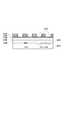
まず、図1に示すように、化合物半導体層を有する基板1010上に、エッチングストップ層1020と犠牲層1030とを介して、発光層1040を有する第1の部材1000を用意する。なお、1050は発光層上に必要に応じて設けることができる半導体多層膜(DBRミラー)である。なお、化合物半導体層を有する基板1010としては、例えばGaAs基板が挙げられるが、本発明はこれに限定されるものではなく、後述するように様々な基板の適用が可能である。 First, as shown in FIG. 1, a
次に、図2(a)に示される第2の部材2000を用意する。第2の部材は、例えばシリコンウエハやSOIウエハから構成される。図2(a)では、シリコン層2010上に有機絶縁膜2020が設けられている。また、図2(b)は、第2の部材の別の例を示している。図2(b)において、2000は第2の部材、2010はシリコン層、2020は有機絶縁層、2030は絶縁性の酸化膜、2050は駆動回路が設けられている領域である。ここでいうシリコン層には、シリコンウエハは勿論、シリコン層を有するウエハであればSOIウエハも含まれる。 Next, a
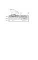
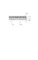
そして、シリコン層2010を含み構成されている第2の部材2000と、前記第1の部材1000とを、前記発光層1040が内側に位置するようにはり合わせて、はり合わせ構造体3000を形成する。この状態を図3に示す。また、2つの部材同士を貼り合せている様子を図4に示している。なお、図3では、第2の部材として、図2(b)に示した第2の部材を用いた場合を示しているが、勿論、図2(a)の第2の部材を用いることもできる。 Then, the
次に、図5に示すように、前記発光層1040が位置する側とは反対側から前記化合物半導体を有する基板1010をドライエッチングして、前記エッチングストップ層1020が露出するように前記化合物半導体層を有する基板に貫通溝5010を設ける。 Next, as shown in FIG. 5, the
基板1010のドライエッチングに代えて、ウエットエッチングを用いることもできるし、ドライエッチングで或る程度の深さまでエッチングした後、ウエットエッチングに切り換えて貫通溝を形成することもできる。いずれにせよ、前述のエッチングストップ層を基板1010の裏面側からのエッチングストップ層として機能するエッチング処理であれば特に限定されるものではない。 In place of dry etching of the
なお、この貫通溝5010を設けるに際して、予め、GaAsなどの基板1010の薄膜化(好ましくは100μm以下の厚さにするのがよい。)を行い、その後、レジストマスクパターンを用いて、前記貫通溝5010を形成することができる。 When providing the through
本発明に係る前記エッチングストップ層1020は、前記発光層1040側から前記基板1010に向かってエッチングする際にエッチングを所定の位置で止めるための層として用いているのではないことが特徴である。すなわち、前記基板1010側から前記発光層1040に向かって、ドライエッチングを行う際にエッチングを所定の位置でストップさせるための層として用いていることが特徴である。 The
更に、前記貫通溝の底部に前記犠牲層1030を露出させて(図6)、前記犠牲層をウェットエッチングすることにより、前記貫通溝5010が設けられた前記化合物半導体層を有する基板1010を前記はり合わせ構造体から除去する(図7)。 Further, the
こうして、シリコン層を含み構成される第2の部材上に発光層1040が移設される。 Thus, the
(第1の部材)
図1では、前記第1の部材1000が、前記化合物半導体層を有する基板1010上に、該化合物半導体層側から前記エッチングストップ層1020と前記犠牲層1030をこの順に有する場合を説明した。実際には、図8に示すように、該化合物半導体層側1010から前記犠牲層1030と前記エッチングストップ層1020をこの順に有するように構成することもできる。斯かる場合、はり合わせ構造体は、図9に示すようになる。そして、前記化合物半導体層を有する基板に貫通溝や貫通孔をドライエッチングによって設ける場合、図10に示すように、前記犠牲層1030も除去されて、前記エッチングストップ層1020が露出することになる。その後、前記犠牲層1030を除去することにより、はり合わせ構造体から前記化合物半導体層を有する基板が除去される。(First member)
In FIG. 1, the case where the
なお、発光層1040上に前記エッチングストップ層が残存する場合には、適宜それを除去することにより、図7のように、第2の部材上に前記発光層が移設されることになる。 When the etching stop layer remains on the
また、第1の部材に関しては、前記化合物半導体層を有する基板1010上に前記発光層1040がエピタキシャル成長できれば、前記犠牲層と前記エッチングストップ層との間に別な層が介在していてもよい。
前記化合物半導体層を有する基板としては、GaAs基板自体が挙げられる。As for the first member, another layer may be interposed between the sacrificial layer and the etching stop layer as long as the
An example of the substrate having the compound semiconductor layer is a GaAs substrate itself.
また、前記化合物半導体層を有する基板としては、表面にGaAs層を有するサファイア基板、表面にGaAs層を有するSiC基板、表面にGaAs層を有するZnO基板である。また、表面にGaAs層を有するGe基板、Siウエハ上にバッファー層を介してGaAs層を有するSi基板の適用も可能である。ここで、前記Siウエハ上にバッファー層を介してGaAs層を有する基板とは、Siウエハ上にSiGe層を介してGe層を有し、且つGe層上にGaAs層を有する基板である。 The substrate having the compound semiconductor layer is a sapphire substrate having a GaAs layer on the surface, a SiC substrate having a GaAs layer on the surface, and a ZnO substrate having a GaAs layer on the surface. Further, a Ge substrate having a GaAs layer on the surface and a Si substrate having a GaAs layer on a Si wafer via a buffer layer are also applicable. Here, the substrate having a GaAs layer on the Si wafer via a buffer layer is a substrate having a Ge layer on the Si wafer via a SiGe layer and a GaAs layer on the Ge layer.
ここで、図21には、前記化合物半導体層を有する基板として、Siウエハ上に、SiGe層、Ge層、及びGaAs層をこの順に積層して構成した例を示している。同図において、2910はシリコンウエハ、2915はSiGe層、2916はGe層である。2917は必ずしも必要ではないが、GaAs層である。1020はエッチングストップ層、1020は犠牲層、1040は発光層、1050は半導体多層膜(DBRミラー)である。なお、Siウエハ上に発光層を構成するGaAsは格子不整合性のため良質の膜として形成し難いといわれている。この格子不整合性を緩和する為に、Siウエハ上に、まずSiGe層を設け、その上にGe層を設けることで、発光層を構成する膜とその下地との格子定数を近づけることができる。また、SiGe層は、SixGe1−xとして、Siウエハ側はxを1に近くしておき、当該ウエハから離れるに従いxを小さくしていく、即ち、Geの量に勾配を設けることもできる。Here, FIG. 21 shows an example in which a SiGe layer, a Ge layer, and a GaAs layer are stacked in this order on a Si wafer as a substrate having the compound semiconductor layer. In this figure, 2910 is a silicon wafer, 2915 is a SiGe layer, and 2916 is a Ge layer. Although 2917 is not necessarily required, it is a GaAs layer.
更にまた、前記化合物半導体層を有する基板として、サファイア基板、SiC基板、ZnO基板の適用も可能である。 Furthermore, a sapphire substrate, a SiC substrate, or a ZnO substrate can be applied as the substrate having the compound semiconductor layer.
また、前記化合物半導体層を有する基板がGaAs基板である場合のエッチングストッパー層としては、GaInP(例えば、Ga0.5In0.5P)である。勿論、当該基板とエッチングストッパー層とのでエッチングの選択比が十分にとれるのであれば、特にエッチングストッパー層の材料は限定されるものではない。Further, when the substrate having the compound semiconductor layer is a GaAs substrate, the etching stopper layer is GaInP (for example, Ga0.5 In0.5 P). Needless to say, the material of the etching stopper layer is not particularly limited as long as the etching selectivity between the substrate and the etching stopper layer is sufficient.
(発光層)
前記発光層は、ダブルへテロ構造を用いることができるが、詳細は、実施例にて述べる。(Light emitting layer)
The light emitting layer can have a double hetero structure, and details will be described in Examples.
既述のように、前記発光層上に半導体多層膜ミラーを設けておくこともできる。 As described above, a semiconductor multilayer mirror can be provided on the light emitting layer.
(第2の部材)
前記第2の部材には、既述のように前記発光素子を駆動するための駆動回路を設けておくことができる。(Second member)
The second member may be provided with a drive circuit for driving the light emitting element as described above.
また、前記第2の部材を構成する前記シリコン層上には、表面を平坦化すると共に、前記第1の部材の接合層として機能する有機絶縁層を設けておくことが好適であるが、省略することもできる。 In addition, it is preferable to provide an organic insulating layer that planarizes the surface and functions as a bonding layer for the first member on the silicon layer that constitutes the second member. You can also
(メサエッチ)
前記除去工程後に、前記発光層がメサ形状になるようにエッチングする工程を有する。(Mesa etch)
After the removing step, there is a step of etching so that the light emitting layer has a mesa shape.
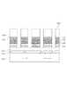
具体的には、第2の部材上に移設された発光層1040をいわゆるメサエッチング処理を行うとともに、該メサ形状の発光層1040上に絶縁膜2150を形成し、パターニングする(図11)。図11において、2210はシリコンウエハ、2230はパッシベーション膜、2220は有機絶縁層である。1050は発光層上に設けられている半導体多層膜である。図11では、電気的接続の為のコンタクトホール(2251から2254)が空けられている。次に、図12のように、前記コンタクトホールにメタル薄膜形成(2305、2306)を行い、駆動回路2299と発光層とが電気的に接続される。 Specifically, the light-emitting
なお、前記発光層がメサ形状あるいは島状になるようにエッチングした後、前記はり合わせ構造体を形成することもできる。斯かる場合、図13に示すように、空洞3500の存在するはり合わせ構造体が得られる。 The bonded structure can also be formed after the light emitting layer is etched to have a mesa shape or an island shape. In such a case, as shown in FIG. 13, a bonded structure having a
(マルチ)
なお、前記第1の部材は、図14に示すように、前記化合物半導体層を有する基板4010上に、該化合物半導体層側から第1の前記エッチングストップ層4020を形成する。更に、第1の前記発光層4040、前記犠牲層4030、第2の前記エッチングストップ層4021、及び第2の前記発光層4041を有するように構成することもできる。なお、4050と4051はそれぞれ必要に応じて設けることできる半導体多層膜(DBR)である。このように発光層を複数層設ける場合には、はり合わせ構造体は図15に示したようになる。所望のマスクを用いて、図16に示すようにGaAs等の基板4010を裏面側からドライエッチングする。第1のエッチングストップ層4020のところで、エッチングが止まることになるので、当該層が露出したら、塩酸などを用いたウェットエッチングにより除去する。そして、更に発光層側にドライエッチングを進めて、第2のエッチングストップ層4021を露出させる。(Multi)
As shown in FIG. 14, the first member forms the first
貫通溝を形成する場合には、図16に示すように前記第2のエッチングストップ層4021を露出させる。 When forming the through groove, the second
具体的には、化合物半導体層を有する基板4010にドライエッチングで孔や溝を設け、前記第1のエッチングストップ層4020を露出させ、当該層をウェットエッチングにより除去する。その後、更に、ドライエッチングで貫通溝を深堀し、前記第2のエッチングストップ層4021を露出させる。そして、貫通溝が形成されている前記化合物半導体層を有する基板4010に、接着層4097とUV剥離層4098とを介して前記貫通溝に接続する細孔を有するガラス支持体4099とはり合わせる(図17)。そして、図18に示すように前記犠牲層4030を除去することで、当該構造体からガラス支持体4099側が分離される。なお、GaAs基板4010が厚い場合には、CMPなどによる研磨や研削により当該基板の薄膜化(例えば100μm以下にする。)を行うのがよい。 Specifically, holes or grooves are provided by dry etching in the
その後、ガラス支持体4099側は、更に、別の基板5010(例えば駆動回路を有するシリコン層)上へ移設する為に、図19に示すようにはり合わせる。そして、図20に示すように、前記第1のエッチングストップ層4020を除去することにより、ガラス支持体4099側と、基板5010側とに分離する。発光層4040が基板5010上へ移設された後は、既述のプロセスにより、発光層に電流注入の為の電極を設けると共に、駆動回路と発光層とを電気的に接続する。 Thereafter, the
また、前記第1の部材は、以下の2つの発光層を有するように構成する。即ち、1つ目は、前記化合物半導体層を有する前記基板上に、該基板をエッチングする際にエッチングストッパーとして作用する第1の前記エッチングストップ層を介して設けられる第1の前記発光層である。2つ目は、前記犠牲層と第2のエッチングストップ層を介して設けられる第2の前記発光層である。 The first member is configured to have the following two light emitting layers. That is, the first is the first light emitting layer provided on the substrate having the compound semiconductor layer via the first etching stop layer that acts as an etching stopper when the substrate is etched. . The second is the second light emitting layer provided via the sacrificial layer and the second etching stop layer.
そして、前記犠牲層を除去することにより、前記第2の発光層を第2の部材に移設することになる。 Then, by removing the sacrificial layer, the second light emitting layer is transferred to the second member.
また、前記第1のエッチングストップ層を除去することにより、前記第1の発光層を他の部材に移設することができる。 Moreover, the first light emitting layer can be transferred to another member by removing the first etching stop layer.
ここで、前記犠牲層は例えば、AlAs層であり、前記第1及び第2のエッチングストップ層は例えばGaInPである。 Here, the sacrificial layer is, for example, an AlAs layer, and the first and second etching stop layers are, for example, GaInP.
なお、上述した発明において、第2の部材に移設するに先立って、ガラス基板等に一時的にはり合わせて、最後に第2の部材にはり合わせることもできる。 In the above-described invention, prior to transfer to the second member, it can be temporarily bonded to a glass substrate or the like, and finally to the second member.
(エッチング)
前記第1の部材を構成する基板に貫通溝を形成するエッチングをドライエッチング(RIBE)で行う場合のガス種としては、塩素系ガスとして、Cl2、SiCl4などがある。塩素系ガスにArなどの希ガスを混ぜて使用することも出来る。また、添加ガスとして、N2ガスやO2ガス、COガスなども適用できる。ドライエッチングの際のエッチングストッパー層としては、GaInP以外にも、例えばAlInPを用いることもできる。(etching)
Examples of the gas species in the case where the etching for forming the through groove in the substrate constituting the first member is performed by dry etching (RIBE) include Cl2 and SiCl4 as chlorine-based gases. It can also be used by mixing a rare gas such as Ar with a chlorine-based gas. Further, N2 gas, O2 gas, CO gas, or the like can be applied as the additive gas. As an etching stopper layer at the time of dry etching, for example, AlInP can be used in addition to GaInP.
なお、前記貫通溝を作製する場合にウェットエッチングを利用する場合には、以下のように行う。例えばGaInPをエッチングストッパー層として用い、GaAs基板をエッチングする場合は、硫酸系やリン酸系(これらには過酸化水素水が含まれている。)をエッチング液として用いる。また、InP系の基板をGaAs等をエッチングストッパー層として利用する場合には、塩素系のエッチング液を用いる。 In the case where wet etching is used when forming the through groove, the following process is performed. For example, when GaInP is used as an etching stopper layer and a GaAs substrate is etched, sulfuric acid or phosphoric acid (which contains hydrogen peroxide solution) is used as an etching solution. When an InP substrate is used as an etching stopper layer such as GaAs, a chlorine etching solution is used.
まず、第1の部材を作製するために、図1に示すように、p型GaAs基板1010を用意する。このGaAs基板が既述の化合物半導体層を有する基板に該当する。 First, in order to manufacture the first member, a p-
その上に、エッチングストップ層1020として、InGaP層をMOCVD法により100nm形成する。更に、犠牲層としてp−AlAs層1030を100nm形成する。なお、エッチングストップ層は、数nmから数十nmの厚さにすることもできる。 On top of that, an InGaP layer is formed as an
発光層1040は、基板側1010からp型コンタクト層(GaAs)、p型クラッド層、p型アクティブ層、n型クラッド層、n型コンタクト層(GaAs)、n−ストップ層(Ga0.5In0.5P)により構成される。このn−ストップ層とは、転写後にメサエッチを止めるための層である。
なお、p型クラッド層は、p−Al0.4Ga0.6As:350nmである。The
The p-type cladding layer is made of p-Al0 .4 Ga0.6 As: 350 nm.
活性層となるp型アクティブ層は、p−Al0.13Ga0.87As:300nmである。n型クラッド層は、n−Al0.23Ga0.77As:1300nmである。
p型、n型ともに、コンタクト層の厚さは、200nmである。The p-type active layer serving as the active layer is p-Al0 .13 Ga0.87 As: 300 nm. The n-type cladding layer is made of n-Al0 .23 Ga0.77 As: 1300 nm.
For both p-type and n-type, the thickness of the contact layer is 200 nm.
また、n型DBR層(図1の1050)として、Al0.2Ga0.8As:633Å/Al0.8Ga0.2As:565Åの組を20ペア積層して構成している。Further, as the n-type DBR layer (1050 in FIG. 1), 20 pairs of Al0.2 Ga0.8 As: 633 Å / Al0.8 Ga0.2 As: 565 積 層 are stacked.
第2の部材2000(図2)としては、シリコン層上にスピンコートで平坦に塗布が可能で、犠牲層を選択エッチングする際に、エッチングされないポリマー膜である有機絶縁膜を設けておく。有機絶縁膜としては、溶剤に融解したポリイミドをスピンコートし、溶剤を蒸発させることで2μmの厚みのポリイミド膜を用いることができる。 As the second member 2000 (FIG. 2), an organic insulating film that is a polymer film that is not etched when a sacrificial layer is selectively etched can be provided on a silicon layer by spin coating. As the organic insulating film, a polyimide film having a thickness of 2 μm can be used by spin-coating polyimide melted in a solvent and evaporating the solvent.
はり合わせ工程(図3)を行う際には、窒素、酸素、アルゴンなどのプラズマに晒して表面活性化処理をするとともに、はり合わせ後に400℃以下の低温熱処理(例えば、280℃、2時間)を行う。低温ではり合わせを行うことは下部にシリコントランジスタなどの駆動素子がある場合に必須であり、高温で処理するとシリコン素子の不純物が再拡散して、素子が正常に動作しない可能性が高まる。 When performing the bonding step (FIG. 3), the surface activation treatment is performed by exposure to plasma such as nitrogen, oxygen, and argon, and a low temperature heat treatment at 400 ° C. or lower (eg, 280 ° C., 2 hours) after bonding. I do. Bonding at a low temperature is indispensable when there is a driving element such as a silicon transistor in the lower part, and if it is processed at a high temperature, impurities in the silicon element are re-diffused and the possibility that the element does not operate normally increases.
はり合わせ工程後に、図5に示すように、GaAs基板の裏面にレジストマスクを塗布、感光して、所望の位置に、所望の開口を形成し、ICP−RIE:容量結合プラズマ装置によって、ドライエッチングにより、貫通溝(図5の5010)を形成する。ドライエッチング用のレジスト膜塗布に先だって、CMPなどによるGaAs基板の薄膜化を行うことが好ましい。RIEの条件としては、基板温度は100℃程度で反応性ガスとしては塩素を用いて行う。本実施例においては、前記ドライエッチング処理時に、前記エッチングストップ層InGaP1020で止まることを利用する。 After the bonding process, as shown in FIG. 5, a resist mask is applied to the back surface of the GaAs substrate and exposed to form a desired opening at a desired position, and dry etching is performed by an ICP-RIE: capacitively coupled plasma apparatus. Thus, a through groove (5010 in FIG. 5) is formed. Prior to applying a resist film for dry etching, it is preferable to thin the GaAs substrate by CMP or the like. As the RIE conditions, the substrate temperature is about 100 ° C., and chlorine is used as the reactive gas. In this embodiment, it is used that the etching stops at the etching stop layer InGaP1020 during the dry etching process.
その後、InGaPエッチングストップ層をHClを用いて除去するとAlAs犠牲層を露出させる。この犠牲層であるAlAs層は、稀HFで選択的にエッチング除去し、はり合わせ構造体からGaAs基板を分離する。AlAs層の除去は、5%フッ酸溶液を用いて行うことができる。 Thereafter, when the InGaP etching stop layer is removed using HCl, the AlAs sacrificial layer is exposed. This sacrificial AlAs layer is selectively etched away with rare HF to separate the GaAs substrate from the bonded structure. The removal of the AlAs layer can be performed using a 5% hydrofluoric acid solution.
その後、シリコン層上に移設された発光層1040は、図11、12に示すように、メサ形状にエッチング処理するとともに、プラズマCVDによりSiN膜2150を形成する。その後、SiN膜をパターニングして、コンタクトホール2251等を形成し、Ni/Auなどのメタル蒸着を行い、発光層(発光ダイオード)と駆動回路2299とを電気的に接続する。電気的な接続に際しては、図11の半導体多層膜をn型DBRとして構成することにより、駆動回路とこのn型DBR層とを電気的に接続することができる。斯かる構成にしておけば、DBRの層厚方向の全体にn側電極からキャリアを注入せずに済むので、高抵抗化を回避できる。 Thereafter, the
本発明に係る発光素子の製造方法を用いて、シリコン層上に発光素子をアレイ状に形成できる。当該アレイ状の発光素子は、LEDプリンタのプリンタヘッドを構成することできる。 By using the method for manufacturing a light-emitting element according to the present invention, the light-emitting elements can be formed in an array on the silicon layer. The array of light emitting elements can constitute a printer head of an LED printer.
1010 化合物半導体層を有する基板
1020 エッチングストップ層
1030 犠牲層
1040 発光層
1050 半導体多層膜1010 substrate having
Claims (13)
Translated fromJapanese化合物半導体層を有する基板上に、エッチングストップ層と犠牲層とを介して、発光層を有する第1の部材を用意する工程、
シリコン層を含み構成されている第2の部材と、前記第1の部材とを、前記発光層が内側に位置するようにはり合わせて、はり合わせ構造体を形成する工程、
前記第1の部材を、前記発光層側とは反対側からエッチングして、前記エッチングストップ層が露出するように前記基板に貫通溝を設ける工程、及び
前記犠牲層をエッチングすることにより、前記貫通溝が設けられた前記基板を前記はり合わせ構造体から除去する除去工程、
を有することを特徴とする発光素子の製造方法。A method of manufacturing a light emitting device,
Preparing a first member having a light emitting layer on a substrate having a compound semiconductor layer via an etching stop layer and a sacrificial layer;
A step of bonding a second member including a silicon layer and the first member so that the light emitting layer is located inside to form a bonded structure;
Etching the first member from the side opposite to the light emitting layer side to provide a through groove in the substrate so that the etching stop layer is exposed, and etching the sacrificial layer to thereby pass through the sacrificial layer. A removing step of removing the substrate provided with the groove from the bonded structure;
A method for manufacturing a light-emitting element, comprising:
前記化合物半導体層を有する前記基板上に、該基板をエッチングする際にエッチングストッパーとして作用する第1の前記エッチングストップ層を介して第1の前記発光層を有し、且つ
前記犠牲層と第2のエッチングストップ層を介して、第2の前記発光層を有し構成されており、
前記犠牲層を除去することにより、前記第2の発光層を第2の部材に移設し、
前記第1のエッチングストップ層を除去することにより、前記第1の発光層を他の部材に移設することを特徴とする請求項1から11記載の発光素子の製造方法。The first member is
On the substrate having the compound semiconductor layer, the first light emitting layer is provided via the first etching stop layer acting as an etching stopper when the substrate is etched, and the sacrificial layer and the second layer The second light emitting layer is configured through the etching stop layer of
By removing the sacrificial layer, the second light emitting layer is transferred to the second member,
12. The method of manufacturing a light emitting element according to claim 1, wherein the first light emitting layer is transferred to another member by removing the first etching stop layer.
Priority Applications (7)
| Application Number | Priority Date | Filing Date | Title |
|---|---|---|---|
| JP2007261018AJP2009094144A (en) | 2007-10-04 | 2007-10-04 | Method for manufacturing light emitting device |
| PCT/JP2008/068254WO2009044923A1 (en) | 2007-10-04 | 2008-10-01 | Method for manufacturing light emitting device |
| US12/669,790US20100197054A1 (en) | 2007-10-04 | 2008-10-01 | Method for manufacturing light emitting device |
| EP08835326AEP2171758B1 (en) | 2007-10-04 | 2008-10-01 | Method of manufacturing light-emitting device |
| KR1020107009059AKR101065990B1 (en) | 2007-10-04 | 2008-10-01 | Manufacturing method of light emitting device |
| CN2008801095923ACN101816072B (en) | 2007-10-04 | 2008-10-01 | Method for manufacturing light emitting device |
| TW097137752ATWI395347B (en) | 2007-10-04 | 2008-10-01 | Method of manufacturing a light-emitting device |
Applications Claiming Priority (1)
| Application Number | Priority Date | Filing Date | Title |
|---|---|---|---|
| JP2007261018AJP2009094144A (en) | 2007-10-04 | 2007-10-04 | Method for manufacturing light emitting device |
Publications (1)
| Publication Number | Publication Date |
|---|---|
| JP2009094144Atrue JP2009094144A (en) | 2009-04-30 |
Family
ID=40227758
Family Applications (1)
| Application Number | Title | Priority Date | Filing Date |
|---|---|---|---|
| JP2007261018APendingJP2009094144A (en) | 2007-10-04 | 2007-10-04 | Method for manufacturing light emitting device |
Country Status (7)
| Country | Link |
|---|---|
| US (1) | US20100197054A1 (en) |
| EP (1) | EP2171758B1 (en) |
| JP (1) | JP2009094144A (en) |
| KR (1) | KR101065990B1 (en) |
| CN (1) | CN101816072B (en) |
| TW (1) | TWI395347B (en) |
| WO (1) | WO2009044923A1 (en) |
Cited By (9)
| Publication number | Priority date | Publication date | Assignee | Title |
|---|---|---|---|---|
| JP2013542589A (en)* | 2010-09-10 | 2013-11-21 | バーレイス テクノロジーズ エルエルシー | Method of manufacturing an optoelectronic device using a layer separated from a semiconductor donor and device manufactured thereby |
| KR101396281B1 (en) | 2010-10-04 | 2014-05-16 | 에피스타 코포레이션 | A light-emitting element having a plurality of contact parts |
| JP2016522992A (en)* | 2013-05-16 | 2016-08-04 | オスラム オプト セミコンダクターズ ゲゼルシャフト ミット ベシュレンクテル ハフツングOsram Opto Semiconductors GmbH | Method for manufacturing an optoelectronic semiconductor chip |
| JP2019075569A (en)* | 2018-12-12 | 2019-05-16 | 晶元光電股▲ふん▼有限公司Epistar Corporation | Method of selectively transferring semiconductor element |
| WO2020196271A1 (en)* | 2019-03-22 | 2020-10-01 | 日亜化学工業株式会社 | Method for manufacturing image display device and image display device |
| JPWO2020226044A1 (en)* | 2019-05-08 | 2020-11-12 | ||
| WO2021014972A1 (en)* | 2019-07-25 | 2021-01-28 | 日亜化学工業株式会社 | Image display device manufacturing method and image display device |
| JPWO2021065918A1 (en)* | 2019-10-01 | 2021-04-08 | ||
| US20230136686A1 (en)* | 2020-03-23 | 2023-05-04 | Sony Semiconductor Solutions Corporation | Semiconductor device and manufacturing method of same |
Families Citing this family (12)
| Publication number | Priority date | Publication date | Assignee | Title |
|---|---|---|---|---|
| TWI411129B (en) | 2009-12-31 | 2013-10-01 | Epistar Corp | Method for forming light-emitting diode |
| TWI429795B (en)* | 2011-10-31 | 2014-03-11 | Univ Nat Taiwan | Method for producing zinc oxide on gallium nitride and its application THEREOF |
| CN103296155B (en)* | 2013-06-06 | 2016-04-20 | 刘凤全 | A kind of manufacture method of thin-film LED epitaxial chip |
| TWI671141B (en) | 2013-08-30 | 2019-09-11 | 半導體能源研究所股份有限公司 | Support supply apparatus and method for supplying support |
| CN105097430B (en)* | 2014-05-05 | 2019-06-28 | 中芯国际集成电路制造(上海)有限公司 | A kind of manufacturing method of semiconductor devices |
| US10804407B2 (en) | 2016-05-12 | 2020-10-13 | Semiconductor Energy Laboratory Co., Ltd. | Laser processing apparatus and stack processing apparatus |
| KR102634586B1 (en)* | 2018-06-11 | 2024-02-07 | 삼성디스플레이 주식회사 | Light emitting element, method of manufacturing the same and display device comprising the light emitting element |
| KR102590984B1 (en) | 2018-10-30 | 2023-10-18 | 삼성디스플레이 주식회사 | Light emitting element structure and method of fabricating a light emitting element |
| JP7484078B2 (en)* | 2019-05-10 | 2024-05-16 | 日亜化学工業株式会社 | Image display device manufacturing method and image display device |
| CN113994486A (en)* | 2019-05-10 | 2022-01-28 | 日亚化学工业株式会社 | Manufacturing method of image display device and image display device |
| CN110854154B (en)* | 2019-11-18 | 2024-04-30 | 佛山市国星半导体技术有限公司 | Silicon-based micro LED chip and manufacturing method thereof |
| CN117855339B (en)* | 2024-03-05 | 2024-05-14 | 山西创芯光电科技有限公司 | Preparation method of superlattice infrared detector with substrate completely removed |
Citations (4)
| Publication number | Priority date | Publication date | Assignee | Title |
|---|---|---|---|---|
| JPH07106632A (en)* | 1993-09-30 | 1995-04-21 | Victor Co Of Japan Ltd | Semiconductor light emitting element array |
| JP2004179641A (en)* | 2002-11-11 | 2004-06-24 | Oki Data Corp | Semiconductor device, optical print head, and image forming apparatus |
| JP2005072422A (en)* | 2003-08-27 | 2005-03-17 | Nec Corp | Epitaxial layer separation method for semiconductor device |
| WO2007025497A1 (en)* | 2005-09-01 | 2007-03-08 | Osram Opto Semiconductors Gmbh | Method for laterally cutting through a semiconductor wafer and optoelectronic component |
Family Cites Families (42)
| Publication number | Priority date | Publication date | Assignee | Title |
|---|---|---|---|---|
| US5750000A (en)* | 1990-08-03 | 1998-05-12 | Canon Kabushiki Kaisha | Semiconductor member, and process for preparing same and semiconductor device formed by use of same |
| EP0747935B1 (en)* | 1990-08-03 | 2004-02-04 | Canon Kabushiki Kaisha | Process for preparing an SOI-member |
| JP2693032B2 (en)* | 1990-10-16 | 1997-12-17 | キヤノン株式会社 | Method for forming semiconductor layer and method for manufacturing solar cell using the same |
| CA2069038C (en)* | 1991-05-22 | 1997-08-12 | Kiyofumi Sakaguchi | Method for preparing semiconductor member |
| EP0534474B1 (en)* | 1991-09-27 | 2002-01-16 | Canon Kabushiki Kaisha | Method of processing a silicon substrate |
| JP3192000B2 (en)* | 1992-08-25 | 2001-07-23 | キヤノン株式会社 | Semiconductor substrate and manufacturing method thereof |
| JP3352118B2 (en)* | 1992-08-25 | 2002-12-03 | キヤノン株式会社 | Semiconductor device and manufacturing method thereof |
| JPH06244389A (en)* | 1992-12-25 | 1994-09-02 | Canon Inc | Manufacture of semiconductor substrate and semiconductor substrate manufactured by this method |
| JPH09331049A (en)* | 1996-04-08 | 1997-12-22 | Canon Inc | Method for manufacturing bonded SOI substrate and SOI substrate |
| US6756289B1 (en)* | 1996-12-27 | 2004-06-29 | Canon Kabushiki Kaisha | Method of producing semiconductor member and method of producing solar cell |
| DE69738307T2 (en)* | 1996-12-27 | 2008-10-02 | Canon K.K. | Manufacturing method of a semiconductor device and manufacturing method of a solar cell |
| CA2231625C (en)* | 1997-03-17 | 2002-04-02 | Canon Kabushiki Kaisha | Semiconductor substrate having compound semiconductor layer, process for its production, and electronic device fabricated on semiconductor substrate |
| CA2232796C (en)* | 1997-03-26 | 2002-01-22 | Canon Kabushiki Kaisha | Thin film forming process |
| CA2233115C (en)* | 1997-03-27 | 2002-03-12 | Canon Kabushiki Kaisha | Semiconductor substrate and method of manufacturing the same |
| JP3647191B2 (en)* | 1997-03-27 | 2005-05-11 | キヤノン株式会社 | Manufacturing method of semiconductor device |
| SG68035A1 (en)* | 1997-03-27 | 1999-10-19 | Canon Kk | Method and apparatus for separating composite member using fluid |
| JP3492142B2 (en)* | 1997-03-27 | 2004-02-03 | キヤノン株式会社 | Manufacturing method of semiconductor substrate |
| US6306729B1 (en)* | 1997-12-26 | 2001-10-23 | Canon Kabushiki Kaisha | Semiconductor article and method of manufacturing the same |
| US6331208B1 (en)* | 1998-05-15 | 2001-12-18 | Canon Kabushiki Kaisha | Process for producing solar cell, process for producing thin-film semiconductor, process for separating thin-film semiconductor, and process for forming semiconductor |
| JP3697106B2 (en)* | 1998-05-15 | 2005-09-21 | キヤノン株式会社 | Method for manufacturing semiconductor substrate and method for manufacturing semiconductor thin film |
| US6391743B1 (en)* | 1998-09-22 | 2002-05-21 | Canon Kabushiki Kaisha | Method and apparatus for producing photoelectric conversion device |
| TW400393B (en)* | 1999-02-12 | 2000-08-01 | Taiwan Semiconductor Mfg | The metalization process of utilizing the sacrifice layer to avoid the damage of the etch stopping layer |
| US6452091B1 (en)* | 1999-07-14 | 2002-09-17 | Canon Kabushiki Kaisha | Method of producing thin-film single-crystal device, solar cell module and method of producing the same |
| JP2001284622A (en)* | 2000-03-31 | 2001-10-12 | Canon Inc | Semiconductor member manufacturing method and solar cell manufacturing method |
| JP2002359247A (en)* | 2000-07-10 | 2002-12-13 | Canon Inc | Semiconductor member, semiconductor device, and manufacturing method thereof |
| DE60124766T2 (en)* | 2000-08-04 | 2007-10-11 | Amberwave Systems Corp. | SILICON WAIST WITH MONOLITHIC OPTOELECTRONIC COMPONENTS |
| JP4708577B2 (en)* | 2001-01-31 | 2011-06-22 | キヤノン株式会社 | Method for manufacturing thin film semiconductor device |
| JP4803884B2 (en)* | 2001-01-31 | 2011-10-26 | キヤノン株式会社 | Method for manufacturing thin film semiconductor device |
| JP2002229473A (en)* | 2001-01-31 | 2002-08-14 | Canon Inc | Display device manufacturing method |
| JP4211256B2 (en)* | 2001-12-28 | 2009-01-21 | セイコーエプソン株式会社 | Semiconductor integrated circuit, semiconductor integrated circuit manufacturing method, electro-optical device, and electronic apparatus |
| US7180099B2 (en)* | 2002-11-11 | 2007-02-20 | Oki Data Corporation | Semiconductor apparatus with thin semiconductor film |
| JP4097510B2 (en)* | 2002-11-20 | 2008-06-11 | 株式会社沖データ | Manufacturing method of semiconductor device |
| WO2004099473A1 (en)* | 2003-05-06 | 2004-11-18 | Canon Kabushiki Kaisha | Semiconductor substrate, semiconductor device, light emitting diode and producing method therefor |
| JP2004335642A (en)* | 2003-05-06 | 2004-11-25 | Canon Inc | Substrate and manufacturing method thereof |
| JP2005005509A (en)* | 2003-06-12 | 2005-01-06 | Canon Inc | Thin film transistor and manufacturing method thereof |
| US6913985B2 (en)* | 2003-06-20 | 2005-07-05 | Oki Data Corporation | Method of manufacturing a semiconductor device |
| KR101063646B1 (en)* | 2004-03-19 | 2011-09-07 | 엘지전자 주식회사 | Light emitting element and manufacturing method thereof |
| JP4771510B2 (en)* | 2004-06-23 | 2011-09-14 | キヤノン株式会社 | Semiconductor layer manufacturing method and substrate manufacturing method |
| JP4950047B2 (en)* | 2004-07-22 | 2012-06-13 | ボード オブ トラスティーズ オブ ザ レランド スタンフォード ジュニア ユニバーシティ | Method for growing germanium and method for manufacturing semiconductor substrate |
| JP4854336B2 (en)* | 2006-03-07 | 2012-01-18 | キヤノン株式会社 | Manufacturing method of substrate for inkjet head |
| WO2007133044A1 (en)* | 2006-05-15 | 2007-11-22 | Epivalley Co., Ltd. | Manufacturing method of nitride semiconductor substrate and iii-nitride semiconductor light emitting device |
| JP5171016B2 (en)* | 2006-10-27 | 2013-03-27 | キヤノン株式会社 | Semiconductor member, manufacturing method of semiconductor article, and LED array using the manufacturing method |
- 2007
- 2007-10-04JPJP2007261018Apatent/JP2009094144A/enactivePending
- 2008
- 2008-10-01KRKR1020107009059Apatent/KR101065990B1/ennot_activeExpired - Fee Related
- 2008-10-01CNCN2008801095923Apatent/CN101816072B/ennot_activeExpired - Fee Related
- 2008-10-01EPEP08835326Apatent/EP2171758B1/ennot_activeNot-in-force
- 2008-10-01USUS12/669,790patent/US20100197054A1/ennot_activeAbandoned
- 2008-10-01TWTW097137752Apatent/TWI395347B/ennot_activeIP Right Cessation
- 2008-10-01WOPCT/JP2008/068254patent/WO2009044923A1/enactiveApplication Filing
Patent Citations (4)
| Publication number | Priority date | Publication date | Assignee | Title |
|---|---|---|---|---|
| JPH07106632A (en)* | 1993-09-30 | 1995-04-21 | Victor Co Of Japan Ltd | Semiconductor light emitting element array |
| JP2004179641A (en)* | 2002-11-11 | 2004-06-24 | Oki Data Corp | Semiconductor device, optical print head, and image forming apparatus |
| JP2005072422A (en)* | 2003-08-27 | 2005-03-17 | Nec Corp | Epitaxial layer separation method for semiconductor device |
| WO2007025497A1 (en)* | 2005-09-01 | 2007-03-08 | Osram Opto Semiconductors Gmbh | Method for laterally cutting through a semiconductor wafer and optoelectronic component |
Cited By (27)
| Publication number | Priority date | Publication date | Assignee | Title |
|---|---|---|---|---|
| JP2013542589A (en)* | 2010-09-10 | 2013-11-21 | バーレイス テクノロジーズ エルエルシー | Method of manufacturing an optoelectronic device using a layer separated from a semiconductor donor and device manufactured thereby |
| US9269854B2 (en) | 2010-09-10 | 2016-02-23 | VerLASE TECHNOLOGIES LLC | Methods of fabricating optoelectronic devices using layers detached from semiconductor donors and devices made thereby |
| US9525150B2 (en) | 2010-09-10 | 2016-12-20 | VerLASE TECHNOLOGIES LLC | Optoelectronic devices made using layers detached from inherently lamellar semiconductor donors |
| KR101763984B1 (en) | 2010-09-10 | 2017-08-01 | 베르라세 테크놀러지스 엘엘씨 | Methods of fabricating optoelectronic devices using layers detached from semiconductor donors and devices made thereby |
| KR101396281B1 (en) | 2010-10-04 | 2014-05-16 | 에피스타 코포레이션 | A light-emitting element having a plurality of contact parts |
| JP2016522992A (en)* | 2013-05-16 | 2016-08-04 | オスラム オプト セミコンダクターズ ゲゼルシャフト ミット ベシュレンクテル ハフツングOsram Opto Semiconductors GmbH | Method for manufacturing an optoelectronic semiconductor chip |
| US9799801B2 (en) | 2013-05-16 | 2017-10-24 | Osram Opto Semiconductors Gmbh | Method for producing an optoelectronic semiconductor chip |
| JP2019075569A (en)* | 2018-12-12 | 2019-05-16 | 晶元光電股▲ふん▼有限公司Epistar Corporation | Method of selectively transferring semiconductor element |
| JP7594231B2 (en) | 2019-03-22 | 2024-12-04 | 日亜化学工業株式会社 | Manufacturing method of image display device |
| JPWO2020196271A1 (en)* | 2019-03-22 | 2020-10-01 | ||
| KR102816943B1 (en)* | 2019-03-22 | 2025-06-04 | 니치아 카가쿠 고교 가부시키가이샤 | Method for manufacturing a video display device and a video display device |
| WO2020196271A1 (en)* | 2019-03-22 | 2020-10-01 | 日亜化学工業株式会社 | Method for manufacturing image display device and image display device |
| JP2024088732A (en)* | 2019-03-22 | 2024-07-02 | 日亜化学工業株式会社 | Manufacturing method of image display device |
| KR20210143729A (en)* | 2019-03-22 | 2021-11-29 | 니치아 카가쿠 고교 가부시키가이샤 | Method for manufacturing an image display device and an image display device |
| US11476308B2 (en) | 2019-03-22 | 2022-10-18 | Nichia Corporation | Method for manufacturing image display device and image display device |
| JP7507373B2 (en) | 2019-03-22 | 2024-06-28 | 日亜化学工業株式会社 | Image display device manufacturing method and image display device |
| JPWO2020226044A1 (en)* | 2019-05-08 | 2020-11-12 | ||
| JP7457255B2 (en) | 2019-05-08 | 2024-03-28 | 日亜化学工業株式会社 | Image display device manufacturing method and image display device |
| JPWO2021014972A1 (en)* | 2019-07-25 | 2021-01-28 | ||
| JP7428919B2 (en) | 2019-07-25 | 2024-02-07 | 日亜化学工業株式会社 | Image display device manufacturing method and image display device |
| TWI877185B (en)* | 2019-07-25 | 2025-03-21 | 日商日亞化學工業股份有限公司 | Method for manufacturing image display device and image display device |
| US12310145B2 (en) | 2019-07-25 | 2025-05-20 | Nichia Corporation | Image display device manufacturing method and image display device |
| WO2021014972A1 (en)* | 2019-07-25 | 2021-01-28 | 日亜化学工業株式会社 | Image display device manufacturing method and image display device |
| JP7489605B2 (en) | 2019-10-01 | 2024-05-24 | 日亜化学工業株式会社 | Image display device manufacturing method and image display device |
| WO2021065918A1 (en)* | 2019-10-01 | 2021-04-08 | 日亜化学工業株式会社 | Method for manufacturing image display device and image display device |
| JPWO2021065918A1 (en)* | 2019-10-01 | 2021-04-08 | ||
| US20230136686A1 (en)* | 2020-03-23 | 2023-05-04 | Sony Semiconductor Solutions Corporation | Semiconductor device and manufacturing method of same |
Also Published As
| Publication number | Publication date |
|---|---|
| KR101065990B1 (en) | 2011-09-19 |
| EP2171758A1 (en) | 2010-04-07 |
| KR20100063128A (en) | 2010-06-10 |
| CN101816072B (en) | 2012-04-25 |
| TW200931685A (en) | 2009-07-16 |
| EP2171758B1 (en) | 2012-08-01 |
| US20100197054A1 (en) | 2010-08-05 |
| WO2009044923A1 (en) | 2009-04-09 |
| CN101816072A (en) | 2010-08-25 |
| TWI395347B (en) | 2013-05-01 |
Similar Documents
| Publication | Publication Date | Title |
|---|---|---|
| JP2009094144A (en) | Method for manufacturing light emitting device | |
| JP4771510B2 (en) | Semiconductor layer manufacturing method and substrate manufacturing method | |
| JP4827698B2 (en) | Method for forming light emitting element | |
| JP6680790B2 (en) | Hybrid heterostructure light emitting device | |
| CN118160065A (en) | Method for manufacturing bonded semiconductor wafer | |
| JP2005012188A (en) | Manufacturing method of semiconductor device | |
| US20090239324A1 (en) | Method for manufacturing semiconductor device using separable support body | |
| US12068166B2 (en) | Semiconductor substrate | |
| US11698488B2 (en) | Method for fabricating a heterostructure comprising active or passive elementary structure made of III-V material on the surface of a silicon-based substrate | |
| US9799801B2 (en) | Method for producing an optoelectronic semiconductor chip | |
| KR20140128672A (en) | Method of recycling a substrate | |
| US8368111B2 (en) | Semiconductor light emitting device and method for manufacturing thereof | |
| CN101527427B (en) | Manufacturing method of semiconductor optical element | |
| JP4638000B2 (en) | Manufacturing method of semiconductor substrate | |
| KR102844644B1 (en) | Semiconductor substrate, method for manufacturing semiconductor substrate, device for manufacturing semiconductor substrate, electronic component and electronic device | |
| JP2009283762A (en) | Method for manufacturing nitride compound semiconductor led | |
| JP4827655B2 (en) | Semiconductor light emitting device and manufacturing method thereof | |
| TW202414515A (en) | Method for producing bonded wafer for micro LEDS | |
| US20090155942A1 (en) | Hybrid metal bonded vertical cavity surface emitting laser and fabricating method thereof | |
| JP7687146B2 (en) | Semiconductor optical device and its manufacturing method | |
| CN101826585A (en) | Semiconductor light emitting element and manufacturing method thereof | |
| JP2011049565A (en) | Method of manufacturing semiconductor substrate | |
| JP5674692B2 (en) | Nitride semiconductor device and method for manufacturing nitride semiconductor device | |
| JP2006287120A (en) | Light emitting device and manufacturing method thereof | |
| CN114864757A (en) | Vertical light emitting diode and manufacturing method thereof |
Legal Events
| Date | Code | Title | Description |
|---|---|---|---|
| RD04 | Notification of resignation of power of attorney | Free format text:JAPANESE INTERMEDIATE CODE: A7424 Effective date:20100201 | |
| RD01 | Notification of change of attorney | Free format text:JAPANESE INTERMEDIATE CODE: A7421 Effective date:20100630 | |
| A621 | Written request for application examination | Free format text:JAPANESE INTERMEDIATE CODE: A621 Effective date:20101001 | |
| A977 | Report on retrieval | Free format text:JAPANESE INTERMEDIATE CODE: A971007 Effective date:20130424 | |
| A131 | Notification of reasons for refusal | Free format text:JAPANESE INTERMEDIATE CODE: A131 Effective date:20130430 | |
| A02 | Decision of refusal | Free format text:JAPANESE INTERMEDIATE CODE: A02 Effective date:20130917 |