JP2009093154A - Display device and manufacturing method of display device - Google Patents
Display device and manufacturing method of display deviceDownload PDFInfo
- Publication number
- JP2009093154A JP2009093154AJP2008216975AJP2008216975AJP2009093154AJP 2009093154 AJP2009093154 AJP 2009093154AJP 2008216975 AJP2008216975 AJP 2008216975AJP 2008216975 AJP2008216975 AJP 2008216975AJP 2009093154 AJP2009093154 AJP 2009093154A
- Authority
- JP
- Japan
- Prior art keywords
- active layer
- layer
- forming
- semiconductor film
- display device
- Prior art date
- Legal status (The legal status is an assumption and is not a legal conclusion. Google has not performed a legal analysis and makes no representation as to the accuracy of the status listed.)
- Granted
Links
Images


Classifications
- G—PHYSICS
- G02—OPTICS
- G02F—OPTICAL DEVICES OR ARRANGEMENTS FOR THE CONTROL OF LIGHT BY MODIFICATION OF THE OPTICAL PROPERTIES OF THE MEDIA OF THE ELEMENTS INVOLVED THEREIN; NON-LINEAR OPTICS; FREQUENCY-CHANGING OF LIGHT; OPTICAL LOGIC ELEMENTS; OPTICAL ANALOGUE/DIGITAL CONVERTERS
- G02F1/00—Devices or arrangements for the control of the intensity, colour, phase, polarisation or direction of light arriving from an independent light source, e.g. switching, gating or modulating; Non-linear optics
- G02F1/01—Devices or arrangements for the control of the intensity, colour, phase, polarisation or direction of light arriving from an independent light source, e.g. switching, gating or modulating; Non-linear optics for the control of the intensity, phase, polarisation or colour
- G02F1/13—Devices or arrangements for the control of the intensity, colour, phase, polarisation or direction of light arriving from an independent light source, e.g. switching, gating or modulating; Non-linear optics for the control of the intensity, phase, polarisation or colour based on liquid crystals, e.g. single liquid crystal display cells
- G02F1/133—Constructional arrangements; Operation of liquid crystal cells; Circuit arrangements
- G02F1/136—Liquid crystal cells structurally associated with a semi-conducting layer or substrate, e.g. cells forming part of an integrated circuit
- G02F1/1362—Active matrix addressed cells
- G02F1/1368—Active matrix addressed cells in which the switching element is a three-electrode device
- G—PHYSICS
- G06—COMPUTING OR CALCULATING; COUNTING
- G06F—ELECTRIC DIGITAL DATA PROCESSING
- G06F3/00—Input arrangements for transferring data to be processed into a form capable of being handled by the computer; Output arrangements for transferring data from processing unit to output unit, e.g. interface arrangements
- G06F3/01—Input arrangements or combined input and output arrangements for interaction between user and computer
- G06F3/03—Arrangements for converting the position or the displacement of a member into a coded form
- G06F3/041—Digitisers, e.g. for touch screens or touch pads, characterised by the transducing means
- G06F3/0412—Digitisers structurally integrated in a display
- G—PHYSICS
- G06—COMPUTING OR CALCULATING; COUNTING
- G06F—ELECTRIC DIGITAL DATA PROCESSING
- G06F3/00—Input arrangements for transferring data to be processed into a form capable of being handled by the computer; Output arrangements for transferring data from processing unit to output unit, e.g. interface arrangements
- G06F3/01—Input arrangements or combined input and output arrangements for interaction between user and computer
- G06F3/03—Arrangements for converting the position or the displacement of a member into a coded form
- G06F3/041—Digitisers, e.g. for touch screens or touch pads, characterised by the transducing means
- G06F3/042—Digitisers, e.g. for touch screens or touch pads, characterised by the transducing means by opto-electronic means
- G06F3/0421—Digitisers, e.g. for touch screens or touch pads, characterised by the transducing means by opto-electronic means by interrupting or reflecting a light beam, e.g. optical touch-screen
- G—PHYSICS
- G09—EDUCATION; CRYPTOGRAPHY; DISPLAY; ADVERTISING; SEALS
- G09F—DISPLAYING; ADVERTISING; SIGNS; LABELS OR NAME-PLATES; SEALS
- G09F9/00—Indicating arrangements for variable information in which the information is built-up on a support by selection or combination of individual elements
- G09F9/30—Indicating arrangements for variable information in which the information is built-up on a support by selection or combination of individual elements in which the desired character or characters are formed by combining individual elements
- H—ELECTRICITY
- H10—SEMICONDUCTOR DEVICES; ELECTRIC SOLID-STATE DEVICES NOT OTHERWISE PROVIDED FOR
- H10D—INORGANIC ELECTRIC SEMICONDUCTOR DEVICES
- H10D86/00—Integrated devices formed in or on insulating or conducting substrates, e.g. formed in silicon-on-insulator [SOI] substrates or on stainless steel or glass substrates
- H10D86/40—Integrated devices formed in or on insulating or conducting substrates, e.g. formed in silicon-on-insulator [SOI] substrates or on stainless steel or glass substrates characterised by multiple TFTs
- H10D86/421—Integrated devices formed in or on insulating or conducting substrates, e.g. formed in silicon-on-insulator [SOI] substrates or on stainless steel or glass substrates characterised by multiple TFTs having a particular composition, shape or crystalline structure of the active layer
- H—ELECTRICITY
- H10—SEMICONDUCTOR DEVICES; ELECTRIC SOLID-STATE DEVICES NOT OTHERWISE PROVIDED FOR
- H10D—INORGANIC ELECTRIC SEMICONDUCTOR DEVICES
- H10D86/00—Integrated devices formed in or on insulating or conducting substrates, e.g. formed in silicon-on-insulator [SOI] substrates or on stainless steel or glass substrates
- H10D86/40—Integrated devices formed in or on insulating or conducting substrates, e.g. formed in silicon-on-insulator [SOI] substrates or on stainless steel or glass substrates characterised by multiple TFTs
- H10D86/441—Interconnections, e.g. scanning lines
- H—ELECTRICITY
- H10—SEMICONDUCTOR DEVICES; ELECTRIC SOLID-STATE DEVICES NOT OTHERWISE PROVIDED FOR
- H10D—INORGANIC ELECTRIC SEMICONDUCTOR DEVICES
- H10D86/00—Integrated devices formed in or on insulating or conducting substrates, e.g. formed in silicon-on-insulator [SOI] substrates or on stainless steel or glass substrates
- H10D86/40—Integrated devices formed in or on insulating or conducting substrates, e.g. formed in silicon-on-insulator [SOI] substrates or on stainless steel or glass substrates characterised by multiple TFTs
- H10D86/60—Integrated devices formed in or on insulating or conducting substrates, e.g. formed in silicon-on-insulator [SOI] substrates or on stainless steel or glass substrates characterised by multiple TFTs wherein the TFTs are in active matrices
- H—ELECTRICITY
- H10—SEMICONDUCTOR DEVICES; ELECTRIC SOLID-STATE DEVICES NOT OTHERWISE PROVIDED FOR
- H10F—INORGANIC SEMICONDUCTOR DEVICES SENSITIVE TO INFRARED RADIATION, LIGHT, ELECTROMAGNETIC RADIATION OF SHORTER WAVELENGTH OR CORPUSCULAR RADIATION
- H10F30/00—Individual radiation-sensitive semiconductor devices in which radiation controls the flow of current through the devices, e.g. photodetectors
- H10F30/20—Individual radiation-sensitive semiconductor devices in which radiation controls the flow of current through the devices, e.g. photodetectors the devices having potential barriers, e.g. phototransistors
- G—PHYSICS
- G02—OPTICS
- G02F—OPTICAL DEVICES OR ARRANGEMENTS FOR THE CONTROL OF LIGHT BY MODIFICATION OF THE OPTICAL PROPERTIES OF THE MEDIA OF THE ELEMENTS INVOLVED THEREIN; NON-LINEAR OPTICS; FREQUENCY-CHANGING OF LIGHT; OPTICAL LOGIC ELEMENTS; OPTICAL ANALOGUE/DIGITAL CONVERTERS
- G02F1/00—Devices or arrangements for the control of the intensity, colour, phase, polarisation or direction of light arriving from an independent light source, e.g. switching, gating or modulating; Non-linear optics
- G02F1/01—Devices or arrangements for the control of the intensity, colour, phase, polarisation or direction of light arriving from an independent light source, e.g. switching, gating or modulating; Non-linear optics for the control of the intensity, phase, polarisation or colour
- G02F1/13—Devices or arrangements for the control of the intensity, colour, phase, polarisation or direction of light arriving from an independent light source, e.g. switching, gating or modulating; Non-linear optics for the control of the intensity, phase, polarisation or colour based on liquid crystals, e.g. single liquid crystal display cells
- G02F1/133—Constructional arrangements; Operation of liquid crystal cells; Circuit arrangements
- G02F1/13306—Circuit arrangements or driving methods for the control of single liquid crystal cells
- G02F1/13312—Circuits comprising photodetectors for purposes other than feedback
- H—ELECTRICITY
- H10—SEMICONDUCTOR DEVICES; ELECTRIC SOLID-STATE DEVICES NOT OTHERWISE PROVIDED FOR
- H10D—INORGANIC ELECTRIC SEMICONDUCTOR DEVICES
- H10D30/00—Field-effect transistors [FET]
- H10D30/01—Manufacture or treatment
- H10D30/021—Manufacture or treatment of FETs having insulated gates [IGFET]
- H10D30/031—Manufacture or treatment of FETs having insulated gates [IGFET] of thin-film transistors [TFT]
- H10D30/0312—Manufacture or treatment of FETs having insulated gates [IGFET] of thin-film transistors [TFT] characterised by the gate electrodes
- H10D30/0316—Manufacture or treatment of FETs having insulated gates [IGFET] of thin-film transistors [TFT] characterised by the gate electrodes of lateral bottom-gate TFTs comprising only a single gate
- H—ELECTRICITY
- H10—SEMICONDUCTOR DEVICES; ELECTRIC SOLID-STATE DEVICES NOT OTHERWISE PROVIDED FOR
- H10D—INORGANIC ELECTRIC SEMICONDUCTOR DEVICES
- H10D30/00—Field-effect transistors [FET]
- H10D30/01—Manufacture or treatment
- H10D30/021—Manufacture or treatment of FETs having insulated gates [IGFET]
- H10D30/031—Manufacture or treatment of FETs having insulated gates [IGFET] of thin-film transistors [TFT]
- H10D30/0321—Manufacture or treatment of FETs having insulated gates [IGFET] of thin-film transistors [TFT] comprising silicon, e.g. amorphous silicon or polysilicon
Landscapes
- Engineering & Computer Science (AREA)
- Physics & Mathematics (AREA)
- Theoretical Computer Science (AREA)
- General Engineering & Computer Science (AREA)
- General Physics & Mathematics (AREA)
- Nonlinear Science (AREA)
- Human Computer Interaction (AREA)
- Chemical & Material Sciences (AREA)
- Mathematical Physics (AREA)
- Crystallography & Structural Chemistry (AREA)
- Microelectronics & Electronic Packaging (AREA)
- Optics & Photonics (AREA)
- Liquid Crystal (AREA)
- Thin Film Transistor (AREA)
- Devices For Indicating Variable Information By Combining Individual Elements (AREA)
- Light Receiving Elements (AREA)
- Position Input By Displaying (AREA)
Abstract
Translated fromJapaneseDescription
Translated fromJapanese本発明は、光センサを一体に有する表示装置とその製造方法に関する。 The present invention relates to a display device integrally including an optical sensor and a method for manufacturing the same.
最近、a-Si:H(水素化アモルファスシリコン)TFTやPoly−Si(多結晶シリコン)TFTを用いた液晶表示装置には、光センサを利用した自動バックライト調整機能やタッチスクリーン機能が設けられている。この種の液晶表示装置においては、画素のスイッチング素子となる薄膜トランジスタ(TFT)と同様の構造で光センサ素子を構成している(例えば、特許文献1を参照)。このため、小型化や薄型化などの特長を損なうことなく、光センサ付きの表示装置を安価に提供することが可能となっている。 Recently, liquid crystal display devices using a-Si: H (hydrogenated amorphous silicon) TFTs or Poly-Si (polycrystalline silicon) TFTs have been provided with an automatic backlight adjustment function and a touch screen function using an optical sensor. ing. In this type of liquid crystal display device, an optical sensor element is configured with a structure similar to a thin film transistor (TFT) serving as a switching element of a pixel (see, for example, Patent Document 1). Therefore, it is possible to provide a display device with an optical sensor at a low cost without impairing features such as downsizing and thinning.
従来においては、光センサ素子で光を感知して光電変換に寄与する層(以下、「光電変換層」と記す)が、画素のスイッチング素子となる薄膜トランジスタのチャネル層と同じ工程で形成されている。このため、光センサ素子の光電変換層と薄膜トランジスタのチャネル層とが、基板上に同じ厚みで形成されている。 Conventionally, a layer that contributes to photoelectric conversion by sensing light with an optical sensor element (hereinafter referred to as “photoelectric conversion layer”) is formed in the same process as a channel layer of a thin film transistor that serves as a switching element of a pixel. . For this reason, the photoelectric conversion layer of the optical sensor element and the channel layer of the thin film transistor are formed with the same thickness on the substrate.
しかしながら、一般にa-Si:HTFTやPoly−SiTFTを用いた液晶表示装置では、トランジスタの特性を良好に維持するために、チャネル層が非常に薄い膜で形成される。そうした場合、光電変換層はチャネル層と同様に非常に薄い膜で形成されることになる。そのため、従来の光センサ付きの表示装置では、外部から光センサ素子に入射した光の多くが光電変換層を透過してしまい、十分なセンサ感度が得られないという問題があった。 However, in general, in a liquid crystal display device using a-Si: HTFT or Poly-Si TFT, the channel layer is formed of a very thin film in order to maintain good transistor characteristics. In such a case, the photoelectric conversion layer is formed of a very thin film like the channel layer. For this reason, the conventional display device with a photosensor has a problem that most of the light incident on the photosensor element from the outside passes through the photoelectric conversion layer, and sufficient sensor sensitivity cannot be obtained.
また、Poly−SiTFTのチャネル層は、一般に50nm〜100nmの厚さで形成されるが、仮に光電変換層をチャネル層と同等の50nm前後の膜厚で形成したとすると、膜の部分がPoly−Si及びa-Siのいずれであっても、その部分を殆どの可視光が透過してしまう。こうして透過した光は、電子−正孔対の生成に貢献しないため、光センサ素子としての感度は低くなる。 In addition, the channel layer of the Poly-Si TFT is generally formed with a thickness of 50 nm to 100 nm. If the photoelectric conversion layer is formed with a film thickness of about 50 nm, which is equivalent to the channel layer, the film portion is Poly- In any of Si and a-Si, most visible light is transmitted through that portion. Since the transmitted light does not contribute to the generation of electron-hole pairs, the sensitivity as an optical sensor element is lowered.
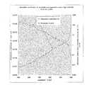
図35は、チャネル層及び光電変換層としてPoly−Siを用いた場合に、光の波長(λ)を横軸、吸収係数(α)を左縦軸、光の強さ1/eになる膜厚を右縦軸にとったグラフである。また、図36は、チャネル層及び光電変換層としてa-Si:Hを用いた場合に、光の波長(λ)を横軸、吸収係数(α)を左縦軸、光の強さ1/eになる膜厚を右縦軸にとったグラフである。 FIG. 35 shows a film in which light wavelength (λ) is plotted on the horizontal axis, absorption coefficient (α) is plotted on the left vertical axis, and light intensity is 1 / e when Poly-Si is used for the channel layer and the photoelectric conversion layer. It is the graph which took thickness on the right vertical axis. FIG. 36 shows the case where a-Si: H is used for the channel layer and the photoelectric conversion layer, the light wavelength (λ) is the horizontal axis, the absorption coefficient (α) is the left vertical axis, and the
図35及び図36から分かるように、光を効率よく吸収するためには、少なくとも100nm以上の膜厚が必要となる。そこで、光センサの感度を上げるために、チャネル層及び光電変換層に相当する部分の膜厚を厚くすると、Poly−SiTFTの場合は、例えばトランジスタのオフ電流が高くなる、光リークが増加する、エキシマレーザ等を用いたレーザーアニール処理による結晶化が困難になる、などの不具合を招く。また、a-Si:HTFTの場合にも、例えばオフ電流が高くなる、S−D抵抗が増える、光リークが増加する、などの不具合を招く。 As can be seen from FIGS. 35 and 36, in order to efficiently absorb light, a film thickness of at least 100 nm is required. Therefore, in order to increase the sensitivity of the photosensor, when the film thickness corresponding to the channel layer and the photoelectric conversion layer is increased, in the case of Poly-Si TFT, for example, the off-current of the transistor is increased, and light leakage is increased. This causes problems such as difficulty in crystallization by laser annealing using an excimer laser or the like. Also in the case of a-Si: HTFT, for example, the off current increases, the SD resistance increases, and the light leakage increases.
本発明は、上記課題を解決するためになされたもので、その目的とするところは、基板の下地層の上にスイッチング素子と光センサ素子を形成する場合に、スイッチング素子とは別個に光センサ素子の感度特性を制御することにより、スイッチング素子の特性に影響を与えることなく、光センサ素子の感度を向上させることができる表示装置及びその製造方法を提供することにある。 The present invention has been made in order to solve the above-described problems, and an object of the present invention is to provide an optical sensor separately from the switching element when the switching element and the optical sensor element are formed on the base layer of the substrate. It is an object of the present invention to provide a display device that can improve the sensitivity of a photosensor element without affecting the characteristics of a switching element by controlling the sensitivity characteristic of the element, and a method for manufacturing the same.
本発明に係る表示装置は、複数の画素がマトリクス状に配置される基板の下地層の上に、前記画素のスイッチング素子を構成する第1の活性層と光センサ素子を構成する第2の活性層とを有し、前記第2の活性層は、前記第1の活性層よりも光吸収率が高いものとなっている。
本発明に係る表示装置の製造方法は、複数の画素をマトリクス状に形成するための基板の下地層の上に、前記画素のスイッチング素子を構成する第1の活性層を形成し、前記1の活性層と同じ前記下地層の上に、光センサ素子を構成する第2の活性層を、前記第1の活性層より光吸収率が高くなるように形成するものである。
また、本発明に係る表示装置の製造方法は、複数の画素をマトリクス状に形成するための基板の下地層の上に、前記画素のスイッチング素子を構成する第1の活性層を形成し、前記1の活性層と同じ前記下地層の上に、光センサ素子を構成する第2の活性層を、前記第1の活性層と異なる層厚または異なる材料により形成するものである。
ここで記述する「光吸収率」とは、活性層に光が入射したときに、当該活性層に吸収される、単位面積あたりの光の割合(入射光量を100%としたときに活性層に吸収される光量の比率)をいう。例えば、単位面積を1平方μmの大きさで規定すると、1平方μmあたり活性層に入射する光量Q1と当該活性層に吸収される光量Q2の割合(Q2÷Q1)が光吸収率となる。The display device according to the present invention includes a first active layer that constitutes a switching element of the pixel and a second active element that constitutes a photosensor element on a base layer of a substrate on which a plurality of pixels are arranged in a matrix. The second active layer has a higher light absorption rate than the first active layer.
In the method for manufacturing a display device according to the present invention, a first active layer constituting a switching element of the pixel is formed on a base layer of a substrate for forming a plurality of pixels in a matrix, On the same base layer as the active layer, a second active layer constituting the photosensor element is formed so that the light absorption rate is higher than that of the first active layer.
In the method for manufacturing a display device according to the present invention, a first active layer constituting a switching element of the pixel is formed on a base layer of a substrate for forming a plurality of pixels in a matrix. On the same base layer as the first active layer, a second active layer constituting the photosensor element is formed with a layer thickness different from that of the first active layer or a different material.
The “light absorptance” described here is the ratio of light per unit area that is absorbed in the active layer when light enters the active layer (when the incident light quantity is 100%, The ratio of the amount of light absorbed). For example, if the unit area is defined by a size of 1 square μm, the ratio (Q2 ÷ Q1) of the amount of light Q1 incident on the active layer and the amount of light Q2 absorbed by the active layer per square μm is the light absorption rate.
本発明に係る表示装置及びその製造方法においては、スイッチング素子を構成する第1の活性層に比較して、光センサ素子を構成する第2の活性層の光吸収率を高くすることにより、スイッチング素子とは別個に光センサ素子の感度特性を制御することが可能となる。このため、スイッチング素子の特性を変えることなく、光センサ素子の感度を高めることが可能となる。
また、本発明に係る表示装置の製造方法においては、スイッチング素子を構成する第1の活性層と異なる層の厚みや材料で第2の活性層を1の活性層と同じ下地層の上に形成することにより、スイッチング素子とは別個に光センサ素子の感度特性を制御することが可能となる。このため、スイッチング素子の特性を変えることなく、光センサ素子の感度を高めることが可能となる。In the display device and the manufacturing method thereof according to the present invention, switching is performed by increasing the light absorptance of the second active layer constituting the photosensor element as compared with the first active layer constituting the switching element. It becomes possible to control the sensitivity characteristic of the optical sensor element separately from the element. For this reason, it is possible to increase the sensitivity of the optical sensor element without changing the characteristics of the switching element.
In the method for manufacturing a display device according to the present invention, the second active layer is formed on the same underlayer as the one active layer with a thickness and material different from those of the first active layer constituting the switching element. By doing so, it becomes possible to control the sensitivity characteristic of the optical sensor element separately from the switching element. For this reason, it is possible to increase the sensitivity of the optical sensor element without changing the characteristics of the switching element.
本発明によれば、光センサ付きの表示装置において、スイッチング素子の特性に影響を与えることなく、光センサ素子の感度を向上させることができる。 According to the present invention, in a display device with an optical sensor, the sensitivity of the optical sensor element can be improved without affecting the characteristics of the switching element.
以下、本発明の具体的な実施の形態について図面を参照しつつ詳細に説明する。 Hereinafter, specific embodiments of the present invention will be described in detail with reference to the drawings.
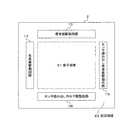
図1(A)は液晶表示装置の構成例を示す平面図であり、図1(B)は同側面図、図1(C)は同要部断面図である。図示した液晶表示装置1は、駆動基板2と対向基板3とを貼り合わせた構造の表示パネルを備えている。表示パネルは、表示領域E1と、当該表示領域E1に隣接する周辺領域E2とに区分されている。周辺領域E2は表示領域E1の周辺に位置している。駆動基板2と対向基板3との間には、図示しないスペーサやシールを用いて液晶層4が封入されている。 FIG. 1A is a plan view illustrating a configuration example of a liquid crystal display device, FIG. 1B is a side view thereof, and FIG. The illustrated liquid
駆動基板2は、透明なガラス基板(絶縁性の基板)5を用いて構成されている。ガラス基板5の一方の面には画素電極6が形成されている。ガラス基板5の他方の面には偏光板7が貼り付けられている。対向基板3は、透明なガラス基板(絶縁性の基板)8を用いて構成されている。ガラス基板8の一方の面には共通電極(対向電極)9が形成されている。ガラス基板8の他方の面には偏光板10が貼り付けられている。駆動基板2と対向基板3は、液晶層4を介して画素電極6と共通電極9を対向させた状態で配置されている。 The
駆動基板2の表示領域E1には、図2に示すように、画像を表示するための複数の画素11がマトリクス状に配置されている。駆動基板2の周辺領域E2には、走査線駆動回路12と信号線駆動回路13が配置されている。走査線駆動回路12は、水平方向に配線された複数の走査線14を選択的に駆動するものである。信号線駆動回路13は、垂直方向に配線された複数の信号線15を選択的に駆動するものである。画素11は、駆動基板2の表示領域E1内で、走査線14と信号線15が交差する部分に1つずつ設けられている。各々の画素11には上記画素電極6を含む画素回路が設けられている。 In the display area E1 of the
画素回路は、例えば画素電極6、薄膜トランジスタTr及び保持容量Csを用いて構成されている。画素電極6は、薄膜トランジスタTrのドレイン電極に接続されている。薄膜トランジスタTrのゲート電極は走査線14に接続されている。薄膜トランジスタTrのソース電極は信号線15に接続されている。 The pixel circuit is configured using, for example, a pixel electrode 6, a thin film transistor Tr, and a storage capacitor Cs. The pixel electrode 6 is connected to the drain electrode of the thin film transistor Tr. The gate electrode of the thin film transistor Tr is connected to the
上記構成の画素回路においては、走査線駆動回路12と信号線駆動回路13の駆動により、薄膜トランジスタTrを介して信号線15から書き込まれた映像信号が保持容量Csに保持されるとともに、そこに保持された信号量に応じた電圧が画素電極6に供給され、この電圧に応じて上記液晶層4を構成する液晶分子が傾斜して表示光の透過が制御される仕組みになっている。 In the pixel circuit having the above configuration, the video signal written from the
なお、上記のような画素回路の構成は、あくまでも一例であり、必要に応じて画素回路内に容量素子を設けたり、さらに複数のトランジスタを設けたりして画素回路を構成してもよい。また、周辺領域E2には、画素回路の変更に応じて必要な駆動回路や素子を追加してもよい。 Note that the configuration of the pixel circuit as described above is merely an example, and the pixel circuit may be configured by providing a capacitive element in the pixel circuit or further providing a plurality of transistors as necessary. Further, necessary drive circuits and elements may be added to the peripheral region E2 in accordance with the change of the pixel circuit.
図3は表示パネルの表示領域における回路構成を示す図である。図示のように、駆動基板2には、画素11とセンサ部100とが設けられている。画素11とセンサ部100は、それぞれ上記表示領域E1に複数設けられるものである。また、複数の画素11は、表示領域E1全体に渡ってマトリクス状に配置され、複数のセンサ部100も、表示領域E1全体に渡ってマトリクス状に配置されるものである。センサ部100は、画素11に対応付けて表示領域E1に設けられている。具体的には、赤(R),緑(G),青(B)の各色成分に対応するサブ画素と1:1の対応関係でセンサ部100を配置する場合が考えられる。また、RGBの3つのサブ画素を一つの組としたメイン画素と1:1の対応関係でセンサ部110を配置する場合も考えられる。また、複数個のメイン画素につき1個のセンサ部100を対応付けて配置する場合も考えられる。また、センサ部100に関しては、表示領域E1の全体ではなく、表示領域E1の一部(所定部位)に限定して設けてもよい。表示領域E1に画素11とセンサ部100の両方を設ける場合、画素11は有効表示部に設け、センサ部100は無効表示部に設けるようにする。有効表示部とは、液晶層4を用いて光の透過を制御することにより、画像の表示に寄与する部分をいう。無効表示部は、表示領域E1内で有効表示部を除く部分をいう。 FIG. 3 is a diagram showing a circuit configuration in the display area of the display panel. As illustrated, the
センサ部100は光センサ素子101を備えている。光センサ素子101は、上記薄膜トランジスタTrと並行した製造工程(詳細は後述)で駆動基板2に形成されるものである。光センサ素子101には、電源電圧VDDが供給されるようになっている。また、光センサ素子101には、リセット用のスイッチング素子102とコンデンサ(蓄積容量)103が接続されている。光センサ素子101は、光の入射(照射)によって電子正孔対を発生することにより、受光量に応じた光電流を生成するものである。この光電流は、光センサ素子101の受光信号としてセンサ外部に読み出される。また、光センサ素子101の受光信号(信号電荷)はコンデンサ103に蓄積される。スイッチング素子102は、コンデンサ103に蓄積された受光信号を所定のタイミングでリセットする。コンデンサ103に蓄積された受光信号は、読み出し用のスイッチング素子104がオンとなるタイミングで、バッファアンプ105を介して受光信号配線106に供給(読み出し)され、外部へ出力される。リセット用のスイッチング素子102のオン・オフ動作は、リセット制御線107により供給されるリセット信号により制御される。また、読み出し用のスイッチング素子104のオン・オフ動作は、読み出し制御線108により供給される読み出し信号により制御される。光センサ素子101の受光信号の読み出しは、例えば図4に示すように、表示パネルを構成する駆動基板2の周辺領域E2に設けられたセンサ読み出し用水平駆動回路109とセンサ読み出し用垂直駆動回路110によって行なわれる。 The
<第1実施形態>
図5は本発明の第1実施形態に係る液晶表示装置1の駆動基板2の主要部を示す断面図である。図示のように、駆動基板2のベースとなるガラス基板5上には、画素11のスイッチング素子(薄膜トランジスタTr)を構成する第1の素子形成部21と、センサ部100の光センサ素子101を構成する第2の素子形成部22が設けられている。上記図1に示す液晶層4側からガラス基板5を平面視すると、第1の素子形成部21は上記画素11とともに表示領域E1に配置され、第2の素子形成部22は、上記センサ部100とともに表示領域E1に配置されている。ただし、これに限らず、第1の素子形成部21は、表示領域E1と周辺領域E2の両方に配置してもよい。また、第2の素子形成部22は、周辺領域E2に配置してもよいし、表示領域E1と周辺領域E2の両方に配置してもよい。図5においては、説明の便宜上、第1の素子形成部21と第2の素子形成部22を隣り合わせに横並びで表示しているが、特に、この並びに限定されるものではない。<First Embodiment>
FIG. 5 is a cross-sectional view showing the main part of the
第1の素子形成部21は、ガラス基板5上に形成されたゲート電極23と、このゲート電極23にゲート絶縁膜24を介して対向するチャネル層25と、このチャネル層25の両側に位置するソース26及びドレイン27とを含むものである。ゲート電極23は、例えばクロム、モリブデン等の高融点金属を用いて形成されるものである。ゲート絶縁膜24は、高い光透過性を有する膜(透明な絶縁膜)であって、例えば、シリコン窒化膜とシリコン酸化膜の2層構造になっている。 The first
チャネル層25は、「第1の活性層」として第1の素子形成部21に設けられたものであり、ゲート絶縁膜24をその下地層として、ゲート絶縁膜24上に積層するように形成されている。チャネル層25は、上述した第1の素子形成部21の配置に対応して、表示領域E及び周辺領域E2のうち、少なくとも表示領域E1に配置されるものである。すなわち、チャネル層25は、表示領域E1のみ、又は表示領域E1と周辺領域E2の両方に配置されるものである。チャネル層25は、トランジスタON時にゲート電極23に面する側でソース26−ドレイン27間にn型のチャネルを形成するものである。チャネル層25は、例えば多結晶シリコンによって形成されている。 The
ソース26及びドレイン27は、n+型不純物の拡散領域となっている。ソース26は高濃度不純物領域26Hと低濃度不純物領域26Lとを有し、ドレイン27も高濃度不純物領域27Hと低濃度不純物領域27Lとを有している。ソース26の低濃度不純物領域26Lはチャネル層25に隣接し、ドレイン27の低濃度不純物領域27Lもチャネル層25に隣接している。このようにチャネル層25の両側に低濃度の不純物拡散領域を設けた構造は、LDD(Lightly Doped Drain)構造と呼ばれている。The
ソース26の高濃度不純物領域26Hはコンタクト用に低抵抗化された領域で、当該高濃度不純物領域26Hにソース電極28が接続されている。同様に、ドレイン27の高濃度不純物領域27Hはコンタクト用に低抵抗化された領域で、当該高濃度不純物領域27Hにドレイン電極29が接続されている。ソース電極28及びドレイン電極29は、それぞれ層間絶縁膜30を貫通する状態で形成されている。層間絶縁膜30は、高い光透過性を有する膜(透明な絶縁膜)であって、例えばシリコン酸化膜によって構成されている。 The high-
第2の素子形成部22は、ガラス基板5上に形成されたゲート電極33と、このゲート電極33に上記ゲート絶縁膜24を介して対向する光電変換層35と、この光電変換層35の両側に位置するソース36及びドレイン37とを含むものである。 The second
光電変換層35は、「第2の活性層」として第2の素子形成部22に設けられたものである。光電変換層35は、上述した第2の素子形成部22の配置に対応して、表示領域E及び周辺領域E2のうち、少なくとも一方の領域に配置されるものである。すなわち、光電変換層35は、表示領域E1のみ、周辺領域E2のみ、又はその両方の領域に配置されるものである。この光電変換層35は、上記チャネル層25と異なる材料でゲート絶縁膜24上に形成されている。具体的には、例えば、非晶質シリコン(a-si)、非晶質ゲルマニウム(a-Ge)、非晶質シリコンゲルマニウム(a-SixGe1)、シリコンとゲルマニウムの積層層、又はそれらの結晶粒径をナノレベルまで微細化(微結晶化)した材料層などによって光電変換層35が形成されている。また、場合によってカーボンを用いて光電変換層35を形成していてもよい。 The
光電変換層35は、ゲート電極33の上方にソース36及びドレイン37の対向部分を一部被覆する状態で形成されている。光電変換層35は、上記チャネル層25よりも厚く形成されている。例えば、チャネル層25の厚さをトランジスタのOFF電流や直列抵抗などの関係で50nm以上、100nm未満の範囲に設定するものとすると、光電変換層35の厚さは、それよりも厚い100nm以上に設定する。 The
ソース36及びドレイン37は、n+型不純物の拡散領域となっている。ソース36にはソース電極38が接続され、ドレイン37にはドレイン電極39が接続されている。ソース電極38及びドレイン電極39は、それぞれ層間絶縁膜30を貫通する状態で形成されている。The
このように光電変換層35をチャネル層25と異なる材料で形成したり、光電変換層35をチャネル層25よりも厚く形成したりすることにより、光電変換層35の光吸収率(特に、可視光や赤外光の吸収率)をチャネル層25の光吸収率よりも高くしている。すなわち、チャネル層25の形成材料よりも光吸収性の高い材料を用いて光電変換層35を形成すれば、光電変換層35の光吸収率がチャネル層25の光吸収率よりも高くなる。また、仮に同じ形成材料であっても、光電変換層35をチャネル層25よりも厚く形成すれば、光電変換層35の光吸収率がチャネル層25の光吸収率よりも高くなる。つまり、光電変換層35をチャネル層25と同じ厚さ又はそれよりも薄く形成した場合は、光電変換層35をチャネル層25と異なる材料(光吸収性の高い材料)で形成することにより、光電変換層35の光吸収率をチャネル層25のそれよりも高くすることができる。また、光電変換層35をチャネル層25と同じ材料で形成した場合は、光電変換層35の厚さをチャネル層25の厚さよりも厚くすることにより、光電変換層35の光吸収率をチャネル層25のそれよりも高くすることができる。さらに、光電変換層35をチャネル層25よりも光吸収性の高い材料で形成し、かつ光電変換層35をチャネル層25よりも厚く形成することにより、チャネル層25に比較して、光電変換層35の光吸収率を、より一層高くすることができる。 Thus, the
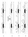
これにより、第2の素子形成部22を光センサ素子として機能させる場合に、光電変換層35への光の入射によって発生する電子−正孔対の数が増加する。このため、第1の素子形成部21と同じ材料及び厚さで光電変換層を形成する場合に比較して、より大きな光電流が得られる。その結果、画素11のスイッチング素子となる薄膜トランジスタTrに影響を与えることなく、光センサ素子の感度を高めることができる。 Thereby, when functioning the 2nd
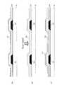
図6及び図7は本発明の第1実施形態に係る液晶表示装置の製造方法を示す図である。まず、図6(A)に示すように、上記複数の画素11をマトリクス状に形成するためのガラス基板5上にゲート電極23,33及びゲート絶縁膜24を形成した後、ゲート絶縁膜24を覆う状態で非晶質シリコンからなる半導体膜31を形成する。ゲート絶縁膜24は、例えばPECVD(plasma enhanced chemical vapor deposition)法などにより、ガラス基板5上にシリコン窒化膜とシリコン酸化膜を順に成膜することで形成する。半導体膜31は、上記第1の素子形成部21と第2の素子形成部22にわたってガラス基板5上に形成する。 6 and 7 are views showing a method of manufacturing the liquid crystal display device according to the first embodiment of the present invention. First, as shown in FIG. 6A, after the
次に、図6(B)に示すように、レーザーアニールによって上記非晶質の半導体膜31を多結晶化することにより、多結晶シリコンからなる半導体膜32を得る。この段階でガラス基板5上に多結晶の半導体膜32が形成された状態となる。 Next, as shown in FIG. 6B, the
次に、図6(C)に示すように、多結晶の半導体膜32に対して、ゲート電極23上でチャネル層25を構成する多結晶シリコン部分を除いた領域に、例えばイオン打ち込み、イオン注入又はプラズマ注入などで不純物を導入することにより、上記半導体膜32を、多結晶シリコン領域32Pと、高濃度不純物領域32Hと、低濃度不純物領域32Lに区分する。 Next, as shown in FIG. 6C, for example, ion implantation or ion implantation is performed on the
次に、図6(D)に示すように、上記第1の素子形成部21と第2の素子形成部22に対応する部分で、ウェットエッチング又はドライエッチングによって半導体膜32を島状に分離することにより、上記第1の素子形成部21に含まれるゲート電極23側にチャネル層25とソース26とドレイン27を形成し、上記第2の素子形成部22に含まれるゲート電極33側にソース36とドレイン37を形成する。このとき、ソース26は高濃度不純物領域26Hと低濃度不純物領域26Lに区分され、ドレイン27も高濃度不純物領域27Hと低濃度不純物領域27Lに区分される。また、ゲート電極33上では、活性層(光電変換層)に相当する部分(トランジスタの構造的にはチャネル層に相当する部分)の半導体膜32を除去することにより、ソース36とドレイン37の間でゲート絶縁膜24の表面を露出させる。 Next, as shown in FIG. 6D, the
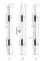
次に、図7(A)に示すように、ゲート電極33上で半導体膜32を除去した部分(活性層相当部)に、例えばインクジェット成膜法等の印刷法、レーザCVD等の光CVD法又はスタンピング法などの選択的膜形成法によって光電変換層35を形成する。インクジェット成膜法や光CVD法では、膜厚を任意に制御することができる。このため、ここでは上記半導体膜32よりも膜厚を厚くして光電変換層35を形成する。 Next, as shown in FIG. 7A, a portion of the
次に、図7(B)に示すように、チャネル層25、ソース26及びドレイン27と、光電変換層35、ソース36及びドレイン37とを覆う状態で、ガラス基板5上に層間絶縁膜30を形成する。 Next, as illustrated in FIG. 7B, the
次に、図7(C)に示すように、チャネル層25の両側でソース26の高濃度不純物領域26Hに通じるコンタクトホールとドレイン27の高濃度不純物領域27Hに通じるコンタクトホールを形成し、これらのコンタクトホールを配線材料で埋め込む状態で層間絶縁膜30にソース電極28とドレイン電極29を形成する。また、これと並行して、光電変換層35の両側でソース36に通じるコンタクトホールとドレイン37に通じるコンタクトホールを形成し、これらのコンタクトホールを配線材料で埋め込む状態でソース電極38とドレイン電極39を形成する。 Next, as shown in FIG. 7C, contact holes that lead to the high-
以上の製造方法により、チャネル層25を含むスイッチング素子(薄膜トランジスタ)と光電変換層35を含む光センサ素子を同一のガラス基板5上に形成することができる。また、第1の素子形成部21で画素のスイッチング素子(薄膜トランジスタ)を構成するチャネル層25と、第2の素子形成部22で光センサ素子を構成する光電変換層35を、それぞれ異なる材料及び厚さで形成することができる。 With the above manufacturing method, the switching element (thin film transistor) including the
ちなみに、スイッチング素子を構成するチャネル層25と光センサ素子を構成する光電変換層35を、それぞれPECVD法やスパッタ法などで別々に成膜した場合は、活性層相当部以外の不要な箇所にも成膜されるため、成膜後にエッチングなどで不要な部分を除去する必要がある。このため、工程が非常に複雑になる。また、エッチングで素子にダメージを与えたり、パーティクルが増えたりする恐れもある。これに対して、上述のように第2の素子形成部22で活性層相当部に選択的膜形成法によって光電変換層35を形成すれば、そうした問題を回避することができる。 By the way, when the
<第2実施形態>
図8は本発明の第2実施形態に係る液晶表示装置1の駆動基板2の主要部を示す断面図である。この第2実施形態においては、上記第1実施形態と比較して、特に、第2の素子形成部22のゲート電極33上に光反射膜40を設けた点が異なる。光反射膜40は、外光が入射する側と反対側で光電変換層35に最も近接して対向配置されるゲート電極33の表面に形成されている。また光反射膜40は、少なくともゲート電極33よりも光の反射率が高い材料、例えば銀などの金属材料を用いて形成されている。Second Embodiment
FIG. 8 is a cross-sectional view showing the main part of the
このようにゲート電極33を覆うように光反射膜40を設けることにより、外部から入射して光電変換層35を透過した光が、光反射膜40で効率良く反射し、この反射光が戻り光となって再び光電変換層35に入射するようになる。このため、外部からの光が光電変換層35に入射する回数が増える。その結果、光電変換層35で発生する電子−正孔対の数が増加し、光センサ素子としての感度が向上する。 By providing the
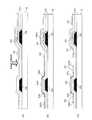
図9〜図11は本発明の第2実施形態に係る液晶表示装置の製造方法を示す図である。まず、図9(A)に示すように、上記複数の画素11をマトリクス状に形成するためのガラス基板5上にゲート電極23,33を形成する。その後、一方のゲート電極33上に、当該ゲート電極33を覆う状態で、例えばインクジェット成膜法により銀を選択的に成膜することにより、光反射膜40を形成する。 9 to 11 are views showing a method of manufacturing a liquid crystal display device according to the second embodiment of the present invention. First, as shown in FIG. 9A,
次に、図9(B)に示すように、ゲート電極23とゲート電極33上の光反射膜40を覆う状態で、例えばPECVD(plasma enhanced chemical vapor deposition)法などにより、ガラス基板5上にシリコン窒化膜とシリコン酸化膜を順に成膜してゲート絶縁膜24を形成する。 Next, as shown in FIG. 9B, in a state where the
次に、図9(C)に示すように、PECVD法などにより、ゲート絶縁膜24を覆う状態で非晶質シリコンからなる半導体膜31を形成する。半導体膜31は、上記第1の素子形成部21と第2の素子形成部22にわたってガラス基板5上に形成する。 Next, as shown in FIG. 9C, a
次に、図10(A)に示すように、レーザーアニールによって上記非晶質の半導体膜31を多結晶化することにより、多結晶シリコンからなる半導体膜32を得る。この段階でガラス基板5上に多結晶の半導体膜32が形成された状態となる。 Next, as shown in FIG. 10A, the
次に、図10(B)に示すように、多結晶の半導体膜32に対して、ゲート電極23上でチャネル層25を構成する多結晶シリコン部分を除いた領域に、例えばイオン打ち込み、イオン注入又はプラズマ注入などで不純物を導入することにより、上記半導体膜32を、多結晶シリコン領域32Pと、高濃度不純物領域32Hと、低濃度不純物領域32Lに区分する。このとき、イオン注入等を行なう前に、半導体層32を保護する目的で酸化物などをスパッタ法で形成してもよい。 Next, as shown in FIG. 10B, for example, ion implantation and ion implantation are performed on the
次に、図10(C)に示すように、上記第1の素子形成部21と第2の素子形成部22に対応する部分で、ウェットエッチング又はドライエッチングによって半導体膜32を島状に分離することにより、上記第1の素子形成部21に含まれるゲート電極23側にソース26とドレイン27を形成し、上記第2の素子形成部22に含まれるゲート電極33側にソース36とドレイン37を形成する。このとき、ソース26は高濃度不純物領域26Hと低濃度不純物領域26Lに区分され、ドレイン27も高濃度不純物領域27Hと低濃度不純物領域27Lに区分される。また、ゲート電極33(光反射膜40)上では、活性層(光電変換層)に相当する部分の半導体膜32を除去することにより、ソース36とドレイン37の間でゲート絶縁膜24を露出させる。 Next, as shown in FIG. 10C, the
次に、図11(A)に示すように、ゲート電極33(光反射膜40)上で半導体膜32を除去した部分に、例えばインクジェット成膜法等の印刷法、レーザCVD等の光CVD法又はスタンピング法などの選択的膜形成法によって光電変換層35を形成する。インクジェット成膜法や光CVD法では、膜厚を任意に制御することができる。このため、ここでは上記半導体膜32よりも膜厚を厚くして光電変換層35を形成する。 Next, as shown in FIG. 11A, a portion of the gate electrode 33 (light reflecting film 40) from which the
次に、図11(B)に示すように、チャネル層25、ソース26及びドレイン27と、光電変換層35、ソース36及びドレイン37とを覆う状態で、ガラス基板5上に層間絶縁膜30を形成する。 Next, as illustrated in FIG. 11B, the
次に、図11(C)に示すように、チャネル層25の両側でソース26の高濃度不純物領域26Hに通じるコンタクトホールとドレイン27の高濃度不純物領域27Hに通じるコンタクトホールを形成し、これらのコンタクトホールを配線材料で埋め込む状態で層間絶縁膜30にソース電極28とドレイン電極29を形成する。また、それと並行して、光電変換層35の両側でソース36に通じるコンタクトホールとドレイン37に通じるコンタクトホールを形成し、これらのコンタクトホールを配線材料で埋め込む状態でソース電極38とドレイン電極39を形成する。 Next, as shown in FIG. 11C, contact holes that lead to the high-
以上の製造方法により、チャネル層25を含むスイッチング素子(薄膜トランジスタ)と光電変換層35を含む光センサ素子を同一のガラス基板5上に形成することができる。また、第1の素子形成部21で画素のスイッチング素子(薄膜トランジスタ)を構成するチャネル層25と、第2の素子形成部22で光センサ素子を構成する光電変換層35を、それぞれ異なる材料及び厚さで形成することができる。さらに、第2の素子形成部22では、ゲート電極33上に光反射膜40を設けることができる。 With the above manufacturing method, the switching element (thin film transistor) including the
<第3実施形態>
図12は本発明の第3実施形態に係る液晶表示装置1の駆動基板2の主要部を示す断面図である。この第3実施形態においては、上記第1実施形態と比較して、特に、透明LCD(Liquid Crystal Display)を実現するために、第1の素子形成部21のゲート電極23を透明電極とした点と、ソース26,36及びドレイン27,37をそれぞれ透明導電膜で形成した点と、ソース電極28,38及びドレイン電極29,39をそれぞれ透明電極とした点と、チャネル層25を透明な半導体膜で形成した点と、ゲート電極33を金属遮蔽電極とした点と、第2の素子形成部22を周辺領域E2だけに配置する点が異なる。<Third Embodiment>
FIG. 12 is a cross-sectional view showing the main part of the
ゲート電極23は、例えばITOなどの透明導電材料を用いて形成されている。ソース26,36及びドレイン27,37の各々は、例えばITO(Indium Tin Oxide)、ZnO(酸化亜鉛)、FZO(フッ素含有ZnO)、GZO(ガリウム含有ZnO)、FGZO(フッ素・ガリウム含有ZnO)、AZO(アルミニウム含有ZnO)などの透明導電材料を用いて形成されている。 The
ソース電極28,38及びドレイン電極29,39の各々は、例えばTI/Al/TIを用いて形成されている。チャネル層25は、例えばInGaZnO及びIZOを用いて形成されている。ゲート電極33は、例えば銀を用いて形成されている。 Each of the
このように第3実施形態に係る液晶表示装置1では、第1の素子形成部21のチャネル層25を透明な酸化物半導体で形成する一方、第2の素子形成部22の光電変換層35をそれよりも光吸収性の高い材料(非晶質シリコン等)で厚く形成することにより、光電変換層35の光吸収率(特に、可視光や赤外光の吸収率)をチャネル層25の光吸収率よりも高くしている。 Thus, in the liquid
これにより、第2の素子形成部22を光センサ素子として機能させる場合に、光電変換層35への光の入射によって発生する電子−正孔対の数が増加する。このため、第1の素子形成部21と同じ材料及び厚さで光電変換層を形成する場合に比較して、より大きな光電流が得られる。その結果、画素11のスイッチング素子となる薄膜トランジスタTrに影響を与えることなく、光センサ素子の感度を高めることができる。 Thereby, when functioning the 2nd
また、ゲート電極33を金属遮蔽電極で形成しているため、図示しないバックライトから入射する光(以下、「バックライト光」と記す)がゲート電極33によって遮蔽される。このため、光電変換層35に対するバックライト光の入射をゲート電極33で防止することができる。また、ゲート電極33を形成する銀は、高い光反射率を有するため、外部から入射して光電変換層35を透過した光がゲート電極33で反射し、この反射光が戻り光となって再び光電変換層35に入射するようになる。このため、上記第2実施形態と同様の原理で、光センサ素子としての感度が向上する。 Further, since the
また、第3実施形態に係る液晶表示装置1においては、表示領域E1に配置される第1の素子形成部21全体が光を透過するようになるため、非駆動時には表示領域E1を透明な状態とし、駆動時には表示領域E1に画像を表示させることができる。また、第2の素子形成部22のゲート電極33は光を遮蔽し、光電変換層35は光の一部を吸収するものの、表示パネルの面内で第2の素子形成部22を周辺領域E2の目立たない端の位置(例えば、表示パネルの四隅)に配置すれば、表示パネルの透明性を損なうことがない。 Further, in the liquid
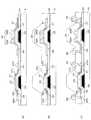
図13及び図14は本発明の第3実施形態に係る液晶表示装置の製造方法を示す図である。まず、図13(A)に示すように、上記複数の画素11をマトリクス状に形成するためのガラス基板5上に透明なゲート電極23を形成する。 13 and 14 are views showing a method of manufacturing a liquid crystal display device according to the third embodiment of the present invention. First, as shown in FIG. 13A, a
次に、図13(B)に示すように、ガラス基板5上に遮光性を有するゲート電極33を形成する。このゲート電極33は、例えば銀を成膜材料としたインクジェット成膜法により形成する。 Next, as shown in FIG. 13B, a light-shielding
次に、図13(C)に示すように、ゲート電極23,33を覆う状態で、例えばPECVD法、スパッタ法、塗布法などにより、ガラス基板5上にシリコン窒化膜とシリコン酸化膜とを順に成膜してゲート絶縁膜24を形成する。 Next, as shown in FIG. 13C, in a state where the
次に、図13(D)に示すように、ゲート絶縁膜24を覆う状態で、スパッタ法や塗布法などにより、ガラス基板5上に透明導電膜41を形成する。透明導電膜41は、上記第1の素子形成部21と第2の素子形成部22にわたってガラス基板5上に形成する。 Next, as illustrated in FIG. 13D, a transparent
次に、図13(E)に示すように、上記第1の素子形成部21と第2の素子形成部22に対応する部分で、ウェットエッチング又はドライエッチングによって透明導電膜41を島状に分離することにより、上記第1の素子形成部21に含まれるゲート電極23側にソース26とドレイン27を形成するとともに、上記第2の素子形成部22に含まれるゲート電極33側にソース36とドレイン37を形成する。また、ゲート電極23上では、活性層(チャネル層)に相当する部分の透明導電膜41を除去することにより、ソース26とドレイン27の間でゲート絶縁膜24の表面を露出させ、ゲート電極33上では、活性層(光電変換層)に相当する部分の透明導電膜41を除去することにより、ソース36とドレイン37の間でゲート絶縁膜24の表面を露出させる。 Next, as shown in FIG. 13E, the transparent
次に、図14(A)に示すように、ゲート電極23上で透明導電膜41を除去した部分に、例えばPECVD法、スパッタ法、蒸着法又は塗布法などで透明な半導体膜からなるチャネル層25を形成する。透明な半導体膜は、例えば透明酸化物半導体又は有機物半導体によって形成する。また、その前に又はその後に、ゲート電極33上で透明導電膜41を除去した部分に、例えばインクジェット成膜法等の印刷法、レーザCVD等の光CVD法又はスタンピング法などの選択的膜形成法によって光電変換層35を形成する。光電変換層35は、光の吸収作用を得るために非透明な半導体膜(例えば、シリコン膜)によって形成する。インクジェット成膜法や光CVD法では、膜厚を任意に制御することができる。このため、ここではチャネル層25よりも膜厚を厚くして光電変換層35を形成する。 Next, as shown in FIG. 14A, a channel layer made of a transparent semiconductor film, for example, by a PECVD method, a sputtering method, a vapor deposition method, a coating method, or the like on the portion where the transparent
次に、図14(B)に示すように、チャネル層25、ソース26及びドレイン27と、光電変換層35、ソース36及びドレイン37とを覆う状態で、ガラス基板5上に層間絶縁膜30を形成する。 Next, as illustrated in FIG. 14B, the
次に、図14(C)に示すように、チャネル層25の両側でソース26に通じるコンタクトホールとドレイン27に通じるコンタクトホールを形成し、これらのコンタクトホールを配線材料で埋め込む状態で層間絶縁膜30にソース電極28とドレイン電極29を形成する。また、それと並行して、光電変換層35の両側でソース36に通じるコンタクトホールとドレイン37に通じるコンタクトホールを形成し、これらのコンタクトホールを配線材料で埋め込む状態でソース電極38とドレイン電極39を形成する。 Next, as shown in FIG. 14C, a contact hole leading to the
以上の製造方法により、チャネル層25を含むスイッチング素子(薄膜トランジスタ)と光電変換層35を含む光センサ素子を同一のガラス基板5上に形成することができる。また、第1の素子形成部21で画素のスイッチング素子(薄膜トランジスタ)を構成するチャネル層25と、第2の素子形成部22で光センサ素子を構成する光電変換層35を、それぞれ異なる材料及び厚さで形成することができる。 With the above manufacturing method, the switching element (thin film transistor) including the
このため、光電変換層35の形成材料を任意に選ぶことができる。また、画素のスイッチング素子を構成するチャネル層25は、光を透過する、透明な半導体膜で形成し、光センサ素子を構成する光電変換層35は、光を吸収する、非透明な半導体膜で形成することができる。さらに、第2の素子形成部22では、バックライトからの光が光電変換層35に入射しないように遮蔽する機能と、外部からの光を光電変換層35に戻すように反射させる機能とを兼ね備えるゲート電極33を形成することができる。 For this reason, the formation material of the photoelectric converting
<第4実施形態>
図15は本発明の第4実施形態に係る液晶表示装置1の駆動基板2の主要部を示す断面図である。この第4実施形態においては、上記第1実施形態と比較して、特に、第2の素子形成部22の構成が異なる。すなわち、第2の素子形成部22において、光電変換層35は、第1層35Aとその上に積層された第2層35Bとを含む2層の積層構造になっている。第1層35A及び第2層35Bは、それぞれ同一の元素(本形態例ではシリコン)を用いて形成されている。ここでは一例として、光電変換層35を2層の積層構造としているが、これに限らず、3層以上の積層構造で光電変換層35を形成してもよい。光電変換層35の積層数は、成膜工程の工程数によって規定されるものとする。このため、例えば、2回の成膜工程によって光電変換層35を形成した場合は、光電変換層35の積層数が2層となる。第1の素子形成部21には、チャネル層23とソース/ドレイン26,27を覆う状態でマスク層51が形成され、第2の素子形成部22には、ソース/ドレイン36,37を覆う状態でマスク層51が形成されている。マスク層51は、後述する製造方法で光電変換層35を積層構造とするために形成されるものである。さらに、第2の素子形成部22において、ソース36は、高濃度不純物領域36Hと低濃度不純物領域36Lとを有するLDD構造になっており、ドレイン37は、p+型不純物の拡散領域となっている。<Fourth embodiment>
FIG. 15 is a cross-sectional view showing the main part of the
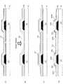
図16〜図18は本発明の第4実施形態に係る液晶表示装置の製造方法を示す図である。まず、図16(A)に示すように、上記複数の画素11をマトリクス状に形成するためのガラス基板5上にゲート電極23,33及びゲート絶縁膜24を形成した後、ゲート絶縁膜24を覆う状態で非晶質シリコンからなる半導体膜31を形成する。ゲート絶縁膜24は、例えばPECVD(plasma enhanced chemical vapor deposition)法などにより、ガラス基板5上にシリコン窒化膜とシリコン酸化膜を順に成膜することで形成する。半導体膜31は、「第1半導体膜」に相当するもので、上記第1の素子形成部21と第2の素子形成部22にわたってガラス基板5上に形成する。 16 to 18 are views showing a method of manufacturing a liquid crystal display device according to the fourth embodiment of the present invention. First, as shown in FIG. 16A, after forming the
次に、図16(B)に示すように、レーザーアニールによって上記非晶質の半導体膜31を多結晶化することにより、多結晶シリコンからなる半導体膜32を得る。この段階でガラス基板5上に多結晶の半導体膜32が形成された状態となる。 Next, as shown in FIG. 16B, the
次に、図16(C)に示すように、ガラス基板5上に半導体膜32を覆う状態でマスク層51を形成する。マスク層51は、例えばシリコン酸化膜によって形成する。このマスク層51により後工程におけるフォトレジストや水などから半導体層を保護すると共に、イオンの加速電圧を制御することでマスク層51を介してイオン注入することができる。 Next, as shown in FIG. 16C, a
次に、図17(A)に示すように、多結晶の半導体膜32に対して、ゲート電極23上でチャネル層25を構成する多結晶シリコン部分とゲート電極33上で光電変換層35を構成する多結晶シリコン部分を除いた領域に、それぞれ不純物を導入する。不純物の導入は、例えばイオン打ち込み、イオン注入又はプラズマ注入などで行なう。これにより、第1の素子形成部21において、上記半導体膜32を、多結晶シリコン領域32Pと、n+型の高濃度不純物領域32Hと、n+型の低濃度不純物領域32Lに区分する。また、第2の素子形成部22において、上記半導体膜32を、多結晶シリコン領域32Pと、n+型の高濃度不純物領域32Hと、n+型の低濃度不純物領域32Lと、p+型の高濃度不純物領域32Mに区分する。Next, as shown in FIG. 17A, with respect to the
次に、図17(B)に示すように、第2の素子形成部22において、マスク層51を部分的に除去することにより、多結晶シリコン領域32Pの表面(上面)を露出させる。マスク層51の除去は、例えばエッチングによって行なう。 Next, as shown in FIG. 17B, in the second
次に、図17(C)に示すように、第2の素子形成部2において、マスク層51を除去した部分に、多結晶シリコン領域32Pと同一の元素(本形態例ではシリコン)を用いて半導体膜52を形成する。半導体膜52は、「第2半導体膜」に相当するもので、例えば、多結晶シリコン、非晶質シリコン、結晶粒子径がナノオーダーのナノ−シリコン、結晶粒子径がミクロンオーダーのμ−シリコンなどによって形成される。半導体膜52の形成は、例えば、熱CVD法、反応性熱CVD法、PECVD法、反応性PECVD法、スパッタ法、光CVD法、PLD(pulse laser deposition)法、溶剤印刷法などで行なう。この場合、半導体膜52となるシリコン膜は、マスク層51を除去した部分で露出している多結晶シリコン領域32Pの表面で選択的に成長する。このため、シリコンによって形成されている多結晶シリコン領域32Pの上に、それと同じシリコンによって半導体膜52が形成されることになる。したがって、多結晶シリコン領域32Pを構成している下地の多結晶シリコンが核になって、半導体膜52を構成するシリコン膜が成長する。このため、核となる多結晶シリコンがないまま、シリコン膜を熱CVD法等により形成する場合に比較して、膜の成長速度を速めることができる。また、プロセス条件等を適宜制御することにより、レーザーアニール等を行なわなくても、結晶性を有する良質のシリコン膜(マイクロクリスタルシリコン膜)を形成することが可能となる。 Next, as shown in FIG. 17C, in the second
なお、半導体膜52を形成する前に、結晶を高めるために、酸化処理によって多結晶シリコン領域32P表面の自然酸化膜を除去した後、ニッケル、金などのcatalystsを、光が透過する程度に薄く成膜してもよい。 Before the
次に、図18(A)に示すように、上記第1の素子形成部21と第2の素子形成部22に対応する部分で、ウェットエッチング又はドライエッチングによって半導体膜32とこれを覆うマスク層51を島状に分離する。これにより、上記第1の素子形成部21にチャネル層25を形成し、上記第2の素子形成部22に光電変換層35を形成する。また、上記第1の素子形成部21に含まれるゲート電極23側にソース26とドレイン27を形成し、上記第2の素子形成部22に含まれるゲート電極33側にソース36とドレイン37を形成する。このとき、第1の素子形成部21において、多結晶シリコン領域32Pはチャネル層25となり、第2の素子形成部22において、多結晶シリコン領域32Pと半導体膜52はそれぞれ第1層35Aと第2層35Bとなり、それらの積層部分が光電変換層35となる。また、第1の素子形成部21において、ソース26は、n+型の高濃度不純物領域26Hと低濃度不純物領域26Lに区分され、ドレイン27も、n+型の高濃度不純物領域27Hと低濃度不純物領域27Lに区分される。また、第2の素子形成部22において、ソース36は、n+型の高濃度不純物領域36Hと低濃度不純物領域36Lに区分され、ドレイ37は、p+型の高濃度不純物領域となる。Next, as shown in FIG. 18A, the
次に、図18(B)に示すように、チャネル層25、ソース26及びドレイン27と、光電変換層35、ソース36及びドレイン37とを覆う状態で、ガラス基板5上に層間絶縁膜30を形成する。 Next, as illustrated in FIG. 18B, the
次に、図18(C)に示すように、チャネル層25の両側でソース26の高濃度不純物領域26Hに通じるコンタクトホールとドレイン27の高濃度不純物領域27Hに通じるコンタクトホールを形成する。そして、これらのコンタクトホールを配線材料で埋め込む状態で層間絶縁膜30にソース電極28とドレイン電極29を形成する。また、それと並行して、光電変換層35の両側でソース36の高濃度不純物領域36Hに通じるコンタクトホールとドレイン37に通じるコンタクトホールを形成する。そして、これらのコンタクトホールを配線材料で埋め込む状態でソース電極38とドレイン電極39を形成する。 Next, as shown in FIG. 18C, a contact hole leading to the high
以上の製造方法により、チャネル層25を含むスイッチング素子(薄膜トランジスタ)と光電変換層35を含む光センサ素子を同一のガラス基板5上に形成することができる。また、光センサ素子の光電変換層35を、それぞれ同一元素となるシリコンを含む第1層35Aと第2層35Bの積層構造で形成することができる。また、光電変換層35の第1層35Aは、チャネル層25と同一工程で形成される層、つまりチャネル層25と同じ厚さの層となる。このため、第1層35Aの上に第2層35Bを積層することで、光電変換層35をチャネル層25よりも厚く形成することができる。 With the above manufacturing method, the switching element (thin film transistor) including the
なお、上記第4実施形態においては、第2の素子形成部22でソース36をLDD構造とし、ドレイン37をp+型の高濃度不純物領域としたが、これに限らず、ソース36をp+型の高濃度不純物領域とし、ドレイン37をLDD構造としてもよい。In the fourth embodiment, the
<第5実施形態>
図19は本発明の第5実施形態に係る液晶表示装置1の駆動基板2の主要部を示す断面図である。この第5実施形態においては、上記第4実施形態と比較して、特に、第2の素子形成部22のソース36が、LDD構造ではなく、p+型不純物の拡散領域となっている点が異なる。<Fifth Embodiment>
FIG. 19 is a cross-sectional view showing the main part of the
図20〜図22は本発明の第5実施形態に係る液晶表示装置の製造方法を示す図である。まず、図20(A)に示すように、上記複数の画素11をマトリクス状に形成するためのガラス基板5上にゲート電極23,33及びゲート絶縁膜24を形成した後、ゲート絶縁膜24を覆う状態で非晶質シリコンからなる半導体膜31を形成する。半導体膜31は、上記第1の素子形成部21と第2の素子形成部22にわたってガラス基板5上に形成する。 20 to 22 are views showing a method of manufacturing a liquid crystal display device according to the fifth embodiment of the present invention. First, as shown in FIG. 20A, after the
次に、図20(B)に示すように、レーザーアニールによって上記非晶質の半導体膜31を多結晶化することにより、多結晶シリコンからなる半導体膜32を得る。 Next, as shown in FIG. 20B, the
次に、図20(C)に示すように、ガラス基板5上に半導体膜32を覆う状態でマスク層51を形成する。ここまでの工程は、上記4実施形態の場合と同様である。 Next, as shown in FIG. 20C, a
次に、図21(A)に示すように、多結晶の半導体膜32に対して、ゲート電極23上でチャネル層25を構成する多結晶シリコン部分とゲート電極33上で光電変換層35を構成する多結晶シリコン部分を除いた領域に、それぞれ不純物を導入する。不純物の導入は、例えばイオン打ち込み、イオン注入又はプラズマ注入などで行なう。これにより、第1の素子形成部21において、上記半導体膜32を、多結晶シリコン領域32Pと、n+型の高濃度不純物領域32Hと、n+型の低濃度不純物領域32Lに区分する。また、第2の素子形成部22において、上記半導体膜32を、多結晶シリコン領域32Pと、n+型の高濃度不純物領域32H、p+型の高濃度不純物領域32Mに区分する。Next, as shown in FIG. 21A, a
次に、図21(B)に示すように、第2の素子形成部22において、マスク層51を部分的に除去することにより、多結晶シリコン領域32Pの表面(上面)を露出させる。 Next, as shown in FIG. 21B, in the second
次に、図21(C)に示すように、第2の素子形成部2において、マスク層51を除去した部分に、多結晶シリコン領域32Pと同一の元素(本形態例ではシリコン)を用いて半導体膜52を形成する。半導体膜52の形成手法に関しては、上記第4実施形態の場合と同様である。 Next, as shown in FIG. 21C, in the second
次に、図22(A)に示すように、上記第1の素子形成部21と第2の素子形成部22に対応する部分で、ウェットエッチング又はドライエッチングによって半導体膜32とこれを覆うマスク層51を島状に分離する。これにより、上記第1の素子形成部21にチャネル層25を形成し、上記第2の素子形成部22に光電変換層35を形成する。また、上記第1の素子形成部21に含まれるゲート電極23側にソース26とドレイン27を形成し、上記第2の素子形成部22に含まれるゲート電極33側にソース36とドレイン37を形成する。このとき、第1の素子形成部21において、多結晶シリコン領域32Pはチャネル層25となり、第2の素子形成部22において、多結晶シリコン領域32Pと半導体膜52はそれぞれ第1層35Aと第2層35Bとなり、それらの積層部分が光電変換層35となる。また、第1の素子形成部21において、ソース26は、n+型の高濃度不純物領域26Hと低濃度不純物領域26Lに区分され、ドレイン27も、n+型の高濃度不純物領域27Hと低濃度不純物領域27Lに区分される。また、第2の素子形成部22において、ソース36は、n+型の高濃度不純物領域となり、ドレイ37は、p+型の高度不純物領域となる。Next, as shown in FIG. 22A, a
次に、図22(B)に示すように、チャネル層25、ソース26及びドレイン27と、光電変換層35、ソース36及びドレイン37とを覆う状態で、ガラス基板5上に層間絶縁膜30を形成する。 Next, as illustrated in FIG. 22B, the
次に、図22(C)に示すように、チャネル層25の両側でソース26の高濃度不純物領域26Hに通じるコンタクトホールとドレイン27の高濃度不純物領域27Hに通じるコンタクトホールを形成する。そして、これらのコンタクトホールを配線材料で埋め込む状態で層間絶縁膜30にソース電極28とドレイン電極29を形成する。また、それと並行して、光電変換層35の両側でソース36に通じるコンタクトホールとドレイン37に通じるコンタクトホールを形成する。そして、これらのコンタクトホールを配線材料で埋め込む状態でソース電極38とドレイン電極39を形成する。 Next, as shown in FIG. 22C, contact holes that lead to the high-
以上の製造方法により、上記図19に示す構成の駆動基板2が得られる。なお、第5実施形態においては、第2の素子形成部22でソース36をn+型の高濃度不純物領域とし、ドレイン37をp+型の高濃度不純物領域としたが、これに限らない。すなわち、ソース36をp+型の高濃度不純物領域とし、ドレイン37をn+型の高濃度不純物領域としてもよい。With the above manufacturing method, the
<第6実施形態>
図23は本発明の第6実施形態に係る液晶表示装置1の駆動基板2の主要部を示す断面図である。この第6実施形態においては、上記第5実施形態と比較して、特に、第2の素子形成部22のソース/ドレイン36,37が、共にn+型不純物の拡散領域となっている点が異なる。<Sixth Embodiment>
FIG. 23 is a cross-sectional view showing the main part of the
図24〜図25は本発明の第1実施形態に係る液晶表示装置の製造方法を示す図である。まず、図24(A)に示すように、上記複数の画素11をマトリクス状に形成するためのガラス基板5上にゲート電極23,33及びゲート絶縁膜24を形成した後、ゲート絶縁膜24を覆う状態で非晶質シリコンからなる半導体膜31を形成する。半導体膜31は、上記第1の素子形成部21と第2の素子形成部22にわたってガラス基板5上に形成する。 24 to 25 are views showing a method of manufacturing the liquid crystal display device according to the first embodiment of the present invention. First, as shown in FIG. 24A, after forming the
次に、図24(B)に示すように、レーザーアニールによって上記非晶質の半導体膜31を多結晶化することにより、多結晶シリコンからなる半導体膜32を得る。 Next, as shown in FIG. 24B, the
次に、図24(C)に示すように、ガラス基板5上に半導体膜32を覆う状態でマスク層52を形成する。ここまでの工程は、上記4実施形態の場合と同様である。 Next, as shown in FIG. 24C, a
次に、図25(A)に示すように、多結晶の半導体膜32に対して、ゲート電極23上でチャネル層25を構成する多結晶シリコン部分とゲート電極33上で光電変換層35を構成する多結晶シリコン部分を除いた領域に、それぞれ不純物を導入する。不純物の導入は、例えばイオン打ち込み、イオン注入又はプラズマ注入などで行なう。これにより、第1の素子形成部21において、上記半導体膜32を、多結晶シリコン領域32Pと、n+型の高濃度不純物領域32Hと、n+型の低濃度不純物領域32Lに区分する。また、第2の素子形成部22において、上記半導体膜32を、多結晶シリコン領域32Pと、n+型の高濃度不純物領域32Hに区分する。Next, as shown in FIG. 25A, a
次に、図25(B)に示すように、第2の素子形成部22において、マスク層51を部分的に除去することにより、多結晶シリコン領域32Pの表面(上面)を露出させる。 Next, as shown in FIG. 25B, in the second
次に、図25(C)に示すように、第2の素子形成部2において、マスク層51を除去した部分に、多結晶シリコン領域32Pと同一の元素(本形態例ではシリコン元素)を用いて半導体膜52を形成する。半導体膜52の形成手法に関しては、上記第4実施形態の場合と同様である。 Next, as shown in FIG. 25C, in the second
次に、図26(A)に示すように、上記第1の素子形成部21と第2の素子形成部22に対応する部分で、ウェットエッチング又はドライエッチングによって半導体膜32とこれを覆うマスク層51を島状に分離する。これにより、上記第1の素子形成部21にチャネル層25を形成し、上記第2の素子形成部22に光電変換層35を形成する。また、上記第1の素子形成部21に含まれるゲート電極23側にソース26とドレイン27を形成し、上記第2の素子形成部22に含まれるゲート電極33側にソース36とドレイン37を形成する。このとき、第1の素子形成部21において、多結晶シリコン領域32Pはチャネル層25となり、第2の素子形成部22において、多結晶シリコン領域32Pと半導体膜52はそれぞれ第1層35Aと第2層35Bとなり、それらの積層部分が光電変換層35となる。また、第1の素子形成部21において、ソース26は、n+型の高濃度不純物領域26Hと低濃度不純物領域26Lに区分され、ドレイン27も、n+型の高濃度不純物領域27Hと低濃度不純物領域27Lに区分される。また、第2の素子形成部22において、ソース36は、n+型の高濃度不純物領域となり、ドレイ37も、n+型の高度不純物領域となる。Next, as shown in FIG. 26A, a
次に、図26(B)に示すように、チャネル層25、ソース26及びドレイン27と、光電変換層35、ソース36及びドレイン37とを覆う状態で、ガラス基板5上に層間絶縁膜30を形成する。 Next, as illustrated in FIG. 26B, the
次に、図26(C)に示すように、チャネル層25の両側でソース26の高濃度不純物領域26Hに通じるコンタクトホールとドレイン27の高濃度不純物領域27Hに通じるコンタクトホールを形成する。そして、これらのコンタクトホールを配線材料で埋め込む状態で層間絶縁膜30にソース電極28とドレイン電極29を形成する。また、それと並行して、光電変換層35の両側でソース36に通じるコンタクトホールとドレイン37に通じるコンタクトホールを形成する。そして、これらのコンタクトホールを配線材料で埋め込む状態でソース電極38とドレイン電極39を形成する。 Next, as shown in FIG. 26C, a contact hole leading to the high
以上の製造方法により、上記図23に示す構成の駆動基板2が得られる。なお、第6実施形態においては、第2の素子形成部22でソース/ドレイン36,37を共にn+型の高濃度不純物領域としたが、これに限らず、ソース/ドレイン36,37を共にp+型の高濃度不純物領域としてもよい。With the above manufacturing method, the
<第7実施形態>
本発明の第7実施形態においては、上記第4実施形態と比較して、特に、液晶表示装置の製造方法が異なる。<Seventh embodiment>
In the seventh embodiment of the present invention, the manufacturing method of the liquid crystal display device is particularly different from that of the fourth embodiment.
図27〜図29は本発明の第7実施形態に係る液晶表示装置の製造方法を示す図である。まず、図27(A)に示すように、上記複数の画素11をマトリクス状に形成するためのガラス基板5上にゲート電極23,33及びゲート絶縁膜24を形成した後、ゲート絶縁膜24を覆う状態で非晶質シリコンからなる半導体膜31を形成する。半導体膜31は、上記第1の素子形成部21と第2の素子形成部22にわたってガラス基板5上に形成する。 27 to 29 are views showing a method of manufacturing a liquid crystal display device according to the seventh embodiment of the present invention. First, as shown in FIG. 27A, after forming the
次に、図27(B)に示すように、レーザーアニールによって上記非晶質の半導体膜31を多結晶化することにより、多結晶シリコンからなる半導体膜32を得る。 Next, as shown in FIG. 27B, the
次に、図27(C)に示すように、ガラス基板5上に半導体膜32を覆う状態でマスク層51を形成する。ここまでの工程は、上記第4実施形態の場合と同様である。 Next, as shown in FIG. 27C, a
次に、図27(D)に示すように、多結晶の半導体膜32に対して、ゲート電極23上でチャネル層25を構成する多結晶シリコン部分とゲート電極33上で光電変換層35を構成する多結晶シリコン部分を除いた領域に、それぞれ不純物を導入する。不純物の導入は、例えばイオン打ち込み、イオン注入又はプラズマ注入などで行なう。これにより、第1の素子形成部21において、上記半導体膜32を、多結晶シリコン領域32Pと、n+型の高濃度不純物領域32Hと、n+型の低濃度不純物領域32Lに区分する。また、第2の素子形成部22において、上記半導体膜32を、多結晶シリコン領域32Pと、n+型の高濃度不純物領域32H、p+型の高濃度不純物領域32Mに区分する。Next, as shown in FIG. 27D, a
次に、図28(A)に示すように、第2の素子形成部22において、マスク層51を部分的に除去することにより、多結晶シリコン領域32Pの表面(上面)を露出させる。 Next, as shown in FIG. 28A, in the second
次に、図28(B)に示すように、第2の素子形成部2において、マスク層51を除去した部分を含めて、ガラス基板5上に、多結晶シリコン領域32Pと同一の元素(本形態例ではシリコン元素)を用いて半導体膜52を形成する。半導体膜52の形成は、例えば、反応CVD法、プラズマCVD法、または熱CVD法などで行なう。 Next, as shown in FIG. 28 (B), in the second
次に、図28(C)に示すように、第2の素子形成部2において、マスク層51を除去した部分だけに半導体膜52が残るように、マスク層51を覆っている半導体膜52をエッチングによって除去する。このとき、マスク層51は、エッチングストッパーとして機能する。 Next, as shown in FIG. 28C, in the second
次に、図29(A)に示すように、上記第1の素子形成部21と第2の素子形成部22に対応する部分で、ウェットエッチング又はドライエッチングによって半導体膜32とこれを覆うマスク層51を島状に分離する。これにより、上記第1の素子形成部21にチャネル層25を形成し、上記第2の素子形成部22に光電変換層35を形成する。また、上記第1の素子形成部21に含まれるゲート電極23側にソース26とドレイン27を形成し、上記第2の素子形成部22に含まれるゲート電極33側にソース36とドレイン37を形成する。このとき、第1の素子形成部21において、多結晶シリコン領域32Pはチャネル層25となり、第2の素子形成部22において、多結晶シリコン領域32Pと半導体膜52はそれぞれ第1層35Aと第2層35Bとなり、それらの積層部分が光電変換層35となる。また、第1の素子形成部21において、ソース26は、n+型の高濃度不純物領域26Hと低濃度不純物領域26Lに区分され、ドレイン27も、n+型の高濃度不純物領域27Hと低濃度不純物領域27Lに区分される。また、第2の素子形成部22において、ソース36は、n+型の高濃度不純物領域36Hと低濃度不純物領域36Lに区分され、ドレイ37は、p+型の高度不純物領域となる。Next, as shown in FIG. 29A, a
次に、図29(B)に示すように、チャネル層25、ソース26及びドレイン27と、光電変換層35、ソース36及びドレイン37とを覆う状態で、ガラス基板5上に層間絶縁膜30を形成する。 Next, as illustrated in FIG. 29B, an
次に、図29(C)に示すように、チャネル層25の両側でソース26の高濃度不純物領域26Hに通じるコンタクトホールとドレイン27の高濃度不純物領域27Hに通じるコンタクトホールを形成する。そして、これらのコンタクトホールを配線材料で埋め込む状態で層間絶縁膜30にソース電極28とドレイン電極29を形成する。また、それと並行して、光電変換層35の両側でソース36の高濃度不純物領域36Hに通じるコンタクトホールとドレイン37に通じるコンタクトホールを形成する。そして、これらのコンタクトホールを配線材料で埋め込む状態でソース電極38とドレイン電極39を形成する。 Next, as shown in FIG. 29C, a contact hole leading to the high
以上の製造方法により、上記第4実施形態と同様の素子構造をもつ駆動基板2が得られる。かかる液晶表示装置の製造方法において、第2の素子形成部22に光電変換層35を形成する手法は、上記第4実施形態だけでなく、上記第5実施形態や上記第6実施形態にも同様に適用可能である。 With the above manufacturing method, the
なお、上記各実施形態においては、ボトムゲート型の薄膜トランジスタを例に挙げたが、薄膜トランジスタの構造としてトップゲート型であってもよい。 In each of the above embodiments, the bottom gate type thin film transistor is described as an example. However, the structure of the thin film transistor may be a top gate type.
また、上記各実施形態においては、チャネル層を含む薄膜トランジスタと同様の構造で光センサ素子を構成しているが、これ以外にも、例えばpn接合型又はpin接合型のフォトダイオードで光センサ素子を構成してもよい。pin接合型のフォトダイオードでは、p層とn層の間のi層で光電変換を行なうため、i層が「第2の活性層」に相当するものとなる。また、pn接合型のフォトダイオードでは、pn接合部付近で光電変換を行なうため、基板厚み方向でp層に重なるn層、又はn層に重なるp層が、「第2の活性層」に相当するものとなる。 In each of the above embodiments, the optical sensor element has a structure similar to that of the thin film transistor including the channel layer. However, in addition to this, for example, the optical sensor element is formed of a pn junction type or pin junction type photodiode. It may be configured. In the pin junction type photodiode, photoelectric conversion is performed in the i layer between the p layer and the n layer, so that the i layer corresponds to a “second active layer”. In the pn junction type photodiode, since photoelectric conversion is performed in the vicinity of the pn junction, the n layer overlapping the p layer in the substrate thickness direction or the p layer overlapping the n layer corresponds to a “second active layer”. To be.
<適用例>
上記構成からなる液晶表示装置1は、図30〜図34に示す様々な電子機器、例えば、デジタルカメラ、ノート型パーソナルコンピュータ、携帯電話等の携帯端末装置、ビデオカメラなど、電子機器に入力された映像信号、若しくは、電子機器内で生成した映像信号を、画像若しくは映像として表示するあらゆる分野の電子機器に適用可能である。<Application example>
The liquid
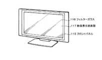
図30は第1適用例となるテレビを示す斜視図である。本適用例に係るテレビは、フロントパネル115やフィルターガラス116等から構成される映像表示画面部117を含み、その映像表示画面部117に上記の液晶表示装置1を適用可能である。 FIG. 30 is a perspective view showing a television as a first application example. The television according to this application example includes a video display screen unit 117 including a front panel 115, a filter glass 116, and the like, and the liquid
図31は第2適用例となるデジタルカメラを示す図であり、(A)は表側から見た斜視図、(B)は裏側から見た斜視図である。本適用例に係るデジタルカメラは、フラッシュ用の発光部111、表示部112、メニュースイッチ113、シャッターボタン114等を含み、その表示部112に上記の液晶表示装置1を適用可能である。 31A and 31B are diagrams showing a digital camera as a second application example, in which FIG. 31A is a perspective view seen from the front side, and FIG. 31B is a perspective view seen from the back side. The digital camera according to this application example includes a light emitting unit 111 for flash, a display unit 112, a menu switch 113, a shutter button 114, and the like, and the liquid
図32は第3適用例となるノート型パーソナルコンピュータを示す斜視図である。本適用例に係るノート型パーソナルコンピュータは、本体121に、文字等を入力するとき操作されるキーボード122、画像を表示する表示部123等を含み、その表示部123に上記の液晶表示装置1を適用可能である。 FIG. 32 is a perspective view showing a notebook personal computer as a third application example. The notebook personal computer according to this application example includes a main body 121 that includes a keyboard 122 that is operated when characters and the like are input, a display unit 123 that displays an image, and the like. Applicable.
図33は第4適用例となるビデオカメラを示す斜視図である。本適用例に係るビデオカメラは、本体部131、前方を向いた側面に被写体撮影用のレンズ132、撮影時のスタート/ストップスイッチ133、表示部134等を含み、その表示部134に上記の液晶表示装置1を適用可能である。 FIG. 33 is a perspective view showing a video camera as a fourth application example. The video camera according to this application example includes a main body 131, a lens 132 for photographing an object on the side facing forward, a start / stop switch 133 at the time of photographing, a display unit 134, and the like. The
図34は第5適用例となる携帯端末装置、例えば携帯電話機を示す図であり、(A)は開いた状態での正面図、(B)はその側面図、(C)は閉じた状態での正面図、(D)は左側面図、(E)は右側面図、(F)は上面図、(G)は下面図である。本適用例に係る携帯電話機は、上側筐体141、下側筐体142、連結部(ここではヒンジ部)143、ディスプレイ144、サブディスプレイ145、ピクチャーライト146、カメラ147等を含み、そのディスプレイ144やサブディスプレイ145に上記の液晶表示装置1を適用可能である。 FIG. 34 is a diagram showing a mobile terminal device, for example, a mobile phone, as a fifth application example, where (A) is a front view in an open state, (B) is a side view thereof, and (C) is in a closed state. (D) is a left side view, (E) is a right side view, (F) is a top view, and (G) is a bottom view. The mobile phone according to this application example includes an upper housing 141, a lower housing 142, a connecting portion (here, a hinge portion) 143, a display 144, a sub display 145, a picture light 146, a camera 147, and the like. In addition, the liquid
1…液晶表示装置、2…駆動基板、3…対向基板、4…液晶層、5,8…ガラス基板、6…画素電極、7,10…偏光板、11…画素、21…第1の素子形成部、22…第2の素子形成部、23,33…ゲート電極、24…ゲート絶縁膜、25…チャネル層、26,36…ソース、27,37…ドレイン、28,38…ソース電極、29,39…ドレイン電極、30…層間絶縁膜、31,32…半導体膜、35…光電変換層、40…光反射膜、41…透明導電膜、E1…表示領域、E2…周辺領域 DESCRIPTION OF
Claims (19)
Translated fromJapanese前記第2の活性層は、前記第1の活性層よりも光吸収率が高い
表示装置。On a base layer of a substrate on which a plurality of pixels are arranged in a matrix, a first active layer that constitutes a switching element of the pixel and a second active layer that constitutes a photosensor element,
The second active layer has a higher light absorption rate than the first active layer.
請求項1記載の表示装置。The display device according to claim 1, wherein the second active layer is formed thicker than the first active layer.
請求項1又は2記載の表示装置。The display device according to claim 1, wherein the second active layer is formed of a material different from that of the first active layer.
請求項2記載の表示装置。The second active layer has a stacked structure including a first layer having the same thickness as the first active layer and a second layer stacked on the first layer. The display device described.
請求項4記載の表示装置。The display device according to claim 4, wherein the second layer is formed using the same element as the first layer.
前記第1の活性層は、前記表示領域及び前記周辺領域のうち、少なくとも前記表示領域に配置され、
前記第2の活性層は、前記表示領域及び前記周辺領域のうち、少なくとも一方の領域に配置されている
請求項1記載の表示装置。The substrate has a display area in which the plurality of pixels are arranged, and a peripheral area adjacent to the display area,
The first active layer is disposed in at least the display area of the display area and the peripheral area,
The display device according to claim 1, wherein the second active layer is disposed in at least one of the display region and the peripheral region.
前記第1の活性層は、透明な半導体膜によって形成されるとともに、前記表示領域に配置され、
前記第2の活性層は、非透明な半導体膜によって形成されるとともに、前記周辺領域に配置されている
請求項1記載の表示装置。The substrate has a display area in which the plurality of pixels are arranged, and a peripheral area adjacent to the display area,
The first active layer is formed of a transparent semiconductor film and is disposed in the display area.
The display device according to claim 1, wherein the second active layer is formed of a non-transparent semiconductor film and disposed in the peripheral region.
請求項1記載の表示装置。The display device according to claim 1, wherein a light reflection film is formed on a surface of an electrode disposed opposite to the side on which external light is incident and closest to the second active layer.
前記1の活性層と同じ前記下地層の上に、光センサ素子を構成する第2の活性層を、前記第1の活性層より光吸収率が高くなるように形成する
表示装置の製造方法。Forming a first active layer constituting a switching element of the pixel on a base layer of a substrate for forming a plurality of pixels in a matrix;
A method for manufacturing a display device, comprising: forming a second active layer constituting an optical sensor element on the same base layer as the first active layer so as to have a light absorption rate higher than that of the first active layer.
請求項9記載の表示装置の製造方法。The method for manufacturing a display device according to claim 9, wherein the second active layer is formed thicker than the first active layer.
請求項9記載の表示装置の製造方法。The method for manufacturing a display device according to claim 9, wherein the second active layer is formed of a material different from that of the first active layer.
前記第1層と、当該第1層の上に積層された第2層とを積層させることにより、前記第2の活性層を形成する
請求項10記載の表示装置の製造方法。Forming a first layer having the same thickness as the first active layer together with the first active layer;
The method for manufacturing a display device according to claim 10, wherein the second active layer is formed by stacking the first layer and a second layer stacked on the first layer.
前記1の活性層と同じ前記下地層の上に、光センサ素子を構成する第2の活性層を、前記第1の活性層と異なる層厚または異なる材料により形成する
表示装置の製造方法。Forming a first active layer constituting a switching element of the pixel on a base layer of a substrate for forming a plurality of pixels in a matrix;
A method for manufacturing a display device, wherein a second active layer constituting an optical sensor element is formed on the same base layer as the first active layer with a layer thickness or a material different from that of the first active layer.
前記不純物を導入した半導体膜を前記第1の素子形成部と前記第2の素子形成部でそれぞれ島状に分離することにより、前記第1の素子形成部に前記半導体膜によって第1の活性層を形成するとともに、前記第2の素子形成部で活性層相当部の半導体膜を除去し、
前記第2の素子形成部で半導体膜を除去した部分に第2の活性層を形成することにより、
前記基板上に前記第1の活性層を含むスイッチング素子と前記第2の活性層を含む光センサ素子を形成する
表示装置の製造方法。After a semiconductor film is formed over the first element formation portion and the second element formation portion on a substrate for forming a plurality of pixels in a matrix, impurities are introduced into the semiconductor film,
The semiconductor film into which the impurity is introduced is separated into island shapes in the first element forming portion and the second element forming portion, respectively, so that a first active layer is formed in the first element forming portion by the semiconductor film. And removing the semiconductor film corresponding to the active layer in the second element formation portion,
By forming a second active layer in the portion where the semiconductor film is removed in the second element formation portion,
A method for manufacturing a display device, comprising: forming a switching element including the first active layer and a photosensor element including the second active layer on the substrate.
請求項14記載の表示装置の製造方法。The method for manufacturing a display device according to claim 14, wherein the second active layer is formed by a selective film forming method of selectively forming a film at least in a portion where the semiconductor film is removed in the second element forming portion. .
前記透明導電膜を前記第1の素子形成部と前記第2の素子形成部でそれぞれ島状に分離することにより、前記第1の素子形成部で活性層相当部の透明導電膜を除去するとともに、前記第2の素子形成部で活性層相当部の透明導電膜を除去し、
前記第1の素子形成部で透明導電膜を除去した部分に透明半導体膜によって第1の活性層を形成するとともに、前記第2の素子形成部で透明導電膜を除去した部分に第2の活性層を形成することにより、
前記基板上に前記第1の活性層を含むスイッチング素子と前記第2の活性層を含む光センサ素子を形成する
表示装置の製造方法。On the substrate for forming a plurality of pixels in a matrix, a transparent conductive film is formed across the first element formation portion and the second element formation portion,
The transparent conductive film is separated into island shapes at the first element forming portion and the second element forming portion, respectively, thereby removing the transparent conductive film corresponding to the active layer at the first element forming portion. Removing the transparent conductive film corresponding to the active layer in the second element forming portion,
A first active layer is formed with a transparent semiconductor film in a portion where the transparent conductive film is removed in the first element formation portion, and a second active layer is formed in a portion where the transparent conductive film is removed in the second element formation portion. By forming a layer,
A method for manufacturing a display device, comprising: forming a switching element including the first active layer and a photosensor element including the second active layer on the substrate.
請求項16記載の表示装置の製造方法。The display device manufacturing method according to claim 16, wherein the second active layer is formed by a selective film forming method in which a film is selectively formed at least in a portion where the transparent conductive film is removed in the second element forming portion. Method.
前記第1半導体膜を覆う状態でマスク層を形成した後、前記第2の素子形成部で活性層相当部の半導体膜の表面が露出するように前記マスク層を部分的に除去し、
前記マスク層を除去した部分に第2半導体膜を積層して形成し、
前記第1半導体膜を前記第1の素子形成部と前記第2の素子形成部でそれぞれ島状に分離することにより、前記第1の素子形成部に前記第1半導体膜によって第1の活性層を形成するとともに、前記第2の素子形成部に前記第1半導体膜と前記第2半導体膜によって第2の活性層を形成することにより、
前記基板上に前記第1の活性層を含むスイッチング素子と前記第2の活性層を含む光センサ素子を形成する
表示装置の製造方法。A polycrystalline first semiconductor film is formed over a first element formation portion and a second element formation portion on a substrate for forming a plurality of pixels in a matrix, and then impurities are introduced into the first semiconductor film. And
After forming a mask layer so as to cover the first semiconductor film, the mask layer is partially removed so that the surface of the semiconductor film corresponding to the active layer is exposed in the second element formation portion,
Forming a second semiconductor film on the portion where the mask layer is removed;
By separating the first semiconductor film into an island shape at each of the first element formation portion and the second element formation portion, a first active layer is formed on the first element formation portion by the first semiconductor film. And forming a second active layer with the first semiconductor film and the second semiconductor film in the second element formation portion,
A method for manufacturing a display device, comprising: forming a switching element including the first active layer and a photosensor element including the second active layer on the substrate.
請求項18記載の表示装置の製造方法。The method for manufacturing a display device according to claim 18, wherein the second active layer is formed by a selective film forming method in which a film is selectively formed at least in a portion where the mask layer is removed.
Priority Applications (6)
| Application Number | Priority Date | Filing Date | Title |
|---|---|---|---|
| JP2008216975AJP5567770B2 (en) | 2007-09-21 | 2008-08-26 | Display device and manufacturing method of display device |
| KR1020097019412AKR101471221B1 (en) | 2007-09-21 | 2008-09-18 | Display device and manufacturing method of display device |
| CN200880009062.1ACN101636691B (en) | 2007-09-21 | 2008-09-18 | Display device and method for manufacturing display device |
| US12/530,801US8619208B2 (en) | 2007-09-21 | 2008-09-18 | Display and method for manufacturing display |
| PCT/JP2008/066815WO2009038111A1 (en) | 2007-09-21 | 2008-09-18 | Display device and method for manufacturing display device |
| TW097136227ATWI482134B (en) | 2007-09-21 | 2008-09-19 | Display device and display device |
Applications Claiming Priority (3)
| Application Number | Priority Date | Filing Date | Title |
|---|---|---|---|
| JP2007244880 | 2007-09-21 | ||
| JP2007244880 | 2007-09-21 | ||
| JP2008216975AJP5567770B2 (en) | 2007-09-21 | 2008-08-26 | Display device and manufacturing method of display device |
Publications (3)
| Publication Number | Publication Date |
|---|---|
| JP2009093154Atrue JP2009093154A (en) | 2009-04-30 |
| JP2009093154A5 JP2009093154A5 (en) | 2011-08-11 |
| JP5567770B2 JP5567770B2 (en) | 2014-08-06 |
Family
ID=40665162
Family Applications (1)
| Application Number | Title | Priority Date | Filing Date |
|---|---|---|---|
| JP2008216975AExpired - Fee RelatedJP5567770B2 (en) | 2007-09-21 | 2008-08-26 | Display device and manufacturing method of display device |
Country Status (5)
| Country | Link |
|---|---|
| US (1) | US8619208B2 (en) |
| JP (1) | JP5567770B2 (en) |
| KR (1) | KR101471221B1 (en) |
| CN (1) | CN101636691B (en) |
| TW (1) | TWI482134B (en) |
Cited By (17)
| Publication number | Priority date | Publication date | Assignee | Title |
|---|---|---|---|---|
| WO2011045956A1 (en)* | 2009-10-16 | 2011-04-21 | シャープ株式会社 | Semiconductor device, display device provided with same, and method for manufacturing semiconductor device |
| JP2011102960A (en)* | 2009-11-10 | 2011-05-26 | Samsung Mobile Display Co Ltd | Organic light emitting diode display and method for manufacturing the same |
| JP2011210248A (en)* | 2010-03-11 | 2011-10-20 | Semiconductor Energy Lab Co Ltd | Semiconductor device |
| JP2012005102A (en)* | 2010-06-15 | 2012-01-05 | Ind Technol Res Inst | Active photosensor pixel, active photosensor array, and photo-sensing method |
| JP2014240983A (en)* | 2009-11-06 | 2014-12-25 | 株式会社半導体エネルギー研究所 | Display device |
| JP2015015043A (en)* | 2009-08-24 | 2015-01-22 | 株式会社半導体エネルギー研究所 | Display device |
| JP2015092360A (en)* | 2010-03-08 | 2015-05-14 | 株式会社半導体エネルギー研究所 | Display device |
| US9214508B2 (en) | 2014-02-24 | 2015-12-15 | Lg Display Co., Ltd. | Thin film transistor substrate with intermediate insulating layer and display using the same |
| JP2015228032A (en)* | 2009-09-04 | 2015-12-17 | 株式会社半導体エネルギー研究所 | Semiconductor device |
| JP2017103463A (en)* | 2009-08-07 | 2017-06-08 | 株式会社半導体エネルギー研究所 | Semiconductor device |
| US9691799B2 (en) | 2014-02-24 | 2017-06-27 | Lg Display Co., Ltd. | Thin film transistor substrate and display using the same |
| US9721973B2 (en) | 2014-02-24 | 2017-08-01 | Lg Display Co., Ltd. | Thin film transistor substrate and display using the same |
| US9881986B2 (en) | 2014-02-24 | 2018-01-30 | Lg Display Co., Ltd. | Thin film transistor substrate and display using the same |
| US10186528B2 (en) | 2014-02-24 | 2019-01-22 | Lg Display Co., Ltd. | Thin film transistor substrate and display using the same |
| US10325937B2 (en) | 2014-02-24 | 2019-06-18 | Lg Display Co., Ltd. | Thin film transistor substrate with intermediate insulating layer and display using the same |
| US10903246B2 (en) | 2014-02-24 | 2021-01-26 | Lg Display Co., Ltd. | Thin film transistor substrate and display using the same |
| US10985196B2 (en) | 2014-02-24 | 2021-04-20 | Lg Display Co., Ltd. | Thin film transistor substrate with intermediate insulating layer and display using the same |
Families Citing this family (22)
| Publication number | Priority date | Publication date | Assignee | Title |
|---|---|---|---|---|
| TWI627757B (en)* | 2008-07-31 | 2018-06-21 | 半導體能源研究所股份有限公司 | Semiconductor device |
| JP2010056541A (en) | 2008-07-31 | 2010-03-11 | Semiconductor Energy Lab Co Ltd | Semiconductor device and manufacturing method thereof |
| US20120001190A1 (en)* | 2009-05-12 | 2012-01-05 | Sharp Kabushiki Kaisha | Thin film transistor and method of fabricating same |
| US9111810B2 (en)* | 2010-04-30 | 2015-08-18 | Sharp Kabushiki Kaisha | Circuit board and display device including first and second channel layers made of different semiconductor materials |
| CN102870220B (en)* | 2010-04-30 | 2014-05-07 | 夏普株式会社 | Circuit board and display device |
| CN102376276B (en)* | 2010-08-05 | 2013-11-20 | 财团法人工业技术研究院 | Active light sensing pixel, active light sensing array and light sensing method |
| KR101822406B1 (en) | 2011-08-29 | 2018-01-29 | 삼성디스플레이 주식회사 | Touch substrate and method of manufacturing the same |
| KR101506303B1 (en) | 2011-09-29 | 2015-03-26 | 가부시키가이샤 한도오따이 에네루기 켄큐쇼 | Semiconductor device and method for manufacturing the same |
| JP2014116429A (en)* | 2012-12-07 | 2014-06-26 | Japan Display Inc | Image-capturing device and image display system |
| KR102068275B1 (en) | 2012-12-20 | 2020-01-21 | 삼성디스플레이 주식회사 | Thin film transistor array panel and manufacturing method thereof |
| KR102091444B1 (en)* | 2013-10-08 | 2020-03-23 | 삼성디스플레이 주식회사 | Display substrate and method of manufacturing a display substrate |
| JP2015158572A (en)* | 2014-02-24 | 2015-09-03 | 株式会社Joled | Display device, electronic apparatus |
| CN104716196B (en)* | 2015-03-18 | 2017-08-08 | 京东方科技集团股份有限公司 | Thin film transistor (TFT) and preparation method thereof, array base palte and display device |
| CN105244404B (en)* | 2015-10-19 | 2018-02-06 | 昆山龙腾光电有限公司 | Integrated optic-electronic sensor |
| CN106326845B (en)* | 2016-08-15 | 2017-08-11 | 京东方科技集团股份有限公司 | Fingerprint identification unit and preparation method, array base palte, display device and fingerprint identification method |
| US10367017B2 (en)* | 2017-11-22 | 2019-07-30 | Shenzhen China Star Optoelectronics Semiconductor Display Technology Co., Ltd. | Array substrate and manufacturing method thereof |
| CN107946244B (en)* | 2017-11-22 | 2020-08-04 | 深圳市华星光电半导体显示技术有限公司 | Array substrate and preparation method thereof |
| CN107978610B (en)* | 2017-11-30 | 2020-04-24 | 上海天马微电子有限公司 | Array substrate, display panel, display device and manufacturing method of array substrate |
| TWI721776B (en)* | 2020-02-06 | 2021-03-11 | 友達光電股份有限公司 | Active device substrate and manufactturing method thereof |
| CN111522181B (en)* | 2020-04-27 | 2023-05-05 | 深圳市华星光电半导体显示技术有限公司 | A kind of array substrate, display panel and preparation method thereof |
| KR102849288B1 (en)* | 2020-06-01 | 2025-08-22 | 삼성전자주식회사 | Flash led package |
| CN112599630B (en) | 2020-12-07 | 2022-06-10 | Tcl华星光电技术有限公司 | Light Sensors and Display Devices |
Citations (3)
| Publication number | Priority date | Publication date | Assignee | Title |
|---|---|---|---|---|
| JPH1090655A (en)* | 1996-09-17 | 1998-04-10 | Toshiba Corp | Display device |
| US20030122165A1 (en)* | 2000-08-31 | 2003-07-03 | Lg.Philips Lcd Co., Ltd. | TFT type optical detecting sensor implementing different TFTs and the fabricating method thereof |
| JP2005043672A (en)* | 2003-07-22 | 2005-02-17 | Toshiba Matsushita Display Technology Co Ltd | Array substrate and manufacturing method thereof |
Family Cites Families (5)
| Publication number | Priority date | Publication date | Assignee | Title |
|---|---|---|---|---|
| US6362507B1 (en)* | 1999-04-20 | 2002-03-26 | Semiconductor Energy Laboratory Co., Ltd. | Electro-optical devices in which pixel section and the driver circuit are disposed over the same substrate |
| US7385223B2 (en)* | 2003-04-24 | 2008-06-10 | Samsung Sdi Co., Ltd. | Flat panel display with thin film transistor |
| KR100585410B1 (en)* | 2003-11-11 | 2006-06-07 | 엘지.필립스 엘시디 주식회사 | Switching element and driving element of liquid crystal display device with integrated driving circuit and manufacturing method thereof |
| TWI255032B (en)* | 2004-01-29 | 2006-05-11 | Casio Computer Co Ltd | Transistor array and manufacturing method thereof image processing device |
| EP1739000B1 (en) | 2005-06-27 | 2011-08-10 | Campagnolo S.R.L. | Control device for a bicycle derailleur |
- 2008
- 2008-08-26JPJP2008216975Apatent/JP5567770B2/ennot_activeExpired - Fee Related
- 2008-09-18CNCN200880009062.1Apatent/CN101636691B/ennot_activeExpired - Fee Related
- 2008-09-18USUS12/530,801patent/US8619208B2/enactiveActive
- 2008-09-18KRKR1020097019412Apatent/KR101471221B1/ennot_activeExpired - Fee Related
- 2008-09-19TWTW097136227Apatent/TWI482134B/enactive
Patent Citations (3)
| Publication number | Priority date | Publication date | Assignee | Title |
|---|---|---|---|---|
| JPH1090655A (en)* | 1996-09-17 | 1998-04-10 | Toshiba Corp | Display device |
| US20030122165A1 (en)* | 2000-08-31 | 2003-07-03 | Lg.Philips Lcd Co., Ltd. | TFT type optical detecting sensor implementing different TFTs and the fabricating method thereof |
| JP2005043672A (en)* | 2003-07-22 | 2005-02-17 | Toshiba Matsushita Display Technology Co Ltd | Array substrate and manufacturing method thereof |
Cited By (29)
| Publication number | Priority date | Publication date | Assignee | Title |
|---|---|---|---|---|
| JP2017103463A (en)* | 2009-08-07 | 2017-06-08 | 株式会社半導体エネルギー研究所 | Semiconductor device |
| US9954005B2 (en) | 2009-08-07 | 2018-04-24 | Semiconductor Energy Laboratory Co., Ltd. | Semiconductor device comprising oxide semiconductor layer |
| JP2018120231A (en)* | 2009-08-07 | 2018-08-02 | 株式会社半導体エネルギー研究所 | Display device |
| JP2015015043A (en)* | 2009-08-24 | 2015-01-22 | 株式会社半導体エネルギー研究所 | Display device |
| US9542022B2 (en) | 2009-08-24 | 2017-01-10 | Semiconductor Energy Laboratory Co., Ltd. | Touch sensor and method for driving the same and display device |
| JP2016095886A (en)* | 2009-08-24 | 2016-05-26 | 株式会社半導体エネルギー研究所 | Display device |
| JP2015228032A (en)* | 2009-09-04 | 2015-12-17 | 株式会社半導体エネルギー研究所 | Semiconductor device |
| WO2011045956A1 (en)* | 2009-10-16 | 2011-04-21 | シャープ株式会社 | Semiconductor device, display device provided with same, and method for manufacturing semiconductor device |
| US9639211B2 (en) | 2009-11-06 | 2017-05-02 | Semiconductor Energy Laboratory Co., Ltd. | Display device |
| JP2014240983A (en)* | 2009-11-06 | 2014-12-25 | 株式会社半導体エネルギー研究所 | Display device |
| US9368541B2 (en) | 2009-11-06 | 2016-06-14 | Semiconductor Energy Laboratory Co., Ltd. | Display device |
| US9257495B2 (en) | 2009-11-10 | 2016-02-09 | Samsung Display Co., Ltd. | Organic light emitting diode display and method for manufacturing the same |
| US8933868B2 (en) | 2009-11-10 | 2015-01-13 | Samsung Display Co., Ltd. | Organic light emitting diode display and method for manufacturing the same |
| JP2011102960A (en)* | 2009-11-10 | 2011-05-26 | Samsung Mobile Display Co Ltd | Organic light emitting diode display and method for manufacturing the same |
| JP2015092360A (en)* | 2010-03-08 | 2015-05-14 | 株式会社半導体エネルギー研究所 | Display device |
| JP2017084375A (en)* | 2010-03-08 | 2017-05-18 | 株式会社半導体エネルギー研究所 | Display device |
| JP2011210248A (en)* | 2010-03-11 | 2011-10-20 | Semiconductor Energy Lab Co Ltd | Semiconductor device |
| US10031622B2 (en) | 2010-03-11 | 2018-07-24 | Semiconductor Energy Laboratory Co., Ltd. | Semiconductor device |
| US8717335B2 (en) | 2010-06-15 | 2014-05-06 | Industrial Technology Research Institute | Active photosensing pixel |
| JP2012005102A (en)* | 2010-06-15 | 2012-01-05 | Ind Technol Res Inst | Active photosensor pixel, active photosensor array, and photo-sensing method |
| US9455279B2 (en) | 2014-02-24 | 2016-09-27 | Lg Display Co., Ltd. | Thin film transistor substrate and display using the same |
| US9881986B2 (en) | 2014-02-24 | 2018-01-30 | Lg Display Co., Ltd. | Thin film transistor substrate and display using the same |
| US9721973B2 (en) | 2014-02-24 | 2017-08-01 | Lg Display Co., Ltd. | Thin film transistor substrate and display using the same |
| US9691799B2 (en) | 2014-02-24 | 2017-06-27 | Lg Display Co., Ltd. | Thin film transistor substrate and display using the same |
| US9214508B2 (en) | 2014-02-24 | 2015-12-15 | Lg Display Co., Ltd. | Thin film transistor substrate with intermediate insulating layer and display using the same |
| US10186528B2 (en) | 2014-02-24 | 2019-01-22 | Lg Display Co., Ltd. | Thin film transistor substrate and display using the same |
| US10325937B2 (en) | 2014-02-24 | 2019-06-18 | Lg Display Co., Ltd. | Thin film transistor substrate with intermediate insulating layer and display using the same |
| US10903246B2 (en) | 2014-02-24 | 2021-01-26 | Lg Display Co., Ltd. | Thin film transistor substrate and display using the same |
| US10985196B2 (en) | 2014-02-24 | 2021-04-20 | Lg Display Co., Ltd. | Thin film transistor substrate with intermediate insulating layer and display using the same |
Also Published As
| Publication number | Publication date |
|---|---|
| US20100171120A1 (en) | 2010-07-08 |
| CN101636691A (en) | 2010-01-27 |
| JP5567770B2 (en) | 2014-08-06 |
| KR20100057528A (en) | 2010-05-31 |
| TW200929119A (en) | 2009-07-01 |
| KR101471221B1 (en) | 2014-12-09 |
| CN101636691B (en) | 2014-05-07 |
| US8619208B2 (en) | 2013-12-31 |
| TWI482134B (en) | 2015-04-21 |
Similar Documents
| Publication | Publication Date | Title |
|---|---|---|
| JP5567770B2 (en) | Display device and manufacturing method of display device | |
| JP5143514B2 (en) | Display device and manufacturing method of display device | |
| TWI453805B (en) | Display and its making method | |
| JP4271268B2 (en) | Image sensor and image sensor integrated active matrix display device | |
| JP4044187B2 (en) | Active matrix display device and manufacturing method thereof | |
| JP2025133764A (en) | display device | |
| JP5351282B2 (en) | Semiconductor device and manufacturing method thereof | |
| CN101577285A (en) | Image display system and method for manufacturing the same | |
| JP2009135188A (en) | Optical sensor and display device | |
| WO2005104234A1 (en) | Image pickup function solid type display device | |
| JP2008153427A (en) | High-sensitivity photosensor element and photosensor device using the same | |
| WO2010095401A1 (en) | Semiconductor device and display device | |
| JP4700659B2 (en) | Liquid crystal display | |
| JP5183173B2 (en) | Optical sensor and display device | |
| JP5025596B2 (en) | Image sensor | |
| JP5604579B2 (en) | Display device | |
| JP2005107383A (en) | Liquid crystal display device | |
| JP5138107B2 (en) | Image sensors, electronic devices | |
| JP2006186266A (en) | Photoelectric conversion element and display device using the same | |
| JP5622812B2 (en) | Display device | |
| JP4999979B2 (en) | Image sensor and electronic device | |
| JP5100799B2 (en) | Liquid crystal display | |
| JP2007188017A (en) | Display device |
Legal Events
| Date | Code | Title | Description |
|---|---|---|---|
| A521 | Request for written amendment filed | Free format text:JAPANESE INTERMEDIATE CODE: A821 Effective date:20091014 | |
| RD02 | Notification of acceptance of power of attorney | Free format text:JAPANESE INTERMEDIATE CODE: A7422 Effective date:20091014 | |
| RD04 | Notification of resignation of power of attorney | Free format text:JAPANESE INTERMEDIATE CODE: A7424 Effective date:20091030 | |
| A521 | Request for written amendment filed | Free format text:JAPANESE INTERMEDIATE CODE: A523 Effective date:20110627 | |
| A621 | Written request for application examination | Free format text:JAPANESE INTERMEDIATE CODE: A621 Effective date:20110627 | |
| A711 | Notification of change in applicant | Free format text:JAPANESE INTERMEDIATE CODE: A711 Effective date:20120330 | |
| A131 | Notification of reasons for refusal | Free format text:JAPANESE INTERMEDIATE CODE: A131 Effective date:20130122 | |
| A521 | Request for written amendment filed | Free format text:JAPANESE INTERMEDIATE CODE: A523 Effective date:20130315 | |
| RD03 | Notification of appointment of power of attorney | Free format text:JAPANESE INTERMEDIATE CODE: A7423 Effective date:20130328 | |
| A131 | Notification of reasons for refusal | Free format text:JAPANESE INTERMEDIATE CODE: A131 Effective date:20131203 | |
| A521 | Request for written amendment filed | Free format text:JAPANESE INTERMEDIATE CODE: A523 Effective date:20140130 | |
| A711 | Notification of change in applicant | Free format text:JAPANESE INTERMEDIATE CODE: A712 Effective date:20140130 | |
| TRDD | Decision of grant or rejection written | ||
| A01 | Written decision to grant a patent or to grant a registration (utility model) | Free format text:JAPANESE INTERMEDIATE CODE: A01 Effective date:20140610 | |
| A61 | First payment of annual fees (during grant procedure) | Free format text:JAPANESE INTERMEDIATE CODE: A61 Effective date:20140620 | |
| R150 | Certificate of patent or registration of utility model | Ref document number:5567770 Country of ref document:JP Free format text:JAPANESE INTERMEDIATE CODE: R150 | |
| LAPS | Cancellation because of no payment of annual fees |