JP2009081943A - Power transmission control device, power transmission device, power transmission side device, and non-contact power transmission system - Google Patents
Power transmission control device, power transmission device, power transmission side device, and non-contact power transmission systemDownload PDFInfo
- Publication number
- JP2009081943A JP2009081943AJP2007249375AJP2007249375AJP2009081943AJP 2009081943 AJP2009081943 AJP 2009081943AJP 2007249375 AJP2007249375 AJP 2007249375AJP 2007249375 AJP2007249375 AJP 2007249375AJP 2009081943 AJP2009081943 AJP 2009081943A
- Authority
- JP
- Japan
- Prior art keywords
- power transmission
- coil
- primary coil
- control circuit
- primary
- Prior art date
- Legal status (The legal status is an assumption and is not a legal conclusion. Google has not performed a legal analysis and makes no representation as to the accuracy of the status listed.)
- Withdrawn
Links
- 230000005540biological transmissionEffects0.000titleclaimsabstractdescription218
- 238000001514detection methodMethods0.000claimsabstractdescription61
- 230000007274generation of a signal involved in cell-cell signalingEffects0.000claimsabstractdescription7
- 238000013459approachMethods0.000claimsdescription34
- 230000033001locomotionEffects0.000claimsdescription15
- 239000000696magnetic materialSubstances0.000claimsdescription11
- 230000007423decreaseEffects0.000claimsdescription9
- 238000013461designMethods0.000abstractdescription9
- 238000010586diagramMethods0.000description20
- 230000004907fluxEffects0.000description15
- 238000000034methodMethods0.000description12
- 230000010355oscillationEffects0.000description10
- 230000008859changeEffects0.000description7
- 238000012986modificationMethods0.000description6
- 230000004048modificationEffects0.000description6
- 230000000694effectsEffects0.000description4
- 239000003990capacitorSubstances0.000description3
- 238000004891communicationMethods0.000description3
- 230000006698inductionEffects0.000description3
- 238000012545processingMethods0.000description3
- 238000004804windingMethods0.000description3
- XEEYBQQBJWHFJM-UHFFFAOYSA-NIronChemical compound[Fe]XEEYBQQBJWHFJM-UHFFFAOYSA-N0.000description2
- 238000006243chemical reactionMethods0.000description2
- 230000001276controlling effectEffects0.000description2
- 239000010438graniteSubstances0.000description2
- 238000009434installationMethods0.000description2
- 239000000463materialSubstances0.000description2
- 230000007246mechanismEffects0.000description2
- 241001125929Trisopterus luscusSpecies0.000description1
- 230000002159abnormal effectEffects0.000description1
- NIXOWILDQLNWCW-UHFFFAOYSA-Nacrylic acid groupChemical groupC(C=C)(=O)ONIXOWILDQLNWCW-UHFFFAOYSA-N0.000description1
- 230000009471actionEffects0.000description1
- 229910052782aluminiumInorganic materials0.000description1
- XAGFODPZIPBFFR-UHFFFAOYSA-NaluminiumChemical compound[Al]XAGFODPZIPBFFR-UHFFFAOYSA-N0.000description1
- 230000001413cellular effectEffects0.000description1
- 239000000919ceramicSubstances0.000description1
- 239000003086colorantSubstances0.000description1
- 230000008878couplingEffects0.000description1
- 238000010168coupling processMethods0.000description1
- 238000005859coupling reactionMethods0.000description1
- 239000013078crystalSubstances0.000description1
- 230000003247decreasing effectEffects0.000description1
- 230000026058directional locomotionEffects0.000description1
- 230000005674electromagnetic inductionEffects0.000description1
- 238000005516engineering processMethods0.000description1
- 230000020169heat generationEffects0.000description1
- 238000003780insertionMethods0.000description1
- 230000037431insertionEffects0.000description1
- 229910052742ironInorganic materials0.000description1
- 239000004973liquid crystal related substanceSubstances0.000description1
- 229910052751metalInorganic materials0.000description1
- 239000002184metalSubstances0.000description1
- 238000012544monitoring processMethods0.000description1
- 230000008569processEffects0.000description1
- 230000001105regulatory effectEffects0.000description1
- 230000004044responseEffects0.000description1
- 238000012546transferMethods0.000description1
Images


Classifications
- H—ELECTRICITY
- H02—GENERATION; CONVERSION OR DISTRIBUTION OF ELECTRIC POWER
- H02J—CIRCUIT ARRANGEMENTS OR SYSTEMS FOR SUPPLYING OR DISTRIBUTING ELECTRIC POWER; SYSTEMS FOR STORING ELECTRIC ENERGY
- H02J7/00—Circuit arrangements for charging or depolarising batteries or for supplying loads from batteries
- H02J7/0042—Circuit arrangements for charging or depolarising batteries or for supplying loads from batteries characterised by the mechanical construction
- H—ELECTRICITY
- H02—GENERATION; CONVERSION OR DISTRIBUTION OF ELECTRIC POWER
- H02J—CIRCUIT ARRANGEMENTS OR SYSTEMS FOR SUPPLYING OR DISTRIBUTING ELECTRIC POWER; SYSTEMS FOR STORING ELECTRIC ENERGY
- H02J50/00—Circuit arrangements or systems for wireless supply or distribution of electric power
- H02J50/10—Circuit arrangements or systems for wireless supply or distribution of electric power using inductive coupling
- H02J50/12—Circuit arrangements or systems for wireless supply or distribution of electric power using inductive coupling of the resonant type
- H—ELECTRICITY
- H02—GENERATION; CONVERSION OR DISTRIBUTION OF ELECTRIC POWER
- H02J—CIRCUIT ARRANGEMENTS OR SYSTEMS FOR SUPPLYING OR DISTRIBUTING ELECTRIC POWER; SYSTEMS FOR STORING ELECTRIC ENERGY
- H02J50/00—Circuit arrangements or systems for wireless supply or distribution of electric power
- H02J50/60—Circuit arrangements or systems for wireless supply or distribution of electric power responsive to the presence of foreign objects, e.g. detection of living beings
- H—ELECTRICITY
- H02—GENERATION; CONVERSION OR DISTRIBUTION OF ELECTRIC POWER
- H02J—CIRCUIT ARRANGEMENTS OR SYSTEMS FOR SUPPLYING OR DISTRIBUTING ELECTRIC POWER; SYSTEMS FOR STORING ELECTRIC ENERGY
- H02J50/00—Circuit arrangements or systems for wireless supply or distribution of electric power
- H02J50/70—Circuit arrangements or systems for wireless supply or distribution of electric power involving the reduction of electric, magnetic or electromagnetic leakage fields
- H—ELECTRICITY
- H02—GENERATION; CONVERSION OR DISTRIBUTION OF ELECTRIC POWER
- H02J—CIRCUIT ARRANGEMENTS OR SYSTEMS FOR SUPPLYING OR DISTRIBUTING ELECTRIC POWER; SYSTEMS FOR STORING ELECTRIC ENERGY
- H02J50/00—Circuit arrangements or systems for wireless supply or distribution of electric power
- H02J50/80—Circuit arrangements or systems for wireless supply or distribution of electric power involving the exchange of data, concerning supply or distribution of electric power, between transmitting devices and receiving devices
- H—ELECTRICITY
- H02—GENERATION; CONVERSION OR DISTRIBUTION OF ELECTRIC POWER
- H02J—CIRCUIT ARRANGEMENTS OR SYSTEMS FOR SUPPLYING OR DISTRIBUTING ELECTRIC POWER; SYSTEMS FOR STORING ELECTRIC ENERGY
- H02J50/00—Circuit arrangements or systems for wireless supply or distribution of electric power
- H02J50/90—Circuit arrangements or systems for wireless supply or distribution of electric power involving detection or optimisation of position, e.g. alignment
- H—ELECTRICITY
- H02—GENERATION; CONVERSION OR DISTRIBUTION OF ELECTRIC POWER
- H02J—CIRCUIT ARRANGEMENTS OR SYSTEMS FOR SUPPLYING OR DISTRIBUTING ELECTRIC POWER; SYSTEMS FOR STORING ELECTRIC ENERGY
- H02J7/00—Circuit arrangements for charging or depolarising batteries or for supplying loads from batteries
- H02J7/00032—Circuit arrangements for charging or depolarising batteries or for supplying loads from batteries characterised by data exchange
- H02J7/00036—Charger exchanging data with battery
- H—ELECTRICITY
- H02—GENERATION; CONVERSION OR DISTRIBUTION OF ELECTRIC POWER
- H02J—CIRCUIT ARRANGEMENTS OR SYSTEMS FOR SUPPLYING OR DISTRIBUTING ELECTRIC POWER; SYSTEMS FOR STORING ELECTRIC ENERGY
- H02J7/00—Circuit arrangements for charging or depolarising batteries or for supplying loads from batteries
- H02J7/00047—Circuit arrangements for charging or depolarising batteries or for supplying loads from batteries with provisions for charging different types of batteries
Landscapes
- Engineering & Computer Science (AREA)
- Power Engineering (AREA)
- Computer Networks & Wireless Communication (AREA)
- Physics & Mathematics (AREA)
- Electromagnetism (AREA)
- Charge And Discharge Circuits For Batteries Or The Like (AREA)
- Dc-Dc Converters (AREA)
Abstract
Translated fromJapaneseDescription
Translated fromJapanese本発明は、送電制御装置、送電装置、送電側装置および無接点電力伝送システム等に関する。 The present invention relates to a power transmission control device, a power transmission device, a power transmission side device, a contactless power transmission system, and the like.
近年、電磁誘導を利用し、金属部分の接点がなくても電力伝送を可能にする無接点電力伝送(非接触電力伝送)が脚光を浴びている、この無接点電力伝送の適用例として、携帯電話機や家庭用機器(例えば電話機の子機や時計)の充電などが提案されている。 In recent years, contactless power transmission (contactless power transmission) that uses electromagnetic induction and enables power transmission even without a metal part contact has been highlighted. Charging of telephones and household devices (for example, telephone handsets and watches) has been proposed.
1次コイルと2次コイルを用いた無接点電力伝送装置は、例えば、特許文献1に記載されている。 A non-contact power transmission device using a primary coil and a secondary coil is described in
また、無接点電力伝送システムにおいて、1次コイルと2次コイルとの位置ずれを検出する技術は、特許文献2に記載されている。特許文献2に記載の技術では、受電装置の整流回路の出力電圧に基づいて、1次コイルと2次コイルの相対位置関係が正常であるか否かを検出し、正常である場合にその旨を発光ダイオードLEDの点灯により使用者に知らせる。位置関係が異常である場合にはLEDが点灯しない。この場合には、ユーザが手動で位置関係を調整する。
無接点電力伝送システムにおいて、1次コイルと2次コイルとの位置合わせを正確に行うためには、例えば、受電装置を内蔵する2次側機器に専用の送電台(送電装置を内蔵する1次側電子機器)を使用するのがよい。但し、この場合は、2次側機器が異なれば、その都度、専用の送電台を用意する必要が生じて、送電台の汎用性を担保することができない。 In order to accurately align the primary coil and the secondary coil in the non-contact power transmission system, for example, a dedicated power transmission stand (primary with a built-in power transmission device) is installed in a secondary side device with a built-in power receiving device. Side electronic equipment). However, in this case, if the secondary side equipment is different, it is necessary to prepare a dedicated power transmission stand each time, and the versatility of the power transmission stand cannot be ensured.
例えば、無接点電力伝送システムを利用して携帯端末のバッテリを充電する場合、例えば、同じ大きさの端末であっても、メーカが異なれば、外観の形状(デザイン)が異なり、かつ、2次コイルの設置位置も異なるのが普通であり、一台の送電台(充電台)で、異なるメーカの複数の携帯端末に対応することは困難である。 For example, when charging a battery of a portable terminal using a non-contact power transmission system, for example, even if the terminal has the same size, the shape (design) of the appearance is different if the manufacturer is different, and the secondary Coil installation positions are usually different, and it is difficult to handle a plurality of portable terminals from different manufacturers with a single power transmission stand (charging stand).
また、種類の異なる端末(例えば、携帯電話端末とPDA端末)では、端末の大きさや形状(デザイン)が異なり、2次コイルの設置位置も異なる。よって、同様に、1台の送電台で、種類の異なる端末に対応することは困難である。 In addition, terminals of different types (for example, a mobile phone terminal and a PDA terminal) have different terminal sizes and shapes (designs), and the installation positions of the secondary coils are also different. Therefore, similarly, it is difficult to handle different types of terminals with a single power transmission stand.
また、専用の送電台を使用せずに、例えば、フラットな平面をもつ構造物(例えば机)の所定エリア上に携帯端末を載置するだけで充電が可能となれば、無接点電力伝送システムの利便性は格段に向上する。しかし、所定のエリア上の概略位置に置かれた携帯端末の2次コイルの正確な位置は、上記と同様の理由で特定することができない。よって、このような次世代の無接点電力伝送システムは、現状の技術では実現できない。 In addition, if charging can be performed simply by placing a mobile terminal on a predetermined area of a structure (for example, a desk) having a flat plane without using a dedicated power transmission stand, a non-contact power transmission system Convenience is greatly improved. However, the exact position of the secondary coil of the mobile terminal placed at the approximate position on the predetermined area cannot be specified for the same reason as described above. Therefore, such a next-generation contactless power transmission system cannot be realized with the current technology.
特許文献2の技術では、1次コイルと2次コイルとの位置合わせが正確であるか否かをユーザに提示することはできるが、位置合わせは、結局のところ、ユーザの手動による調整に頼るしかない。 In the technique of Patent Document 2, although it is possible to present to the user whether or not the alignment between the primary coil and the secondary coil is accurate, the alignment ultimately depends on the user's manual adjustment. There is only.
本発明はこのような考察に基づいてなされたものである。本発明の少なくとも一つの実施形態では、1次コイルと2次コイルの自動的な位置合わせが可能となり、2次側機器のメーカ、大きさ、種類、機器デザイン等に依存せずに、常に両コイルの相対位置を自動的に適正化することができる。よって、汎用性が高い送電装置(1次側装置)が実現され、次世代の無接点電力伝送システムも実現される。 The present invention has been made based on such consideration. In at least one embodiment of the present invention, automatic alignment of the primary coil and the secondary coil is possible, and both of them are always used without depending on the manufacturer, size, type, device design, etc. of the secondary device. The relative position of the coil can be automatically optimized. Therefore, a highly versatile power transmission device (primary side device) is realized, and a next-generation contactless power transmission system is also realized.
(1)本発明の送電制御装置の一態様は、送電装置から受電装置に対して、電磁結合された1次コイルおよび2次コイルを経由して無接点で電力を伝送する無接点電力伝送システムにおける、前記送電装置に設けられる送電制御装置であって、前記受電装置への送電を制御する送電側制御回路と、前記1次コイルのXY平面上における位置を移動させるためのアクチュエータの動作を制御するアクチュエータ制御回路と、前記1次コイルのコイル端電圧またはコイル電流に基づいて、前記1次コイルと前記2次コイルの相対位置検出信号を生成する相対位置検出信号生成回路と、前記相対位置検出信号が示す前記1次コイルと前記2次コイルの相対位置が許容範囲になるように、前記アクチュエータ制御回路に指示して前記1次コイルのXY平面上における位置を移動させる1次コイル位置制御回路と、を有する。 (1) One aspect of the power transmission control device of the present invention is a non-contact power transmission system that transmits power from a power transmission device to a power reception device in a contactless manner via an electromagnetically coupled primary coil and secondary coil. A power transmission control device provided in the power transmission device for controlling a power transmission side control circuit for controlling power transmission to the power reception device and an operation of an actuator for moving a position of the primary coil on the XY plane. A relative position detection signal generation circuit that generates a relative position detection signal between the primary coil and the secondary coil based on a coil end voltage or a coil current of the primary coil, and the relative position detection XY of the primary coil is instructed to the actuator control circuit so that the relative position of the primary coil and the secondary coil indicated by the signal falls within an allowable range. Having a primary coil position control circuit for moving the position on the plane.
送電制御装置は、送電側制御回路による送電制御機能に加えて、アクチュエータ制御回路によるアクチュエータ制御機能を有している。コイル端電圧またはコイル電流に基づいて相対位置検出信号生成回路が、1次コイルと受電側の2次コイルとの相対的位置関係を示す相対位置検出信号を生成する。アクチュエータ制御回路は、相対位置検出信号を指標として、1次コイルと2次コイルの相対的な位置関係が許容範囲になるように、アクチュエータを動作させて1次コイルのXY平面における位置を調整する。2次側機器が概略の位置に置かれたとしても、1次コイルが自動的に最適位置に移動するため、常に適正な送電が実現される。2次側機器の大きさ、形状、機器デザイン等に影響されず、常に適正な送電が実現されるため、無接点電力伝送システムの汎用性が格段に向上する。また、2次側機器の設計の自由度は何ら制限されないため、2次側機器のメーカの負担が生じない。
相対位置検出信号生成回路は、例えば、コイル端電圧のピーク値を所定のしきい値電圧と比較することによって得られる。このような回路は、無接点電力伝送システムにおいて、例えば、1次側と2次側の通信を可能とするために元々、備わっている回路(あるいは、元々の回路に若干の変更を施すだけで実現できる回路)である。特別な回路(位置検出素子等)を用いず、無接点電力伝送システムに備わっている回路構成を活用してコイル間の相対的な位置関係を検出するため、構成が複雑化せず、かつ実現が容易である。なお、一次コイル位置制御回路は、送電側制御回路(主として送電を制御する回路)内に設けることができ、また、アクチュエータ制御回路内に設けることもでき、あるいは、それらの回路とは別に設けることもできる。The power transmission control device has an actuator control function by an actuator control circuit in addition to a power transmission control function by a power transmission side control circuit. Based on the coil end voltage or the coil current, the relative position detection signal generation circuit generates a relative position detection signal indicating the relative positional relationship between the primary coil and the power receiving side secondary coil. The actuator control circuit adjusts the position of the primary coil in the XY plane by operating the actuator so that the relative positional relationship between the primary coil and the secondary coil falls within an allowable range using the relative position detection signal as an index. . Even if the secondary device is placed at the approximate position, the primary coil automatically moves to the optimum position, so that proper power transmission is always realized. Appropriate power transmission is always achieved without being affected by the size, shape, device design, etc. of the secondary device, so that the versatility of the contactless power transmission system is greatly improved. Moreover, since the freedom degree of design of a secondary side apparatus is not restrict | limited at all, the burden of the manufacturer of a secondary side apparatus does not arise.
The relative position detection signal generation circuit is obtained, for example, by comparing the peak value of the coil end voltage with a predetermined threshold voltage. Such a circuit can be used in a non-contact power transmission system by, for example, providing a circuit that is originally provided in order to enable communication between the primary side and the secondary side (or by making a slight change to the original circuit). Circuit). Without using a special circuit (position detection element, etc.) and utilizing the circuit configuration provided in the non-contact power transmission system to detect the relative positional relationship between the coils, the configuration is not complicated and realized. Is easy. The primary coil position control circuit can be provided in the power transmission side control circuit (mainly the circuit that controls power transmission), or can be provided in the actuator control circuit, or provided separately from these circuits. You can also.
(2)本発明の送電制御装置の他の態様では、前記2次コイルは磁性体付きの2次コイルであり、前記1次コイル位置制御回路は、前記磁性体付きの2次コイルの接近によって、前記1次コイルのインダクタンスが増大し、前記1次コイルを所定周波数で駆動した場合のコイル端電圧もしくはコイル電流が減少して第1のしきい値に達すると、前記アクチュエータ制御回路に指示して、前記1次コイルのXY平面上における位置を所定の走査パターンに従って移動させる。 (2) In another aspect of the power transmission control device of the present invention, the secondary coil is a secondary coil with a magnetic material, and the primary coil position control circuit is controlled by the approach of the secondary coil with a magnetic material. When the inductance of the primary coil increases and the coil end voltage or coil current when the primary coil is driven at a predetermined frequency decreases and reaches the first threshold value, the actuator control circuit is instructed. Then, the position of the primary coil on the XY plane is moved according to a predetermined scanning pattern.
1次コイルに対して磁性体付きの2次コイルが接近すると、1次コイルの磁束が2次コイルの磁性体中を通過するようになって磁束密度が増加し、これに伴い、1次コイルのインダクタンスが増加する。ここでいう「インダクタンス」は、磁性体付きの2次コイルの接近によって変動するインダクタンス(正確には、見かけ上のインダクタンス)である。「見かけ上のインダクタンス」という用語は、1次コイル単独のインダクタンス(2次コイルの接近の影響を受けないときのインダクタンス)と区別するために使用している。この見かけ上のインダクタンスの値は、例えば、2次コイルが接近したときの1次コイルのインダクタンスを計測器で実測することによって得られる。本明細書では、「見かけ上のインダクタンス」と明記した方がよい場合を除いて、見かけ上のインダクタンスのことを、単にインダクタンスと表記する。1次コイルのインダクタンスが増加すると、1次コイルを所定周波数で駆動した場合のコイル端電圧もしくはコイル電流が減少するため、この初期の変化を、第1のしきい値を用いて検出する(例えば、コイル端電圧のピーク値を第1のしきい値電圧と比較し、その出力レベルによって検出する)。第1のしきい値に達したということは、2次コイルが1次コイルの送電範囲付近まで接近してきたことを示す。そこで、両コイルの位置をさらに接近させるために、次に、アクチュエータを駆動して1次コイルを所定の走査パターンにしたがって走査するものである。 When the secondary coil with a magnetic material approaches the primary coil, the magnetic flux of the primary coil passes through the magnetic material of the secondary coil and the magnetic flux density increases. The inductance increases. The “inductance” here is an inductance that changes due to the approach of a secondary coil with a magnetic material (more precisely, an apparent inductance). The term “apparent inductance” is used to distinguish from the inductance of the primary coil alone (inductance when not affected by the proximity of the secondary coil). This apparent inductance value can be obtained, for example, by measuring the inductance of the primary coil with a measuring instrument when the secondary coil approaches. In this specification, the apparent inductance is simply expressed as inductance unless it is better to specify “apparent inductance”. If the inductance of the primary coil increases, the coil end voltage or coil current when the primary coil is driven at a predetermined frequency decreases, so this initial change is detected using the first threshold (for example, The peak value of the coil end voltage is compared with the first threshold voltage and detected by its output level). The fact that the first threshold value has been reached indicates that the secondary coil has approached the vicinity of the power transmission range of the primary coil. Therefore, in order to bring the positions of both coils closer, the actuator is driven to scan the primary coil according to a predetermined scanning pattern.
(3)本発明の送電制御装置の他の態様では、前記1次コイル位置制御回路は、前記1次コイルの位置の移動によって、前記コイル端電圧もしくはコイル電流がさらに減少して第2のしきい値に達すると、前記1次コイルの移動を停止する。 (3) In another aspect of the power transmission control device of the present invention, the primary coil position control circuit further reduces the coil end voltage or the coil current due to the movement of the position of the primary coil, so When the threshold is reached, the movement of the primary coil is stopped.
1次コイルの移動によって、1次コイルと2次コイルの相対的距離がさらに縮小されるにつれて、1次コイルのインダクタンスはさらに上昇し、コイル端電圧やコイル電流はさらに減少し、第2のしきい値に達したところで1次コイルの移動を停止する。第2のしきい値に達したということは、2次コイルが、1次コイルの送電許容範囲にまで接近したことを示すものであり、両コイルは送電に適した位置関係になったと判定できるからである。このようにして、特別な位置検出信号を用いずに、無接点電力伝送システムの本来的に備わる回路から得られる情報(コイル間の相対位置情報)を利用し1次コイル位置の調整を無理なく達成することができる。 As the relative distance between the primary coil and the secondary coil is further reduced by the movement of the primary coil, the inductance of the primary coil further increases, the coil end voltage and the coil current further decrease, and the second When the threshold is reached, the movement of the primary coil is stopped. The fact that the second threshold value has been reached indicates that the secondary coil has approached the power transmission allowable range of the primary coil, and it can be determined that both coils have a positional relationship suitable for power transmission. Because. Thus, without using a special position detection signal, the primary coil position can be easily adjusted using information (relative position information between the coils) obtained from the inherently provided circuit of the contactless power transmission system. Can be achieved.
(4)本発明の送電制御装置の他の態様では、前記送電側制御回路は、前記2次コイルの接近を検出するために、所定周波数の駆動信号によって前記1次コイルを間欠的に駆動させると共に、前記1次コイルの走査の実行期間においては前記1次コイルを連続的に駆動する。 (4) In another aspect of the power transmission control device of the present invention, the power transmission side control circuit intermittently drives the primary coil with a drive signal of a predetermined frequency in order to detect the approach of the secondary coil. At the same time, the primary coil is continuously driven during the scanning period of the primary coil.
これによって、2次側機器(2次コイル)の接近の検出ならびに1次コイル位置の調整を自動的に行うことができる。すなわち、送電制御装置は、2次側機器(2次コイル)の接近を検出するために、1次コイルを間欠的に(例えば、所定周期で)駆動する。1次コイルの駆動期間においては、上述のとおり、1次コイル端電圧(あるいはコイル電流)に基づいて2次コイルの接近を検出することができる。2次コイルの接近が検出されたときは、1次コイルの駆動を間欠駆動から連続駆動に切り換える。これによって、コイル端電圧(コイル電流)の連続的な監視が可能となる。そして、上述のとおり1次コイル位置を移動させ、コイル端電圧(電流)の変化を指標として許容位置を探索する。このように、本態様によれば、2次側機器(2次コイル)の接近の検出ならびに1次コイル位置の調整を自動的に行うことができる。位置検出素子等を別に設ける必要がなく、回路構成の簡素化が図れる。 Thereby, the detection of the approach of the secondary device (secondary coil) and the adjustment of the primary coil position can be automatically performed. That is, the power transmission control device drives the primary coil intermittently (for example, at a predetermined cycle) in order to detect the approach of the secondary side device (secondary coil). In the drive period of the primary coil, as described above, the approach of the secondary coil can be detected based on the primary coil end voltage (or coil current). When the approach of the secondary coil is detected, the drive of the primary coil is switched from intermittent drive to continuous drive. This enables continuous monitoring of the coil end voltage (coil current). Then, as described above, the primary coil position is moved, and the allowable position is searched using the change in the coil end voltage (current) as an index. As described above, according to this aspect, it is possible to automatically detect the approach of the secondary device (secondary coil) and adjust the primary coil position. There is no need to separately provide a position detection element or the like, and the circuit configuration can be simplified.
(5)本発明の送電装置は、本発明の送電制御装置と、前記1次コイルと、を有する。 (5) The power transmission device of the present invention includes the power transmission control device of the present invention and the primary coil.
本発明によって、1次コイルと2次コイルの自動的な位置合わせが可能となり、2次側機器のメーカ、大きさ、種類、機器デザイン等に依存せずに、常に両コイルの相対位置を自動的に適正化することができる。よって、汎用性が高い送電装置が実現される。 The present invention makes it possible to automatically align the primary coil and the secondary coil, and always automatically adjusts the relative position of both coils without depending on the manufacturer, size, type, device design, etc. of the secondary device. Can be optimized. Therefore, a highly versatile power transmission device is realized.
(6)本発明の送電側装置は、無接点電力伝送システムにおける送電側装置であって、本発明の送電装置と、前記アクチュエータ制御回路によって動作が制御されるアクチュエータと、前記アクチュエータによって駆動される、前記1次コイルを搭載したXYステージと、を有する。 (6) The power transmission side device of the present invention is a power transmission side device in a contactless power transmission system, and is driven by the power transmission device of the present invention, an actuator whose operation is controlled by the actuator control circuit, and the actuator. And an XY stage on which the primary coil is mounted.
本態様の送電側装置は、送電装置と、アクチュエータと、このアクチュエータで駆動されるXYステージと、を含む無接点電力伝送用の1次側の構造体である。この送電側装置は、例えば、フラットな平面をもつ構造物(例えば机)に内蔵することができる。これによって、専用の送電台を使用せずに、例えば、フラットな平面をもつ構造物(例えば机)の所定エリア上に携帯端末等を載置するだけで充電等が可能となり、無接点電力伝送システムの利便性が格段に向上する。 The power transmission side device of this aspect is a primary-side structure for contactless power transmission that includes a power transmission device, an actuator, and an XY stage driven by the actuator. This power transmission side device can be incorporated in a structure (for example, a desk) having a flat plane, for example. As a result, without using a dedicated power transmission stand, for example, charging and the like can be performed simply by placing a portable terminal on a predetermined area of a structure (for example, a desk) having a flat plane, and contactless power transmission The convenience of the system is greatly improved.
(7)本発明の無接点電力伝送システムは、本発明の送電側装置と、前記送電側装置の前記送電装置からの電力伝送を受ける、前記2次コイルを有する受電装置と、を有する。 (7) The non-contact power transmission system of the present invention includes the power transmission side device of the present invention and the power receiving device having the secondary coil that receives power transmission from the power transmission device of the power transmission side device.
これによって、例えば、フラットな平面をもつ構造物(例えば机)の所定エリア上に携帯端末等を載置するだけで、自動的に一次コイルの位置調整がなされて充電等が可能となる、極めて汎用性および利便性の高い次世代の無接点電力伝送システムを実現することができる。 As a result, for example, by simply placing a portable terminal or the like on a predetermined area of a structure having a flat plane (for example, a desk), the position of the primary coil is automatically adjusted and charging or the like becomes possible. A next-generation contactless power transmission system with high versatility and convenience can be realized.
以下、図面を参照して、本発明の好適な実施の形態について説明する。なお、以下に説明する実施形態は、特許請求の範囲に記載された本発明の内容を不当に限定するものではなく、本実施形態で説明される構成のすべてが本発明の解決手段として必須であるとは限らない。 Hereinafter, preferred embodiments of the present invention will be described with reference to the drawings. Note that the embodiments described below do not unduly limit the contents of the present invention described in the claims, and all the configurations described in the present embodiments are indispensable as means for solving the present invention. Not always.
(第1の実施形態)
まず、本発明を利用した無接点電力伝送システムの利用例について説明する。(First embodiment)
First, an application example of a contactless power transmission system using the present invention will be described.
(無接点電力伝送システムの利用例)
図1(A),図1(B)は、本発明を利用した無接点電力伝送システムの利用態様の一例を示す図である。図1(A)はシステム机の斜視図であり、図1(B)は図1(A)のシステム机のP−P’線に沿う断面図である。(Application example of contactless power transmission system)
FIG. 1A and FIG. 1B are diagrams showing an example of a usage mode of a contactless power transmission system using the present invention. 1A is a perspective view of the system desk, and FIG. 1B is a cross-sectional view taken along the line PP ′ of the system desk of FIG.
図1(B)に示すように、送電側装置(本発明の送電装置10、アクチュエータ(不図示)ならびにXYステージ702を備えた1次側構造体)704は、フラットな平面をもつ構造物(ここではシステム机)620に内蔵されている。 As shown in FIG. 1B, a power transmission side device (a
すなわち、送電側装置704はシステム机620の内部に設けられた凹部に設置される。システム机620の上部には、平板(例えば、数ミリの厚さのアクリル板)600が設けられており、この平板600は、支持部材610によって支持されている。 That is, the power
平板600の一部には、携帯端末(携帯電話端末、PDA端末、持ち運び可能なコンピュータ端末を含む)を載置するための携帯端末載置領域Z1が設けられている。 A part of the
図1(A)に示すように、平板600に設けられた携帯端末載置領域Z1は、他の部分と色が異なっており、携帯端末をセットする領域であることがユーザに一目でわかるようになっている。なお、携帯端末載置領域Z1の全体の色を変えるのではなく、その領域Z1と他の領域の境界部分の色を変えてもよい。 As shown in FIG. 1A, the mobile terminal placement area Z1 provided on the
携帯端末(2次側機器)510には、送電装置10からの電力伝送を受ける受電装置40(2次コイルを含む)が内蔵されている。 A portable terminal (secondary device) 510 includes a power receiving device 40 (including a secondary coil) that receives power transmission from the
システム机620に内蔵されている送電装置10は、携帯端末510が携帯端末載置領域Z1上の概略位置に置かれると、そのことを自動的に検出し、アクチュエータ(図1では不図示)を駆動してXYステージ(可動ステージ)を移動させて、1次コイル位置を、2次コイル位置に合うように自動的に調整する。この1次コイル位置の自動調整機能によって、携帯端末のメーカ、種類、大きさ、形状、デザイン等に関係なく、常に、1次コイルと2次コイルの位置を最適化して無接点電力伝送を行うことができる。 The
(無接点電力伝送システムの構成と動作)
図2は、送電装置、受電装置を含む無接点電力伝送システムにおける、各部の具体的な構成の一例を示す回路図である。(Configuration and operation of contactless power transmission system)
FIG. 2 is a circuit diagram illustrating an example of a specific configuration of each unit in a contactless power transmission system including a power transmission device and a power reception device.
(送電装置の構成と動作) (Configuration and operation of power transmission equipment)
図示されるように、送電側装置(1次側構造体)は、XYステージ(可動ステージ)702と、このXYステージ702によってX軸方向およびY軸方向に移動可能に設けられた送電装置10と、アクチュエータドライバ710と、X方向アクチュエータ720と、Y方向アクチュエータ730と、を含む。具体的には、送電装置10はXYステージ702のトッププレート(可動板)上に載置される(この点については、図14を用いて後述する)。 As illustrated, the power transmission side device (primary side structure) includes an XY stage (movable stage) 702, and a
送電装置10は、送電制御装置20と、送電部12と、波形モニタ回路14と、を有する。また、送電制御装置20は、送電側制御回路22と、駆動クロック生成回路23と、発振回路24と、比較器25と、ドライバ制御回路26と、アクチュエータ制御回路27と、波形検出回路(ピークホールド回路またはパルス幅検出回路)28と、1次コイル位置制御回路31と、を有する。 The
波形検出回路28および比較器25は、1次コイルL1と2次コイルL2との相対的な
位置関係(相対距離)を示す相対位置信号を生成する相対位置信号生成回路29として機能する。The
また、受電装置40には、受電部42と、負荷変調部46と、給電制御部48とが設けられている。また、本負荷90は、充電制御装置92とバッテリ(2次電池)94が含まれる。 The
図2の構成により、1次コイルL1と2次コイルL2を電磁的に結合させて送電装置10から受電装置40に対して電力を伝送し、受電装置40の電圧出力ノードNB6から負荷90に対して電力(電圧VOUT)を供給する無接点電力伝送(非接触電力伝送)システムが実現される。 2, the primary coil L1 and the secondary coil L2 are electromagnetically coupled to transmit power from the
送電装置10(送電モジュール、1次モジュール)は、1次コイルL1、送電部12、波形モニタ回路14、表示部16、送電制御装置20を含むことができる。なお、送電装置10や送電制御装置20は図2の構成に限定されず、その構成要素の一部(例えば表示部、波形モニタ回路)を省略したり、他の構成要素を追加したり、接続関係を変更するなどの種々の変形実施が可能である。 The power transmission device 10 (power transmission module, primary module) can include a primary coil L1, a
送電部12は、電力伝送時には所定周波数の交流電圧を生成し、データ転送時にはデータに応じて周波数が異なる交流電圧を生成して、1次コイルL1に供給する。 The
図3(A)および図3(B)は、1次側機器と2次側機器との間の情報伝送の原理を説明するための図である。1次側から2次側への情報伝達には周波数変調が利用される。また、2次側から1次側への情報伝達には負荷変調が利用される。 3A and 3B are diagrams for explaining the principle of information transmission between the primary device and the secondary device. Frequency modulation is used for information transmission from the primary side to the secondary side. Also, load modulation is used for information transmission from the secondary side to the primary side.
図3(A)に示されるように、例えば、データ「1」を送電装置10から受電装置40に対して送信する場合には、周波数f1の交流電圧を生成し、データ「0」を送信する場合には、周波数f2の交流電圧を生成する。 As shown in FIG. 3A, for example, when data “1” is transmitted from the
また、図3(B)に示すように、受電装置40は、負荷変調によって低負荷状態/高負荷状態を切り換えることができ、これによって、「0」,「1」を1次側(送電装置10)に送信することができる。 Further, as shown in FIG. 3B, the
図2の送電部12は、1次コイルL1の一端を駆動する第1の送電ドライバと、1次コイルL1の他端を駆動する第2の送電ドライバと、1次コイルL1と共に共振回路を構成する少なくとも1つのコンデンサを含むことができる。そして、送電部12が含む第1、第2の送電ドライバの各々は、例えば、パワーMOSトランジスタにより構成されるインバータ回路(あるいはバッファ回路)であり、送電制御装置20のドライバ制御回路26により制御される。 2 constitutes a resonance circuit together with the first power transmission driver that drives one end of the primary coil L1, the second power transmission driver that drives the other end of the primary coil L1, and the primary coil L1. At least one capacitor. Each of the first and second power transmission drivers included in the
1次コイルL1(送電側コイル)は、2次コイルL2(受電側コイル)と電磁結合して電力伝送用トランスを形成する。例えば、電力伝送が必要なときには、図1に示すように、構造物(システム机)620の上に携帯電話機510を置き、1次コイルL1の磁束が2次コイルL2を通るような状態にする。一方、電力伝送が不要なときには、携帯電話機510を構造物620から物理的に離して、1次コイルL1の磁束が2次コイルL2を通らないような状態にする。 The primary coil L1 (power transmission side coil) is electromagnetically coupled to the secondary coil L2 (power reception side coil) to form a power transmission transformer. For example, when power transmission is required, as shown in FIG. 1, the
1次コイルL1と2次コイルL2としては、例えば、絶縁された単線を同一平面内で渦巻き状に巻いた平面コイルを用いることができる。但し、単線を縒り線に代え、この縒り線(絶縁された複数の細い単線を縒り合わせたもの)を渦巻き状に巻いた平面コイルを用いてもよい。但し、コイルの種類は、特に限定されるものではない。 As the primary coil L1 and the secondary coil L2, for example, a planar coil obtained by spirally winding an insulated single wire in the same plane can be used. However, a single coil may be replaced with a twisted wire, and a flat coil in which the twisted wire (a combination of a plurality of insulated thin single wires) is spirally wound may be used. However, the type of coil is not particularly limited.
波形モニタ回路14は、1次コイルL1の誘起電圧を検出する回路であり、例えば、抵抗RA1、RA2や、RA1とRA2の共通接続点NA3とGND(広義には低電位側電源)との間に設けられるダイオードDA1を含むことができる。具体的には、1次コイルの誘起電圧を抵抗RA1、RA2で分圧することによって得られた信号PHINが、送電制御装置20の波形検出回路28に入力される。 The
表示部16は、無接点電力伝送システムの各種状態(電力伝送中、ID認証等)を、色や画像などを用いて表示するものであり、例えばLED(発光ダイオード)やLCD(液晶表示装置)などにより実現される。 The
送電制御装置20は、送電装置10の各種制御を行う装置であり、集積回路装置(IC)などにより実現できる。この送電制御装置20は、送電側制御回路22と、駆動クロック生成回路23と、発振回路24と、ドライバ制御回路26と、波形検出回路28と、比較器25と、1次コイル位置制御回路31と、アクチュエータ制御回路27と、を含む。 The power
送電側制御回路22は、送電装置10や送電制御装置20の制御を行うものであり、例えば、ゲートアレイやマイクロコンピュータなどにより実現できる。 The power transmission
具体的には、送電側制御回路22は、電力伝送、負荷検出、周波数変調、異物検出、あるいは着脱検出などに必要な各種のシーケンス制御や判定処理を行う。 Specifically, the power transmission
発振回路24は、例えば、水晶発振回路により構成され、1次側のクロックを生成する。駆動クロック生成回路23は、発振回路24で生成されたクロックや送電側制御回路22からの周波数設定信号に基づいて、所望の周波数の駆動制御信号を生成する。 The
ドライバ制御回路26は、例えば、送電部12に含まれる2つの送電ドライバ(不図示)が同時オンしないように調整しつつ、駆動制御信号を送電部12の送電ドライバ(不図示)に出力し、その送電ドライバの動作を制御する。 The
波形検出回路28は、1次コイルL1の一端の誘起電圧に相当する信号PHINの波形をモニタし、負荷検出、異物検出等を行う。例えば、受電装置40の負荷変調部46が、送電装置10に対してデータを送信するための負荷変調を行うと、1次コイルL1の誘起電圧の信号波形が、それに対応して変化する。 The
具体的には、図3(B)に示すように、データ「0」を送信するために、受電装置40の負荷変調部46が負荷を低くすると、信号波形の振幅(ピーク電圧)が小さくなり、データ「1」を送信するために負荷を高くすると、信号波形の振幅が大きくなる。したがって、波形検出回路28は、誘起電圧の信号波形のピークホールド処理などを行って、ピーク電圧がしきい値電圧を超えたか否かを判断することで、受電装置40からのデータが「0」なのか「1」なのかを判断できる。なお、波形検出の手法は、上述の手法に限定されない。例えば、受電側の負荷が高くなったか低くなったかを、ピーク電圧以外の物理量を用いて判断してもよい。例えば、ピーク電流を用いて判断することもできる。 Specifically, as illustrated in FIG. 3B, when the
また、波形検出回路28としては、ピークホールド回路(あるいは、電圧と電流の位相差で決まるパルス幅を検出するパルス幅検出回路)を用いることができる。波形検出回路28の出力信号のレベルを、比較器25によって所定のしきい値と比較することによって、1次コイルL1と2次コイルL2との相対的位置関係を示す相対位置信号PEが得られる(この点は、図4を参照して後述する)。 As the
(受電装置の構成と動作)
受電装置40(受電モジュール、2次モジュール)は、2次コイルL2、受電部42、負荷変調部46、給電制御部48、受電制御装置50を含むことができる。なお、受電装置40や受電制御装置50は図2の構成に限定されず、その構成要素の一部を省略したり、他の構成要素を追加したり、接続関係を変更するなどの種々の変形実施が可能である。(Configuration and operation of the power receiving device)
The power reception device 40 (power reception module, secondary module) can include a secondary coil L2, a
受電部42は、2次コイルL2の交流の誘起電圧を直流電圧に変換する。この変換は受電部42が有する整流回路43により行われる。この整流回路43は、ダイオードDB1〜DB4を含む。ダイオードDB1は、2次コイルL2の一端のノードNB1と直流電圧VDCの生成ノードNB3との間に設けられ、DB2は、ノードNB3と2次コイルL2の他端のノードNB2との間に設けられ、DB3は、ノードNB2とVSSのノードNB4との間に設けられ、DB4は、ノードNB4とNB1との間に設けられる。 The
受電部42の抵抗RB1、RB2はノードNB1とNB4との間に設けられる。そしてノードNB1、NB4間の電圧を抵抗RB1、RB2により分圧することで得られた信号CCMPIが、受電制御装置50の周波数検出回路60に入力される。 The resistors RB1 and RB2 of the
受電部42のコンデンサCB1及び抵抗RB4、RB5は、直流電圧VDCのノードNB3とVSSのノードNB4との間に設けられる。そしてノードNB3、NB4間の電圧を抵抗RB4、RB5により分圧して得られる分圧電圧VD4は、信号線LP2を経由して、受電側制御回路52および位置検出回路56に入力される。位置検出回路56に関しては、その分圧電圧VD4が、位置検出のための信号入力(ADIN)となる。 The capacitor CB1 and the resistors RB4 and RB5 of the
負荷変調部46は、負荷変調処理を行う。具体的には、受電装置40から送電装置10に所望のデータを送信する場合に、送信データに応じて負荷変調部46(2次側)での負荷を可変に変化させ、1次コイルL1の誘起電圧の信号波形を変化させる。このために負荷変調部46は、ノードNB3、NB4の間に直列に設けられた抵抗RB3、トランジスタTB3(N型のCMOSトランジスタ)を含む。 The
このトランジスタTB3は、受電制御装置50の受電側制御回路52から信号線LP3を経由して与えられる制御信号P3Qによりオン・オフ制御される。本送電が開始される前の認証ステージにおいて、トランジスタTB3をオン・オフ制御して負荷変調を行って送電装置に信号を送信する際には、給電制御部48のトランジスタTB2はオフにされ、負荷90が受電装置40に電気的に接続されない状態になる。 This transistor TB3 is ON / OFF controlled by a control signal P3Q given from the power reception
例えば、データ「0」を送信するために2次側を低負荷(インピーダンス大)にする場合には、信号P3QがLレベルになってトランジスタTB3がオフになる。これにより負荷変調部46の負荷はほぼ無限大(無負荷)になる。一方、データ「1」を送信するために2次側を高負荷(インピーダンス小)にする場合には、信号P3QがHレベルになってトランジスタTB3がオンになる。これにより負荷変調部46の負荷は、抵抗RB3(高負荷)になる。 For example, when the secondary side is set to a low load (high impedance) in order to transmit data “0”, the signal P3Q becomes L level and the transistor TB3 is turned off. As a result, the load of the
給電制御部48は、負荷90への電力の給電を制御する。レギュレータ(LDO)49は、整流回路43での変換で得られた直流電圧VDCの電圧レベルを調整して、電源電圧VD5(例えば5V)を生成する。受電制御装置50は、例えばこの電源電圧VD5が供給されて動作する。 The power
また、レギュレータ(LDO)49の入力端と出力端との間には、PMOSトランジスタ(M1)からなるスイッチ回路が設けられている。このスイッチ回路としてのPMOSトランジスタ(M1)をオンすることによって、レギュレータ(LDO)49をバイパスする経路が形成される。例えば、高負荷時(例えば、消耗が激しい2次電池の充電の初期においては、ほぼ一定の大電流を定常的に流すことが必要となり、このようなときが高負荷時に該当する)においては、レギュレータ49自体の等価インピーダンスによって電力ロスが増大し、発熱も増大することから、レギュレータを迂回して、バイパス経路を経由して電流を負荷に供給するようにする。 Further, a switch circuit composed of a PMOS transistor (M1) is provided between the input terminal and the output terminal of the regulator (LDO) 49. By turning on the PMOS transistor (M1) as the switch circuit, a path bypassing the regulator (LDO) 49 is formed. For example, at the time of high load (for example, in the initial stage of charging of a rechargeable secondary battery, it is necessary to constantly flow a substantially constant large current, and such time corresponds to the time of high load) Since the power loss increases and the heat generation increases due to the equivalent impedance of the regulator 49 itself, the regulator is bypassed and current is supplied to the load via the bypass path.
スイッチ回路としてのPMOSトランジスタ(M1)のオン/オフを制御するために、パイパス制御回路として機能するNMOSトランジスタ(M2)およびプルアップ抵抗R8が設けられている。 In order to control on / off of the PMOS transistor (M1) as the switch circuit, an NMOS transistor (M2) functioning as a bypass control circuit and a pull-up resistor R8 are provided.
受電側制御回路52から、信号線LP4を介して、ハイレベルの制御信号がNMOSトランジスタ(M2)のゲートに与えられると、NMOSトランジスタ(M2)がオンする。すると、PMOSトランジスタ(M1)のゲートがローレベルになり、PMOSトランジスタ(M1)がオンしてレギュレータ(LDO)49をバイパスする経路が形成される。一方、NMOSトランジスタ(M2)がオフ状態のときは、PMOSトランジスタ(M1)のゲートは、プルアップ抵抗R8を介してハイレベルに維持されるため、PMOSトランジスタ(M1)はオフし、バイパス経路は形成されない。 When a high-level control signal is applied from the power receiving
NMOSトランジスタ(M2)のオン/オフは、受電制御装置50に含まれる受電制御回路52によって制御される。 On / off of the NMOS transistor (M 2) is controlled by a power
また、トランジスタTB2(P型のCMOSトランジスタ)は、電源電圧VD5の生成ノードNB5(レギュレター49の出力ノード)とノードNB6(受電装置40の電圧出力ノード)との間に設けられ、受電制御装置50の制御回路52からの信号P1Qにより制御される。具体的には、トランジスタTB2は、ID認証が完了(確立)して通常の電力伝送(すなわち、本送電)を行う場合にはオン状態となる。 The transistor TB2 (P-type CMOS transistor) is provided between the generation node NB5 (output node of the regulator 49) of the power supply voltage VD5 and the node NB6 (voltage output node of the power receiving device 40). Is controlled by a signal P1Q from the
受電制御装置50は、受電装置40の各種制御を行う装置であり、集積回路装置(IC)などにより実現できる。この受電制御装置50は、2次コイルL2の誘起電圧から生成される電源電圧VD5により動作することができる。また、受電制御装置50は、制御回路52(受電側)、位置検出回路56、発振回路58、周波数検出回路60、満充電検出回路62を含むことができる。 The power
受電側制御回路52は、受電装置40や受電制御装置50の制御を行うものであり、例えば、ゲートアレイやマイクロコンピュータなどにより実現できる。この受電側制御回路52は、シリーズレギュレータ(LDO)49の出力端の定電圧(VD5)を電源として動作する。この電源電圧(VD5)は、電源供給線LP1を経由して、受電側制御回路52に与えられる。 The power receiving
この受電側制御回路52は、具体的には、ID認証、位置検出、周波数検出、満充電検出、認証用の通信のための負荷変調、異物挿入検出を可能とするための通信のための負荷変調などに必要な各種のシーケンス制御や判定処理を行う。 Specifically, the power receiving
位置検出回路56は、2次コイルL2の誘起電圧の波形に相当する信号ADINの波形を監視して、1次コイルL1と2次コイルL2の位置関係が適正であるかを判断する。 The
具体的には、信号ADINをコンパレータで2値に変換して、位置関係が適正であるか否かを判断する。 Specifically, the signal ADIN is converted into a binary value by a comparator, and it is determined whether or not the positional relationship is appropriate.
発振回路58は、例えばCR発振回路により構成され、2次側のクロックを生成する。周波数検出回路60は、信号CCMPIの周波数(f1、f2)を検出して、送電装置10からの送信データが「1」なのか「0」なのかを判断する。 The
満充電検出回路62(充電検出回路)は、負荷90のバッテリ94が、満充電状態(充電状態)になったか否かを検出する回路である。具体的には満充電検出回路62は、例えば、充電状態の表示に使用されるLEDRのオン・オフを検出することによって、満充電状態を検出する。すなわち、所定時間(例えば5秒)連続でLEDRが消灯した場合に、バッテリ94が満充電状態(充電完了)であると判断する。 The full charge detection circuit 62 (charge detection circuit) is a circuit that detects whether or not the
また、負荷90内の充電制御装置92も、LEDRの点灯状態に基づいて満充電状態を検出することができる。 Further, the
また、負荷90は、バッテリ94の充電制御等を行う充電制御装置92を含む。充電制御装置92は、発光装置(LEDR)の点灯状態に基づいて満充電状態を検出することができる。この充電制御装置92(充電制御IC)は集積回路装置などにより実現できる。なお、スマートバッテリのように、バッテリ94自体に充電制御装置92の機能を持たせてもよい。なお、本負荷90は、2次電池に限定されるものではない。例えば、所定の回路が動作することによって、その回路が本負荷となる場合もあり得る。 The
(2次側機器の接近検出および両コイルの位置合わせについて)
図4は、2次側機器の接近検出および両コイルの自動的な位置合わせについて説明するための図である。図4では、図2に示される送電装置10の内部構成が、より具体的に示されている。(About detection of approach of secondary equipment and alignment of both coils)
FIG. 4 is a diagram for explaining approach detection of the secondary device and automatic alignment of both coils. In FIG. 4, the internal structure of the
図4では、1次コイル位置制御回路31は、送電側制御回路22内に設けられている。波形検出回路28は、ここではピークホールド回路とする。波形検出回路28からは、コイル端電圧のピーク電圧Vpが出力される。 In FIG. 4, the primary coil
また、比較器25は、第1のコンパレータCP1と、第2のコンパレータCP2とを有し、第1のコンパレータCP1は、コイル端のピーク電圧Vpを第1のしきい値電圧Vth1と比較し、その結果に応じて、第1の相対位置信号PE1を生成する。同様に、第2のコンパレータCP2は、コイル端のピーク電圧Vpを第2のしきい値電圧Vth2と比較し、その結果に応じて、第2の相対位置信号PE2を生成する。 The
1次コイル位置制御回路31は、相対位置信号(PE1,PE2)に基づいて、2次側機器(2次コイルL2)の接近を検出し、かつ、その相対位置信号(PE1,PE2)を指標として1次コイルL1の位置をXY平面上で移動させ、コイル間の自動位置合わせを実行する。 The primary coil
(コイル間の相対位置を検出する原理)
以下、コイル間の相対位置を検出する原理について、図5〜図11を用いて説明する。(Principle to detect relative position between coils)
Hereinafter, the principle of detecting the relative position between the coils will be described with reference to FIGS.
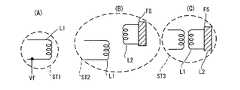
図5(A)〜図5(F)は、1次コイルに2次コイルの磁性体が接近した場合のインダクタンスの増加について説明するための図である。上述のとおり、ここでいう「インダクタンス」は、磁性体付きの2次コイルの接近によって変動するインダクタンス(正確には、見かけ上のインダクタンス)である。「見かけ上のインダクタンス」という用語は、1次コイル単独のインダクタンス(2次コイルの接近の影響を受けないときのインダクタンス)と区別するために使用している。以下の説明では、Lpsと表記されるインダクタンスが、見かけ上のインダクタンスである。 FIGS. 5A to 5F are diagrams for explaining an increase in inductance when the magnetic material of the secondary coil approaches the primary coil. As described above, the “inductance” referred to here is an inductance (to be exact, an apparent inductance) that fluctuates due to the approach of a secondary coil with a magnetic material. The term “apparent inductance” is used to distinguish from the inductance of the primary coil alone (inductance when not affected by the proximity of the secondary coil). In the following description, an inductance represented as Lps is an apparent inductance.
図5(A)に示すように、2次コイルL2には、磁性体(FS)が付属している。図5(B)に示すように、この磁性体(FS)は、例えば、平面コイルである2次コイルL2と回路基板3100間に存在する磁気シールド材としての磁性体である(これに限定されるものではなく、2次コイルL2のコアとしての磁性体であってもよい)。 As shown in FIG. 5A, a magnetic body (FS) is attached to the secondary coil L2. As shown in FIG. 5B, this magnetic body (FS) is, for example, a magnetic body as a magnetic shield material existing between the secondary coil L2 that is a planar coil and the circuit board 3100 (limited to this). It may be a magnetic body as a core of the secondary coil L2 instead of a thing).
図5(C)に示される1次コイルL1単独の等価回路は、図5(D)に示されるようになり、その共振周波数は図示されるようにfpとなる。すなわち、共振周波数は、L1とC1によって決定される。ここで、図5(E)に示すように、2次コイルL2が接近すると、2次コイルL1に付属している磁性体(FS)が1次コイルL1と結合し、図5(F)に示すように、1次コイル(L1)の磁束が磁性体(FS)を通過することになり、磁束密度が増加する。これによって、1次コイルのインダクタンスは上昇する。このときの1次コイルL1の共振周波数は、図示されるようにfscとなる。すなわち、共振周波数は、Lps(2次コイルの接近による影響を考慮した1次コイルの見かけ上のインダクタンス)と1次側のコンデンサC1に依存する。すなわち、1次コイルの見かけ上のインダクタンスLpsは、次のように表すことができる。Lps=L1+ΔL。この式において、L1は、1次コイル単独のインダクタンスであり、ΔLは、1次コイルに磁性体FSが接近したことに起因するインダクタンスの上昇分である。Lpsの具体的な値は、2次コイルが接近したときの1次コイルのインダクタンスを、例えば、計測器で実測することによって取得することができる。 An equivalent circuit of the primary coil L1 alone shown in FIG. 5C is as shown in FIG. 5D, and its resonance frequency is fp as shown. That is, the resonance frequency is determined by L1 and C1. Here, as shown in FIG. 5E, when the secondary coil L2 approaches, the magnetic body (FS) attached to the secondary coil L1 is coupled to the primary coil L1, and FIG. As shown, the magnetic flux of the primary coil (L1) passes through the magnetic body (FS), and the magnetic flux density increases. This increases the inductance of the primary coil. The resonance frequency of the primary coil L1 at this time is fsc as shown in the figure. That is, the resonance frequency depends on Lps (apparent inductance of the primary coil in consideration of the influence of the approach of the secondary coil) and the primary side capacitor C1. That is, the apparent inductance Lps of the primary coil can be expressed as follows. Lps = L1 + ΔL. In this equation, L1 is the inductance of the primary coil alone, and ΔL is the increase in inductance due to the magnetic body FS approaching the primary coil. A specific value of Lps can be acquired by actually measuring the inductance of the primary coil when the secondary coil approaches, for example, by measuring with a measuring instrument.
次に、両コイルの接近によって、1次コイルのインダクタンスがどのように変化するかについて考察する。 Next, consider how the inductance of the primary coil changes due to the approach of both coils.
図6(A)〜図6(D)は、1次コイルと2次コイルの相対的な位置関係の例を示す図である。図中、PA1は、1次コイルL1の中心点を示し、PA2は、2次コイルL2の中心点を示す。 6A to 6D are diagrams illustrating examples of the relative positional relationship between the primary coil and the secondary coil. In the figure, PA1 indicates the center point of the primary coil L1, and PA2 indicates the center point of the secondary coil L2.
図6(A)では、両コイルの位置が遠いため相互の影響はないが、図6(B)のように2次コイル(L2)が1次コイル(L1)に接近すると、図5で説明したように1次コイルのインダクタンスが増大しはじめる。図6(C)では、自己誘導に加えて、両コイルが結合して相互誘導(一方のコイルの磁束を他方のコイルの磁束によって相殺しようとする作用)が働き、そして、図6(D)に示すように、両コイルの位置が完全に一致すると、2次コイル(L2)側に電流が流れるため、相互誘導による磁束の相殺によって洩れ磁束は減少し、コイルのインダクタンスは減少する。すなわち、位置合わせが行われたことによって2次側機器が動作を開始し、その2次側機器の動作開始に伴って2次コイル(L2)に電流が流れ、これによって相互誘導による磁束の相殺が生じ、洩れ磁束が減少して1次コイル(L1)のインダクタンスが減少する。 6A, since the positions of both coils are far from each other, there is no mutual influence. However, when the secondary coil (L2) approaches the primary coil (L1) as shown in FIG. As described above, the inductance of the primary coil starts to increase. In FIG. 6 (C), in addition to self-induction, both coils are coupled to each other (an action of canceling the magnetic flux of one coil by the magnetic flux of the other coil), and FIG. 6 (D) As shown in FIG. 2, when the positions of the two coils are completely coincident with each other, a current flows to the secondary coil (L2) side. Therefore, the leakage flux is reduced by canceling out the magnetic flux by mutual induction, and the inductance of the coil is reduced. That is, when the alignment is performed, the secondary device starts operating, and when the secondary device starts operating, a current flows through the secondary coil (L2), thereby canceling the magnetic flux due to mutual induction. As a result, leakage flux decreases and the inductance of the primary coil (L1) decreases.
図7は、1次コイルと2次コイルの相対距離と、1次コイルのインダクタンスの関係を示す図である。図7において、横軸が相対距離であり、縦軸がインダクタンスである。ここで、「相対距離」とは、「2つのコイルの中心の横方向のずれ量を規格化した相対値」である。なお、相対距離は、両コイルが横方向にどれだけずれているかを示す指標の一つであり、相対距離の代わりに、絶対距離(例えば、両コイルの中心がどれだけずれているかを、ミリメートルで示した絶対値)を使用してもよい。図7において、相対距離がd1のときは、2次コイルの影響がなく、1次コイルL1のインダクタンスは、1次コイル単独のインダクタンス“a”である。2次コイルL2が接近してくると(相対距離d2)、磁性体の影響で磁束密度が増大するためインダクタンス“b”まで上昇する。 FIG. 7 is a diagram illustrating the relationship between the relative distance between the primary coil and the secondary coil and the inductance of the primary coil. In FIG. 7, the horizontal axis represents the relative distance, and the vertical axis represents the inductance. Here, the “relative distance” is “a relative value obtained by standardizing the amount of lateral deviation between the centers of the two coils”. The relative distance is one of the indexes indicating how much the coils are displaced in the lateral direction. Instead of the relative distance, the absolute distance (for example, how much the centers of the coils are displaced is expressed in millimeters). (Absolute value indicated by) may be used. In FIG. 7, when the relative distance is d1, there is no influence of the secondary coil, and the inductance of the primary coil L1 is the inductance “a” of the primary coil alone. When the secondary coil L2 approaches (relative distance d2), the magnetic flux density increases due to the influence of the magnetic material, and thus the inductance rises to the inductance “b”.
さらに2次コイルL2が接近すると(相対距離d3)、インダクタンスは“c”まで上昇する。さらに2次コイルが接近すると(相対距離d4)、インダクタンスは“d”まで上昇する。この状態となるコイル間の結合が生じ、以後は、相互インダクタンスの影響が支配的となる。 When the secondary coil L2 further approaches (relative distance d3), the inductance increases to “c”. When the secondary coil further approaches (relative distance d4), the inductance increases to “d”. Coupling between the coils in this state occurs, and thereafter, the influence of the mutual inductance becomes dominant.
すなわち、相対距離d5では、相互誘導の影響が支配的になるためにインダクタンスは低下して“e”となる。相対距離0(1次コイルと2次コイルの各中心が、XY平面の中心に位置する場合)では、磁束の相殺によって洩れ磁束が最小となり、インダクタンスは一定値(図7の「中心のインダクタンス」)に収束する。 That is, at the relative distance d5, since the influence of mutual induction becomes dominant, the inductance decreases to “e”. At a relative distance of 0 (when the centers of the primary coil and the secondary coil are located at the center of the XY plane), the leakage flux is minimized by canceling out the magnetic flux, and the inductance is a constant value ("center inductance" in FIG. 7). ) To converge.
ここで、相対距離“d2”が送電限界範囲を示し、また、相対距離が“d3”と“d4”で規定される範囲に収まっていれば所望の送電が可能であるとする(つまり、d3とd4で規定される範囲が位置許容範囲LQとする)。この場合、インダクタンスしきい値(INth1)を用いれば、2次コイル(L2)が相対距離d2まで接近したことを検出することができる。同様に、インダクタンスしきい値(INth2)を用いれば、2次コイル(L2)が、相対距離d2とd4で規定される相対距離内にあるか否かを検出することができる。すなわち、インダクタンスの増大に起因する1次コイルのインダクタンスの上昇の程度を調べることによって、1次コイルと2次コイルの相対距離が、位置許容範囲(LQ)内にあるか否かを判定することができる(この場合、相対距離がより小さい範囲での判定はできないが、送電の位置合わせの指標としては、このレベルの判定であれば十分に実用に耐える)。 Here, the relative distance “d2” indicates the power transmission limit range, and if the relative distance is within the range defined by “d3” and “d4”, the desired power transmission is possible (that is, d3 And the range defined by d4 is the position allowable range LQ). In this case, if the inductance threshold value (INth1) is used, it can be detected that the secondary coil (L2) has approached the relative distance d2. Similarly, if the inductance threshold value (INth2) is used, it can be detected whether or not the secondary coil (L2) is within the relative distance defined by the relative distances d2 and d4. That is, it is determined whether or not the relative distance between the primary coil and the secondary coil is within the allowable position range (LQ) by examining the degree of increase in the inductance of the primary coil due to the increase in inductance. (In this case, it is impossible to make a determination in a range where the relative distance is smaller, but this level of determination is sufficiently practical as an index for alignment of power transmission).
例えば、2次コイル(L2)の接近によってインダクタンス値が上昇したことを第1のインダクタンスしきい値(INth1)を用いて検出したとすれば、それは、2次コイルL2が送電可能範囲付近にまで接近してきたことを示している。 For example, if it is detected by using the first inductance threshold value (INth1) that the inductance value has increased due to the approach of the secondary coil (L2), it means that the secondary coil L2 is close to the power transmission possible range. Indicates that you are approaching.
そこで、次に、1次コイルを所定の走査パターンに従って移動(スキャン)させる。これによって、1次コイル(L1)と2次コイル(L2)の相対距離がさらに縮小されれば、インダクタンスはさらに上昇し、やがて、図7のc点まで達する。このことが、第2のインダクタンスしきい値(INth2)によって検出されると、1次コイルの移動(スキャン)を停止する。使用するXYステージの制動の精度にもよるが、これによって、1次コイル(L1)と2次コイル(L2)の相対距離は、ほぼd3〜d5の範囲(位置許容範囲LQ)に収まることになる。 Therefore, next, the primary coil is moved (scanned) in accordance with a predetermined scanning pattern. Accordingly, if the relative distance between the primary coil (L1) and the secondary coil (L2) is further reduced, the inductance further increases and eventually reaches point c in FIG. When this is detected by the second inductance threshold value (INth2), the movement (scanning) of the primary coil is stopped. Depending on the braking accuracy of the XY stage to be used, the relative distance between the primary coil (L1) and the secondary coil (L2) is within the range of d3 to d5 (position allowable range LQ). Become.
実際には、上述のインダクタンスしきい値(INth1,INth2)に対応する電圧しきい値(Vth1,Vth2)を用いて、両コイルの相対位置関係を判定する。以下、具体的に説明する。 Actually, the relative positional relationship between the two coils is determined using voltage threshold values (Vth1, Vth2) corresponding to the above-described inductance threshold values (INth1, INth2). This will be specifically described below.
図8は、インダクタンスの増大によって、1次コイルを含む共振回路の共振周波数の変化を示す図である。2次コイルL2に付属する磁性体(FS)の接近によって1次コイルのインダクタンスが増大すると、図8に示すように、1次コイルを含む共振回路の共振特性はQ1からQ2に変化する。ここで、1次コイルの駆動周波数をfdとすれば、1次コイルL1のインダクタンス値の増大に伴う共振特性のシフトに起因して、コイル端電圧(もしくは電流)がΔAだけ低下することになる。このΔAの変化に着目することによって、コイル端電圧(もしくは電流)に基づく両コイルの相対位置の判定が可能となる。 FIG. 8 is a diagram illustrating a change in the resonance frequency of the resonance circuit including the primary coil due to an increase in inductance. When the inductance of the primary coil increases due to the approach of the magnetic body (FS) attached to the secondary coil L2, the resonance characteristic of the resonance circuit including the primary coil changes from Q1 to Q2, as shown in FIG. Here, if the drive frequency of the primary coil is fd, the coil end voltage (or current) is reduced by ΔA due to the shift of the resonance characteristics accompanying the increase of the inductance value of the primary coil L1. . By paying attention to this change in ΔA, it is possible to determine the relative position of both coils based on the coil end voltage (or current).
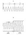
図9(A)〜図9(C)は1次コイルと2次コイルの相対位置の変化例を示す図である。図10は、1次コイルと2次コイルの位置関係を自動的に調整する方法を説明するための図である。 FIG. 9A to FIG. 9C are diagrams illustrating examples of changes in the relative positions of the primary coil and the secondary coil. FIG. 10 is a diagram for explaining a method of automatically adjusting the positional relationship between the primary coil and the secondary coil.
送電制御装置20(図2参照)は、図10の期間T1,期間T2に示すように、所定周期で間欠的に1次コイルL1を、周波数fdで駆動する。そして、図9に示されるようにコイル端電圧Vf(あるいはコイル電流)を観測する。図9(A)のように2次コイルL2がないときは、図10の期間T1,T2に示すように、コイル端電圧(交流)の振幅
Vfは、vth1を下回ることはない。The power transmission control device 20 (see FIG. 2) intermittently drives the primary coil L1 at the frequency fd at a predetermined cycle as shown in the period T1 and the period T2 in FIG. Then, as shown in FIG. 9, the coil end voltage Vf (or coil current) is observed. When there is no secondary coil L2 as shown in FIG. 9A, the amplitude Vf of the coil end voltage (alternating current) does not fall below vth1, as shown in the periods T1 and T2 of FIG.
図10の時刻t4における駆動では、コイル端電圧Vfは、第1の電圧しきい値Vth1を下回る。これによって、送電制御装置20は、2次コイルL2の接近を検出することができる。この場合、送電制御装置20は、続いて1次コイル(L1)のスキャンを行いながらコイル端電圧Vfの変化を連続的に監視し、両コイルの相対位置のサーチを行う必要がある。よって、送電制御装置20は、時刻t4以降、間欠送電を連続送電に切り換える。この連続送電は、1次コイルL1の移動(スキャン)期間T3は継続される。 In driving at time t4 in FIG. 10, the coil end voltage Vf is lower than the first voltage threshold value Vth1. Thereby, the power
1次コイルL1の移動によって、2次コイルとの距離が縮小され、位置許容範囲LQ(図7参照)内になったときは、コイル端電圧Vfは、第2の電圧しきい値Vth2を下回る。これによって、1次コイルL1の移動(スキャン)が停止されると共に、1次コイルL1の連続駆動も停止される。このようにして、2次コイルL2(磁性体FS)の接近検出ならびに1次コイルL1の位置調整が自動的になされる。 When the distance from the secondary coil is reduced by the movement of the primary coil L1 and is within the position allowable range LQ (see FIG. 7), the coil end voltage Vf is lower than the second voltage threshold Vth2. . Accordingly, the movement (scanning) of the primary coil L1 is stopped and the continuous driving of the primary coil L1 is also stopped. In this way, the proximity detection of the secondary coil L2 (magnetic body FS) and the position adjustment of the primary coil L1 are automatically performed.
より具体的には、図11(A),図11(B)に示されるような動作が行われる。図11(A),図11(B)は、1次コイルと2次コイルの位置関係を自動的に調整するための具体的な回路動作を示す図である。図11(A)に示すように、コイル端電圧Vfが波形モニタ回路14内の抵抗RA1,RA2によって分圧され、ピークホールド回路28によってピーク電圧Vpが検出され、そのピーク電圧Vpが、比較器25内の第1および第2のコンパレータCP1,CP2によって、第1および第2の電圧しきい値(Vth1,Vth2)と比較される。 More specifically, the operation as shown in FIGS. 11A and 11B is performed. FIGS. 11A and 11B are diagrams illustrating specific circuit operations for automatically adjusting the positional relationship between the primary coil and the secondary coil. As shown in FIG. 11A, the coil end voltage Vf is divided by resistors RA1 and RA2 in the
1次コイル位置制御回路31は、第1のコンパレータCP1の出力信号(相対位置信号)PE1がハイレベルからローレベルに変化すると(図11(B)の時刻t10)、アクチュエータ制御回路27に指示して1次コイル(L1)の移動を開始させ、かつ、上述のとおり、間欠駆動を連続駆動に切り換える。 When the output signal (relative position signal) PE1 of the first comparator CP1 changes from the high level to the low level (time t10 in FIG. 11B), the primary coil
その後、第2のコンパレータCP2の出力信号(相対位置信号)PE2がハイレベルからローレベルに変化すると(図11(B)の時刻t11)、アクチュエータ制御回路27に指示して1次コイル(L1)の移動を停止させると共に、1次コイルの駆動を停止させる。 Thereafter, when the output signal (relative position signal) PE2 of the second comparator CP2 changes from the high level to the low level (time t11 in FIG. 11B), the
図12(A),図12(B)は、1次コイルの移動(スキャン)について説明するための図である。図12(A)に示すように、送電装置(送電モジュール)10は、1次コイルL1を備える。1次コイルL1の位置を移動させるときは、アクチュエータを用いて、下地のXYステージ702をX方向またはY方向に移動させる。なお、図12(A)において、PA1は、1次コイルL1の中心を示す。
図12(B)に示すように、1次コイルL1の位置調整のための走査は、例えば、螺旋状のパターンで行われる。螺旋状スキャンによれば、1次コイル位置を、高精度に広範囲にわたって移動させることができる(但し、これに限定されるものではない)。12A and 12B are diagrams for explaining the movement (scanning) of the primary coil. As shown in FIG. 12A, the power transmission device (power transmission module) 10 includes a primary coil L1. When the position of the primary coil L1 is moved, the
As shown in FIG. 12B, scanning for position adjustment of the primary coil L1 is performed, for example, in a spiral pattern. According to the helical scan, the primary coil position can be moved over a wide range with high accuracy (however, the present invention is not limited to this).
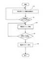
以上説明した、1次コイルの自動的な位置調整の手順を示すと、図13のようになる。図13は、1次コイルの自動的な位置調整の手順を示すフロー図である。 The procedure for automatic position adjustment of the primary coil described above is shown in FIG. FIG. 13 is a flowchart showing a procedure for automatic position adjustment of the primary coil.
図示されるように、2次コイルの接近を検出するために、1次コイルの間欠的な駆動(周波数fd)を行い(ステップS1)、Vth1を用いた判定によって2次コイル接近が検出されると(ステップS2)、連続駆動に切り換えると共に螺旋状スキャンを開始する(ステップS3)。 As shown in the drawing, in order to detect the approach of the secondary coil, the primary coil is intermittently driven (frequency fd) (step S1), and the approach of the secondary coil is detected by the determination using Vth1. (Step S2), switching to continuous driving and starting a helical scan (Step S3).
続いて、Vth2による判定によって両コイルの相対位置が許容範囲内であると判定されると(ステップS4)、連続駆動を停止すると共に螺旋状スキャンを停止する(ステップS5)。 Subsequently, when it is determined by the determination by Vth2 that the relative position of both coils is within the allowable range (step S4), the continuous drive is stopped and the helical scan is stopped (step S5).
(XYステージの構成例と動作)
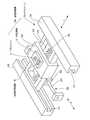
次に、XYステージの構成例と動作について説明する。図14は、XYステージの基本構成を示す斜視図である。(Configuration example and operation of XY stage)
Next, a configuration example and operation of the XY stage will be described. FIG. 14 is a perspective view showing the basic configuration of the XY stage.
図示されるように、XYステージ702は、一対のガイドレール100と、X軸スライダ200と、Y軸スライダ300と、を有する。これらに使用する材料は、例えば、アルミニウム、鉄、グラナイト(御影石)、セラミックス等である。 As illustrated, the
一対のガイドレール100は互いに対向するガイド溝110を持ち、X軸方向に延在して平行に設けられる。一対のガイドレール100は図示しない定盤に固定される。 The pair of
一対のガイドレール100の間にX軸スライダ200が係合される。X軸スライダ200は矩形平板状をしており、その両端部がそれぞれ対向するガイド溝110に嵌め込まれて係合され、ガイド溝110に沿ってX軸方向の移動は許容されるが、Y軸方向の動きは規制されるようになっている。したがってX軸スライダ200は一対のガイドレール100に沿ってX軸方向に往復運動できる。 The
なお、ガイドレール100に設けたガイド溝110をX軸スライダ200側に設け、ガイドレール100側にX軸スライダ200に設けたガイド溝に嵌まる凸条を設けるようにしてもよい。ガイドレール100とX軸スライダ200との係合部は、3つの面で支持されていればよく、ガイド溝の形状は問わない。 Note that the
X軸スライダ200を囲むようにY軸スライダ300が装着されている。Y軸スライダ300は、矩形平板状のX軸スライダ200の断面形状に合致するように、断面略コ字型をしている。その略コ字型をしたY軸スライダ300の開口部が内側に折り返されている。なお、Y軸スライダ300は上部が開口していてもよく、さらには全く開口していない断面略ロ字型をしたものでもよい。 A Y-
これによりガイド溝110に係合するX軸スライダ200の幅方向の両端部は、Y軸スライダ300によって上面、側面、下面の3面が支持される。そしてY軸スライダ300はX軸スライダ200に装着されることにより、X軸スライダ200に対してX軸方向の動きが規制されて、X軸スライダ200がX軸方向に移動するとそれに伴ってX軸方向に移動する。また、X軸スライダ200に対してY軸方向の動きが許容されて、X軸スライダ200に対してY軸方向に移動できるようになっている。X軸スライダ200はスライドするだけでなく、X軸スライダ200に対してY軸スライダ300をY軸方向に移動させるガイドも兼ねている。また、Y軸スライダ300の上部が、XY軸運動をさせる対象を載せるトッププレート(可動主面)となる。 As a result, the Y-
図示されるように、トッププートとしてのY軸スライダ300の主面には、1次コイル(円形の巻線コイル)L1と、IC化された送電制御装置20と、を含む送電装置10が搭載されている。 As shown in the drawing, a
また、図14のXYステージ702では、駆動源として、高精度なリニアモータを使用している。なおリニアモータに代えてボールネジ機構としてもよい。 In the
X軸スライダ200を移動させるX軸リニアモータ600は一対のガイドレール100間に設けてある。ロッド状の固定子610に装着されたX軸リニアモータ600の可動子620をX軸スライダ200の下部に固着することで、X軸スライダ200を往復動自在としている。 An X-axis
また、Y軸スライダ300は、Y軸リニアモータ700によって往復駆動される。X軸スライダ200に凹部210が設けられ、その凹部210に、Y軸リニアモータ700が収納されている。これによって、ステージ高を抑えることができる。 The Y-
X軸リニアモータ600およびY軸リニアモータ700は各々、図2に示されるX方向アクチュエータ720およびY方向アクチュエータ730に相当する。 The X-axis
このようなXYステージ702に、1次コイル(円形の巻線コイル)L1およびIC化された送電制御装置20を含む送電装置10が搭載されることによって、送電側装置(無接点電力伝送システムの送電機構)704が構成される。 By mounting the
そして、図1(B)に示したように、送電側装置704は、プレーンな平面をもつ構造物(例えば、机等)の内部に埋め込まれる。これによって、概略な位置に置かれた2次側機器(携帯端末等)の2次コイル位置に対応するように、1次コイルのXY平面における位置を自動的に移動させることが可能な、次世代の無接点電力伝送システムに対応した送電側装置704が実現される。 Then, as illustrated in FIG. 1B, the power
上述のとおり、本発明の送電制御装置20は、間欠的に1次コイルを駆動し、1次コンダクタンスの上昇によるコイル端電圧(電流)の減少が生じているか否かを常に監視する。そして、2次側機器の接近(2次側機器が所定エリアZ1内に載置されたこと)が検出されれば、1次コイル位置制御回路31による1次コイル位置の自動調整がなされる。したがって、2次側機器の接近検出ならびに1次コイルの位置調整が自動的に行われることになり、ユーザの手間は一切、生じない。 As described above, the power
以上、本発明を、実施形態を参照して説明したが、本発明はこれに限定されるものではなく、種々、変形、応用が可能である。すなわち、本発明の要旨を逸脱しない範囲において多くの変形が可能であることは当業者には容易に理解できるであろう。 The present invention has been described above with reference to the embodiment. However, the present invention is not limited to this, and various modifications and applications are possible. That is, it will be readily understood by those skilled in the art that many modifications are possible without departing from the scope of the present invention.
従って、このような変形例はすべて本発明の範囲に含まれるものとする。例えば、明細書又は図面において、少なくとも一度、より広義または同義な異なる用語(低電位側電源、電子機器等)と共に記載された用語(GND、携帯電話機・充電器等)は、明細書又は図面のいかなる箇所においても、その異なる用語に置き換えることができる。また本実施形態および変形例の全ての組み合わせも、本発明の範囲に含まれる。 Accordingly, all such modifications are intended to be included in the scope of the present invention. For example, in the specification or the drawings, terms (GND, mobile phone / charger, etc.) described together with different terms having a broader meaning or the same meaning (low-potential side power supply, electronic device, etc.) at least once in the specification or the drawings It can be replaced by the different terms at any point. All combinations of the present embodiment and the modified examples are also included in the scope of the present invention.
また、送電制御装置、送電装置、受電制御装置、受電装置の構成ならびに動作や、1次側における2次側の負荷検出の手法も、本実施形態で説明したものに限定されず、種々の変形実施が可能である。 Further, the configuration and operation of the power transmission control device, the power transmission device, the power reception control device, and the power reception device, and the method of detecting the load on the secondary side on the primary side are not limited to those described in the present embodiment, and various modifications are possible. Implementation is possible.
本発明の少なくとも一つの実施態様によれば、例えば、以下の効果が得られる。但し、以下の効果は同時に得られるとは限らず、以下の効果の列挙が本発明を不当に限定する根拠として用いられてはならない。
(1)2次側機器が概略の位置に置かれたとしても、1次コイルが自動的に最適位置に移動するため、常に適正な送電が実現される。
(2)2次側機器の大きさ、形状、機器デザイン等に影響されず、常に適正な送電が実現されるため、無接点電力伝送システムの汎用性が格段に向上する。
(3)2次側機器の設計の自由度は何ら制限されないため、2次側機器のメーカの負担が生じない。
(4)特別な回路(位置検出素子等)を用いず、無接点電力伝送システムに備わっている回路構成を活用してコイル間の相対的な位置関係を検出するため、構成が複雑化せず、かつ実現が容易である。
(5)例えば、フラットな平面をもつ構造物(例えば机)の所定エリア上に携帯端末等を載置するだけで、自動的に一次コイルの位置調整がなされて充電等が可能となる、極めて汎用性および利便性の高い次世代の無接点電力伝送システムを実現することができる。According to at least one embodiment of the present invention, for example, the following effects can be obtained. However, the following effects are not always obtained, and the enumeration of the following effects should not be used as a basis for unduly limiting the present invention.
(1) Even if the secondary device is placed at the approximate position, the primary coil automatically moves to the optimum position, so that proper power transmission is always realized.
(2) Appropriate power transmission is always achieved without being affected by the size, shape, device design, etc. of the secondary side device, so the versatility of the non-contact power transmission system is greatly improved.
(3) Since the degree of freedom in designing the secondary device is not limited, the burden on the manufacturer of the secondary device does not occur.
(4) Since the relative positional relationship between the coils is detected by utilizing the circuit configuration provided in the non-contact power transmission system without using a special circuit (position detection element or the like), the configuration is not complicated. And easy to implement.
(5) For example, by simply placing a mobile terminal or the like on a predetermined area of a structure having a flat plane (for example, a desk), the position of the primary coil is automatically adjusted to enable charging, etc. A next-generation contactless power transmission system with high versatility and convenience can be realized.
本発明は、汎用性および利便性が格段に向上した次世代の無接点電力伝送システムを提供するという効果を奏し、したがって、特に、送電制御装置(送電制御IC)、送電装置(ICモジュール等)、送電側装置(送電装置、アクチュエータならびにXYステージを備えた1次側構造体)、無接点電力伝送システムとして有用である。 The present invention has the effect of providing a next-generation contactless power transmission system with greatly improved versatility and convenience, and therefore, in particular, a power transmission control device (power transmission control IC), a power transmission device (IC module, etc.). It is useful as a power transmission side device (a primary side structure including a power transmission device, an actuator, and an XY stage) and a non-contact power transmission system.
L1 1次コイル、L2 2次コイル、10 送電装置、12 送電部、
14 波形モニタ回路、16 表示部、20 送電制御装置、22 送電側制御回路、
23 駆動クロック生成回路、24 発振回路、25 比較器、
26 ドライバ制御回路、27 アクチュエータ制御回路、28 波形検出回路、
29 相対位置信号生成回路、31 1次コイル位置制御回路、40 受電装置、
42 受電部、43 整流回路、46 負荷変調部、48 給電制御部、
50 受電制御装置、52 受電側制御回路、56 位置検出回路、58 発振回路、
60 周波数検出回路、62 満充電検出回路、90 2次側機器の負荷、
92 充電制御装置、94 バッテリ(2次電池)、
702 XYテーブル 704 送電側装置(1次側構造体)、
710 アクチュエータドライバ、720 X方向アクチュエータ、
730 Y方向アクチュエータ、PE(PE1,PE2) 相対位置信号L1 primary coil, L2 secondary coil, 10 power transmission device, 12 power transmission unit,
14 waveform monitor circuit, 16 display unit, 20 power transmission control device, 22 power transmission side control circuit,
23 drive clock generation circuit, 24 oscillation circuit, 25 comparator,
26 Driver control circuit, 27 Actuator control circuit, 28 Waveform detection circuit,
29 Relative position signal generation circuit, 31 Primary coil position control circuit, 40 Power receiving device,
42 power receiving unit, 43 rectifier circuit, 46 load modulation unit, 48 power feeding control unit,
50 power reception control device, 52 power reception side control circuit, 56 position detection circuit, 58 oscillation circuit,
60 frequency detection circuit, 62 full charge detection circuit, 90 secondary side equipment load,
92 charge control device, 94 battery (secondary battery),
702 XY table 704 power transmission side device (primary side structure),
710 Actuator driver, 720 X direction actuator,
730 Y direction actuator, PE (PE1, PE2) Relative position signal
Claims (7)
Translated fromJapanese前記受電装置への送電を制御する送電側制御回路と、
前記1次コイルのXY平面上における位置を移動させるためのアクチュエータの動作を制御するアクチュエータ制御回路と、
前記1次コイルのコイル端電圧またはコイル電流に基づいて、前記1次コイルと前記2次コイルの相対位置検出信号を生成する相対位置検出信号生成回路と、
前記相対位置検出信号が示す前記1次コイルと前記2次コイルの相対位置が許容範囲になるように、前記アクチュエータ制御回路に指示して前記1次コイルのXY平面上における位置を移動させる1次コイル位置制御回路と、
を有することを特徴とする送電制御装置。A power transmission control device provided in the power transmission device in a non-contact power transmission system for transmitting power from a power transmission device to a power reception device in a contactless manner via an electromagnetically coupled primary coil and secondary coil. ,
A power transmission side control circuit for controlling power transmission to the power receiving device;
An actuator control circuit for controlling the operation of the actuator for moving the position of the primary coil on the XY plane;
A relative position detection signal generation circuit that generates a relative position detection signal of the primary coil and the secondary coil based on a coil end voltage or a coil current of the primary coil;
A primary that moves the position of the primary coil on the XY plane by instructing the actuator control circuit so that the relative position of the primary coil and the secondary coil indicated by the relative position detection signal falls within an allowable range. A coil position control circuit;
A power transmission control device comprising:
前記2次コイルは磁性体付きの2次コイルであり、
前記1次コイル位置制御回路は、
前記磁性体付きの2次コイルの接近によって、前記1次コイルのインダクタンスが増大し、前記1次コイルを所定周波数で駆動した場合のコイル端電圧もしくはコイル電流が減少して第1のしきい値に達すると、前記アクチュエータ制御回路に指示して、前記1次コイルのXY平面上における位置を所定の走査パターンに従って移動させる、
ことを特徴とする送電制御装置。The power transmission control device according to claim 1,
The secondary coil is a secondary coil with a magnetic material,
The primary coil position control circuit includes:
Due to the approach of the secondary coil with the magnetic material, the inductance of the primary coil increases, and the coil end voltage or coil current when the primary coil is driven at a predetermined frequency decreases, and the first threshold value is reached. The actuator control circuit is instructed to move the position of the primary coil on the XY plane according to a predetermined scanning pattern,
A power transmission control device.
前記1次コイル位置制御回路は、
前記1次コイルの位置の移動によって、前記コイル端電圧もしくはコイル電流がさらに減少して第2のしきい値に達すると、前記1次コイルの移動を停止する、
ことを特徴とする送電制御装置。A power transmission control device according to claim 2,
The primary coil position control circuit includes:
When the coil end voltage or coil current is further reduced by the movement of the position of the primary coil and reaches the second threshold value, the movement of the primary coil is stopped.
A power transmission control device.
前記送電側制御回路は、
前記2次コイルの接近を検出するために、所定周波数の駆動信号によって前記1次コイルを間欠的に駆動させると共に、前記1次コイルの走査の実行期間においては前記1次コイルを連続的に駆動する、
ことを特徴とする送電制御装置。A power transmission control device according to claim 2,
The power transmission side control circuit is:
In order to detect the approach of the secondary coil, the primary coil is intermittently driven by a drive signal of a predetermined frequency, and the primary coil is continuously driven during the scanning period of the primary coil. To
A power transmission control device.
前記1次コイルと、
を有することを特徴とする送電装置。The power transmission control device according to any one of claims 1 to 4,
The primary coil;
A power transmission device comprising:
請求項5記載の送電装置と、
前記アクチュエータ制御回路によって動作が制御されるアクチュエータと、
前記アクチュエータによって駆動される、前記1次コイルを搭載したXYステージと、
を有することを特徴とする送電側装置。A power transmission side device in a non-contact power transmission system,
A power transmission device according to claim 5;
An actuator whose operation is controlled by the actuator control circuit;
An XY stage mounted with the primary coil driven by the actuator;
A power transmission side device characterized by comprising:
前記送電側装置の前記送電装置からの電力伝送を受ける、前記2次コイルを有する受電装置と、
を有することを特徴とする無接点電力伝送システム。A power transmission side device according to claim 6;
A power receiving device having the secondary coil for receiving power transmission from the power transmission device of the power transmission side device;
A non-contact power transmission system comprising:
Priority Applications (3)
| Application Number | Priority Date | Filing Date | Title |
|---|---|---|---|
| JP2007249375AJP2009081943A (en) | 2007-09-26 | 2007-09-26 | Power transmission control device, power transmission device, power transmission side device, and non-contact power transmission system |
| EP08016823AEP2043226A3 (en) | 2007-09-26 | 2008-09-25 | Power transmission control device, power transmitting device, power-transmitting-side device, and non-contact power transmission system |
| US12/237,733US20090079387A1 (en) | 2007-09-26 | 2008-09-25 | Power transmission control device, power transmitting device, power-transmitting-side device, and non-contact power transmission system |
Applications Claiming Priority (1)
| Application Number | Priority Date | Filing Date | Title |
|---|---|---|---|
| JP2007249375AJP2009081943A (en) | 2007-09-26 | 2007-09-26 | Power transmission control device, power transmission device, power transmission side device, and non-contact power transmission system |
Publications (1)
| Publication Number | Publication Date |
|---|---|
| JP2009081943Atrue JP2009081943A (en) | 2009-04-16 |
Family
ID=40056193
Family Applications (1)
| Application Number | Title | Priority Date | Filing Date |
|---|---|---|---|
| JP2007249375AWithdrawnJP2009081943A (en) | 2007-09-26 | 2007-09-26 | Power transmission control device, power transmission device, power transmission side device, and non-contact power transmission system |
Country Status (3)
| Country | Link |
|---|---|
| US (1) | US20090079387A1 (en) |
| EP (1) | EP2043226A3 (en) |
| JP (1) | JP2009081943A (en) |
Cited By (4)
| Publication number | Priority date | Publication date | Assignee | Title |
|---|---|---|---|---|
| JP2012514967A (en)* | 2009-01-06 | 2012-06-28 | アクセス ビジネス グループ インターナショナル リミテッド ライアビリティ カンパニー | Contactless power supply |
| JP2021502793A (en)* | 2017-11-13 | 2021-01-28 | ティーディーケイ・エレクトロニクス・アクチェンゲゼルシャフトTdk Electronics Ag | Dynamic transmission coil positioning system, wireless power transmission system and transmission coil positioning method |
| JP6906712B1 (en)* | 2020-04-22 | 2021-07-21 | 三菱電機株式会社 | Power transmission equipment and wireless power transmission system |
| JP2023129014A (en)* | 2022-03-04 | 2023-09-14 | トヨタ自動車株式会社 | Vehicle and vehicle control method |
Families Citing this family (142)
| Publication number | Priority date | Publication date | Assignee | Title |
|---|---|---|---|---|
| CN101802942A (en) | 2007-01-29 | 2010-08-11 | 普迈公司 | Pinless power coupling |
| EP3975372B1 (en) | 2007-03-22 | 2024-01-31 | Powermat Technologies Ltd. | Efficiency monitor for inductive power transmission |
| US9421388B2 (en) | 2007-06-01 | 2016-08-23 | Witricity Corporation | Power generation for implantable devices |
| US8115448B2 (en) | 2007-06-01 | 2012-02-14 | Michael Sasha John | Systems and methods for wireless power |
| US10068701B2 (en) | 2007-09-25 | 2018-09-04 | Powermat Technologies Ltd. | Adjustable inductive power transmission platform |
| KR20100061845A (en) | 2007-09-25 | 2010-06-09 | 파우워매트 엘티디. | Adjustable inductive power transmission platform |
| US8193769B2 (en) | 2007-10-18 | 2012-06-05 | Powermat Technologies, Ltd | Inductively chargeable audio devices |
| US8536737B2 (en) | 2007-11-19 | 2013-09-17 | Powermat Technologies, Ltd. | System for inductive power provision in wet environments |
| US20100219183A1 (en) | 2007-11-19 | 2010-09-02 | Powermat Ltd. | System for inductive power provision within a bounding surface |
| US8421407B2 (en)* | 2008-02-25 | 2013-04-16 | L & P Property Management Company | Inductively coupled work surfaces |
| US8228026B2 (en)* | 2008-02-25 | 2012-07-24 | L & P Property Management Company | Inductively coupled shelving and storage containers |
| CN102084442B (en) | 2008-03-17 | 2013-12-04 | 鲍尔马特技术有限公司 | Inductive transmission system |
| US9337902B2 (en) | 2008-03-17 | 2016-05-10 | Powermat Technologies Ltd. | System and method for providing wireless power transfer functionality to an electrical device |
| US9331750B2 (en) | 2008-03-17 | 2016-05-03 | Powermat Technologies Ltd. | Wireless power receiver and host control interface thereof |
| US9960642B2 (en) | 2008-03-17 | 2018-05-01 | Powermat Technologies Ltd. | Embedded interface for wireless power transfer to electrical devices |
| US9960640B2 (en) | 2008-03-17 | 2018-05-01 | Powermat Technologies Ltd. | System and method for regulating inductive power transmission |
| US8320143B2 (en) | 2008-04-15 | 2012-11-27 | Powermat Technologies, Ltd. | Bridge synchronous rectifier |
| AU2009254785A1 (en) | 2008-06-02 | 2009-12-10 | Powermat Technologies Ltd. | Appliance mounted power outlets |
| US11979201B2 (en) | 2008-07-02 | 2024-05-07 | Powermat Technologies Ltd. | System and method for coded communication signals regulating inductive power transmissions |
| US8188619B2 (en) | 2008-07-02 | 2012-05-29 | Powermat Technologies Ltd | Non resonant inductive power transmission system and method |
| US8981598B2 (en) | 2008-07-02 | 2015-03-17 | Powermat Technologies Ltd. | Energy efficient inductive power transmission system and method |
| WO2010004560A1 (en) | 2008-07-08 | 2010-01-14 | Powermat Ltd. | Display device |
| US9090170B2 (en)* | 2008-08-26 | 2015-07-28 | Alex Mashinsky | Self-charging electric vehicle and aircraft and wireless energy distribution system |
| EP2342797A2 (en) | 2008-09-23 | 2011-07-13 | Powermat Ltd | Combined antenna and inductive power receiver |
| US8922066B2 (en) | 2008-09-27 | 2014-12-30 | Witricity Corporation | Wireless energy transfer with multi resonator arrays for vehicle applications |
| US9065423B2 (en) | 2008-09-27 | 2015-06-23 | Witricity Corporation | Wireless energy distribution system |
| US8937408B2 (en) | 2008-09-27 | 2015-01-20 | Witricity Corporation | Wireless energy transfer for medical applications |
| US9184595B2 (en) | 2008-09-27 | 2015-11-10 | Witricity Corporation | Wireless energy transfer in lossy environments |
| US9515494B2 (en) | 2008-09-27 | 2016-12-06 | Witricity Corporation | Wireless power system including impedance matching network |
| US8598743B2 (en) | 2008-09-27 | 2013-12-03 | Witricity Corporation | Resonator arrays for wireless energy transfer |
| US9093853B2 (en) | 2008-09-27 | 2015-07-28 | Witricity Corporation | Flexible resonator attachment |
| US9601266B2 (en) | 2008-09-27 | 2017-03-21 | Witricity Corporation | Multiple connected resonators with a single electronic circuit |
| US9318922B2 (en) | 2008-09-27 | 2016-04-19 | Witricity Corporation | Mechanically removable wireless power vehicle seat assembly |
| US8957549B2 (en) | 2008-09-27 | 2015-02-17 | Witricity Corporation | Tunable wireless energy transfer for in-vehicle applications |
| US9744858B2 (en) | 2008-09-27 | 2017-08-29 | Witricity Corporation | System for wireless energy distribution in a vehicle |
| US8901778B2 (en) | 2008-09-27 | 2014-12-02 | Witricity Corporation | Wireless energy transfer with variable size resonators for implanted medical devices |
| US9160203B2 (en) | 2008-09-27 | 2015-10-13 | Witricity Corporation | Wireless powered television |
| US9105959B2 (en) | 2008-09-27 | 2015-08-11 | Witricity Corporation | Resonator enclosure |
| US8928276B2 (en) | 2008-09-27 | 2015-01-06 | Witricity Corporation | Integrated repeaters for cell phone applications |
| US8643326B2 (en) | 2008-09-27 | 2014-02-04 | Witricity Corporation | Tunable wireless energy transfer systems |
| US9106203B2 (en) | 2008-09-27 | 2015-08-11 | Witricity Corporation | Secure wireless energy transfer in medical applications |
| US8963488B2 (en) | 2008-09-27 | 2015-02-24 | Witricity Corporation | Position insensitive wireless charging |
| US9544683B2 (en) | 2008-09-27 | 2017-01-10 | Witricity Corporation | Wirelessly powered audio devices |
| US8497601B2 (en) | 2008-09-27 | 2013-07-30 | Witricity Corporation | Wireless energy transfer converters |
| US8723366B2 (en)* | 2008-09-27 | 2014-05-13 | Witricity Corporation | Wireless energy transfer resonator enclosures |
| US9246336B2 (en) | 2008-09-27 | 2016-01-26 | Witricity Corporation | Resonator optimizations for wireless energy transfer |
| US20100259110A1 (en)* | 2008-09-27 | 2010-10-14 | Kurs Andre B | Resonator optimizations for wireless energy transfer |
| US8947186B2 (en) | 2008-09-27 | 2015-02-03 | Witricity Corporation | Wireless energy transfer resonator thermal management |
| US8692412B2 (en)* | 2008-09-27 | 2014-04-08 | Witricity Corporation | Temperature compensation in a wireless transfer system |
| US9601261B2 (en) | 2008-09-27 | 2017-03-21 | Witricity Corporation | Wireless energy transfer using repeater resonators |
| US8946938B2 (en) | 2008-09-27 | 2015-02-03 | Witricity Corporation | Safety systems for wireless energy transfer in vehicle applications |
| US8482158B2 (en) | 2008-09-27 | 2013-07-09 | Witricity Corporation | Wireless energy transfer using variable size resonators and system monitoring |
| US8912687B2 (en) | 2008-09-27 | 2014-12-16 | Witricity Corporation | Secure wireless energy transfer for vehicle applications |
| US8772973B2 (en) | 2008-09-27 | 2014-07-08 | Witricity Corporation | Integrated resonator-shield structures |
| US9396867B2 (en) | 2008-09-27 | 2016-07-19 | Witricity Corporation | Integrated resonator-shield structures |
| US8933594B2 (en) | 2008-09-27 | 2015-01-13 | Witricity Corporation | Wireless energy transfer for vehicles |
| US8901779B2 (en) | 2008-09-27 | 2014-12-02 | Witricity Corporation | Wireless energy transfer with resonator arrays for medical applications |
| US20110043049A1 (en)* | 2008-09-27 | 2011-02-24 | Aristeidis Karalis | Wireless energy transfer with high-q resonators using field shaping to improve k |
| US8907531B2 (en) | 2008-09-27 | 2014-12-09 | Witricity Corporation | Wireless energy transfer with variable size resonators for medical applications |
| US9577436B2 (en) | 2008-09-27 | 2017-02-21 | Witricity Corporation | Wireless energy transfer for implantable devices |
| US9035499B2 (en) | 2008-09-27 | 2015-05-19 | Witricity Corporation | Wireless energy transfer for photovoltaic panels |
| US20120086284A1 (en)* | 2008-09-27 | 2012-04-12 | Capanella Andrew J | Wireless transmission of solar generated power |
| US9601270B2 (en) | 2008-09-27 | 2017-03-21 | Witricity Corporation | Low AC resistance conductor designs |
| US20100277121A1 (en)* | 2008-09-27 | 2010-11-04 | Hall Katherine L | Wireless energy transfer between a source and a vehicle |
| US8669676B2 (en) | 2008-09-27 | 2014-03-11 | Witricity Corporation | Wireless energy transfer across variable distances using field shaping with magnetic materials to improve the coupling factor |
| KR20100074595A (en)* | 2008-12-24 | 2010-07-02 | 삼성전자주식회사 | Method and system for wireless charge |
| US8310200B2 (en)* | 2009-04-15 | 2012-11-13 | GM Global Technology Operations LLC | Inductive chargers and inductive charging systems for portable electronic devices |
| JP5340017B2 (en)* | 2009-04-28 | 2013-11-13 | 三洋電機株式会社 | Built-in battery and charging stand |
| DE112010002338T5 (en)* | 2009-06-25 | 2012-08-02 | Tanashin Denki Co., Ltd. | Two-dimensional displacement device |
| RU2548367C2 (en)* | 2009-07-13 | 2015-04-20 | Конинклейке Филипс Электроникс Н.В. | Energy inductive transmission |
| US8482160B2 (en)* | 2009-09-16 | 2013-07-09 | L & P Property Management Company | Inductively coupled power module and circuit |
| KR20110034773A (en)* | 2009-09-29 | 2011-04-06 | 삼성전자주식회사 | Wireless Charger Using Inductive Coupling |
| KR20110050831A (en)* | 2009-11-09 | 2011-05-17 | 삼성전자주식회사 | Apparatus and method for supporting contactless charging in battery charging systems |
| EP2519424A2 (en) | 2009-12-28 | 2012-11-07 | Toyoda Gosei Co., Ltd. | Recharging or connection tray for portable electronic devices |
| JP5539069B2 (en)* | 2010-06-30 | 2014-07-02 | キヤノン株式会社 | Power supply device |
| US8853890B2 (en) | 2010-07-09 | 2014-10-07 | Sony Corporation | Power supply device, communication terminal device, and non-contact power transmission method |
| US9602168B2 (en) | 2010-08-31 | 2017-03-21 | Witricity Corporation | Communication in wireless energy transfer systems |
| KR101830649B1 (en)* | 2010-09-10 | 2018-02-23 | 삼성전자주식회사 | Wireless power supply apparatus, wireless charging apparatus and wireless charging system using the same |
| JP5625723B2 (en)* | 2010-10-15 | 2014-11-19 | ソニー株式会社 | Electronic device, power supply method and power supply system |
| KR101896921B1 (en)* | 2011-05-17 | 2018-09-12 | 삼성전자주식회사 | Wireless power receiver and method for controlling thereof |
| JP5793963B2 (en)* | 2011-05-27 | 2015-10-14 | 日産自動車株式会社 | Non-contact power feeding device |
| US9948145B2 (en) | 2011-07-08 | 2018-04-17 | Witricity Corporation | Wireless power transfer for a seat-vest-helmet system |
| CN108110907B (en) | 2011-08-04 | 2022-08-02 | 韦特里西提公司 | Tunable wireless power supply architecture |
| EP2754222B1 (en) | 2011-09-09 | 2015-11-18 | Witricity Corporation | Foreign object detection in wireless energy transfer systems |
| US20130062966A1 (en) | 2011-09-12 | 2013-03-14 | Witricity Corporation | Reconfigurable control architectures and algorithms for electric vehicle wireless energy transfer systems |
| US9318257B2 (en) | 2011-10-18 | 2016-04-19 | Witricity Corporation | Wireless energy transfer for packaging |
| CA2853824A1 (en) | 2011-11-04 | 2013-05-10 | Witricity Corporation | Wireless energy transfer modeling tool |
| JP2015508987A (en) | 2012-01-26 | 2015-03-23 | ワイトリシティ コーポレーションWitricity Corporation | Wireless energy transmission with reduced field |
| US9184619B2 (en)* | 2012-03-13 | 2015-11-10 | Nokia Technologies Oy | Accessory speaker with wireless charger for mobile device |
| GB2500783A (en)* | 2012-03-13 | 2013-10-02 | Bury Sp Zoo | Mobile phone holder with optimally positionable inductive charging coil |
| CN107370249B (en) | 2012-03-14 | 2020-06-09 | 索尼公司 | Power transmitting device and non-contact power supply system |
| JP5967989B2 (en)* | 2012-03-14 | 2016-08-10 | ソニー株式会社 | Detecting device, power receiving device, power transmitting device, and non-contact power feeding system |
| JP5885570B2 (en)* | 2012-04-13 | 2016-03-15 | キヤノン株式会社 | Wireless power transmission system, wireless power transmission device, wireless power transmission method, wireless power transmission device control method, and program. |
| KR101882273B1 (en)* | 2012-05-09 | 2018-07-30 | 삼성전자주식회사 | Method and apparatus for wireless power reception and method and apparatus for wireless power transmission |
| US9343922B2 (en) | 2012-06-27 | 2016-05-17 | Witricity Corporation | Wireless energy transfer for rechargeable batteries |
| US9287607B2 (en) | 2012-07-31 | 2016-03-15 | Witricity Corporation | Resonator fine tuning |
| US9368997B2 (en)* | 2012-08-02 | 2016-06-14 | Htc Corporation | Systems involving magnetic attachment for portable electronic devices and related methods |
| US9595378B2 (en) | 2012-09-19 | 2017-03-14 | Witricity Corporation | Resonator enclosure |
| CN202918004U (en)* | 2012-10-15 | 2013-05-01 | 东莞富强电子有限公司 | Wireless charger |
| EP2909912B1 (en) | 2012-10-19 | 2022-08-10 | WiTricity Corporation | Foreign object detection in wireless energy transfer systems |
| WO2014064489A1 (en)* | 2012-10-25 | 2014-05-01 | Nokia Corporation | Foreign object detection |
| US9842684B2 (en) | 2012-11-16 | 2017-12-12 | Witricity Corporation | Systems and methods for wireless power system with improved performance and/or ease of use |
| WO2015008462A1 (en)* | 2013-07-18 | 2015-01-22 | パナソニックIpマネジメント株式会社 | Contactless charger, program therefor, and automobile equipped with same |
| EP3032699B1 (en)* | 2013-07-31 | 2018-10-10 | Panasonic Corporation | Wireless electricity transmission device and wireless power transmission system |
| US9857821B2 (en) | 2013-08-14 | 2018-01-02 | Witricity Corporation | Wireless power transfer frequency adjustment |
| US10695119B2 (en)* | 2013-09-24 | 2020-06-30 | Covidien Lp | Power and bi directional data interface assembly and surgical system including the same |
| US20150091523A1 (en)* | 2013-10-02 | 2015-04-02 | Mediatek Singapore Pte. Ltd. | Wireless charger system that has variable power / adaptive load modulation |
| JP6138032B2 (en)* | 2013-11-21 | 2017-05-31 | 株式会社ThruChip Japan | Integrated circuit and laminated circuit including the same |
| EP3086436B1 (en)* | 2013-12-16 | 2018-04-18 | Panasonic Intellectual Property Management Co., Ltd. | Contactless charging device, program therefor, and automobile having contactless charging device mounted therein |
| TWI528673B (en)* | 2014-01-02 | 2016-04-01 | 鴻騰精密科技股份有限公司 | Wireless charging dock |
| US9780573B2 (en) | 2014-02-03 | 2017-10-03 | Witricity Corporation | Wirelessly charged battery system |
| US9952266B2 (en) | 2014-02-14 | 2018-04-24 | Witricity Corporation | Object detection for wireless energy transfer systems |
| US9401621B2 (en) | 2014-03-14 | 2016-07-26 | Lenovo (Singapore) Pte. Ltd. | Wireless charging dock with auto-positioning |
| US9842687B2 (en) | 2014-04-17 | 2017-12-12 | Witricity Corporation | Wireless power transfer systems with shaped magnetic components |
| US9892849B2 (en) | 2014-04-17 | 2018-02-13 | Witricity Corporation | Wireless power transfer systems with shield openings |
| US9837860B2 (en) | 2014-05-05 | 2017-12-05 | Witricity Corporation | Wireless power transmission systems for elevators |
| JP2017518018A (en) | 2014-05-07 | 2017-06-29 | ワイトリシティ コーポレーションWitricity Corporation | Foreign object detection in wireless energy transmission systems |
| US9954375B2 (en) | 2014-06-20 | 2018-04-24 | Witricity Corporation | Wireless power transfer systems for surfaces |
| CN107258046B (en) | 2014-07-08 | 2020-07-17 | 无线电力公司 | Resonator equalization in wireless power transfer systems |
| US10574091B2 (en) | 2014-07-08 | 2020-02-25 | Witricity Corporation | Enclosures for high power wireless power transfer systems |
| EP3203602B1 (en)* | 2014-09-30 | 2019-06-19 | FUJI Corporation | Non-contact power feeding device |
| US9843217B2 (en) | 2015-01-05 | 2017-12-12 | Witricity Corporation | Wireless energy transfer for wearables |
| DE102016201148A1 (en)* | 2015-01-30 | 2016-08-04 | Samsung Electro-Mechanics Co., Ltd | Wireless Power Transmitter and Wireless Power Receiver |
| CN106203197B (en)* | 2015-02-11 | 2019-03-29 | 天地融科技股份有限公司 | A kind of electronic equipment |
| KR102342855B1 (en)* | 2015-03-05 | 2021-12-22 | 지이 하이브리드 테크놀로지스, 엘엘씨 | Method and apparatus of adjusting coil location in wireless power transfer system |
| FR3035549B1 (en)* | 2015-04-21 | 2018-09-14 | Faurecia Interieur Industrie | DEVICE FOR RECHARGING A NOMADIC APPARATUS, SUCH AS A MOBILE TELEPHONE, ASSEMBLY COMPRISING THE DEVICE AND VEHICLE |
| US10005368B2 (en)* | 2015-05-28 | 2018-06-26 | Jabil Inc. | System, apparatus and method for optimizing wireless charging alignment |
| US10248899B2 (en) | 2015-10-06 | 2019-04-02 | Witricity Corporation | RFID tag and transponder detection in wireless energy transfer systems |
| US9929721B2 (en) | 2015-10-14 | 2018-03-27 | Witricity Corporation | Phase and amplitude detection in wireless energy transfer systems |
| WO2017070227A1 (en) | 2015-10-19 | 2017-04-27 | Witricity Corporation | Foreign object detection in wireless energy transfer systems |
| WO2017070009A1 (en) | 2015-10-22 | 2017-04-27 | Witricity Corporation | Dynamic tuning in wireless energy transfer systems |
| US10075019B2 (en) | 2015-11-20 | 2018-09-11 | Witricity Corporation | Voltage source isolation in wireless power transfer systems |
| WO2017136491A1 (en) | 2016-02-02 | 2017-08-10 | Witricity Corporation | Controlling wireless power transfer systems |
| CN114123540B (en) | 2016-02-08 | 2024-08-20 | 韦特里西提公司 | Variable capacitance device and high-power wireless energy transmission system |
| US20180062434A1 (en) | 2016-08-26 | 2018-03-01 | Nucurrent, Inc. | Wireless Connector Receiver Module Circuit |
| CN109149794B (en)* | 2017-06-28 | 2020-11-17 | 金宝电子工业股份有限公司 | Wireless charging system and wireless charging method |
| WO2019006376A1 (en) | 2017-06-29 | 2019-01-03 | Witricity Corporation | Protection and control of wireless power systems |
| US11005309B2 (en)* | 2018-01-26 | 2021-05-11 | Wbtec, Llc | Charging apparatus with locator |
| CN120663764A (en)* | 2018-06-29 | 2025-09-19 | 布鲁萨电子公司 | Primary circuit device, secondary circuit device and system for inductive charging |
| US11152823B2 (en)* | 2019-04-01 | 2021-10-19 | Spark Connected LLC | Translation unit for wireless power transfer |
| CN110146927B (en)* | 2019-05-16 | 2022-02-15 | 京东方科技集团股份有限公司 | Charging system, foreign matter detection method and component, and charging control method and device |
| WO2023287311A1 (en)* | 2021-07-16 | 2023-01-19 | Wbtec Llc | Mobile furniture panel |
Citations (7)
| Publication number | Priority date | Publication date | Assignee | Title |
|---|---|---|---|---|
| JPH05300662A (en)* | 1992-04-23 | 1993-11-12 | Matsushita Electric Works Ltd | Charger |
| JPH06319232A (en)* | 1993-04-30 | 1994-11-15 | Kyushu Hitachi Maxell Ltd | Small-sized electrical equipment |
| JPH09182212A (en)* | 1995-12-25 | 1997-07-11 | Toyota Autom Loom Works Ltd | Automatic charging device |
| JP2000295796A (en)* | 1999-04-02 | 2000-10-20 | Tokin Corp | Contactless power supply |
| WO2002015124A1 (en)* | 2000-08-15 | 2002-02-21 | Omron Corporation | Noncontact communication medium and noncontact communication system |
| JP2005094843A (en)* | 2003-09-12 | 2005-04-07 | Aruze Corp | Power supply system and desk |
| JP2005197890A (en)* | 2004-01-05 | 2005-07-21 | Matsushita Electric Ind Co Ltd | Non-contact IC transponder |
Family Cites Families (4)
| Publication number | Priority date | Publication date | Assignee | Title |
|---|---|---|---|---|
| EP0788212B1 (en)* | 1996-01-30 | 2002-04-17 | Sumitomo Wiring Systems, Ltd. | Connection system and connection method for an electric automotive vehicle |
| JP4222115B2 (en) | 2003-06-13 | 2009-02-12 | セイコーエプソン株式会社 | Non-contact power transmission device |
| EP1432097A1 (en)* | 2003-10-06 | 2004-06-23 | Siemens Aktiengesellschaft | Charging apparatus and method for contactless charging of a mobile unit |
| JP2006060909A (en) | 2004-08-19 | 2006-03-02 | Seiko Epson Corp | Non-contact power transmission device |
- 2007
- 2007-09-26JPJP2007249375Apatent/JP2009081943A/ennot_activeWithdrawn
- 2008
- 2008-09-25EPEP08016823Apatent/EP2043226A3/ennot_activeWithdrawn
- 2008-09-25USUS12/237,733patent/US20090079387A1/ennot_activeAbandoned
Patent Citations (7)
| Publication number | Priority date | Publication date | Assignee | Title |
|---|---|---|---|---|
| JPH05300662A (en)* | 1992-04-23 | 1993-11-12 | Matsushita Electric Works Ltd | Charger |
| JPH06319232A (en)* | 1993-04-30 | 1994-11-15 | Kyushu Hitachi Maxell Ltd | Small-sized electrical equipment |
| JPH09182212A (en)* | 1995-12-25 | 1997-07-11 | Toyota Autom Loom Works Ltd | Automatic charging device |
| JP2000295796A (en)* | 1999-04-02 | 2000-10-20 | Tokin Corp | Contactless power supply |
| WO2002015124A1 (en)* | 2000-08-15 | 2002-02-21 | Omron Corporation | Noncontact communication medium and noncontact communication system |
| JP2005094843A (en)* | 2003-09-12 | 2005-04-07 | Aruze Corp | Power supply system and desk |
| JP2005197890A (en)* | 2004-01-05 | 2005-07-21 | Matsushita Electric Ind Co Ltd | Non-contact IC transponder |
Cited By (7)
| Publication number | Priority date | Publication date | Assignee | Title |
|---|---|---|---|---|
| JP2012514967A (en)* | 2009-01-06 | 2012-06-28 | アクセス ビジネス グループ インターナショナル リミテッド ライアビリティ カンパニー | Contactless power supply |
| US8890369B2 (en) | 2009-01-06 | 2014-11-18 | Access Business Group International Llc | Inductive power supply |
| JP2021502793A (en)* | 2017-11-13 | 2021-01-28 | ティーディーケイ・エレクトロニクス・アクチェンゲゼルシャフトTdk Electronics Ag | Dynamic transmission coil positioning system, wireless power transmission system and transmission coil positioning method |
| US11462953B2 (en) | 2017-11-13 | 2022-10-04 | Tdk Electronics Ag | Dynamic transmission coil positioning system, wireless power transfer system and method of positioning a transmit coil |
| JP6906712B1 (en)* | 2020-04-22 | 2021-07-21 | 三菱電機株式会社 | Power transmission equipment and wireless power transmission system |
| WO2021214915A1 (en)* | 2020-04-22 | 2021-10-28 | 三菱電機株式会社 | Power transmission device and wireless power transmission system |
| JP2023129014A (en)* | 2022-03-04 | 2023-09-14 | トヨタ自動車株式会社 | Vehicle and vehicle control method |
Also Published As
| Publication number | Publication date |
|---|---|
| US20090079387A1 (en) | 2009-03-26 |
| EP2043226A2 (en) | 2009-04-01 |
| EP2043226A3 (en) | 2009-11-11 |
Similar Documents
| Publication | Publication Date | Title |
|---|---|---|
| JP2009081943A (en) | Power transmission control device, power transmission device, power transmission side device, and non-contact power transmission system | |
| JP4600454B2 (en) | Power transmission control device, power transmission device, non-contact power transmission system, secondary coil positioning method | |
| JP4600453B2 (en) | Power transmission control device, power transmission device, power reception device, non-contact power transmission system, electronic device, secondary coil position detection method, and primary coil positioning method | |
| JP4788693B2 (en) | Structure | |
| USRE49955E1 (en) | Wireless power transmitting apparatus and method thereof | |
| US10903695B2 (en) | Power reception device and power reception method for non-contact power transmission | |
| US8111041B2 (en) | Power transmission control device, power reception control device, non-contact power transmission system, power transmission device, power reception device, and electronic instrument | |
| JP4930093B2 (en) | Power transmission control device, power reception control device, non-contact power transmission system, power transmission device, power reception device, and electronic equipment | |
| US10312741B2 (en) | Electronic unit and power feeding system | |
| JP6266207B2 (en) | Power receiving device | |
| JP4525709B2 (en) | Power transmission control device, power transmission device, electronic device, and non-contact power transmission system | |
| JP2013532461A (en) | Circuit of contactless inductive power transmission system | |
| US7602216B2 (en) | Integrated circuit device and electronic instrument | |
| CN118381205A (en) | Wireless transmitting chip, wireless charging circuit, electronic equipment and system |
Legal Events
| Date | Code | Title | Description |
|---|---|---|---|
| A977 | Report on retrieval | Free format text:JAPANESE INTERMEDIATE CODE: A971007 Effective date:20091002 | |
| A131 | Notification of reasons for refusal | Free format text:JAPANESE INTERMEDIATE CODE: A131 Effective date:20091013 | |
| A521 | Request for written amendment filed | Free format text:JAPANESE INTERMEDIATE CODE: A523 Effective date:20091210 | |
| A131 | Notification of reasons for refusal | Free format text:JAPANESE INTERMEDIATE CODE: A131 Effective date:20100831 | |
| A761 | Written withdrawal of application | Free format text:JAPANESE INTERMEDIATE CODE: A761 Effective date:20101122 |