JP2009080367A - Display device, its driving method, and electronic equipment - Google Patents
Display device, its driving method, and electronic equipmentDownload PDFInfo
- Publication number
- JP2009080367A JP2009080367AJP2007250574AJP2007250574AJP2009080367AJP 2009080367 AJP2009080367 AJP 2009080367AJP 2007250574 AJP2007250574 AJP 2007250574AJP 2007250574 AJP2007250574 AJP 2007250574AJP 2009080367 AJP2009080367 AJP 2009080367A
- Authority
- JP
- Japan
- Prior art keywords
- signal
- line
- potential
- transistor
- drive transistor
- Prior art date
- Legal status (The legal status is an assumption and is not a legal conclusion. Google has not performed a legal analysis and makes no representation as to the accuracy of the status listed.)
- Withdrawn
Links
- 238000000034methodMethods0.000titleclaimsdescription11
- 230000007704transitionEffects0.000claimsabstractdescription10
- 239000003990capacitorSubstances0.000claimsdescription66
- 238000005070samplingMethods0.000claimsdescription62
- 230000004044responseEffects0.000claimsdescription11
- 239000000284extractSubstances0.000claimsdescription8
- 230000037230mobilityEffects0.000description88
- 238000010586diagramMethods0.000description22
- 239000008186active pharmaceutical agentSubstances0.000description19
- 239000010409thin filmSubstances0.000description11
- 230000007423decreaseEffects0.000description10
- 239000011159matrix materialSubstances0.000description8
- 230000002441reversible effectEffects0.000description7
- 239000004973liquid crystal related substanceSubstances0.000description6
- 239000000758substrateSubstances0.000description6
- 230000008859changeEffects0.000description5
- 229910021420polycrystalline siliconInorganic materials0.000description4
- 229920005591polysiliconPolymers0.000description4
- 230000001771impaired effectEffects0.000description3
- 238000002360preparation methodMethods0.000description3
- 230000001052transient effectEffects0.000description3
- 101150010989VCATH geneProteins0.000description2
- 101150082606VSIG1 geneProteins0.000description2
- 239000000853adhesiveSubstances0.000description2
- 230000001070adhesive effectEffects0.000description2
- 238000000605extractionMethods0.000description2
- 239000010408filmSubstances0.000description2
- 239000011521glassSubstances0.000description2
- 239000004065semiconductorSubstances0.000description2
- 230000005540biological transmissionEffects0.000description1
- 239000003086colorantSubstances0.000description1
- 238000001514detection methodMethods0.000description1
- 239000006185dispersionSubstances0.000description1
- 230000000694effectsEffects0.000description1
- 238000005516engineering processMethods0.000description1
- 230000005669field effectEffects0.000description1
- 238000003384imaging methodMethods0.000description1
- 238000007689inspectionMethods0.000description1
- 230000008569processEffects0.000description1
- 230000001681protective effectEffects0.000description1
- 230000001360synchronised effectEffects0.000description1
Images


Landscapes
- Electroluminescent Light Sources (AREA)
- Control Of Indicators Other Than Cathode Ray Tubes (AREA)
- Control Of El Displays (AREA)
Abstract
Description
Translated fromJapanese本発明は、画素毎に配した発光素子を電流駆動して画像を表示する表示装置及びその駆動方法に関する。またかかる表示装置を用いた電子機器に関する。詳しくは、各画素回路内に設けた絶縁ゲート型電界効果トランジスタによって有機ELなどの発光素子に通電する電流量を制御する、いわゆるアクティブマトリクス型の表示装置の駆動方式に関する。 The present invention relates to a display device that displays an image by current-driving light emitting elements arranged for each pixel and a driving method thereof. The present invention also relates to an electronic device using such a display device. Specifically, the present invention relates to a driving method of a so-called active matrix display device in which an amount of current supplied to a light emitting element such as an organic EL is controlled by an insulated gate field effect transistor provided in each pixel circuit.
表示装置、例えば液晶ディスプレイなどでは、多数の液晶画素をマトリクス状に並べ、表示すべき画像情報に応じて画素毎に入射光の透過強度又は反射強度を制御することによって画像を表示する。これは、有機EL素子を画素に用いた有機ELディスプレイなどにおいても同様であるが、液晶画素と異なり有機EL素子は自発光素子である。その為、有機ELディスプレイは液晶ディスプレイに比べて画像の視認性が高く、バックライトが不要であり、応答速度が高いなどの利点を有する。又、各発光素子の輝度レベル(階調)はそれに流れる電流値によって制御可能であり、いわゆる電流制御型であるという点で液晶ディスプレイなどの電圧制御型とは大きく異なる。 In a display device such as a liquid crystal display, an image is displayed by arranging a large number of liquid crystal pixels in a matrix and controlling the transmission intensity or reflection intensity of incident light for each pixel according to image information to be displayed. This also applies to an organic EL display using an organic EL element as a pixel, but unlike a liquid crystal pixel, the organic EL element is a self-luminous element. Therefore, the organic EL display has advantages such as higher image visibility than the liquid crystal display, no backlight, and high response speed. Further, the luminance level (gradation) of each light emitting element can be controlled by the value of the current flowing therethrough, and is greatly different from a voltage control type such as a liquid crystal display in that it is a so-called current control type.
有機ELディスプレイにおいては、液晶ディスプレイと同様、その駆動方式として単純マトリクス方式とアクティブマトリクス方式とがある。前者は構造が単純であるものの、大型且つ高精細のディスプレイの実現が難しいなどの問題がある為、現在はアクティブマトリクス方式の開発が盛んに行なわれている。この方式は、各画素回路内部の発光素子に流れる電流を、画素回路内部に設けた能動素子(一般には薄膜トランジスタ、TFT)によって制御するものであり、以下の特許文献に記載がある。
従来の画素回路は、制御信号を供給する行状の走査線と映像信号を供給する列状の信号線とが交差する部分に配され、少なくともサンプリングトランジスタと保持容量とドライブトランジスタと発光素子とを含む。サンプリングトランジスタは、走査線から供給される制御信号に応じ導通して信号線から供給された映像信号をサンプリングする。保持容量は、サンプリングされた映像信号の信号電位に応じた入力電圧を保持する。ドライブトランジスタは、保持容量に保持された入力電圧に応じて所定の発光期間に出力電流を駆動電流として供給する。尚一般に、出力電流はドライブトランジスタのチャネル領域のキャリア移動度及び閾電圧に対して依存性を有する。発光素子は、ドライブトランジスタから供給された出力電流により映像信号に応じた輝度で発光する。 A conventional pixel circuit is arranged at a portion where a row scanning line supplying a control signal and a column signal line supplying a video signal intersect, and includes at least a sampling transistor, a storage capacitor, a drive transistor, and a light emitting element. . The sampling transistor conducts in response to the control signal supplied from the scanning line and samples the video signal supplied from the signal line. The holding capacitor holds an input voltage corresponding to the signal potential of the sampled video signal. The drive transistor supplies an output current as a drive current during a predetermined light emission period according to the input voltage held in the holding capacitor. In general, the output current depends on the carrier mobility and threshold voltage of the channel region of the drive transistor. The light emitting element emits light with luminance according to the video signal by the output current supplied from the drive transistor.
ドライブトランジスタは、保持容量に保持された入力電圧を制御端であるゲートに受けて一対の電流端であるソース/ドレイン間に出力電流を流し、発光素子に通電する。一般に発光素子の発光輝度は通電量に比例している。更にドライブトランジスタの出力電流供給量はゲート電圧すなわち保持容量に書き込まれた入力電圧によって制御される。従来の画素回路は、ドライブトランジスタのゲートに印加される入力電圧を入力映像信号に応じて変化させることで、発光素子に供給する電流量を制御している。 The drive transistor receives the input voltage held in the holding capacitor at the gate that is the control end, causes the output current to flow between the source / drain that is the pair of current ends, and energizes the light emitting element. In general, the light emission luminance of a light emitting element is proportional to the amount of current applied. Further, the output current supply amount of the drive transistor is controlled by the gate voltage, that is, the input voltage written in the storage capacitor. The conventional pixel circuit controls the amount of current supplied to the light emitting element by changing the input voltage applied to the gate of the drive transistor in accordance with the input video signal.
ここでドライブトランジスタの動作特性は以下の式1で表わされる。
Ids=(1/2)μ(W/L)Cox(Vgs−Vth)2・・・式1
このトランジスタ特性式1において、Idsはソース/ドレイン間に流れるドレイン電流を表わしており、画素回路では発光素子に供給される出力電流である。Vgsはソースを基準としてゲートに印加されるゲート電圧を表わしており、画素回路では上述した入力電圧である。Vthはトランジスタの閾電圧である。又μはトランジスタのチャネルを構成する半導体薄膜の移動度を表わしている。その他Wはチャネル幅を表わし、Lはチャネル長を表わし、Coxはゲート容量を表わしている。このトランジスタ特性式1から明らかな様に、薄膜トランジスタは飽和領域で動作する時、ゲート電圧Vgsが閾電圧Vthを超えて大きくなると、オン状態となってドレイン電流Idsが流れる。原理的に見ると上記のトランジスタ特性式1が示す様に、ゲート電圧Vgsが一定であれば常に同じ量のドレイン電流Idsが発光素子に供給される。従って、画面を構成する各画素に全て同一のレベルの映像信号を供給すれば、全画素が同一輝度で発光し、画面の一様性(ユニフォーミティ)が得られるはずである。Here, the operating characteristic of the drive transistor is expressed by the following
Ids = (1/2) μ (W / L) Cox (Vgs−Vth)2
In the
しかしながら実際には、ポリシリコンなどの半導体薄膜で構成された薄膜トランジスタ(TFT)は、個々のデバイス特性にばらつきがある。特に、閾電圧Vthは一定ではなく、各画素毎にばらつきがある。前述のトランジスタ特性式1から明らかな様に、各ドライブトランジスタの閾電圧Vthがばらつくと、ゲート電圧Vgsが一定であっても、ドレイン電流Idsにばらつきが生じ、画素毎に輝度がばらついてしまう為、画面のユニフォーミティを損なう。従来からドライブトランジスタの閾電圧のばらつきをキャンセルする機能を組み込んだ画素回路が開発されており、例えば前記の特許文献3に開示がある。 However, in reality, thin film transistors (TFTs) composed of semiconductor thin films such as polysilicon have variations in individual device characteristics. In particular, the threshold voltage Vth is not constant and varies from pixel to pixel. As apparent from the
しかしながら、発光素子に対する出力電流のばらつき要因は、ドライブトランジスタの閾電圧Vthだけではない。上記のトランジスタ特性式1から明らかなように、ドライブトランジスタの移動度μがばらついた場合にも、出力電流Idsが変動する。この結果、画面のユニフォーミティが損なわれる。従来からドライブトランジスタの移動度のばらつきを補正する機能を組み込んだ画素回路が開発されており、例えば前記の特許文献6に開示がある。 However, the variation factor of the output current with respect to the light emitting element is not only the threshold voltage Vth of the drive transistor. As is clear from the
従来の移動度補正機能を備えた画素回路は、信号電位に応じてドライブトランジスタに流れる駆動電流を、所定の補正期間中に保持容量に負帰還して、保持容量に保持されている信号電位を調整する。ドライブトランジスタの移動度が大きいと負帰還量がその分大きくなり、信号電位の減少分が増え、結果として駆動電流を抑制することができる。一方ドライブトランジスタの移動度が小さいときは保持容量に対する負帰還量が小さくなるので、保持された信号電位の減少幅は少ない。従って駆動電流は余り減少しない。この様に個々の画素のドライブトランジスタの移動度の大小に応じこれをキャンセルする方向に信号電位を調整している。よって個々の画素のドライブトランジスタの移動度がばらつくにもかかわらず、同一の信号電位に対して個々の画素はほぼ同レベルの発光輝度を呈する。 A pixel circuit having a conventional mobility correction function negatively feeds back a drive current flowing through a drive transistor in accordance with a signal potential to a storage capacitor during a predetermined correction period, thereby obtaining a signal potential held in the storage capacitor. adjust. When the mobility of the drive transistor is large, the negative feedback amount is increased correspondingly, and the decrease amount of the signal potential is increased. As a result, the drive current can be suppressed. On the other hand, when the mobility of the drive transistor is small, the amount of negative feedback with respect to the storage capacitor is small, so that the decrease amount of the held signal potential is small. Therefore, the drive current is not reduced so much. In this way, the signal potential is adjusted in a direction to cancel this according to the mobility of the drive transistor of each pixel. Therefore, although the mobility of the drive transistor of each pixel varies, each pixel exhibits substantially the same level of light emission luminance with respect to the same signal potential.
上述した移動度補正動作は、所定の移動度補正期間に行われる。この移動度補正期間は、サンプリングトランジスタがオンして映像信号のサンプリングを開始した以降、ドライブトランジスタに電流が流れ始めた後サンプリングトランジスタがオフするまでの間である。従って移動度補正期間は、サンプリングトランジスタのオフタイミングで規定されている。このオフタイミングはサンプリングトランジスタの制御端(ゲート)に印加される制御信号(ゲートパルス)によって決まる。しかしながら従来の表示装置は制御信号の波形にばらつきがあるため、移動度補正時間も走査線(ライン)ごとにばらついていた。これにより移動度補正のかかり方にむらが生じ、これがラインごとの輝度むらとなって現れ、画面のユニフォーミティを損なっているという課題がある。 The mobility correction operation described above is performed during a predetermined mobility correction period. This mobility correction period is a period from when the sampling transistor is turned on to start sampling of the video signal until the sampling transistor is turned off after the current starts to flow through the drive transistor. Therefore, the mobility correction period is defined by the off timing of the sampling transistor. This off timing is determined by a control signal (gate pulse) applied to the control terminal (gate) of the sampling transistor. However, since the conventional display device has a variation in the waveform of the control signal, the mobility correction time also varies for each scanning line (line). This causes unevenness in how to perform mobility correction, which appears as luminance unevenness for each line, resulting in a problem that the uniformity of the screen is impaired.
上述した従来の技術の課題に鑑み、本発明は移動度補正時間のばらつきを抑制し、以って画面のユニフォーミティを高めることを目的とする。かかる目的を達成するために以下の手段を講じた。即ち本発明は、画素アレイ部と駆動部とからなり、前記画素アレイ部は、行状の走査線と、列状の信号線と、各走査線と各信号線とが交差する部分に配された行列状の画素とを備え、各画素は少なくとも、サンプリングトランジスタと、ドライブトランジスタと、保持容量と、発光素子とを備え、前記サンプリングトランジスタは、その制御端が該走査線に接続し、その一対の電流端が該信号線と該ドライブトランジスタの制御端との間に接続し、前記ドライブトランジスタは、一対の電流端の一方が該発光素子に接続し、他方が電源に接続し、前記保持容量は、該ドライブトランジスタの制御端と電流端との間に接続し、前記駆動部は少なくとも、各走査線に順次制御信号を供給して線順次走査を行うライトスキャナと、各信号線に映像信号を供給する信号セレクタとを有し、前記サンプリングトランジスタは、該走査線に供給された制御信号に応じてオンし、該信号線から映像信号をサンプリングして該保持容量に書き込むとともに、その間該ドライブトランジスタに流れる電流を該保持容量に負帰還して、該ドライブトランジスタの移動度に対する補正を該保持容量に書き込まれた映像信号にかけ、前記ドライブトランジスタは、該保持容量に書き込まれた映像信号に応じた電流を該発光素子に供給して発光させる表示装置であって、前記ライトスキャナは、パルス電源と、シフトレジスタと、出力バッファとを有し、前記シフトレジスタは、線順次走査に同期してシフトレジスタの各段毎に高電位と低電位の間で遷移する入力信号を順次生成し、前記パルス電源は、線順次走査に同期して高電位と低電位の間で遷移する電源パルスを逐次生成し、前記出力バッファは、該シフトレジスタの各段と各走査線との間に接続し、該入力信号に応じて該電源パルスを取り出し制御信号として各走査線に出力し、前記ライトスキャナは、該電源パルスの低電位よりも該入力信号の低電位が低くなるように電位設定されていることを特徴とする。 In view of the above-described problems of the conventional technology, an object of the present invention is to suppress variations in mobility correction time and thereby improve screen uniformity. In order to achieve this purpose, the following measures were taken. In other words, the present invention includes a pixel array unit and a drive unit, and the pixel array unit is arranged at a portion where a row-shaped scanning line, a column-shaped signal line, and each scanning line and each signal line intersect. Each pixel includes at least a sampling transistor, a drive transistor, a storage capacitor, and a light emitting element. The sampling transistor has a control end connected to the scanning line, and a pair of the sampling transistors. A current terminal is connected between the signal line and a control terminal of the drive transistor, and the drive transistor has one of a pair of current terminals connected to the light emitting element, the other connected to a power source, and the storage capacitor The drive unit is connected between the control terminal and the current terminal of the drive transistor, and the drive unit supplies at least a control signal to each scanning line to perform line sequential scanning, and video signals are transmitted to each signal line. The sampling transistor is turned on in response to a control signal supplied to the scanning line, samples a video signal from the signal line and writes it to the storage capacitor, A current flowing through the transistor is negatively fed back to the storage capacitor, and a correction for the mobility of the drive transistor is applied to the video signal written in the storage capacitor, and the drive transistor responds to the video signal written in the storage capacitor. The light scanner has a pulse power supply, a shift register, and an output buffer, and the shift register is synchronized with line sequential scanning. An input signal that transitions between a high potential and a low potential is sequentially generated for each stage of the shift register, and the pulse power supply is line-sequential The power supply pulse that transitions between the high potential and the low potential is sequentially generated in synchronization with the inspection, and the output buffer is connected between each stage of the shift register and each scanning line, and according to the input signal The power pulse is extracted and output as a control signal to each scanning line, and the write scanner is set to have a potential so that the low potential of the input signal is lower than the low potential of the power pulse.
好ましくは前記出力バッファは、該電源パルスが供給される電源ラインと所定の接地ラインとの間に直列接続されたPチャネルトランジスタとNチャネルトランジスタからなるインバータで構成されており、該電源パルスの低電位と該入力信号の低電位との差が、該Pチャネルトランジスタの閾電圧を越えるように電位設定する。又前記パルス電源は、立下り波形に傾斜が付いた電源パルスを生成し、前記出力バッファは、該傾斜の付いた立下り波形を抜き取って、該サンプリングトランジスタがオフするタイミングを規定する該制御信号の立下り波形とし、前記サンプリングトランジスタは、映像信号のレベルに応じ該制御信号の立下り波形の傾斜に従ってオフするタイミングが変化する。 Preferably, the output buffer includes an inverter composed of a P-channel transistor and an N-channel transistor connected in series between a power supply line to which the power supply pulse is supplied and a predetermined ground line. The potential is set so that the difference between the potential and the low potential of the input signal exceeds the threshold voltage of the P-channel transistor. The pulse power supply generates a power supply pulse having a falling waveform with a slope, and the output buffer extracts the falling waveform with the slope and defines the control signal that defines the timing at which the sampling transistor is turned off. The timing at which the sampling transistor is turned off changes according to the slope of the falling waveform of the control signal according to the level of the video signal.
本発明によれば、ライトスキャナはパルス電源とシフトレジスタと出力バッファとで構成されている。シフトレジスタは線順次走査に同期して各段ごとに高電位と低電位の間で遷移する入力信号を生成する。パルス電源は線順次走査に同期して高電位と低電位の間で遷移する電源パルスを逐次生成する。出力バッファは、シフトレジスタからの入力信号に応じて電源パルスをそのまま取り出し制御信号として各走査線に出力している。この様にライトスキャナは電源パルスをそのまま出力バッファで抜き取り制御信号としてサンプリングトランジスタの制御端(ゲート)に印加している。電源パルスは外部モジュールで精密にその波形を生成することができる。ライトバッファは精度の高い電源パルスを取り出しそのままサンプリングトランジスタのゲートに印加するので、そのオンオフ動作を精密に制御できる。従って走査線ごとの移動度補正時間のばらつきがなくなり、ラインに沿った筋むらを除いて画面のユニフォーミティを改善することができる。 According to the present invention, the write scanner includes a pulse power supply, a shift register, and an output buffer. The shift register generates an input signal that transitions between a high potential and a low potential for each stage in synchronization with line sequential scanning. The pulse power supply sequentially generates power supply pulses that transition between a high potential and a low potential in synchronization with line sequential scanning. The output buffer takes out the power supply pulse as it is in accordance with the input signal from the shift register and outputs it as a control signal to each scanning line. In this manner, the light scanner directly extracts the power pulse from the output buffer and applies it to the control terminal (gate) of the sampling transistor as a control signal. The power pulse can be precisely generated by an external module. Since the write buffer takes out a power pulse with high accuracy and applies it to the gate of the sampling transistor as it is, the on / off operation can be precisely controlled. Therefore, there is no variation in the mobility correction time for each scanning line, and the uniformity of the screen can be improved by removing the unevenness of the lines along the line.
特に本発明によるとライトスキャナは電源パルスの低電位よりも入力信号の低電位が低くなるように電位設定されている。かかる電位設定により出力バッファはほとんど波形歪を生じることなく電源パルスをそのまま抜き取って走査線に出力することができる。これにより一層移動度補正時間の精度を高めることが可能となり、画面のユニフォーミティを顕著に改善することができる。特に移動度補正時間は映像信号のレベルに応じて最適に制御することが必要である。この場合サンプリングトランジスタのゲートに印加する制御信号の立下り波形を所定の減衰形状に維持する必要がある。本発明では外部のモジュールで形成した電源パルスの立下り波形をそのまま歪ませることなく抜き取って走査線に出力することができるため、映像信号の電位レベル(階調)に応じて移動度補正時間を適応的に可変制御することができる。 In particular, according to the present invention, the potential of the light scanner is set so that the low potential of the input signal is lower than the low potential of the power supply pulse. With this potential setting, the output buffer can extract the power supply pulse as it is and produce it on the scanning line with almost no waveform distortion. As a result, the accuracy of the mobility correction time can be further increased, and the uniformity of the screen can be remarkably improved. In particular, the mobility correction time needs to be optimally controlled according to the level of the video signal. In this case, it is necessary to maintain the falling waveform of the control signal applied to the gate of the sampling transistor in a predetermined attenuation shape. In the present invention, the falling waveform of the power supply pulse formed by an external module can be extracted without distortion and output to the scanning line. Therefore, the mobility correction time is set according to the potential level (gradation) of the video signal. Variable control can be performed adaptively.
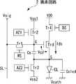
以下図面を参照して本発明の実施の形態を詳細に説明する。図1は本発明にかかる表示装置の全体構成を示すブロック図である。図示する様に、本表示装置は基本的に画素アレイ部1とスキャナ部と信号部とで構成されている。スキャナ部と信号部とで駆動部を構成する。画素アレイ部1は、行状に配された第1走査線WS、第2走査線DS、第3走査線AZ1及び第4走査線AZ2と、列状に配された信号線SLと、これらの走査線WS,DS,AZ1,AZ2及び信号線SLに接続した行列状の画素回路2と、各画素回路2の動作に必要な第1電位Vss1,第2電位Vss2及び第3電位VDDを供給する複数の電源線とからなる。信号部は水平セレクタ3からなり、信号線SLに映像信号を供給する。スキャナ部は、ライトスキャナ4、ドライブスキャナ5、第一補正用スキャナ71及び第二補正用スキャナ72からなり、それぞれ第1走査線WS、第2走査線DS、第3走査線AZ1及び第4走査線AZ2に制御信号を供給して順次行毎に画素回路2を走査する。 Hereinafter, embodiments of the present invention will be described in detail with reference to the drawings. FIG. 1 is a block diagram showing the overall configuration of a display device according to the present invention. As shown in the figure, this display device basically includes a
図2は、図1に示した画像表示装置に組み込まれる画素の構成を示す回路図である。図示する様に画素回路2は、サンプリングトランジスタTr1と、ドライブトランジスタTrdと、第1スイッチングトランジスタTr2と、第2スイッチングトランジスタTr3と、第3スイッチングトランジスタTr4と、保持容量Csと、発光素子ELとを含む。サンプリングトランジスタTr1は、所定のサンプリング期間に走査線WSから供給される制御信号に応じ導通して信号線SLから供給された映像信号の信号電位を保持容量Csにサンプリングする。保持容量Csは、サンプリングされた映像信号の信号電位に応じてドライブトランジスタTrdのゲートGに入力電圧Vgsを印加する。ドライブトランジスタTrdは、入力電圧Vgsに応じた出力電流Idsを発光素子ELに供給する。発光素子ELは、所定の発光期間中ドライブトランジスタTrdから供給される出力電流Idsにより映像信号の信号電位に応じた輝度で発光する。 FIG. 2 is a circuit diagram showing a configuration of a pixel incorporated in the image display apparatus shown in FIG. As illustrated, the
第1スイッチングトランジスタTr2は、サンプリング期間(映像信号書込期間)に先立ち走査線AZ1から供給される制御信号に応じ導通してドライブトランジスタTrdの制御端であるゲートGを第1電位Vss1に設定する。第2スイッチングトランジスタTr3は、サンプリング期間に先立ち走査線AZ2から供給される制御信号に応じ導通してドライブトランジスタTrdの一方の電流端であるソースSを第2電位Vss2に設定する。第3スイッチングトランジスタTr4は、サンプリング期間に先立ち走査線DSから供給される制御信号に応じ導通してドライブトランジスタTrdの他方の電流端であるドレインを第3電位VDDに接続し、以ってドライブトランジスタTrdの閾電圧Vthに相当する電圧を保持容量Csに保持させて閾電圧Vthの影響を補正する。さらにこの第3スイッチングトランジスタTr4は、発光期間に再び走査線DSから供給される制御信号に応じ導通してドライブトランジスタTrdを第3電位VDDに接続して出力電流Idsを発光素子ELに流す。 The first switching transistor Tr2 conducts in response to a control signal supplied from the scanning line AZ1 prior to the sampling period (video signal writing period), and sets the gate G, which is the control terminal of the drive transistor Trd, to the first potential Vss1. . The second switching transistor Tr3 conducts in response to a control signal supplied from the scanning line AZ2 prior to the sampling period, and sets the source S, which is one current end of the drive transistor Trd, to the second potential Vss2. The third switching transistor Tr4 is turned on in response to the control signal supplied from the scanning line DS prior to the sampling period, and connects the drain which is the other current end of the drive transistor Trd to the third potential VDD. A voltage corresponding to the threshold voltage Vth of Trd is held in the holding capacitor Cs to correct the influence of the threshold voltage Vth. Further, the third switching transistor Tr4 is turned on again in response to the control signal supplied from the scanning line DS during the light emission period, connects the drive transistor Trd to the third potential VDD, and flows the output current Ids to the light emitting element EL.
以上の説明から明らかな様に、本画素回路2は、5個のトランジスタTr1ないしTr4及びTrdと1個の保持容量Csと1個の発光素子ELとで構成されている。トランジスタTr1〜Tr3とTrdはNチャネル型のポリシリコンTFTである。トランジスタTr4のみPチャネル型のポリシリコンTFTである。但し本発明はこれに限られるものではなく、Nチャネル型とPチャネル型のTFTを適宜混在させることができる。発光素子ELは例えばアノード及びカソードを備えたダイオード型の有機ELデバイスである。但し本発明はこれに限られるものではなく、発光素子は一般的に電流駆動で発光する全てのデバイスを含む。 As is clear from the above description, the
図3は、図2に示した画像表示装置から画素回路2の部分のみを取り出した模式図である。理解を容易にするため、サンプリングトランジスタTr1によってサンプリングされる映像信号の信号電位Vsigや、ドライブトランジスタTrdの入力電圧Vgs及び出力電流Ids、さらには発光素子ELが有する容量成分Coledなどを書き加えてある。以下図3に基づいて、本発明にかかる画素回路2の動作を説明する。 FIG. 3 is a schematic diagram in which only the
図4は、図3に示した画素回路のタイミングチャートである。図4のタイミングチャートを参照しながら、図1及び図2に示した本発明にかかる表示装置の動作を具体的に説明する。図4は、時間軸Tに沿って各走査線WS,AZ1,AZ2及びDSに印加される制御信号の波形を表してある。表記を簡略化する為、制御信号も対応する走査線の符号と同じ符号で表してある。トランジスタTr1,Tr2,Tr3はNチャネル型なので、走査線WS,AZ1,AZ2がそれぞれハイレベルの時オンし、ローレベルの時オフする。一方トランジスタTr4はPチャネル型なので、走査線DSがハイレベルの時オフし、ローレベルの時オンする。なおこのタイミングチャートは、各制御信号WS,AZ1,AZ2,DSの波形と共に、ドライブトランジスタTrdのゲートGの電位変化及びソースSの電位変化も表してある。 FIG. 4 is a timing chart of the pixel circuit shown in FIG. The operation of the display device according to the present invention shown in FIGS. 1 and 2 will be specifically described with reference to the timing chart of FIG. FIG. 4 shows the waveforms of control signals applied to the scanning lines WS, AZ1, AZ2, and DS along the time axis T. In order to simplify the notation, the control signals are also represented by the same reference numerals as the corresponding scanning lines. Since the transistors Tr1, Tr2 and Tr3 are N-channel type, they are turned on when the scanning lines WS, AZ1 and AZ2 are at a high level and turned off when the scanning lines are at a low level. On the other hand, since the transistor Tr4 is a P-channel type, it is turned off when the scanning line DS is at a high level and turned on when it is at a low level. This timing chart also shows the change in the potential of the gate G and the change in the potential of the source S of the drive transistor Trd, along with the waveforms of the control signals WS, AZ1, AZ2, and DS.
図4のタイミングチャートではタイミングT1〜T8までを1フィールド(1f)としてある。1フィールドの間に画素アレイの各行が一回順次走査される。タイミングチャートは、1行分の画素に印加される各制御信号WS,AZ1,AZ2,DSの波形を表してある。 In the timing chart of FIG. 4, timings T1 to T8 are defined as one field (1f). Each row of the pixel array is sequentially scanned once during one field. The timing chart shows the waveforms of the control signals WS, AZ1, AZ2, DS applied to the pixels for one row.
当該フィールドが始まる前のタイミングT0で、全ての制御線号WS,AZ1,AZ2,DSがローレベルにある。したがってNチャネル型のトランジスタTr1,Tr2,Tr3はオフ状態にある一方、Pチャネル型のトランジスタTr4のみオン状態である。したがってドライブトランジスタTrdはオン状態のトランジスタTr4を介して電源VDDに接続しているので、所定の入力電圧Vgsに応じて出力電流Idsを発光素子ELに供給している。したがってタイミングT0で発光素子ELは発光している。この時ドライブトランジスタTrdに印加される入力電圧Vgsは、ゲート電位(G)とソース電位(S)の差で表される。 At timing T0 before the field starts, all control line numbers WS, AZ1, AZ2, DS are at a low level. Therefore, the N-channel transistors Tr1, Tr2, Tr3 are in the off state, while only the P-channel transistor Tr4 is in the on state. Therefore, since the drive transistor Trd is connected to the power supply VDD via the transistor Tr4 in the on state, the output current Ids is supplied to the light emitting element EL according to the predetermined input voltage Vgs. Therefore, the light emitting element EL emits light at the timing T0. At this time, the input voltage Vgs applied to the drive transistor Trd is expressed by the difference between the gate potential (G) and the source potential (S).
当該フィールドが始まるタイミングT1で、制御信号DSがローレベルからハイレベルに切り替わる。これによりスイッチングトランジスタTr4がオフし、ドライブトランジスタTrdは電源VDDから切り離されるので、発光が停止し非発光期間に入る。したがってタイミングT1に入ると、全てのトランジスタTr1〜Tr4がオフ状態になる。 At the timing T1 when the field starts, the control signal DS is switched from the low level to the high level. As a result, the switching transistor Tr4 is turned off and the drive transistor Trd is disconnected from the power supply VDD, so that the light emission stops and the non-light emission period starts. Therefore, at the timing T1, all the transistors Tr1 to Tr4 are turned off.
続いてタイミングT2に進むと、制御信号AZ1及びAZ2がハイレベルになるので、スイッチングトランジスタTr2及びTr3がオンする。この結果、ドライブトランジスタTrdのゲートGが基準電位Vss1に接続し、ソースSが基準電位Vss2に接続される。ここでVss1−Vss2>Vthを満たしており、Vss1−Vss2=Vgs>Vthとする事で、その後タイミングT3で行われるVth補正の準備を行う。換言すると期間T2‐T3は、ドライブトランジスタTrdのリセット期間に相当する。また、発光素子ELの閾電圧をVthELとすると、VthEL>Vss2に設定されている。これにより、発光素子ELにはマイナスバイアスが印加され、いわゆる逆バイアス状態となる。この逆バイアス状態は、後で行うVth補正動作及び移動度補正動作を正常に行うために必要である。 Subsequently, at timing T2, since the control signals AZ1 and AZ2 are at a high level, the switching transistors Tr2 and Tr3 are turned on. As a result, the gate G of the drive transistor Trd is connected to the reference potential Vss1, and the source S is connected to the reference potential Vss2. Here, Vss1−Vss2> Vth is satisfied, and by setting Vss1−Vss2 = Vgs> Vth, preparation for Vth correction performed at timing T3 is performed. In other words, the period T2-T3 corresponds to a reset period of the drive transistor Trd. Further, when the threshold voltage of the light emitting element EL is VthEL, VthEL> Vss2 is set. Thereby, a minus bias is applied to the light emitting element EL, and a so-called reverse bias state is obtained. This reverse bias state is necessary for normally performing the Vth correction operation and the mobility correction operation to be performed later.
タイミングT3では制御信号AZ2をローレベルにし且つ直後制御信号DSもローレベルにしている。これによりトランジスタTr3がオフする一方トランジスタTr4がオンする。この結果ドレイン電流Idsが保持容量Csに流れ込み、Vth補正動作を開始する。この時ドライブトランジスタTrdのゲートGはVss1に保持されており、ドライブトランジスタTrdがカットオフするまで電流Idsが流れる。カットオフするとドライブトランジスタTrdのソース電位(S)はVss1−Vthとなる。ドレイン電流がカットオフした後のタイミングT4で制御信号DSを再びハイレベルに戻し、スイッチングトランジスタTr4をオフする。さらに制御信号AZ1もローレベルに戻し、スイッチングトランジスタTr2もオフする。この結果、保持容量CsにVthが保持固定される。この様にタイミングT3‐T4はドライブトランジスタTrdの閾電圧Vthを検出する期間である。ここでは、この検出期間T3‐T4をVth補正期間と呼んでいる。 At timing T3, the control signal AZ2 is set to the low level, and the control signal DS is also set to the low level. As a result, the transistor Tr3 is turned off while the transistor Tr4 is turned on. As a result, the drain current Ids flows into the storage capacitor Cs, and the Vth correction operation is started. At this time, the gate G of the drive transistor Trd is held at Vss1, and the current Ids flows until the drive transistor Trd is cut off. When cut off, the source potential (S) of the drive transistor Trd becomes Vss1-Vth. At timing T4 after the drain current is cut off, the control signal DS is returned to the high level again, and the switching transistor Tr4 is turned off. Further, the control signal AZ1 is also returned to the low level, and the switching transistor Tr2 is also turned off. As a result, Vth is held and fixed in the holding capacitor Cs. Thus, the timing T3-T4 is a period for detecting the threshold voltage Vth of the drive transistor Trd. Here, this detection period T3-T4 is called a Vth correction period.
この様にVth補正を行った後タイミングT5で制御信号WSをハイレベルに切り替え、サンプリングトランジスタTr1をオンして映像信号Vsigを保持容量Csに書き込む。発光素子ELの等価容量Coledに比べて保持容量Csは充分に小さい。この結果、映像信号Vsigのほとんど大部分が保持容量Csに書き込まれる。正確には、Vss1に対するVsigの差分Vsig−Vss1が保持容量Csに書き込まれる。したがってドライブトランジスタTrdのゲートGとソースS間の電圧Vgsは、先に検出保持されたVthと今回サンプリングされたVsig−Vss1を加えたレベル(Vsig−Vss1+Vth)となる。以降説明簡易化の為Vss1=0Vとすると、ゲート/ソース間電圧Vgsは図4のタイミングチャートに示すようにVsig+Vthとなる。かかる映像信号Vsigのサンプリングは制御信号WSがローレベルに戻るタイミングT7まで行われる。すなわちタイミングT5‐T7がサンプリング期間(映像信号書込期間)に相当する。 After performing the Vth correction in this way, the control signal WS is switched to the high level at timing T5, the sampling transistor Tr1 is turned on, and the video signal Vsig is written in the storage capacitor Cs. The storage capacitor Cs is sufficiently smaller than the equivalent capacitor Coled of the light emitting element EL. As a result, most of the video signal Vsig is written in the storage capacitor Cs. Precisely, the difference Vsig−Vss1 of Vsig with respect to Vss1 is written in the storage capacitor Cs. Therefore, the voltage Vgs between the gate G and the source S of the drive transistor Trd becomes a level (Vsig−Vss1 + Vth) obtained by adding Vth previously detected and held and Vsig−Vss1 sampled this time. In the following description, assuming Vss1 = 0V for simplification of explanation, the gate / source voltage Vgs becomes Vsig + Vth as shown in the timing chart of FIG. The sampling of the video signal Vsig is performed until timing T7 when the control signal WS returns to the low level. That is, the timing T5-T7 corresponds to the sampling period (video signal writing period).
サンプリング期間の終了するタイミングT7より前のタイミングT6で制御信号DSがローレベルとなりスイッチングトランジスタTr4がオンする。これによりドライブトランジスタTrdが電源VDDに接続されるので、画素回路は非発光期間から発光期間に進む。この様にサンプリングトランジスタTr1がまだオン状態で且つスイッチングトランジスタTr4がオン状態に入った期間T6‐T7で、ドライブトランジスタTrdの移動度補正を行う。即ち本発明では、サンプリング期間の後部分と発光期間の先頭部分とが重なる期間T6‐T7で移動度補正を行っている。なお、この移動度補正を行う発光期間の先頭では、発光素子ELは実際には逆バイアス状態にあるので発光する事はない。この移動度補正期間T6‐T7では、ドライブトランジスタTrdのゲートGが映像信号Vsigのレベルに固定された状態で、ドライブトランジスタTrdにドレイン電流Idsが流れる。ここでVss1−Vth<VthELと設定しておく事で、発光素子ELは逆バイアス状態におかれる為、ダイオード特性ではなく単純な容量特性を示すようになる。よってドライブトランジスタTrdに流れる電流Idsは保持容量Csと発光素子ELの等価容量Coledの両者を結合した容量C=Cs+Coledに書き込まれていく。これによりドライブトランジスタTrdのソース電位(S)は上昇していく。図4のタイミングチャートではこの上昇分をΔVで表してある。この上昇分ΔVは結局保持容量Csに保持されたゲート/ソース間電圧Vgsから差し引かれる事になるので、負帰還をかけた事になる。この様にドライブトランジスタTrdの出力電流Idsを同じくドライブトランジスタTrdの入力電圧Vgsに負帰還する事で、移動度μを補正する事が可能である。なお負帰還量ΔVは移動度補正期間T6‐T7の時間幅tを調整する事で最適化可能である。 At timing T6 before the end of the sampling period T7, the control signal DS becomes low level and the switching transistor Tr4 is turned on. As a result, the drive transistor Trd is connected to the power supply VDD, so that the pixel circuit proceeds from the non-light emitting period to the light emitting period. In this manner, the mobility correction of the drive transistor Trd is performed in the period T6-T7 in which the sampling transistor Tr1 is still on and the switching transistor Tr4 is on. That is, in the present invention, the mobility correction is performed in the period T6-T7 in which the rear part of the sampling period and the head part of the light emission period overlap. Note that, at the beginning of the light emission period in which the mobility correction is performed, the light emitting element EL is actually in a reverse bias state, and thus does not emit light. In the mobility correction period T6-T7, the drain current Ids flows through the drive transistor Trd while the gate G of the drive transistor Trd is fixed at the level of the video signal Vsig. Here, by setting Vss1−Vth <VthEL, the light emitting element EL is placed in a reverse bias state, so that it exhibits simple capacitance characteristics instead of diode characteristics. Therefore, the current Ids flowing through the drive transistor Trd is written to the capacitor C = Cs + Coled obtained by combining both the storage capacitor Cs and the equivalent capacitor Coled of the light emitting element EL. As a result, the source potential (S) of the drive transistor Trd increases. In the timing chart of FIG. 4, this increase is represented by ΔV. Since this increase ΔV is eventually subtracted from the gate / source voltage Vgs held in the holding capacitor Cs, negative feedback is applied. In this way, the mobility μ can be corrected by negatively feeding back the output current Ids of the drive transistor Trd to the input voltage Vgs of the drive transistor Trd. The negative feedback amount ΔV can be optimized by adjusting the time width t of the mobility correction period T6-T7.
タイミングT7では制御信号WSがローレベルとなりサンプリングトランジスタTr1がオフする。この結果ドライブトランジスタTrdのゲートGは信号線SLから切り離される。映像信号Vsigの印加が解除されるので、ドライブトランジスタTrdのゲート電位(G)は上昇可能となり、ソース電位(S)と共に上昇していく。その間保持容量Csに保持されたゲート/ソース間電圧Vgsは(Vsig−ΔV+Vth)の値を維持する。ソース電位(S)の上昇に伴い、発光素子ELの逆バイアス状態は解消されるので、出力電流Idsの流入により発光素子ELは実際に発光を開始する。この時のドレイン電流Ids対ゲート電圧Vgsの関係は、先のトランジスタ特性式1のVgsにVsig−ΔV+Vthを代入する事で、以下の式2のように与えられる。
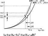
Ids=kμ(Vgs−Vth)2=kμ(Vsig−ΔV)2・・・式2
上記式2において、k=(1/2)(W/L)Coxである。この特性式2からVthの項がキャンセルされており、発光素子ELに供給される出力電流IdsはドライブトランジスタTrdの閾電圧Vthに依存しない事が分かる。基本的にドレイン電流Idsは映像信号の信号電圧Vsigによって決まる。換言すると、発光素子ELは映像信号Vsigに応じた輝度で発光する事になる。その際Vsigは負帰還量ΔVで補正されている。この補正量ΔVは丁度特性式2の係数部に位置する移動度μの効果を打ち消すように働く。したがって、ドレイン電流Idsは実質的に映像信号Vsigのみに依存する事になる。At timing T7, the control signal WS becomes low level and the sampling transistor Tr1 is turned off. As a result, the gate G of the drive transistor Trd is disconnected from the signal line SL. Since the application of the video signal Vsig is cancelled, the gate potential (G) of the drive transistor Trd can be increased and increases with the source potential (S). Meanwhile, the gate / source voltage Vgs held in the holding capacitor Cs maintains a value of (Vsig−ΔV + Vth). As the source potential (S) rises, the reverse bias state of the light emitting element EL is canceled, so that the light emitting element EL actually starts to emit light by the inflow of the output current Ids. The relationship between the drain current Ids and the gate voltage Vgs at this time is given by the
Ids = kμ (Vgs−Vth)2 = kμ (Vsig−ΔV)2
In the
最後にタイミングT8に至ると制御信号DSがハイレベルとなってスイッチングトランジスタTr4がオフし、発光が終了すると共に当該フィールドが終わる。この後次のフィールドに移って再びVth補正動作、移動度補正動作及び発光動作が繰り返される事になる。 Finally, when the timing T8 is reached, the control signal DS becomes high level, the switching transistor Tr4 is turned off, the light emission ends, and the field ends. Thereafter, the operation proceeds to the next field, and the Vth correction operation, the mobility correction operation, and the light emission operation are repeated again.
図5は、移動度補正期間T6‐T7における画素回路2の状態を示す回路図である。図示するように、移動度補正期間T6‐T7では、サンプリングトランジスタTr1及びスイッチングトランジスタTr4がオンしている一方、残りのスイッチングトランジスタTr2及びTr3がオフしている。この状態でドライブトランジスタTr4のソース電位(S)はVss1−Vthである。このソース電位(S)は発光素子ELのアノード電位でもある。前述したようにVss1−Vth<VthELと設定しておく事で、発光素子ELは逆バイアス状態におかれ、ダイオード特性ではなく単純な容量特性を示す事になる。よってドライブトランジスタTrdに流れる電流Idsは保持容量Csと発光素子ELの等価容量Coledとの合成容量C=Cs+Coledに流れ込む事になる。換言すると、ドレイン電流Idsの一部が保持容量Csに負帰還され、移動度の補正が行われる。 FIG. 5 is a circuit diagram showing a state of the
図6は上述したトランジスタ特性式2をグラフ化したものであり、縦軸にIdsを取り横軸にVsigを取ってある。このグラフの下方に特性式2も合わせて示してある。図6のグラフは、画素1と画素2を比較した状態で特性カーブを描いてある。画素1のドライブトランジスタの移動度μは相対的に大きい。逆に画素2に含まれるドライブトランジスタの移動度μは相対的に小さい。この様にドライブトランジスタをポリシリコン薄膜トランジスタなどで構成した場合、画素間で移動度μがばらつく事は避けられない。例えば両画素1,2に同レベルの映像信号の信号電位Vsigを書き込んだ場合、何ら移動度の補正を行わないと、移動度μの大きい画素1に流れる出力電流Ids1´は、移動度μの小さい画素2に流れる出力電流Ids2´に比べて大きな差が生じてしまう。この様に移動度μのばらつきに起因して出力電流Idsの間に大きな差が生じるので、スジムラが発生し画面のユニフォーミティを損なう事になる。 FIG. 6 is a graph of the above-described transistor
そこで本発明では出力電流を入力電圧側に負帰還させる事で移動度のばらつきをキャンセルしている。先のトランジスタ特性式1から明らかなように、移動度が大きいとドレイン電流Idsが大きくなる。したがって負帰還量ΔVは移動度が大きいほど大きくなる。図6のグラフに示すように、移動度μの大きな画素1の負帰還量ΔV1は移動度の小さな画素2の負帰還量ΔV2に比べて大きい。したがって、移動度μが大きいほど負帰還が大きくかかる事となって、ばらつきを抑制する事が可能である。図示するように、移動度μの大きな画素1でΔV1の補正をかけると、出力電流はIds1´からIds1まで大きく下降する。一方移動度μの小さな画素2の補正量ΔV2は小さいので、出力電流Ids2´はIds2までそれ程大きく下降しない。結果的に、Ids1とIds2は略等しくなり、移動度のばらつきがキャンセルされる。この移動度のばらつきのキャンセルは黒レベルから白レベルまでVsigの全範囲で行われるので、画面のユニフォーミティは極めて高くなる。以上をまとめると、移動度の異なる画素1と2があった場合、移動度の大きい画素1の補正量ΔV1は移動度の小さい画素2の補正量ΔV2に対して小さくなる。つまり移動度が大きいほどΔVが大きくIdsの減少値は大きくなる。これにより移動度の異なる画素電流値は均一化され、移動度のばらつきを補正する事ができる。 Therefore, in the present invention, the variation in mobility is canceled by negatively feeding back the output current to the input voltage side. As apparent from the previous transistor
以下参考の為、上述した移動度補正の数値解析を行う。図5に示したように、トランジスタTr1及びTr4がオンした状態で、ドライブトランジスタTrdのソース電位を変数Vに取って解析を行う。ドライブトランジスタTrdのソース電位(S)をVとすると、ドライブトランジスタTrdを流れるドレイン電流Idsは以下の式3に示す通りである。
またドレイン電流Idsと容量C(=Cs+Coled)の関係により、以下の式4に示す様にIds=dQ/dt=CdV/dtが成り立つ。
式4に式3を代入して両辺積分する。ここで、ソース電圧V初期状態は−Vthであり、移動度ばらつき補正時間(T6‐T7)をtとする。この微分方程式を解くと、移動度補正時間tに対する画素電流が以下の数式5のように与えられる。
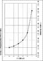
ところで最適な移動度補正時間は必ずしも一定ではなく、信号電圧に応じて最適移動度補正時間は変化する。図7は、この最適移動度補正時間と信号電圧との関係を示すグラフである。図から明らかなように、信号電圧が白レベルで高い時、最適移動度補正時間は比較的短い。信号電圧がグレーレベルでは最適移動度補正時間も長くなり、さらにブラックレベルでは最適移動度補正時間が一層延長する傾向にある。前述したように、移動度補正期間中、保持容量に負帰還する補正量ΔVは信号電圧Vsigに比例している。信号電圧が高いとその分負帰還量も大きくなるので、最適移動度補正時間は短くなる傾向にある。逆に信号電圧が下がるとドライブトランジスタの電流供給能力が下がるため、十分な補正に必要な最適移動度補正時間は延びる傾向にある。 By the way, the optimum mobility correction time is not necessarily constant, and the optimum mobility correction time changes according to the signal voltage. FIG. 7 is a graph showing the relationship between the optimum mobility correction time and the signal voltage. As is clear from the figure, the optimum mobility correction time is relatively short when the signal voltage is high at the white level. When the signal voltage is at the gray level, the optimum mobility correction time tends to be longer, and when the signal voltage is at the black level, the optimum mobility correction time tends to be further extended. As described above, the correction amount ΔV that is negatively fed back to the storage capacitor during the mobility correction period is proportional to the signal voltage Vsig. When the signal voltage is high, the negative feedback amount increases accordingly, so that the optimum mobility correction time tends to be short. On the contrary, when the signal voltage decreases, the current supply capability of the drive transistor decreases, so that the optimum mobility correction time necessary for sufficient correction tends to be extended.
そこで本発明は、信号線SLに供給される映像信号の信号電位Vsigが高い時補正期間tが短くなる一方、信号線SLに供給される映像信号の信号電位Vsigが低い時補正期間tが長くなるように、自動的にサンプリングトランジスタWSのオフタイミングを調整している。この原理を図8に示す。 Therefore, according to the present invention, the correction period t is shortened when the signal potential Vsig of the video signal supplied to the signal line SL is high, while the correction period t is lengthened when the signal potential Vsig of the video signal supplied to the signal line SL is low. Thus, the OFF timing of the sampling transistor WS is automatically adjusted. This principle is shown in FIG.
図8の波形図は、移動度補正期間tを規定するスイッチングトランジスタTr4のオンタイミング及びサンプリングトランジスタTr1のオフタイミングを律する、制御信号DSの立下がり波形及び制御信号WSの立下り波形を表している。前述したように、スイッチングトランジスタTr4のゲートに印加される制御信号DSがVDD−|Vtp|を下回った時点で、スイッチングトランジスタTr4はオンし、移動度補正時間が開始する。 The waveform diagram of FIG. 8 shows the falling waveform of the control signal DS and the falling waveform of the control signal WS that regulate the ON timing of the switching transistor Tr4 and the OFF timing of the sampling transistor Tr1 that define the mobility correction period t. . As described above, when the control signal DS applied to the gate of the switching transistor Tr4 falls below VDD− | Vtp |, the switching transistor Tr4 is turned on and the mobility correction time starts.
一方サンプリングトランジスタTr1のゲートには制御信号WSが印加されている。その立下り波形は図示する様に、始め電源電位Vccから急峻に下がり、その後接地電位Vssに向かって緩やかに低下していく。ここでサンプリングトランジスタTr1のソースに印加される信号電位Vsig1が白レベルで高い時サンプリングトランジスタTr1のゲート電位はVsig1+Vtnまで速やかに降下するので、最適移動度補正時間t1は短くなる。信号電位がグレーレベルのVsig2になると、ゲート電位がVsig2+VtnまでVccから下がった時点でサンプリングトランジスタTr1がオフする。その結果グレーレベルのVsig2に対応した最適補正時間t2は、t1に比べて長くなる。さらに信号電位がブラックレベルに近いVsig3になると、最適移動度補正時間t3は、グレーレベルの時の最適移動度補正時間t2に比べ一層長くなる。 On the other hand, the control signal WS is applied to the gate of the sampling transistor Tr1. As shown in the figure, the falling waveform suddenly drops from the power supply potential Vcc and then gradually decreases toward the ground potential Vss. Here, when the signal potential Vsig1 applied to the source of the sampling transistor Tr1 is high at the white level, the gate potential of the sampling transistor Tr1 quickly drops to Vsig1 + Vtn, so that the optimum mobility correction time t1 is shortened. When the signal potential becomes the gray level Vsig2, the sampling transistor Tr1 is turned off when the gate potential drops from Vcc to Vsig2 + Vtn. As a result, the optimum correction time t2 corresponding to the gray level Vsig2 becomes longer than t1. Further, when the signal potential becomes Vsig3 close to the black level, the optimum mobility correction time t3 becomes longer than the optimum mobility correction time t2 at the gray level.
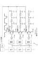
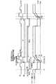
各階調毎に最適な移動度補正時間を自動的に設定するためには、走査線WSに印加される制御信号パルスの立下りを最適な形状に波形整形する必要がある。このために本発明は電源パルスを抜き取る方式のライトスキャナを採用しており、図9を参照してこれを説明する。図9は、ライトスキャナ4の出力部三段分と、これに接続される画素アレイ部1の三行分(3ライン分)を模式的に表している。 In order to automatically set the optimum mobility correction time for each gradation, it is necessary to shape the waveform of the falling edge of the control signal pulse applied to the scanning line WS into an optimum shape. For this purpose, the present invention employs a write scanner that extracts power pulses, which will be described with reference to FIG. FIG. 9 schematically shows three stages of the output section of the
ライトスキャナ4はシフトレジスタS/Rで構成されており、外部から入力されるクロック信号に応じて動作し、同じく外部から入力されるスタート信号を順次転走することで、各段毎に順次信号を出力している。シフトレジスタS/Rの各段にはNAND素子が接続されており、隣り合う段のS/Rから出力された順次信号をNAND処理して、制御信号WSの元になる矩形波形を生成している。この矩形波形はインバータを介して出力バッファに入力される。この出力バッファはシフトレジスタ側から供給される入力信号に応じて動作し、最終的な制御信号WSを対応する画素アレイ部1の走査線WSに供給している。なお本明細書では、NAND素子とインバータもシフトレジスタの一部を構成する要素として記述している。 The
出力バッファは電源電位Vccと接地電位Vssとの間に直列接続された一対のスイッチング素子からなる。本発明はこの出力バッファがインバータ構成となっており、一方のスイッチング素子がPチャネル型トランジスタPch(典型的にはPMOSトランジスタ)で、他方がNチャネル型トランジスタNch(典型的にはNMOSトランジスタ)からなる。なお各出力バッファに接続される画素アレイ部1側の各ラインは、等価回路的に抵抗成分Rと容量成分Cで表してある。 The output buffer includes a pair of switching elements connected in series between the power supply potential Vcc and the ground potential Vss. In the present invention, the output buffer has an inverter configuration, one switching element is a P-channel transistor Pch (typically a PMOS transistor) and the other is an N-channel transistor Nch (typically an NMOS transistor). Become. Each line on the
本発明は、出力バッファが外部のパルス電源から電源ラインに供給される電源パルスを抜き取って制御信号の決定波形を作る構成となっている。前述した様にこの出力バッファはインバータ構成で、電源ラインと接地電位Vssとの間にPチャネルトランジスタPchとNチャネルトランジスタNchが直列に接続されている。シフトレジスタS/R側からの入力信号に応じて出力バッファのPチャネルトランジスタPchがオンしたとき、電源ラインに供給されていた電源パルスの立下り波形を取り出し、これを制御信号WSの決定波形として、画素アレイ部1側に供給している。この様に出力バッファとは別に決定波形を含むパルスを作り、これを出力バッファの電源ラインに供給することで、所望の決定波形の制御信号WSを作り出すことが可能である。この場合出力バッファは、優勢スイッチング素子側となるPチャネルトランジスタPchがオンして劣勢スイッチング素子側となるNチャネルトランジスタNchがオフした時、外部から供給された電源パルスの立下り波形を取り出し、制御信号WSの決定波形として出力している。 In the present invention, the output buffer extracts the power supply pulse supplied from the external pulse power supply to the power supply line and creates a control signal decision waveform. As described above, this output buffer has an inverter configuration, and a P-channel transistor Pch and an N-channel transistor Nch are connected in series between the power supply line and the ground potential Vss. When the P-channel transistor Pch of the output buffer is turned on according to the input signal from the shift register S / R side, the falling waveform of the power supply pulse supplied to the power supply line is extracted and this is used as the determination waveform of the control signal WS. , And supplied to the
ここで抜き取られる電源パルスのレベルが立下りに沿って小さくなるに従い、出力バッファのPチャネルトランジスタPchの動作Vgsが小さくなっていく。動作Vgsが小さくなるにつれ抜き取られた電源パルスの立下り波形(パルストランジェント)はPチャネルトランジスタPchの特性ばらつきの影響を受けやすくなる。特にPチャネルトランジスタPchの閾電圧Vtpのばらつきの影響を受け、この結果移動度補正時間にばらつきが生じてしまう。特に映像信号のレベルが高い白階調では補正時間tが短いため、このばらつきが顕著に現れて筋が発生してしまう。 As the level of the power supply pulse extracted here becomes smaller along the falling edge, the operation Vgs of the P-channel transistor Pch of the output buffer becomes smaller. The falling waveform (pulse transient) of the power supply pulse extracted as the operation Vgs becomes small is easily affected by the characteristic variation of the P-channel transistor Pch. In particular, the mobility correction time varies due to the influence of variations in the threshold voltage Vtp of the P-channel transistor Pch. In particular, since the correction time t is short in a white gradation with a high level of the video signal, this variation appears remarkably and streaks occur.
そこで本発明は、ライトスキャナの出力バッファのトランジェントばらつきを抑制するため、出力バッファのPチャネルトランジスタPchに印加する入力信号のローレベルVssを電源パルスのローレベルVsspよりも低い値に設定している。 Therefore, the present invention sets the low level Vss of the input signal applied to the P-channel transistor Pch of the output buffer to a value lower than the low level Vssp of the power supply pulse in order to suppress the transient variation of the output buffer of the write scanner. .
図10は、図9に示したライトスキャナの動作説明に供するタイミングチャートである。図示するように1H周期で変動する電源パルスの列が外部のパルス電源からライトスキャナの出力バッファの電源ラインに入力されてくる。この電源パルスは高電位Vccと低電位Vsspとの間で電位が変化している。これに合わせて出力バッファを構成するインバータにシフトレジスタの出力部を構成するNAND素子及びインバータから入力パルスが印加される。タイミングチャートは、N−1段目及びN段目のインバータに供給される入力パルスを表している。図示するようにこの入力パルスは高電位Vccと低電位Vssとの間でレベルが切換っている。これと時系列を合わせて、N−1段目及びN段目から供給される出力パルスを表してある。この出力パルスは対応するラインの走査線WSに印加される制御信号である。 FIG. 10 is a timing chart for explaining the operation of the write scanner shown in FIG. As shown in the figure, a power pulse train that fluctuates in a 1H cycle is input from an external pulse power supply to the power supply line of the output buffer of the write scanner. The power supply pulse changes in potential between the high potential Vcc and the low potential Vssp. In accordance with this, an input pulse is applied from the NAND element and the inverter constituting the output part of the shift register to the inverter constituting the output buffer. The timing chart represents input pulses supplied to the (N-1) th stage and Nth stage inverters. As shown in the figure, the level of this input pulse is switched between the high potential Vcc and the low potential Vss. The output pulses supplied from the (N−1) th stage and the Nth stage are shown together with this and the time series. This output pulse is a control signal applied to the scanning line WS of the corresponding line.
タイミングチャートから明らかなように、シフトレジスタの各段に対応した出力バッファは、入力パルスに応じて電源パルスを抜き取り、そのまま出力パルスとして対応する走査線WSに供給している。電源パルスは外部のパルス電源から供給されており、その立下り波形は予め最適に設定可能である。ライトスキャナはこの立下り波形をそのまま抜き取って制御信号パルスとしている。 As is apparent from the timing chart, the output buffer corresponding to each stage of the shift register extracts the power supply pulse in accordance with the input pulse and supplies it directly to the corresponding scanning line WS as the output pulse. The power supply pulse is supplied from an external pulse power supply, and its falling waveform can be optimally set in advance. The write scanner extracts this falling waveform as it is and uses it as a control signal pulse.
本発明の特徴として、ライトスキャナは、電源パルスの低電位Vsspよりも入力信号の低電位Vssが低くなるように電位設定している。より好ましくは、電源パルスの低電位Vsspと入力信号の低電位Vssとの差がPチャネルトランジスタPchの閾電圧Vtpの絶対値を超えるように電位設定する。即ちVss<Vssp−|Vtp|の条件を満たす。ここで、VssはPチャネルトランジスタPchのゲート側に印加され、VsspはPチャネルトランジスタPchのソース側に印加されている。さらに好ましくは可能な限りVssの値を低く設定することが良い。かかる電位設定により、出力バッファのPチャネルトランジスタPchで電源パルスを抜き取ったとき、PチャネルトランジスタPchのゲート/ソース間電圧Vgsは大きくなり、抜き取るべき電源パルスのローレベルがVsspであってもPチャネルトランジスタPchのVgsを大きく維持することができ、その分Vtpばらつきを抑制することが可能である。以上により電源パルス抜き取り方式のライトスキャナにおいて、移動度補正時間のばらつきを抑制することが可能となり、全階調でユニフォーミティの高い画面を得ることができる。 As a feature of the present invention, the write scanner sets the potential so that the low potential Vss of the input signal is lower than the low potential Vssp of the power supply pulse. More preferably, the potential is set such that the difference between the low potential Vssp of the power supply pulse and the low potential Vss of the input signal exceeds the absolute value of the threshold voltage Vtp of the P-channel transistor Pch. That is, the condition Vss <Vssp− | Vtp | is satisfied. Here, Vss is applied to the gate side of the P-channel transistor Pch, and Vssp is applied to the source side of the P-channel transistor Pch. More preferably, the Vss value is set as low as possible. With this potential setting, when the power supply pulse is extracted by the P-channel transistor Pch of the output buffer, the gate-source voltage Vgs of the P-channel transistor Pch becomes large, and even if the power pulse to be extracted is at the low level Vssp, the P-channel Vgs of the transistor Pch can be kept large, and Vtp variation can be suppressed accordingly. As described above, in the power pulse extraction type light scanner, it is possible to suppress variation in mobility correction time, and a screen with high uniformity can be obtained in all gradations.
図11は、図9に示したライトスキャナから出力される制御信号WSの立下り波形を示した波形図である。但し電源パルスのローレベル(低電位)と出力バッファに供給する入力信号のローレベル(低電位)が等しい場合(Vss=Vssp)を示す参考図である。この参考図は時間軸を合わせてドライブスキャナ5から出力される制御信号DSの立下り波形も表してある。 FIG. 11 is a waveform diagram showing a falling waveform of the control signal WS output from the write scanner shown in FIG. However, it is a reference diagram showing a case where the low level (low potential) of the power supply pulse is equal to the low level (low potential) of the input signal supplied to the output buffer (Vss = Vssp). This reference diagram also shows the falling waveform of the control signal DS output from the
図9に示したライトスキャナは電源パルス抜き取り方式を採用しており、基本的には電源パルスの立下り波形をそのまま抜き取って制御信号WSの立下り波形にすることができる。しかしながら電位設定をVss=Vsspとしてしまうと、出力バッファを構成するインバータのトランジスタの動作特性の影響を受けて歪が生じてしまう。図11の制御信号WSの波形図は、標準位相を(1)で表し、特に歪が大きい場合の波形をばらつきワースト位相(2)で表してある。 The light scanner shown in FIG. 9 employs a power supply pulse extraction method. Basically, the falling waveform of the power supply pulse can be extracted as it is to obtain the falling waveform of the control signal WS. However, if the potential is set to Vss = Vssp, distortion occurs due to the influence of the operation characteristics of the transistors of the inverter constituting the output buffer. In the waveform diagram of the control signal WS in FIG. 11, the standard phase is represented by (1), and the waveform particularly when the distortion is large is represented by the variation worst phase (2).
図9に示したように出力バッファに対する入力がローレベルになったとき、出力バッファを構成するインバータのPチャネルトランジスタが導通して、電源パルスを抜き取っている。ここで抜き取られた電源パルスのレベルが小さくなるにつれ、Pチャネルトランジスタの動作中にゲート/ソース間に加わる電圧Vgsが小さくなってしまう。この動作Vgsが小さくなるにつれ抜き取られた電源パルスのトランジェントは、Pチャネルトランジスタの特性ばらつきの影響を受けやすくなり、補正時間にばらつきが生じてしまう。図示の例では、標準位相(1)の場合に比べ、バラツキワースト位相(2)のとき制御信号WSの立下りに応じてサンプリングトランジスタTr1がオフするタイミングが後方にシフトするため、移動度補正時間はその分長くなってしまう。特に白階調では最適な補正時間が短いため、このばらつきが顕著に現れこのままでは筋ムラが発生してしまう。 As shown in FIG. 9, when the input to the output buffer becomes low level, the P-channel transistor of the inverter constituting the output buffer becomes conductive, and the power supply pulse is extracted. As the level of the power supply pulse extracted here decreases, the voltage Vgs applied between the gate and source during the operation of the P-channel transistor decreases. The transient of the power supply pulse extracted as the operation Vgs becomes small is easily influenced by the characteristic variation of the P-channel transistor, and the correction time varies. In the example shown in the figure, the timing for turning off the sampling transistor Tr1 is shifted backward in accordance with the fall of the control signal WS in the case of the dispersion worst phase (2) as compared with the case of the standard phase (1). Will be longer. In particular, since the optimum correction time is short for white gradations, this variation appears remarkably and streak unevenness occurs.
図12は、本発明にかかる表示装置の第2実施形態の全体構成を示すブロック図である。図示するように、本表示装置は、画素アレイ部1とこれを駆動する駆動部とからなる。画素アレイ部1は、行状の走査線WSと、列状の信号線(信号ライン)SLと、両者が交差する部分に配された行列状の画素2と、各画素2の各行に対応して配された給電線(電源ライン)VLとを備えている。なお本例は、各画素2にRGB三原色のいずれかが割り当てられており、カラー表示が可能である。但しこれに限られるものではなく、単色表示のデバイスも含む。駆動部は、各走査線WSに順次制御信号を供給して画素2を行単位で線順次走査するライトスキャナ4と、この線順次走査に合わせて各給電線VLに第1電位と第2電位で切換る電源電圧を供給する電源スキャナ6と、この線順次走査に合わせて列状の信号線SLに映像信号となる信号電位と基準電位を供給する信号セレクタ(水平セレクタ)3とを備えている。 FIG. 12 is a block diagram showing the overall configuration of the second embodiment of the display device according to the present invention. As shown in the figure, the display device includes a
図13は、図12に示した表示装置に含まれる画素2の具体的な構成及び結線関係を示す回路図である。図示するように、この画素2は有機ELデバイスなどで代表される発光素子ELと、サンプリングトランジスタTr1と、ドライブトランジスタTrdと、保持容量Csとを含む。サンプリングトランジスタTr1は、その制御端(ゲート)が対応する走査線WSに接続し、一対の電流端(ソース及びドレイン)の一方が対応する信号線SLに接続し、他方がドライブトランジスタTrdの制御端(ゲートG)に接続する。ドライブトランジスタTrdは、一対の電流端(ソースS及びドレイン)の一方が発光素子ELに接続し、他方が対応する給電線VLに接続している。本例では、ドライブトランジスタTrdがNチャネル型であり、そのドレインが給電線VLに接続する一方、ソースSが出力ノードとして発光素子ELのアノードに接続している。発光素子ELのカソードは所定のカソード電位Vcathに接続している。保持容量CsはドライブトランジスタTrdのソースSとゲートGの間に接続している。 FIG. 13 is a circuit diagram showing a specific configuration and connection relationship of the
かかる構成において、サンプリングトランジスタTr1は走査線WSから供給された制御信号に応じて導通し、信号線SLから供給された信号電位をサンプリングして保持容量Csに保持する。ドライブトランジスタTrdは、第1電位(高電位Vdd)にある給電線VLから電流の供給を受け保持容量Csに保持された信号電位に応じて駆動電流を発光素子ELに流す。ライトスキャナ4は、信号線SLが信号電位にある時間帯にサンプリングトランジスタTr1を導通状態にするため、所定のパルス幅の制御信号を制御線WSに出力し、以って保持容量Csに信号電位を保持すると同時にドライブトランジスタTrdの移動度μに対する補正を信号電位に加える。この後ドライブトランジスタTrdは保持容量Csに書き込まれた信号電位Vsigに応じた駆動電流を発光素子ELに供給し、発光動作に入る。 In such a configuration, the sampling transistor Tr1 is turned on in response to a control signal supplied from the scanning line WS, samples the signal potential supplied from the signal line SL, and holds it in the holding capacitor Cs. The drive transistor Trd is supplied with current from the power supply line VL that is at the first potential (high potential Vdd), and flows drive current to the light emitting element EL in accordance with the signal potential held in the holding capacitor Cs. The
本画素回路2は、上述した移動度補正機能に加え閾電圧補正機能も備えている。即ち電源スキャナ6は、サンプリングトランジスタTr1が信号電位Vsigをサンプリングする前に、第1タイミングで給電線VLを第1電位(高電位Vdd)から第2電位(低電位Vss)に切換える。またライトスキャナ4は同じくサンプリングトランジスタTr1が信号電位Vsigをサンプリングする前に、第2タイミングでサンプリングトランジスタTr1を導通させて信号線SLから基準電位VrefをドライブトランジスタTrdのゲートGに印加すると共にドライブトランジスタTrdのソースSを第2電位(Vss)にセットする。電源スキャナ6は第2タイミングの後の第3タイミングで給電線VLを第2電位Vssから第1電位Vddに切換えて、ドライブトランジスタTrdの閾電圧Vthに相当する電圧を保持容量Csに保持する。かかる閾電圧補正機能により、本表示装置は画素毎にばらつくドライブトランジスタTrdの閾電圧Vthの影響をキャンセルすることができる。 The
本画素回路2は、さらにブートストラップ機能も備えている。即ちライトスキャナ4は保持容量Csに信号電位Vsigが保持された段階で走査線WSに対する制御信号の印加を解除し、サンプリングトランジスタTr1を非道通状態にしてドライブトランジスタTrdのゲートGを信号線SLから電気的に切り離し、以ってドライブトランジスタTrdのソースSの電位変動にゲートGの電位が連動し、ゲートGとソースS間の電圧Vgsを一定に維持することができる。 The
図14は、図13に示した画素回路2の動作説明に供するタイミングチャートである。時間軸を共通にして、走査線WSの電位変化、給電線VLの電位変化及び信号線SLの電位変化を表している。またこれらの電位変化と並行に、ドライブトランジスタのゲートG及びソースSの電位変化も表してある。 FIG. 14 is a timing chart for explaining the operation of the
前述したように走査線WSには、サンプリングトランジスタTr1をオンするための制御信号パルスが印加される。この制御信号パルスは画素アレイ部の線順次走査に合わせて1フィールド(1f)周期で走査線WSに印加される。電源線VLは同じように1フィールド周期で高電位Vddと低電位Vssとの間で切換る。信号線SLには1水平周期(1H)内で信号電位Vsigと基準電位Vrefが切換る映像信号を供給している。 As described above, the control signal pulse for turning on the sampling transistor Tr1 is applied to the scanning line WS. This control signal pulse is applied to the scanning line WS in one field (1f) cycle in accordance with the line sequential scanning of the pixel array section. Similarly, the power supply line VL is switched between the high potential Vdd and the low potential Vss in one field cycle. A video signal for switching the signal potential Vsig and the reference potential Vref within one horizontal period (1H) is supplied to the signal line SL.
図14のタイミングチャートに示すように、画素は前のフィールドの発光期間から当該フィールドの非発光期間に入り、そのあと当該フィールドの発光期間となる。この非発光期間で準備動作、閾電圧補正動作、信号書き込み動作、移動度補正動作などを行う。 As shown in the timing chart of FIG. 14, the pixel enters the non-light emission period of the field from the light emission period of the previous field, and then becomes the light emission period of the field. During this non-emission period, a preparation operation, a threshold voltage correction operation, a signal writing operation, a mobility correction operation, and the like are performed.
前フィールドの発光期間では、給電線VLが高電位Vddにあり、ドライブトランジスタTrdが駆動電流Idsを発光素子ELに供給している。駆動電流Idsは高電位Vddにある給電線VLからドライブトランジスタTrdを介して発光素子ELを通り、カソードラインに流れ込んでいる。 In the light emission period of the previous field, the power supply line VL is at the high potential Vdd, and the drive transistor Trd supplies the drive current Ids to the light emitting element EL. The drive current Ids flows from the power supply line VL at the high potential Vdd through the light emitting element EL through the drive transistor Trd to the cathode line.
続いて当該フィールドの非発光期間に入るとまずタイミングT1で給電線VLを高電位Vddから低電位Vssに切換える。これにより給電線VLはVssまで放電され、さらにドライブトランジスタTrdのソースSの電位はVssまで下降する。これにより発光素子ELのアノード電位(即ちドライブトランジスタTrdのソース電位)は逆バイアス状態となるため、駆動電流が流れなくなり消灯する。またドライブトランジスタのソースSの電位降下に連動してゲートGの電位も降下する。 Subsequently, when the non-light emission period of the field starts, first, at timing T1, the power supply line VL is switched from the high potential Vdd to the low potential Vss. As a result, the power supply line VL is discharged to Vss, and the potential of the source S of the drive transistor Trd drops to Vss. As a result, the anode potential of the light emitting element EL (that is, the source potential of the drive transistor Trd) is in a reverse bias state, so that the drive current does not flow and the light is turned off. Further, the potential of the gate G also drops in conjunction with the potential drop of the source S of the drive transistor.
続いてタイミングT2になると、走査線WSを低レベルから高レベルに切換えることで、サンプリングトランジスタTr1が導通状態になる。この時信号線SLは基準電位Vrefにある。よってドライブトランジスタTrdのゲートGの電位は導通したサンプリングトランジスタTr1を通じて信号線SLの基準電位Vrefとなる。この時ドライブトランジスタTrdのソースSの電位はVrefよりも十分低い電位Vssにある。この様にしてドライブトランジスタTrdのゲートGとソースSとの間の電圧VgsがドライブトランジスタTrdの閾電圧Vthより大きくなるように、初期化される。タイミングT1からタイミングT3までの期間T1‐T3はドライブトランジスタTrdのゲートG/ソースS間電圧Vgsを予めVth以上に設定する準備期間である。 Subsequently, at timing T2, the sampling transistor Tr1 becomes conductive by switching the scanning line WS from the low level to the high level. At this time, the signal line SL is at the reference potential Vref. Therefore, the potential of the gate G of the drive transistor Trd becomes the reference potential Vref of the signal line SL through the conducting sampling transistor Tr1. At this time, the potential of the source S of the drive transistor Trd is at a potential Vss sufficiently lower than Vref. In this way, the voltage Vgs between the gate G and the source S of the drive transistor Trd is initialized so as to be larger than the threshold voltage Vth of the drive transistor Trd. A period T1-T3 from the timing T1 to the timing T3 is a preparation period in which the gate G / source S voltage Vgs of the drive transistor Trd is set to Vth or higher in advance.
この後タイミングT3になると、給電線VLが低電位Vssから高電位Vddに遷移し、ドライブトランジスタTrdのソースSの電位が上昇を開始する。やがてドリライブトランジスタTrdのゲートG/ソースS間電圧Vgsが閾電圧Vthとなった所で電流がカットオフする。この様にしてドライブトランジスタTrdの閾電圧Vthに相当する電圧が保持容量Csに書き込まれる。これが閾電圧補正動作である。この時電流がもっぱら保持容量Cs側に流れ、発光素子ELには流れないようにするため、発光素子ELがカットオフとなるようにカソード電位Vcathを設定しておく。この閾電圧補正動作はタイミングT4で信号線SLの電位がVrefからVsigに切換るまでの間に完了する。タイミングT3からタイミングT4までの期間T3‐T4が移動度補正期間となる。 Thereafter, at timing T3, the power supply line VL changes from the low potential Vss to the high potential Vdd, and the potential of the source S of the drive transistor Trd starts to rise. Eventually, the current is cut off when the voltage Vgs between the gate G and the source S of the drive transistor Trd becomes the threshold voltage Vth. In this way, a voltage corresponding to the threshold voltage Vth of the drive transistor Trd is written into the storage capacitor Cs. This is the threshold voltage correction operation. At this time, the cathode potential Vcath is set so that the light emitting element EL is cut off in order to prevent the current from flowing to the storage capacitor Cs and not to the light emitting element EL. This threshold voltage correction operation is completed until the potential of the signal line SL is switched from Vref to Vsig at timing T4. A period T3-T4 from timing T3 to timing T4 is a mobility correction period.
タイミングT4では信号線SLが基準電位Vrefから信号電位Vsigに切換る。この時サンプリングトランジスタTr1は引き続き導通状態にある。よってドライブトランジスタTrdのゲートGの電位は信号電位Vsigになる。ここで発光素子ELは始めカットオフ状態(ハイインピーダンス状態)にあるためドライブトランジスタTrdのドレインとソースの間に流れる電流はもっぱら保持容量Csと発光素子ELの等価容量に流れ込み、充電を開始する。この後サンプリングトランジスタTr1がオフするタイミングT5までに、ドライブトランジスタTrdのソースSの電位はΔVだけ上昇する。この様にして映像信号の信号電位VsigがVthに足し込まれる形で保持容量Csに書き込まれると共に移動度補正用の電圧ΔVが保持容量Csに保持された電圧から差し引かれる。よってタイミングT4からタイミングT5までの期間T4‐T5が信号書き込み期間/移動度補正期間となる。この様に信号書き込み期間T4‐T5では信号電位Vsigの書き込みと補正量ΔVの調整が同時に行われる。Vsigが高いほどドライブトランジスタTrdが供給する電流Idsは大きくなり、ΔVの絶対値も大きくなる。したがって発光輝度レベルに応じた移動度補正が行われる。Vsigを一定とした場合、ドライブトランジスタTrdの移動度μが大きいほどΔVの絶対値が大きくなる。換言すると移動度μが大きいほど保持容量Csに対する負帰還量ΔVが大きくなるので、画素毎の移動度μのばらつきを取り除くことができる。 At timing T4, the signal line SL is switched from the reference potential Vref to the signal potential Vsig. At this time, the sampling transistor Tr1 is still in a conductive state. Therefore, the potential of the gate G of the drive transistor Trd becomes the signal potential Vsig. Here, since the light emitting element EL is initially in a cut-off state (high impedance state), the current flowing between the drain and source of the drive transistor Trd flows exclusively into the holding capacitor Cs and the equivalent capacity of the light emitting element EL, and charging is started. Thereafter, by the timing T5 when the sampling transistor Tr1 is turned off, the potential of the source S of the drive transistor Trd rises by ΔV. In this way, the signal potential Vsig of the video signal is written to the storage capacitor Cs in a form added to Vth, and the mobility correction voltage ΔV is subtracted from the voltage stored in the storage capacitor Cs. Therefore, a period T4-T5 from timing T4 to timing T5 is a signal writing period / mobility correction period. Thus, in the signal writing period T4-T5, the writing of the signal potential Vsig and the adjustment of the correction amount ΔV are performed simultaneously. As Vsig increases, the current Ids supplied from the drive transistor Trd increases and the absolute value of ΔV also increases. Therefore, the mobility correction according to the light emission luminance level is performed. When Vsig is constant, the absolute value of ΔV increases as the mobility μ of the drive transistor Trd increases. In other words, the larger the mobility μ is, the larger the negative feedback amount ΔV with respect to the storage capacitor Cs is, so that variation in the mobility μ for each pixel can be removed.
最後にタイミングT5になると、前述したように走査線WSが低レベル側に遷移し、サンプリングトランジスタTr1はオフ状態となる。これによりドライブトランジスタTrdのゲートGは信号線SLから切り離される。同時にドレイン電流Idsが発光素子ELを流れ始める。これにより発光素子ELのアノード電位は駆動電流Idsに応じて上昇する。発光素子ELのアノード電位の上昇は、即ちドライブトランジスタTrdのソースSの電位上昇に他ならない。ドライブトランジスタTrdのソースSの電位が上昇すると、保持容量Csのブートストラップ動作によりドライブトランジスタTrdのゲートGの電位も連動して上昇する。ゲート電位の上昇量はソース電位の上昇量に等しくなる。ゆえに発光期間中ドライブトランジスタTrdのゲートG/ソースS間電圧Vgsは一定に保持される。このVgsの値は信号電位Vsigに閾電圧Vth及び移動量μの補正をかけたものとなっている。 Finally, at timing T5, as described above, the scanning line WS shifts to the low level side, and the sampling transistor Tr1 is turned off. As a result, the gate G of the drive transistor Trd is disconnected from the signal line SL. At the same time, the drain current Ids starts to flow through the light emitting element EL. As a result, the anode potential of the light emitting element EL rises according to the drive current Ids. The increase in the anode potential of the light emitting element EL is none other than the increase in the potential of the source S of the drive transistor Trd. When the potential of the source S of the drive transistor Trd rises, the potential of the gate G of the drive transistor Trd also rises in conjunction with the bootstrap operation of the storage capacitor Cs. The amount of increase in gate potential is equal to the amount of increase in source potential. Therefore, the voltage Vgs between the gate G and the source S of the drive transistor Trd is kept constant during the light emission period. The value of Vgs is obtained by correcting the signal potential Vsig with the threshold voltage Vth and the movement amount μ.
この第2実施形態においても、移動度補正時間は信号線SLの電位がVrefからVsigに切換る第1タイミングから、制御信号WSが立下がってサンプリングトランジスタTr1がオフする第2タイミングまでの期間となっている。信号電位Vsigのレベルに応じて移動度補正時間を適応制御するため、本実施形態においても制御信号WSの立下り波形を適切に整形することが好ましく、図9に示したライトスキャナを採用している。ここでも電源パルスの低電位Vsspよりも出力バッファに印加する入力信号の低電位Vssが低くなるように電位設定することで、制御信号WSの立下り波形の歪を抑制している。 Also in the second embodiment, the mobility correction time is the period from the first timing when the potential of the signal line SL is switched from Vref to Vsig to the second timing when the control signal WS falls and the sampling transistor Tr1 is turned off. It has become. In order to adaptively control the mobility correction time according to the level of the signal potential Vsig, it is preferable to appropriately shape the falling waveform of the control signal WS in this embodiment as well, and the light scanner shown in FIG. 9 is adopted. Yes. Also here, the potential of the input signal applied to the output buffer is set to be lower than the low potential Vssp of the power supply pulse, thereby suppressing the distortion of the falling waveform of the control signal WS.
本発明にかかる表示装置は、図15に示すような薄膜デバイス構成を有する。本図は、絶縁性の基板に形成された画素の模式的な断面構造を表している。図示するように、画素は、複数の薄膜トランジタを含むトランジスター部(図では1個のTFTを例示)、保持容量などの容量部及び有機EL素子などの発光部とを含む。基板の上にTFTプロセスでトランジスター部や容量部が形成され、その上に有機EL素子などの発光部が積層されている。その上に接着剤を介して透明な対向基板を貼り付けてフラットパネルとしている。 The display device according to the present invention has a thin film device configuration as shown in FIG. This figure shows a schematic cross-sectional structure of a pixel formed on an insulating substrate. As shown in the figure, the pixel includes a transistor part (a single TFT is illustrated in the figure) including a plurality of thin film transistors, a capacitor part such as a storage capacitor, and a light emitting part such as an organic EL element. A transistor portion and a capacitor portion are formed on a substrate by a TFT process, and a light emitting portion such as an organic EL element is laminated thereon. A transparent counter substrate is pasted thereon via an adhesive to form a flat panel.
本発明にかかる表示装置は、図16に示すようにフラット型のモジュール形状のものを含む。例えば絶縁性の基板上に、有機EL素子、薄膜トランジスタ、薄膜容量等からなる画素をマトリックス状に集積形成した画素アレイ部を設ける、この画素アレイ部(画素マトリックス部)を囲むように接着剤を配し、ガラス等の対向基板を貼り付けて表示モジュールとする。この透明な対向基板には必要に応じて、カラーフィルタ、保護膜、遮光膜等を設けてももよい。表示モジュールには、外部から画素アレイ部への信号等を入出力するためのコネクタとして例えばFPC(フレキシブルプリントサーキット)を設けてもよい。 The display device according to the present invention includes a flat module shape as shown in FIG. For example, a pixel array unit in which pixels made up of organic EL elements, thin film transistors, thin film capacitors and the like are integrated in a matrix is provided on an insulating substrate, and an adhesive is disposed so as to surround the pixel array unit (pixel matrix unit). Then, a counter substrate such as glass is attached to form a display module. If necessary, this transparent counter substrate may be provided with a color filter, a protective film, a light shielding film, and the like. For example, an FPC (flexible printed circuit) may be provided in the display module as a connector for inputting / outputting a signal to / from the pixel array unit from the outside.
以上説明した本発明における表示装置は、フラットパネル形状を有し、様々な電子機器、例えば、デジタルカメラ、ノート型パーソナルコンピューター、携帯電話、ビデオカメラなど、電子機器に入力された、若しくは、電子機器内で生成した駆動信号を画像若しくは映像として表示するあらゆる分野の電子機器のディスプレイに適用することが可能である。以下この様な表示装置が適用された電子機器の例を示す。 The display device according to the present invention described above has a flat panel shape and is input to an electronic device such as a digital camera, a notebook personal computer, a mobile phone, or a video camera, or an electronic device. It is possible to apply to the display of the electronic device of all the fields which display the drive signal produced | generated in the inside as an image or an image | video. Examples of electronic devices to which such a display device is applied are shown below.
図17は本発明が適用されたテレビであり、フロントパネル12、フィルターガラス13等から構成される映像表示画面11を含み、本発明の表示装置をその映像表示画面11に用いることにより作製される。 FIG. 17 shows a television to which the present invention is applied, which includes a
図18は本発明が適用されたデジタルカメラであり、上が正面図で下が背面図である。このデジタルカメラは、撮像レンズ、フラッシュ用の発光部15、表示部16、コントロールスイッチ、メニュースイッチ、シャッター19等を含み、本発明の表示装置をその表示部16に用いることにより作製される。 FIG. 18 shows a digital camera to which the present invention is applied, in which the top is a front view and the bottom is a rear view. This digital camera includes an imaging lens, a light emitting unit 15 for flash, a
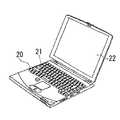
図19は本発明が適用されたノート型パーソナルコンピュータであり、本体20には文字等を入力するとき操作されるキーボード21を含み、本体カバーには画像を表示する表示部22を含み、本発明の表示装置をその表示部22に用いることにより作製される。 FIG. 19 shows a notebook personal computer to which the present invention is applied. The
図20は本発明が適用された携帯端末装置であり、左が開いた状態を表し、右が閉じた状態を表している。この携帯端末装置は、上側筐体23、下側筐体24、連結部(ここではヒンジ部)25、ディスプレイ26、サブディスプレイ27、ピクチャーライト28、カメラ29等を含み、本発明の表示装置をそのディスプレイ26やサブディスプレイ27に用いることにより作製される。 FIG. 20 shows a portable terminal device to which the present invention is applied. The left side shows an open state and the right side shows a closed state. The portable terminal device includes an
図21は本発明が適用されたビデオカメラであり、本体部30、前方を向いた側面に被写体撮影用のレンズ34、撮影時のスタート/ストップスイッチ35、モニター36等を含み、本発明の表示装置をそのモニター36に用いることにより作製される。 FIG. 21 shows a video camera to which the present invention is applied. The video camera includes a
0・・・パネル、1・・・画素アレイ部、2・・・画素回路、3・・・水平セレクタ、4・・・ライトスキャナ、5・・・ドライブスキャナ、71・・・第一補正用スキャナ、72・・・第二補正用スキャナ、Tr1・・・サンプリングトランジスタ、Tr2・・・第1スイッチングトランジスタ、Tr3・・・第2スイッチングトランジスタ、Tr4・・・第3スイッチングトランジスタ、Trd・・・ドライブトランジスタ、Cs・・・保持容量、EL・・・発光素子、Vss1・・・第1電源電位、Vss2・・・第2電源電位、VDD・・・第3電源電位、WS・・・第1走査線、DS・・・第2走査線、AZ1・・・第3走査線、AZ2・・・第4走査線0 ... panel, 1 ... pixel array section, 2 ... pixel circuit, 3 ... horizontal selector, 4 ... light scanner, 5 ... drive scanner, 71 ...
Claims (5)
Translated fromJapanese前記画素アレイ部は、行状の走査線と、列状の信号線と、各走査線と各信号線とが交差する部分に配された行列状の画素とを備え、
各画素は少なくとも、サンプリングトランジスタと、ドライブトランジスタと、保持容量と、発光素子とを備え、
前記サンプリングトランジスタは、その制御端が該走査線に接続し、その一対の電流端が該信号線と該ドライブトランジスタの制御端との間に接続し、
前記ドライブトランジスタは、一対の電流端の一方が該発光素子に接続し、他方が電源に接続し、
前記保持容量は、該ドライブトランジスタの制御端と電流端との間に接続し、
前記駆動部は少なくとも、各走査線に順次制御信号を供給して線順次走査を行うライトスキャナと、各信号線に映像信号を供給する信号セレクタとを有し、
前記サンプリングトランジスタは、該走査線に供給された制御信号に応じてオンし、該信号線から映像信号をサンプリングして該保持容量に書き込むとともに、その間該ドライブトランジスタに流れる電流を該保持容量に負帰還して、該ドライブトランジスタの移動度に対する補正を該保持容量に書き込まれた映像信号にかけ、
前記ドライブトランジスタは、該保持容量に書き込まれた映像信号に応じた電流を該発光素子に供給して発光させる表示装置であって、
前記ライトスキャナは、パルス電源と、シフトレジスタと、出力バッファとを有し、
前記シフトレジスタは、線順次走査に同期してシフトレジスタの各段毎に高電位と低電位の間で遷移する入力信号を順次生成し、
前記パルス電源は、線順次走査に同期して高電位と低電位の間で遷移する電源パルスを逐次生成し、
前記出力バッファは、該シフトレジスタの各段と各走査線との間に接続し、該入力信号に応じて該電源パルスを取り出し制御信号として各走査線に出力し、
前記ライトスキャナは、該電源パルスの低電位よりも該入力信号の低電位が低くなるように電位設定されていることを特徴とする表示装置。It consists of a pixel array part and a drive part,
The pixel array unit includes a row-shaped scanning line, a column-shaped signal line, and a matrix-shaped pixel arranged in a portion where each scanning line and each signal line intersect,
Each pixel includes at least a sampling transistor, a drive transistor, a storage capacitor, and a light emitting element,
The sampling transistor has a control end connected to the scanning line, a pair of current ends connected between the signal line and the control end of the drive transistor,
The drive transistor has one of a pair of current ends connected to the light emitting element, the other connected to a power source,
The storage capacitor is connected between a control terminal and a current terminal of the drive transistor,
The drive unit includes at least a light scanner that sequentially supplies a control signal to each scanning line to perform line sequential scanning, and a signal selector that supplies a video signal to each signal line,
The sampling transistor is turned on in response to a control signal supplied to the scanning line, samples a video signal from the signal line and writes it to the storage capacitor, and at the same time, sinks a current flowing through the drive transistor to the storage capacitor. Feedback, applying a correction for the mobility of the drive transistor to the video signal written in the storage capacitor,
The drive transistor is a display device that emits light by supplying current corresponding to a video signal written in the storage capacitor to the light emitting element,
The write scanner has a pulse power supply, a shift register, and an output buffer,
The shift register sequentially generates an input signal that transitions between a high potential and a low potential for each stage of the shift register in synchronization with line sequential scanning,
The pulse power supply sequentially generates a power supply pulse that transitions between a high potential and a low potential in synchronization with line sequential scanning,
The output buffer is connected between each stage of the shift register and each scanning line, takes out the power pulse in accordance with the input signal, and outputs it as a control signal to each scanning line,
The display device is characterized in that the write scanner is set to a potential so that a low potential of the input signal is lower than a low potential of the power pulse.
該電源パルスの低電位と該入力信号の低電位との差が、該Pチャネルトランジスタの閾電圧を越えるように電位設定することを特徴とする請求項1記載の表示装置。The output buffer includes an inverter composed of a P-channel transistor and an N-channel transistor connected in series between a power supply line to which the power supply pulse is supplied and a predetermined ground line.
2. The display device according to claim 1, wherein the potential is set so that a difference between a low potential of the power supply pulse and a low potential of the input signal exceeds a threshold voltage of the P-channel transistor.
前記出力バッファは、該傾斜の付いた立下り波形を抜き取って、該サンプリングトランジスタがオフするタイミングを規定する該制御信号の立下り波形とし、
前記サンプリングトランジスタは、映像信号のレベルに応じ該制御信号の立下り波形の傾斜に従ってオフするタイミングが変化することを特徴とする請求項1記載の表示装置。The pulse power supply generates a power pulse with a slope in the falling waveform,
The output buffer extracts the falling waveform with the slope and sets the falling waveform of the control signal that defines the timing at which the sampling transistor is turned off,
2. The display device according to claim 1, wherein the timing at which the sampling transistor is turned off changes according to the slope of the falling waveform of the control signal in accordance with the level of the video signal.
前記画素アレイ部は、行状の走査線と、列状の信号線と、各走査線と各信号線とが交差する部分に配された行列状の画素とを備え、
各画素は少なくとも、サンプリングトランジスタと、ドライブトランジスタと、保持容量と、発光素子とを備え、
前記サンプリングトランジスタは、その制御端が該走査線に接続し、その一対の電流端が該信号線と該ドライブトランジスタの制御端との間に接続し、
前記ドライブトランジスタは、一対の電流端の一方が該発光素子に接続し、他方が電源に接続し、
前記保持容量は、該ドライブトランジスタの制御端と電流端との間に接続し、
前記駆動部は少なくとも、各走査線に順次制御信号を供給して線順次走査を行うライトスキャナと、各信号線に映像信号を供給する信号セレクタとを有し、
前記サンプリングトランジスタは、該走査線に供給された制御信号に応じてオンし、該信号線から映像信号をサンプリングして該保持容量に書き込むとともに、その間該ドライブトランジスタに流れる電流を該保持容量に負帰還して、該ドライブトランジスタの移動度に対する補正を該保持容量に書き込まれた映像信号にかけ、
前記ドライブトランジスタは、該保持容量に書き込まれた映像信号に応じた電流を該発光素子に供給して発光させる表示装置の駆動方法であって、
前記ライトスキャナは、パルス電源と、シフトレジスタと、出力バッファとを有し、
線順次走査に同期して該シフトレジスタの各段毎に高電位と低電位の間で遷移する入力信号を順次生成し、
線順次走査に同期して高電位と低電位の間で遷移する電源パルスを該パルス電源から逐次生成し、
該シフトレジスタの各段と各走査線との間に接続した該出力バッファにより、該入力信号に応じて該電源パルスを取り出し制御信号として各走査線に出力し、
該電源パルスの低電位よりも該入力信号の低電位が低くなるように電位設定することを特徴とする表示装置の駆動方法。It consists of a pixel array part and a drive part,
The pixel array unit includes a row-shaped scanning line, a column-shaped signal line, and a matrix-shaped pixel arranged in a portion where each scanning line and each signal line intersect,
Each pixel includes at least a sampling transistor, a drive transistor, a storage capacitor, and a light emitting element,
The sampling transistor has a control end connected to the scanning line, a pair of current ends connected between the signal line and the control end of the drive transistor,
The drive transistor has one of a pair of current ends connected to the light emitting element, the other connected to a power source,
The storage capacitor is connected between a control terminal and a current terminal of the drive transistor,
The drive unit includes at least a light scanner that sequentially supplies a control signal to each scanning line to perform line sequential scanning, and a signal selector that supplies a video signal to each signal line,
The sampling transistor is turned on in response to a control signal supplied to the scanning line, samples a video signal from the signal line and writes it to the storage capacitor, and at the same time, sinks a current flowing through the drive transistor to the storage capacitor. Feedback, applying a correction for the mobility of the drive transistor to the video signal written in the storage capacitor,
The drive transistor is a method for driving a display device that emits light by supplying a current corresponding to a video signal written in the storage capacitor to the light emitting element,
The write scanner has a pulse power supply, a shift register, and an output buffer,
In synchronization with line sequential scanning, an input signal that transitions between a high potential and a low potential is sequentially generated for each stage of the shift register,
A power supply pulse that transitions between a high potential and a low potential in synchronization with line sequential scanning is sequentially generated from the pulse power supply,
The output buffer connected between each stage of the shift register and each scanning line takes out the power pulse in accordance with the input signal and outputs it as a control signal to each scanning line,
A method for driving a display device, characterized in that a potential is set so that a low potential of the input signal is lower than a low potential of the power supply pulse.
Priority Applications (1)
| Application Number | Priority Date | Filing Date | Title |
|---|---|---|---|
| JP2007250574AJP2009080367A (en) | 2007-09-27 | 2007-09-27 | Display device, its driving method, and electronic equipment |
Applications Claiming Priority (1)
| Application Number | Priority Date | Filing Date | Title |
|---|---|---|---|
| JP2007250574AJP2009080367A (en) | 2007-09-27 | 2007-09-27 | Display device, its driving method, and electronic equipment |
Publications (1)
| Publication Number | Publication Date |
|---|---|
| JP2009080367Atrue JP2009080367A (en) | 2009-04-16 |
Family
ID=40655142
Family Applications (1)
| Application Number | Title | Priority Date | Filing Date |
|---|---|---|---|
| JP2007250574AWithdrawnJP2009080367A (en) | 2007-09-27 | 2007-09-27 | Display device, its driving method, and electronic equipment |
Country Status (1)
| Country | Link |
|---|---|
| JP (1) | JP2009080367A (en) |
Cited By (6)
| Publication number | Priority date | Publication date | Assignee | Title |
|---|---|---|---|---|
| JP2010276903A (en)* | 2009-05-29 | 2010-12-09 | Seiko Epson Corp | LIGHT EMITTING DEVICE, LIGHT EMITTING DEVICE DRIVE METHOD, AND ELECTRONIC DEVICE |
| CN103456662A (en)* | 2012-06-01 | 2013-12-18 | 亚威科股份有限公司 | Substrate separation device and method for separating the substrate using thereof |
| KR101521706B1 (en)* | 2012-09-20 | 2015-05-19 | 베이징 비오이 옵토일렉트로닉스 테크놀로지 컴퍼니 리미티드 | Gate driving circuit, array substrate, and display apparatus |
| US10319303B2 (en) | 2016-03-30 | 2019-06-11 | Joled Inc. | Display device for decreasing capacitance voltage dependence |
| US10395595B2 (en) | 2016-06-02 | 2019-08-27 | Joled Inc. | Display device |
| WO2020148604A1 (en)* | 2019-01-18 | 2020-07-23 | 株式会社半導体エネルギー研究所 | Display apparatus and electronic device |
- 2007
- 2007-09-27JPJP2007250574Apatent/JP2009080367A/ennot_activeWithdrawn
Cited By (10)
| Publication number | Priority date | Publication date | Assignee | Title |
|---|---|---|---|---|
| JP2010276903A (en)* | 2009-05-29 | 2010-12-09 | Seiko Epson Corp | LIGHT EMITTING DEVICE, LIGHT EMITTING DEVICE DRIVE METHOD, AND ELECTRONIC DEVICE |
| CN103456662A (en)* | 2012-06-01 | 2013-12-18 | 亚威科股份有限公司 | Substrate separation device and method for separating the substrate using thereof |
| KR101521706B1 (en)* | 2012-09-20 | 2015-05-19 | 베이징 비오이 옵토일렉트로닉스 테크놀로지 컴퍼니 리미티드 | Gate driving circuit, array substrate, and display apparatus |
| US9218780B2 (en) | 2012-09-20 | 2015-12-22 | Beijing Boe Optoelectronics Technology Co., Ltd. | Gate driving circuit, array substrate, and display apparatus |
| US10319303B2 (en) | 2016-03-30 | 2019-06-11 | Joled Inc. | Display device for decreasing capacitance voltage dependence |
| US10395595B2 (en) | 2016-06-02 | 2019-08-27 | Joled Inc. | Display device |
| WO2020148604A1 (en)* | 2019-01-18 | 2020-07-23 | 株式会社半導体エネルギー研究所 | Display apparatus and electronic device |
| JPWO2020148604A1 (en)* | 2019-01-18 | 2020-07-23 | ||
| JP2024050530A (en)* | 2019-01-18 | 2024-04-10 | 株式会社半導体エネルギー研究所 | Display device and electronic device |
| JP7566117B2 (en) | 2019-01-18 | 2024-10-11 | 株式会社半導体エネルギー研究所 | Display device and electronic device |
Similar Documents
| Publication | Publication Date | Title |
|---|---|---|
| JP4715850B2 (en) | Display device, driving method thereof, and electronic apparatus | |
| JP4433039B2 (en) | Display device, driving method thereof, and electronic apparatus | |
| JP4300490B2 (en) | Display device, driving method thereof, and electronic apparatus | |
| JP4297169B2 (en) | Display device, driving method thereof, and electronic apparatus | |
| KR101414127B1 (en) | DISPLAY DEVICE, METHOD OF DRIVING THE SAME, | |
| CN101312012B (en) | Display device, driving method thereof, and electronic device | |
| JP4534169B2 (en) | Display device, driving method thereof, and electronic apparatus | |
| JP2008287139A (en) | Display device, driving method thereof, and electronic apparatus | |
| JP2008233651A (en) | Display device and driving method thereof, and electronic equipment | |
| JP2007156460A (en) | Display device and driving method thereof | |
| JP5082532B2 (en) | Display device, driving method thereof, and electronic apparatus | |
| JP4591511B2 (en) | Display device and electronic device | |
| JP4534170B2 (en) | Display device, driving method thereof, and electronic apparatus | |
| CN100594535C (en) | Display device, driving method thereof, and electronic device | |
| JP2008241780A (en) | Display device and electronic equipment | |
| JP2009080367A (en) | Display device, its driving method, and electronic equipment | |
| JP2008197607A (en) | Pixel circuit, image display device and its driving method | |
| JP2008203661A (en) | Image display and its driving method | |
| JP2008287140A (en) | Display device and electronic equipment | |
| JP2009098430A (en) | Display device and electronic apparatus | |
| JP2009098429A (en) | Display device and electronic apparatus | |
| JP2010122604A (en) | Display device and electronic equipment | |
| JP2009098431A (en) | Display device and electronic apparatus |
Legal Events
| Date | Code | Title | Description |
|---|---|---|---|
| RD02 | Notification of acceptance of power of attorney | Free format text:JAPANESE INTERMEDIATE CODE: A7422 Effective date:20090212 | |
| RD05 | Notification of revocation of power of attorney | Free format text:JAPANESE INTERMEDIATE CODE: A7425 Effective date:20090226 | |
| A300 | Application deemed to be withdrawn because no request for examination was validly filed | Free format text:JAPANESE INTERMEDIATE CODE: A300 Effective date:20101207 |