JP2009076237A - EL light-emitting touch switch - Google Patents
EL light-emitting touch switchDownload PDFInfo
- Publication number
- JP2009076237A JP2009076237AJP2007242059AJP2007242059AJP2009076237AJP 2009076237 AJP2009076237 AJP 2009076237AJP 2007242059 AJP2007242059 AJP 2007242059AJP 2007242059 AJP2007242059 AJP 2007242059AJP 2009076237 AJP2009076237 AJP 2009076237A
- Authority
- JP
- Japan
- Prior art keywords
- electrode
- light
- touch switch
- touch
- light emitting
- Prior art date
- Legal status (The legal status is an assumption and is not a legal conclusion. Google has not performed a legal analysis and makes no representation as to the accuracy of the status listed.)
- Granted
Links
Images


Classifications
- H—ELECTRICITY
- H01—ELECTRIC ELEMENTS
- H01H—ELECTRIC SWITCHES; RELAYS; SELECTORS; EMERGENCY PROTECTIVE DEVICES
- H01H13/00—Switches having rectilinearly-movable operating part or parts adapted for pushing or pulling in one direction only, e.g. push-button switch
- H01H13/70—Switches having rectilinearly-movable operating part or parts adapted for pushing or pulling in one direction only, e.g. push-button switch having a plurality of operating members associated with different sets of contacts, e.g. keyboard
- H01H13/702—Switches having rectilinearly-movable operating part or parts adapted for pushing or pulling in one direction only, e.g. push-button switch having a plurality of operating members associated with different sets of contacts, e.g. keyboard with contacts carried by or formed from layers in a multilayer structure, e.g. membrane switches
- H—ELECTRICITY
- H03—ELECTRONIC CIRCUITRY
- H03K—PULSE TECHNIQUE
- H03K17/00—Electronic switching or gating, i.e. not by contact-making and –breaking
- H03K17/94—Electronic switching or gating, i.e. not by contact-making and –breaking characterised by the way in which the control signals are generated
- H03K17/96—Touch switches
- H03K17/962—Capacitive touch switches
- H03K17/9622—Capacitive touch switches using a plurality of detectors, e.g. keyboard
- H—ELECTRICITY
- H01—ELECTRIC ELEMENTS
- H01H—ELECTRIC SWITCHES; RELAYS; SELECTORS; EMERGENCY PROTECTIVE DEVICES
- H01H36/00—Switches actuated by change of magnetic field or of electric field, e.g. by change of relative position of magnet and switch, by shielding
- H—ELECTRICITY
- H03—ELECTRONIC CIRCUITRY
- H03K—PULSE TECHNIQUE
- H03K2217/00—Indexing scheme related to electronic switching or gating, i.e. not by contact-making or -breaking covered by H03K17/00
- H03K2217/94—Indexing scheme related to electronic switching or gating, i.e. not by contact-making or -breaking covered by H03K17/00 characterised by the way in which the control signal is generated
- H03K2217/96—Touch switches
- H03K2217/9607—Capacitive touch switches
- H03K2217/960785—Capacitive touch switches with illumination
Landscapes
- Switches That Are Operated By Magnetic Or Electric Fields (AREA)
- Electronic Switches (AREA)
- Electroluminescent Light Sources (AREA)
- Push-Button Switches (AREA)
- Circuit Arrangement For Electric Light Sources In General (AREA)
- Control Of El Displays (AREA)
Abstract
Description
Translated fromJapanese本発明は、EL(エレクトロルミネッセンス)とタッチスイッチとを組み合わせたEL発光式タッチスイッチに係り、特に、複数のタッチ検出電極を備えたEL発光式タッチスイッチに関する。 The present invention relates to an EL light emitting touch switch in which an EL (electroluminescence) and a touch switch are combined, and more particularly to an EL light emitting touch switch including a plurality of touch detection electrodes.
従来から、導電性の電極部材に人体の一部が接触または近接するとこれを検出するタッチスイッチが知られている。このようなタッチスイッチでは、電極部材が静電容量センサとして機能するものであって、人体が電極にふれた際の電極のインピーダンス(静電容量)の変化に基づいて、タッチスイッチのオンオフを検出するようになっている。
更に、このようなタッチスイッチに、蛍光体から光を放出する有機または無機のEL素子を組み合わせ、人体の接触を検出する電極部が発光可能なものが知られている(特許文献1)。Conventionally, a touch switch that detects when a part of a human body contacts or approaches a conductive electrode member is known. In such a touch switch, the electrode member functions as a capacitance sensor, and on / off of the touch switch is detected based on a change in impedance (capacitance) of the electrode when a human body touches the electrode. It is supposed to be.
Furthermore, there is known a touch switch that is combined with an organic or inorganic EL element that emits light from a phosphor, and an electrode portion that detects contact with a human body can emit light (Patent Document 1).
図3はこのようなタッチスイッチの本体部の構造を示す模式的な断面図の一例である。
図3に示すように、タッチスイッチ本体部には、透明絶縁基板2の表面(上面)に透明電極5が設けられ、更にその上面が透明絶縁被膜6で覆われてタッチ面が形成されている。
また、透明絶縁基板2の裏面(下面)にはEL発光層1が形成されている。このEL発光層1は、透明絶縁基板2側から下方へ順に、透明電極1a、蛍光層1b、絶縁層1c、背面電極1dを積層して形成されており、2つの電極1a、1d間に交流電圧を印加することによってEL発光層1を発光させている。FIG. 3 is an example of a schematic cross-sectional view showing the structure of the main body of such a touch switch.
As shown in FIG. 3, in the touch switch main body, a transparent electrode 5 is provided on the surface (upper surface) of the
An EL
この発光は、透明電極1a、透明絶縁基板2、タッチ検出用の透明電極5及び透明絶縁被膜6を介して外部に到達するので、オペレータ(操作者)はこの発光を頼りに透明絶縁被膜2を容易に指先で触れることができる。そして、透明絶縁被膜6に指先が触れることで、検出用の透明電極5と接続した図示しないタッチ判定回路が、インピーダンス変化や容量変化を検知し、タッチされたことを判定するとともに、これに接続された機器のオンオフ制御を実行可能としている。 Since this light emission reaches the outside through the transparent electrode 1a, the transparent
しかしながら、このようなタッチスイッチでは、EL発光層1を発光駆動させるための1対の電極1a、1dと、タッチ検出用の透明電極5とが必要となるため、スイッチの薄型が困難であるとともに、積層する各電極の層数が増加してコストアップとなっていた。
そこで、このような課題を解決するべく、特許文献2には、タッチ検出用の電極とEL駆動用の電極を共用させて、スイッチの薄型化を可能としたEL発光式タッチスイッチが開示されている。However, in such a touch switch, a pair of
Therefore, in order to solve such problems,
図4は、特許文献2に開示されたEL発光式タッチスイッチの概略構成図である。図4に示すように、タッチスイッチ本体部10は、透明電極(表面電極)1aと背面電極1dとの間に蛍光層1bと絶縁層1cとを積層して構成されるEL発光層1を備え、絶縁基板3の上にEL発光層1が形成され、更にその上に透明絶縁被膜6を形成して構成されている。ここで、透明電極1aは、タッチ検出用の電極としての機能とEL駆動用の電極としての機能とを兼ね備えている。 FIG. 4 is a schematic configuration diagram of an EL light-emitting touch switch disclosed in
また、このタッチスイッチ本体部10には、透明電極1aの電位の変化を検知して透明絶縁被膜6に対するオペレータの接触を検知するタッチ判定回路100と、EL発光層1を発光させるべく透明電極1aの電位を基準とした交流電圧を出力するEL駆動回路200とが並列に接続されている。
また、該タッチ判定回路100と該EL駆動回路200に加えてさらに駆動制御回路300が設けられており、この駆動制御回路300からの制御信号により、タッチ判定回路100が作動するようになっている。そして、該タッチ判定回路100では、透明電極1aの電位VAと設置電位VGとの電位差の変化から透明絶縁被膜6に対する指の接触を検知するように構成されており、該タッチ判定回路100においてタッチ判定されると、EL駆動回路200をオンオフ駆動させて上記両電極1a、1d間に交流電界を印加し、EL発光層1の発光を制御するように構成されている。
In addition to the
ところで、このようなタッチスイッチを自動車の車室内の機器(具体的には、自動車のオーディオやエアコンディショナ)の操作パネル用に適用することが考えられる。
しかしながら、上記特許文献1に開示された技術では、薄型化が困難であり、例えば自動車のオーディオやエアコンディショナの操作パネルとしては適したものではない。また、特許文献2に開示された技術では、タッチ検出電極(透明電極1a)が1つの場合には問題ないが、自動車用機器の操作パネルのように、タッチ検出電極が同一パネル内に複数存在する場合には、有効な解決手段とはなり得ない。By the way, it can be considered that such a touch switch is applied to an operation panel of a device in a vehicle interior of a vehicle (specifically, an audio device or an air conditioner of a vehicle).
However, the technique disclosed in
つまり、多くの独立した発光部位(EL発光層1)を備えるELパネルにおいては、背面電極1dは、発光部位全体を覆う面積で形成し、共通電極とするのが一般的である。
しかし、このような構成のELパネルにおいて、特許文献2に開示されているように、タッチ検出電極と兼用した透明電極1aを基準にEL駆動回路を接続する、即ち背面電極1dは接地電位に対してフローティングであるが如く構成した場合は、独立した発光部位である透明電極1aと背面電極1dとの間には大きな静電容量が存在するため、複数のタッチ検出電極のいずれかを触ると、同時に全てのスイッチに於いてタッチを検出してしまうことになる(図5参照)。That is, in an EL panel including many independent light emitting parts (EL light emitting layer 1), the
However, in the EL panel having such a configuration, as disclosed in
本発明はこのような問題点を解決するためになされたもので、その目的とするところは、タッチ検出用の電極としての機能とEL駆動用の電極としての機能とを兼ね備えた複数の表面電極と、単一の(共通の)背面電極とを備えたEL発光式タッチスイッチにおいて、相互の表面電極の影響を排除して、各表面電極が独立して正確にタッチ判定できるようにした、EL発光式タッチスイッチを提供することを目的とする。 The present invention has been made in order to solve such problems, and the object of the present invention is to provide a plurality of surface electrodes having a function as an electrode for touch detection and a function as an electrode for EL driving. In addition, in an EL light emitting touch switch having a single (common) back electrode, each surface electrode can accurately and independently perform touch determination by eliminating the influence of each surface electrode. An object is to provide a light-emitting touch switch.
上記の目的を達成するために、請求項1の発明は、透光性を有する複数の第1電極と、複数の第1電極と対向して配置され、複数の第1電極に対して単一の電極として設けられた第2電極と、第1電極と第2電極との間に夫々設けられ、蛍光層及び絶縁層を積層して形成されたEL発光層と、EL発光層が発光するように、第1電極と第2電極との間に駆動電圧を印加する発光駆動手段と、駆動電圧の印加が所定周期で停止するように、発光駆動手段を制御するタイミング信号を発生するタイミング信号発生手段と、第1電極と第2電極との電位が一致するように第1の電極に電流を供給する帰還回路を有し、タイミング信号に基づいて発光駆動手段における駆動電圧の印加が停止しているときに、前記帰還回路の作動に基づいて第1の電極への人体の接触を判定するタッチ判定手段と、を備えてEL発光式タッチスイッチを構成することを特徴とする。 In order to achieve the above-mentioned object, the invention of
また、請求項2の発明は、請求項1において、帰還回路は、オペアンプと抵抗とを含んで構成される差動増幅回路であって、タッチ判定手段は、オペアンプの出力電圧に基づいて第1の電極への人体の接触を判定することを特徴とする。 According to a second aspect of the present invention, in the first aspect, the feedback circuit is a differential amplifier circuit including an operational amplifier and a resistor, and the touch determination means is a first circuit based on the output voltage of the operational amplifier. The contact of the human body with the electrode is determined.
本発明の請求項1のEL発光式タッチスイッチによれば、第1電極がタッチ検出用の電極としての機能とEL駆動用の電極としての機能とを兼ね備えた表面電極として、第2電極が単一の(共通の)背面電極として、複数の表面電極を有するEL発光式タッチスイッチが得られ、該表面電極と背面電極との間に介在する静電容量によって発生する相互の表面電極の影響を排除することができ、表面電極のタッチ判定を正確に行うことができる。したがって、例えば自動車の車室内の機器の操作パネル(インストルメンタルパネル)のように、複数のスイッチが設けられるパネルに最適なEL発光式タッチスイッチを得ることができる。 According to the EL light emission type touch switch of the first aspect of the present invention, the first electrode is a surface electrode having both a function as an electrode for touch detection and a function as an electrode for EL drive, and the second electrode is a single electrode. An EL light emitting touch switch having a plurality of surface electrodes is obtained as one (common) back electrode, and the influence of the mutual surface electrodes generated by the capacitance interposed between the surface electrode and the back electrode is obtained. Therefore, it is possible to accurately perform the touch determination on the surface electrode. Therefore, it is possible to obtain an EL light-emitting touch switch that is optimal for a panel provided with a plurality of switches, such as an operation panel (instrumental panel) of equipment in a vehicle interior of an automobile.
また、本発明の請求項2のEL発光式タッチスイッチによれば、簡単な構成で、第1電極と第2電極との電位が一致するように第1電極に電流が供給され、タッチ判定手段を容易に実現することができる。 According to the EL light emission type touch switch of the second aspect of the present invention, the current is supplied to the first electrode so that the potentials of the first electrode and the second electrode coincide with each other with a simple configuration. Can be easily realized.
以下、図面に基づき本発明の実施形態について説明する。
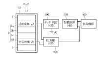
図1は、本発明のEL発光式タッチスイッチのシステム構成図である。
図1に示すように、本実施形態のEL発光式タッチスイッチは、タッチスイッチ本体部10と、EL駆動手段20(発光駆動手段)と、タイミング信号発生手段30と、検出手段40(タッチ判定手段)とを備えて構成されている。Hereinafter, embodiments of the present invention will be described with reference to the drawings.
FIG. 1 is a system configuration diagram of an EL light emitting touch switch according to the present invention.
As shown in FIG. 1, the EL light emission type touch switch of the present embodiment includes a touch switch
タッチスイッチ本体部10は、図4に示す従来のタッチスイッチ本体部10と同様に、表面電極(透明電極)1a(第1電極)と背面電極1d(第2電極)との間に蛍光層1bと絶縁層1cとを積層して構成されるEL発光層1を備え、更にその上に透明絶縁被膜6を形成して構成されており、表面電極1aはタッチ検出用の電極とEL駆動用の電極を共用させた構造となっている。本実施形態のタッチスイッチ本体部10は、複数のタッチ検出用の電極を備えたパネル状に形成されており、1つの背面電極1dに対して複数の表面電極1aが備えられている。また、これに伴い、各表面電極1a毎にEL発光層1が夫々形成されている。 As with the conventional
EL駆動手段20は、例えば200V/5kHzの正弦波出力の交流電源21と、スイッチング手段22とを備えており、各EL発光層1を発光させるために、背面電極1dと各表面電極1aとの間に駆動用電圧を印加する機能を有している。
スイッチング手段22は、交流電源21と各表面電極1aとを接続する回路に夫々介装され、該回路の連通遮断を切り換える機能を有する。EL駆動手段20は、図示しない外部要件(例えば、車両における夜間照明用スイッチが操作された場合)に応じて、該当するEL発光層に対応する表面電極1aと接続されたスイッチング手段22をオンオフする。更に、スイッチング手段22は、タイミング信号発生手段30により供給される周期的なタイミング信号T1によっても、その開閉作動が制御される。したがって、スイッチング手段22は、外部要件に応じてON制御されている期間において、タイミング信号T1に合わせて周期的にオンオフ作動する。The EL driving means 20 includes, for example, an
The
検出手段40は、各表面電極1a毎に夫々設けられ、表面電極1aに人体が接触したか否かを検出する機能を有している。詳しくは、検出手段40は、表面電極1aから入力する入力信号(入力電圧)S2と、背面電極1dから入力する入力信号(入力電圧)S1とに基づいて人体の接触を判定するものであって、抵抗R1〜R4及びオペアンプ41からなる差動増幅回路(帰還回路)と判定回路42とを含んで構成されており、該抵抗R1〜R4の抵抗値は以下の(1)及び(2)式のように設定されている。
R1=R2・・・(1)
R3=R4・・・(2)
上記スイッチング手段22がON作動してEL発光層が発光している場合には、該スイッチング手段22のON作動によって、S2入力側が接地され、S1入力側にのみ交流電源21の電圧が印加される。The detection means 40 is provided for each surface electrode 1a, and has a function of detecting whether or not a human body contacts the surface electrode 1a. Specifically, the detection means 40 determines contact of a human body based on an input signal (input voltage) S2 input from the surface electrode 1a and an input signal (input voltage) S1 input from the
R1 = R2 (1)
R3 = R4 (2)
When the switching means 22 is turned on and the EL light emitting layer emits light, the switching means 22 is turned on, the S2 input side is grounded, and the voltage of the
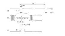
図2は、タイミング信号T1、T2、差動増幅回路出力信号(オペアンプ41の出力信号)S3の推移を示すタイムチャートである。交流電源21による電圧の印加により、オペアンプ41の出力信号(出力電圧)S3は図2に示す如く、交流電源21の電圧に対応して大きな振幅を有し、その値は以下の(3)式に表される。
S3=(S2−S1)R3/R1・・・(3)
タイミング信号発生手段30は、タイミング信号T1として、周期taで時間tbの間OFFとなるL信号を出力し、かかるL信号の出力時(OFF時)に該スイッチング手段22がOFF(断)作動するように設定されている。好ましくは、周期taが50msec程度に、時間tbが2msec程度に設定すればよいが、これらの値に限定されるものではなく、tb<taとなるように設定すればよい。また、タイミング信号発生手段30は、タイミング信号T2として、時間tbより短いH信号を判定回路42に出力する。H信号の発生開始(OFFからONに切り換わる)タイミングは、L信号出力期間中になるように設定されている。FIG. 2 is a time chart showing transitions of the timing signals T1, T2 and the differential amplifier circuit output signal (output signal of the operational amplifier 41) S3. By applying a voltage from the
S3 = (S2-S1) R3 / R1 (3)
The timing signal generating means 30 outputs an L signal that is OFF for a time tb with a period ta as the timing signal T1, and the switching means 22 is turned OFF when the L signal is output (when OFF). Is set to Preferably, the period ta may be set to about 50 msec and the time tb may be set to about 2 msec, but is not limited to these values, and may be set to satisfy tb <ta. Further, the timing signal generating means 30 outputs an H signal shorter than the time tb to the
L信号の出力時(OFF時)において、タッチスイッチ本体部10における背面電極1dと表面電極1aとの間は大きな静電容量で結合されているので、背面電極1d及び表面電極1aは、ともに交流電源21の電圧と等しくなる。したがって、差動増幅回路の出力信号S3は、スイッチング手段22のOFF作動中は0Vとなる。
ここで、オペレータによって、表面電極1aに触れると、該オペレータを介して接地電流ISが流れる。これにより、表面電極1a側の電位が下がろうとして入力信号S1とS2との間に電位差が発生する。ところが、オペアンプ41は、該電位差を打ち消すが如く抵抗R3を介して帰還電流Ifを発生する(オペアンプ回路のイマジナリーショート状態を示す)ので、結果的にS1とS2、言い換えれば背面電極1dと表面電極1aとの電位差は打ち消されることとなる。したがって、このときオペアンプ41から抵抗R3を介して帰還電流を流す為に発生する電圧である出力信号S3は、オペレータを介して流れた接地電流ISに比例することとなる。When the L signal is output (OFF), the
Here, when the operator touches the surface electrode 1a, the ground current IS flows through the operator. As a result, a potential difference is generated between the input signals S1 and S2 in an attempt to lower the potential on the surface electrode 1a side. However, the
上記のように作用することで、出力信号S3は、スイッチング手段22のOFF期間中に、表面電極1aに対してオペレータが触れたか否かによって、図2の実線と破線で示す如く振幅が変化する。そして、この振幅の変化に基づいて判定回路42は、オペレータの操作を検出する。
判定回路42は、出力信号S3の振幅を電圧に置き換える図示しない検波回路を備えており、該電圧と所定の閾値とをタイミング信号発生手段30から供給されたタイミング信号T2の立ち上がりタイミングで比較する。そして、該比較の結果を端子S4から出力して、各検出手段40に接続された車両の各機器の作動を制御する。By acting as described above, the amplitude of the output signal S3 changes as shown by the solid line and the broken line in FIG. 2 depending on whether or not the operator touches the surface electrode 1a during the OFF period of the switching means 22. . Based on this change in amplitude, the
The
以上のような構成により、本実施形態では、L信号出力時においてはS1とS2の電位は帰還電流Ifによって等しく保たれる。加えて、抵抗R1=R2、R3=R4であるから結果的に背面電極1dと表面電極1aとの電位も等しくなる。したがって、背面電極1dと表面電極1aとの間に介在する静電容量/又はインピーダンスが如何なる値であったとしても、背面電極1dと表面電極1aとの間に電流が流れることはないので、該静電容量/又はインピーダンスの値はオペレータが表面電極1aに触れたことによって変化する出力信号S3の大きさと関連がない。即ち、該静電容量/又はインピーダンスの値はオペレータが触れたことを検出する場合の検出感度に影響を及ぼさないばかりか、該静電容量/又はインピーダンスによってタッチスイッチ本体部10の隣接する各表面電極1aの相互影響をゼロにすることが可能になるのである。 With the configuration as described above, in the present embodiment, the potentials of S1 and S2 are kept equal by the feedback current If when the L signal is output. In addition, since the resistances R1 = R2 and R3 = R4, the potentials of the
以上のように、本実施形態のEL発光式タッチスイッチは、タッチ検出用の電極としての機能とEL駆動用の電極としての機能とを兼ね備えた複数の表面電極1aと、単一の(共通の)背面電極1bとを備え、表面電極1aと背面電極1bとの間に介在する静電容量によって発生する相互の表面電極の影響を排除することができ、表面電極1aのタッチ判定を正確に行うことができる。 As described above, the EL light emission type touch switch according to the present embodiment includes a plurality of surface electrodes 1a having a function as an electrode for touch detection and a function as an electrode for EL driving, and a single (common) ) The back electrode 1b is provided, and the influence of the mutual surface electrode generated by the capacitance interposed between the surface electrode 1a and the back electrode 1b can be eliminated, and the touch determination of the surface electrode 1a is accurately performed. be able to.
1 EL発光層
1a 表面電極
1d 背面電極
10 タッチスイッチ本体部
20 EL駆動手段
30 タイミング信号発生手段
40 検出手段
41 オペアンプ
R1、R2、R3、R4 抵抗DESCRIPTION OF
Claims (2)
Translated fromJapanese前記第1電極と対向して配置され、前記複数の第1電極に対して単一の電極として設けられた第2電極と、
前記第1電極と第2電極との間に夫々設けられ、蛍光層及び絶縁層を積層して形成されたEL発光層と、
前記EL発光層が発光するように、前記第1電極と第2電極との間に駆動電圧を印加する発光駆動手段と、
前記駆動電圧の印加が所定周期で停止するように、前記発光駆動手段を制御するタイミング信号を発生するタイミング信号発生手段と、
前記第1電極と第2電極との電位が一致するように前記第1電極に電流を供給する帰還回路を有し、前記タイミング信号に基づいて前記発光駆動手段における前記駆動電圧の印加が停止しているときに、前記帰還回路の作動に基づいて前記第1の電極への人体の接触を判定するタッチ判定手段と、
を備えたことを特徴とするEL発光式タッチスイッチ。A plurality of first electrodes having translucency;
A second electrode disposed as opposed to the first electrode and provided as a single electrode with respect to the plurality of first electrodes;
An EL light-emitting layer provided between the first electrode and the second electrode, and formed by laminating a fluorescent layer and an insulating layer;
Light emission driving means for applying a driving voltage between the first electrode and the second electrode so that the EL light emitting layer emits light;
Timing signal generating means for generating a timing signal for controlling the light emission driving means so that application of the driving voltage stops at a predetermined period;
A feedback circuit for supplying a current to the first electrode so that the potentials of the first electrode and the second electrode coincide with each other, and the application of the driving voltage in the light emission driving means is stopped based on the timing signal; Touch determining means for determining contact of the human body with the first electrode based on the operation of the feedback circuit,
An EL light-emitting touch switch comprising:
前記タッチ判定手段は、前記オペアンプの出力電圧に基づいて前記第1の電極への人体の接触を判定することを特徴とする請求項1に記載のEL発光式タッチスイッチ。The feedback circuit is a differential amplifier circuit including an operational amplifier and a resistor,
The EL light-emitting touch switch according to claim 1, wherein the touch determination unit determines contact of a human body with the first electrode based on an output voltage of the operational amplifier.
Priority Applications (6)
| Application Number | Priority Date | Filing Date | Title |
|---|---|---|---|
| JP2007242059AJP4791427B2 (en) | 2007-09-19 | 2007-09-19 | EL light-emitting touch switch |
| US12/076,207US8766924B2 (en) | 2007-09-19 | 2008-03-14 | EL emitting touch switch |
| EP08005164.2AEP2040380B8 (en) | 2007-09-19 | 2008-03-19 | EL emitting touch switch |
| KR1020080030101AKR100992278B1 (en) | 2007-09-19 | 2008-04-01 | EL light-emitting touch switch |
| RU2008125131/09ARU2389132C2 (en) | 2007-09-19 | 2008-06-20 | Sensor switch of electric luminescent radiation |
| CN2008101252540ACN101394175B (en) | 2007-09-19 | 2008-06-23 | El emitting touch switch |
Applications Claiming Priority (1)
| Application Number | Priority Date | Filing Date | Title |
|---|---|---|---|
| JP2007242059AJP4791427B2 (en) | 2007-09-19 | 2007-09-19 | EL light-emitting touch switch |
Publications (2)
| Publication Number | Publication Date |
|---|---|
| JP2009076237Atrue JP2009076237A (en) | 2009-04-09 |
| JP4791427B2 JP4791427B2 (en) | 2011-10-12 |
Family
ID=40242717
Family Applications (1)
| Application Number | Title | Priority Date | Filing Date |
|---|---|---|---|
| JP2007242059AExpired - Fee RelatedJP4791427B2 (en) | 2007-09-19 | 2007-09-19 | EL light-emitting touch switch |
Country Status (6)
| Country | Link |
|---|---|
| US (1) | US8766924B2 (en) |
| EP (1) | EP2040380B8 (en) |
| JP (1) | JP4791427B2 (en) |
| KR (1) | KR100992278B1 (en) |
| CN (1) | CN101394175B (en) |
| RU (1) | RU2389132C2 (en) |
Cited By (5)
| Publication number | Priority date | Publication date | Assignee | Title |
|---|---|---|---|---|
| KR101202745B1 (en) | 2011-04-21 | 2012-11-19 | 주식회사 실리콘웍스 | Touch sensing circuit |
| JP2013235313A (en)* | 2012-05-07 | 2013-11-21 | Takuo Takai | Input device for touch switch |
| WO2015186266A1 (en)* | 2014-06-06 | 2015-12-10 | コニカミノルタ株式会社 | Organic electroluminescence module, smart device, and illumination device |
| WO2016031593A1 (en)* | 2014-08-25 | 2016-03-03 | コニカミノルタ株式会社 | Organic electroluminescent module, smart device, and illumination apparatus |
| WO2016181704A1 (en)* | 2015-05-13 | 2016-11-17 | コニカミノルタ株式会社 | Organic electroluminescence module and smart device |
Families Citing this family (5)
| Publication number | Priority date | Publication date | Assignee | Title |
|---|---|---|---|---|
| JP5548270B2 (en)* | 2009-08-21 | 2014-07-16 | アップル インコーポレイテッド | Capacitive sensing method and apparatus |
| KR101649626B1 (en)* | 2009-08-27 | 2016-08-19 | 엘지전자 주식회사 | Mobile terminal |
| KR101588450B1 (en)* | 2009-10-23 | 2016-01-25 | 엘지디스플레이 주식회사 | Touch sensor in-cell type organic electroluminescent device and methode of fabricating the same |
| JP5766928B2 (en)* | 2010-09-29 | 2015-08-19 | 株式会社ジャパンディスプレイ | Display device with touch detection function and electronic device |
| US9035894B2 (en)* | 2013-01-24 | 2015-05-19 | Industrial Technology Research Institute | Touch sensing and feedback apparatuses and methods |
Citations (7)
| Publication number | Priority date | Publication date | Assignee | Title |
|---|---|---|---|---|
| JPS54134377A (en)* | 1978-04-11 | 1979-10-18 | Hitachi Ltd | Display element drive circuit |
| JPS5528247A (en)* | 1978-08-21 | 1980-02-28 | Hitachi Ltd | El element drive circuit |
| GB2059657A (en)* | 1977-07-30 | 1981-04-23 | Ti Group Services Ltd | Supervision of touch control switches |
| JPH03284259A (en)* | 1990-03-30 | 1991-12-13 | Shimadzu Corp | Patient transfer apparatus |
| JP2000150144A (en)* | 1998-11-11 | 2000-05-30 | Citizen Electronics Co Ltd | El inverter using simulated inductor |
| JP2003075547A (en)* | 2001-09-04 | 2003-03-12 | Matsushita Electric Ind Co Ltd | Object detection device |
| JP2005166939A (en)* | 2003-12-02 | 2005-06-23 | Sumitomo Electric Ind Ltd | Semiconductor light emitting device driving circuit |
Family Cites Families (15)
| Publication number | Priority date | Publication date | Assignee | Title |
|---|---|---|---|---|
| DE2626927B2 (en)* | 1976-06-16 | 1981-02-19 | Bodenseewerk Perkin-Elmer & Co Gmbh, 7770 Ueberlingen | Circuit for converting an alternating voltage into a direct voltage |
| US4740781A (en)* | 1985-02-08 | 1988-04-26 | Itt Gilfillan | Touch panel data entry device for thin film electroluminescent panels |
| JPH05135654A (en) | 1991-11-14 | 1993-06-01 | Matsushita Electric Ind Co Ltd | EL illuminated switch |
| US5572205A (en)* | 1993-03-29 | 1996-11-05 | Donnelly Technology, Inc. | Touch control system |
| KR100300397B1 (en) | 1994-04-21 | 2001-10-22 | 김순택 | System having touch panel and digitizer function and driving method |
| JP3284259B2 (en) | 1996-03-14 | 2002-05-20 | 松下電工株式会社 | EL illuminated touch switch |
| JP3473303B2 (en)* | 1996-12-24 | 2003-12-02 | 松下電工株式会社 | Illuminated touch switch device |
| JP3394187B2 (en)* | 1997-08-08 | 2003-04-07 | シャープ株式会社 | Coordinate input device and display integrated type coordinate input device |
| TW507158B (en)* | 2001-01-05 | 2002-10-21 | Darfon Electronics Corp | Detecting device and method of mouse touch pad |
| CN1275131C (en)* | 2001-08-22 | 2006-09-13 | 夏普株式会社 | Touch sensor, display device with touch sensor and position data generation method |
| KR100449745B1 (en)* | 2002-11-21 | 2004-09-22 | 삼성전자주식회사 | Apparatus and Method for avoiding noise of touch screen |
| US7626575B2 (en)* | 2003-03-28 | 2009-12-01 | Samsung Electronics Co., Ltd. | Light pen |
| US7221359B2 (en)* | 2004-03-17 | 2007-05-22 | Lear Corporation | Illuminated touch switch |
| KR100460194B1 (en)* | 2004-07-22 | 2004-12-04 | (주)디지텍시스템스 | Device for controlling touch panel |
| JP2006313709A (en)* | 2005-05-09 | 2006-11-16 | Hosiden Corp | El illumination type switch |
- 2007
- 2007-09-19JPJP2007242059Apatent/JP4791427B2/ennot_activeExpired - Fee Related
- 2008
- 2008-03-14USUS12/076,207patent/US8766924B2/ennot_activeExpired - Fee Related
- 2008-03-19EPEP08005164.2Apatent/EP2040380B8/ennot_activeCeased
- 2008-04-01KRKR1020080030101Apatent/KR100992278B1/ennot_activeExpired - Fee Related
- 2008-06-20RURU2008125131/09Apatent/RU2389132C2/enactive
- 2008-06-23CNCN2008101252540Apatent/CN101394175B/ennot_activeExpired - Fee Related
Patent Citations (7)
| Publication number | Priority date | Publication date | Assignee | Title |
|---|---|---|---|---|
| GB2059657A (en)* | 1977-07-30 | 1981-04-23 | Ti Group Services Ltd | Supervision of touch control switches |
| JPS54134377A (en)* | 1978-04-11 | 1979-10-18 | Hitachi Ltd | Display element drive circuit |
| JPS5528247A (en)* | 1978-08-21 | 1980-02-28 | Hitachi Ltd | El element drive circuit |
| JPH03284259A (en)* | 1990-03-30 | 1991-12-13 | Shimadzu Corp | Patient transfer apparatus |
| JP2000150144A (en)* | 1998-11-11 | 2000-05-30 | Citizen Electronics Co Ltd | El inverter using simulated inductor |
| JP2003075547A (en)* | 2001-09-04 | 2003-03-12 | Matsushita Electric Ind Co Ltd | Object detection device |
| JP2005166939A (en)* | 2003-12-02 | 2005-06-23 | Sumitomo Electric Ind Ltd | Semiconductor light emitting device driving circuit |
Cited By (7)
| Publication number | Priority date | Publication date | Assignee | Title |
|---|---|---|---|---|
| KR101202745B1 (en) | 2011-04-21 | 2012-11-19 | 주식회사 실리콘웍스 | Touch sensing circuit |
| US8841927B2 (en) | 2011-04-21 | 2014-09-23 | Silicon Works Co., Ltd. | Touch sensing circuit |
| JP2013235313A (en)* | 2012-05-07 | 2013-11-21 | Takuo Takai | Input device for touch switch |
| WO2015186266A1 (en)* | 2014-06-06 | 2015-12-10 | コニカミノルタ株式会社 | Organic electroluminescence module, smart device, and illumination device |
| JPWO2015186266A1 (en)* | 2014-06-06 | 2017-04-20 | コニカミノルタ株式会社 | Organic electroluminescence module, smart device and lighting device |
| WO2016031593A1 (en)* | 2014-08-25 | 2016-03-03 | コニカミノルタ株式会社 | Organic electroluminescent module, smart device, and illumination apparatus |
| WO2016181704A1 (en)* | 2015-05-13 | 2016-11-17 | コニカミノルタ株式会社 | Organic electroluminescence module and smart device |
Also Published As
| Publication number | Publication date |
|---|---|
| KR20090030194A (en) | 2009-03-24 |
| RU2008125131A (en) | 2009-12-27 |
| CN101394175B (en) | 2012-01-18 |
| EP2040380B1 (en) | 2018-10-10 |
| EP2040380A2 (en) | 2009-03-25 |
| EP2040380A3 (en) | 2014-11-26 |
| US20090073133A1 (en) | 2009-03-19 |
| KR100992278B1 (en) | 2010-11-05 |
| EP2040380B8 (en) | 2019-03-06 |
| US8766924B2 (en) | 2014-07-01 |
| RU2389132C2 (en) | 2010-05-10 |
| CN101394175A (en) | 2009-03-25 |
| JP4791427B2 (en) | 2011-10-12 |
Similar Documents
| Publication | Publication Date | Title |
|---|---|---|
| JP4791427B2 (en) | EL light-emitting touch switch | |
| JP4464985B2 (en) | EL light-emitting touch switch | |
| JP5969732B2 (en) | OLED lighting device with integrated proximity sensor | |
| JP4490102B2 (en) | Integrated touch sensor and light emitting device | |
| US8638314B2 (en) | Capacitive touch buttons combined with electroluminescent lighting | |
| JP5608658B2 (en) | OLED device and electronic circuit | |
| CN203149513U (en) | Touch screen panel | |
| US20140102873A1 (en) | Touch Panel Based Switch | |
| JPH09251820A (en) | El light emission type touch switch | |
| US20190239311A1 (en) | Illumination device | |
| JP3937531B2 (en) | Touch switch | |
| JP6599205B2 (en) | Touch sensor and information processing system | |
| JP2007080808A (en) | Capacitance switch, automotive electrical component, vehicle meter and interior lighting device | |
| JP5490043B2 (en) | Occupant detection device | |
| WO2015037399A1 (en) | Touch panel and touch panel equipped display device | |
| JP2012224263A (en) | Lighting system | |
| JP2009123524A (en) | Electroluminescent device and electroluminescent element | |
| JP2014041756A (en) | Switch device | |
| US20070272677A1 (en) | Sensor element arrangement for a control device and method for operating such a sensor element arrangement | |
| CN110418730A (en) | Display element and device for operating the display element | |
| JP6829875B2 (en) | Capacitive touch switch | |
| JP2018004575A (en) | Operation display device |
Legal Events
| Date | Code | Title | Description |
|---|---|---|---|
| A621 | Written request for application examination | Free format text:JAPANESE INTERMEDIATE CODE: A621 Effective date:20091111 | |
| A977 | Report on retrieval | Free format text:JAPANESE INTERMEDIATE CODE: A971007 Effective date:20110705 | |
| TRDD | Decision of grant or rejection written | ||
| A01 | Written decision to grant a patent or to grant a registration (utility model) | Free format text:JAPANESE INTERMEDIATE CODE: A01 Effective date:20110713 | |
| A01 | Written decision to grant a patent or to grant a registration (utility model) | Free format text:JAPANESE INTERMEDIATE CODE: A01 | |
| A61 | First payment of annual fees (during grant procedure) | Free format text:JAPANESE INTERMEDIATE CODE: A61 Effective date:20110721 | |
| FPAY | Renewal fee payment (event date is renewal date of database) | Free format text:PAYMENT UNTIL: 20140729 Year of fee payment:3 | |
| R150 | Certificate of patent or registration of utility model | Free format text:JAPANESE INTERMEDIATE CODE: R150 Ref document number:4791427 Country of ref document:JP Free format text:JAPANESE INTERMEDIATE CODE: R150 | |
| R250 | Receipt of annual fees | Free format text:JAPANESE INTERMEDIATE CODE: R250 | |
| S531 | Written request for registration of change of domicile | Free format text:JAPANESE INTERMEDIATE CODE: R313531 | |
| R350 | Written notification of registration of transfer | Free format text:JAPANESE INTERMEDIATE CODE: R350 | |
| LAPS | Cancellation because of no payment of annual fees |