JP2009075320A - Display device and display driving method - Google Patents
Display device and display driving methodDownload PDFInfo
- Publication number
- JP2009075320A JP2009075320AJP2007243608AJP2007243608AJP2009075320AJP 2009075320 AJP2009075320 AJP 2009075320AJP 2007243608 AJP2007243608 AJP 2007243608AJP 2007243608 AJP2007243608 AJP 2007243608AJP 2009075320 AJP2009075320 AJP 2009075320A
- Authority
- JP
- Japan
- Prior art keywords
- pixel circuit
- voltage
- display
- power supply
- anode
- Prior art date
- Legal status (The legal status is an assumption and is not a legal conclusion. Google has not performed a legal analysis and makes no representation as to the accuracy of the status listed.)
- Pending
Links
- 238000000034methodMethods0.000titleclaimsdescription27
- 238000005401electroluminescenceMethods0.000claimsabstractdescription126
- 238000001514detection methodMethods0.000claimsdescription29
- 230000006866deteriorationEffects0.000abstractdescription20
- 230000015556catabolic processEffects0.000abstractdescription4
- 238000006731degradation reactionMethods0.000abstractdescription4
- 239000011159matrix materialSubstances0.000description13
- 230000009467reductionEffects0.000description10
- 239000003990capacitorSubstances0.000description9
- 230000007613environmental effectEffects0.000description9
- 101100153525Homo sapiens TNFRSF25 geneProteins0.000description8
- 102100022203Tumor necrosis factor receptor superfamily member 25Human genes0.000description8
- 238000005070samplingMethods0.000description7
- 230000008859changeEffects0.000description6
- 230000008569processEffects0.000description6
- 101150010989VCATH geneProteins0.000description5
- 238000007792additionMethods0.000description5
- 238000004364calculation methodMethods0.000description5
- 230000007423decreaseEffects0.000description5
- 238000006243chemical reactionMethods0.000description4
- 238000010586diagramMethods0.000description4
- 101100255265Arabidopsis thaliana RSL2 geneProteins0.000description3
- 101150002757RSL1 geneProteins0.000description3
- 239000008186active pharmaceutical agentSubstances0.000description3
- 101150013423dsl-1 geneProteins0.000description3
- 230000000694effectsEffects0.000description3
- 239000000284extractSubstances0.000description3
- 239000004973liquid crystal related substanceSubstances0.000description3
- QYYXITIZXRMPSZ-UHFFFAOYSA-Nn'-tert-butyl-n'-(3,5-dimethylbenzoyl)-2-ethyl-3-methoxybenzohydrazideChemical compoundCCC1=C(OC)C=CC=C1C(=O)NN(C(C)(C)C)C(=O)C1=CC(C)=CC(C)=C1QYYXITIZXRMPSZ-UHFFFAOYSA-N0.000description3
- 238000012545processingMethods0.000description3
- 239000003086colorantSubstances0.000description2
- 230000003111delayed effectEffects0.000description2
- 238000013461designMethods0.000description2
- 238000005516engineering processMethods0.000description2
- 230000004044responseEffects0.000description2
- 239000010409thin filmSubstances0.000description2
- 230000001186cumulative effectEffects0.000description1
- 230000000593degrading effectEffects0.000description1
- 230000005611electricityEffects0.000description1
- 230000006870functionEffects0.000description1
- 238000007429general methodMethods0.000description1
- 230000020169heat generationEffects0.000description1
- 239000000463materialSubstances0.000description1
- 238000012986modificationMethods0.000description1
- 230000004048modificationEffects0.000description1
Images


Landscapes
- Electroluminescent Light Sources (AREA)
- Control Of Indicators Other Than Cathode Ray Tubes (AREA)
- Control Of El Displays (AREA)
Abstract
Description
Translated fromJapanese本発明は、発光素子として有機エレクトロルミネッセンス素子(有機EL素子)を用いた表示装置と、その表示駆動方法に関する。 The present invention relates to a display device using an organic electroluminescence element (organic EL element) as a light emitting element and a display driving method thereof.
フラットパネルディスプレイは、コンピュータディスプレイ、携帯端末、テレビジョン受像器などの製品で広く普及している。現在、主には液晶ディスプレイパネルが多く採用されているが、依然、視野角の狭さや、応答速度の遅さが指摘され続けている。一方、自発光素子で形成された有機エレクトロルミネッセンス(Electroluminescence:以下、EL)ディスプレイは、前記の視野角や応答性の課題を克服できるのに加え、バックライト不要の薄い形態、高輝度、高コントラストを達成できるため、液晶ディスプレイに代わる次世代表示装置として期待されている。 Flat panel displays are widely used in products such as computer displays, portable terminals, and television receivers. At present, liquid crystal display panels are mainly used, but the narrow viewing angle and slow response speed continue to be pointed out. On the other hand, an organic electroluminescence (EL) display formed of self-luminous elements can overcome the above-mentioned viewing angle and response problems, and also has a thin form, high brightness, and high contrast that do not require a backlight. Therefore, it is expected as a next-generation display device that replaces liquid crystal displays.
有機ELディスプレイにおいては、液晶ディスプレイと同様、その駆動方式としてパッシブマトリクス方式とアクティブマトリクス方式とがある。前者は構造が単純であるものの、大型且つ高精細のディスプレイの実現が難しいなどの問題がある為、現在はアクティブマトリクス方式の開発が盛んに行なわれている。このアクティブマトリクス方式は、各画素回路内部の発光素子に流れる電流を、画素回路内部に設けた能動素子(一般には薄膜トランジスタ:TFT)によって制御するものである。 In the organic EL display, as in the liquid crystal display, there are a passive matrix method and an active matrix method as driving methods. Although the former has a simple structure, there is a problem that it is difficult to realize a large-sized and high-definition display. Therefore, the active matrix method is actively developed at present. In this active matrix system, a current flowing through a light emitting element in each pixel circuit is controlled by an active element (generally a thin film transistor: TFT) provided in the pixel circuit.
ところで有機ELディスプレイは、現在実用化されているものも存在する中でありながら、消費電力の高さがまだまだ問題視されている。全ての表示装置にとっても共通して言えることでもあるが、消費電力を抑えることや、負荷の急変動の影響を抑制させることは、装置全体の消費電力を低くし、電源システムの規模も削減できる視点から、取組むべき大きな課題として捉えられている。
ところが有機ELディスプレイは自発光ディスプレイであり、画面内の平均表示輝度が高いほど、消費電力を多く必要とする。従って、明るく綺麗な表示を実現する、一般的な高画質化と低消費電力化を両立させることは今まで困難とされてきた。By the way, organic EL displays are still in practical use, but high power consumption is still a problem. This is also true for all display devices, but reducing power consumption and reducing the impact of sudden fluctuations in load can lower the overall power consumption of the device and reduce the scale of the power supply system. From a viewpoint, it is regarded as a major issue to be tackled.
However, the organic EL display is a self-luminous display, and the higher the average display luminance in the screen, the more power consumption is required. Therefore, it has been difficult until now to achieve both high image quality and low power consumption, which realize a bright and beautiful display.
なお、上記各特許文献には、以下のような技術が記載されている。
特許文献1には、映像データのピーク値を検出して、その検出データに基づいて、発光駆動用電源電圧をコントロールし、消費電力の低減を図る技術が開示されている。これは、有機EL素子のIV特性に対応して、消費電力を低減することが可能であるが、IV特性の温度特性までには言及していない。また、IV特性は事前に決められたある設計値であり、実際の動きとの誤差の存在は否定できず、従って、無駄な消費電力を削減し切れなかったり、また場合によっては輝度低下の発生を避け得ない場合も考えられる。In addition, the following technologies are described in each of the above patent documents.
特許文献2には、色別に発光駆動用電源を用意し、色別のIV特性に合わせた電源電圧値にすることにより、消費電力低減を図る技術が記載されている。
この技術によれば、色別の最適最大値をカスタマイズ出来る点で、ワースト状態での電力削減には効果を発揮するが、発光輝度や環境温度によって変動する有機EL素子の両端電圧に応じた発光駆動用電源電圧のコントロールが出来ず、無駄な消費電力の削減を出来ない、といった課題がある。また、電源回路を色別に用意することで回路規模が増大するといった課題もあった。
According to this technology, the optimum maximum value for each color can be customized, which is effective in reducing the power consumption in the worst state, but the light emission according to the voltage across the organic EL element that varies depending on the light emission luminance and the environmental temperature. There is a problem that the drive power supply voltage cannot be controlled and wasteful power consumption cannot be reduced. In addition, there is a problem that the circuit scale increases by preparing the power supply circuit for each color.
特許文献3には、パッシブマトリクス駆動において、画素の点灯率(輝度)に応じて、発光駆動用電源電圧をコントロールし、消費電力や発熱を抑えるようにした駆動装置が記載されている。しかしながらこの場合、アクティブマトリクス、パッシブマトリクスという駆動方法の違いはあるにしても、上記特許文献1と同一の課題が存在している。 Japanese Patent Application Laid-Open No. 2004-228561 describes a drive device that controls power supply voltage for light emission drive and suppresses power consumption and heat generation according to the lighting rate (luminance) of pixels in passive matrix drive. However, in this case, the same problem as in
このように従来は、色別に電源電圧値を変えたり、映像信号に応じて、つまりは有機ELデバイスのある一つの温度条件におけるIV特性に応じて、可能な限りの発光駆動用電源電圧の低減コントロールを行ったりして、消費電力を低減させることは可能であっても、そのIV特性の温度変動を含めて適正に発光駆動用電源電圧をコントロールできるようにはなっておらず、通常想定される製品の使用温度範囲内において、輝度を低下させる画質低下を招いたり、無駄な消費電力を削減しきれない状況を発生させ得ることが存在していた。
またさらには、IV特性の劣化現象(経時的劣化)についても対応しきれず、これも次第に実動作とのズレを生じてしまうという状態を避け得なかった。As described above, conventionally, the power supply voltage value for light emission driving can be reduced as much as possible according to the video signal, that is, according to the IV characteristic under a certain temperature condition of the organic EL device. Although it is possible to reduce power consumption by performing control, it is not possible to properly control the power supply voltage for light emission drive including temperature fluctuation of its IV characteristics, which is normally assumed. In the temperature range of use of a product, there has been a case where the image quality may be lowered to reduce the luminance, or a situation where wasteful power consumption cannot be reduced can occur.
Furthermore, it is impossible to cope with the deterioration phenomenon (deterioration with time) of the IV characteristics, and it is unavoidable that this also gradually shifts from the actual operation.
本発明では、これらの従来の課題に鑑み、画質の低下を引き起こさせずに、消費電力を低減させることができる手法を提案することを目的とする。 In view of these conventional problems, an object of the present invention is to propose a technique capable of reducing power consumption without causing deterioration in image quality.
本発明の表示装置は、各画素回路において有機エレクトロルミネッセンス素子を発光素子として用い、各画素回路では供給される表示データ信号に基づく輝度の発光動作を行うとともに、画像表示エリア外の画素回路としてダミー画素回路が設けられている表示パネル部と、上記表示パネル部に供給する表示データ信号について、所定期間毎に最大階調値を検出するとともに、検出した最大階調値が、上記ダミー画素回路に対する表示データ信号となるようにして、表示データ信号を上記表示パネル部に供給する表示データ供給部と、上記表示データ供給部から供給される表示データ信号により、上記表示パネル部の各画素回路で発光動作が行われている際に、上記ダミー画素回路の有機エレクトロルミネッセンス素子のアノード−カソード間電圧を検出する電圧検出部と、上記電圧検出部で検出された、アノード−カソード間電圧に基づいて、上記有機エレクトロルミネッセンス素子の発光駆動用の電源電圧値情報を生成する駆動電圧決定部と、上記駆動電圧決定部で生成された電源電圧値情報に基づいて、上記表示パネル部の各画素回路に供給する、上記有機エレクトロルミネッセンス素子の発光駆動用の電源電圧値を変化させる駆動電圧可変部とを備える。 The display device of the present invention uses an organic electroluminescence element as a light emitting element in each pixel circuit, performs a light emission operation based on a display data signal supplied in each pixel circuit, and serves as a dummy pixel circuit outside the image display area. A maximum gradation value is detected every predetermined period for a display panel portion provided with a pixel circuit and a display data signal supplied to the display panel portion, and the detected maximum gradation value is applied to the dummy pixel circuit. The display data signal is supplied to the display panel unit so as to be a display data signal, and each pixel circuit of the display panel unit emits light by the display data signal supplied from the display data supply unit When the operation is performed, the anode-cathode of the organic electroluminescence element of the dummy pixel circuit A voltage detection unit that detects a voltage; a drive voltage determination unit that generates power supply voltage value information for light emission driving of the organic electroluminescence element based on the anode-cathode voltage detected by the voltage detection unit; A drive voltage variable unit for changing a power supply voltage value for driving light emission of the organic electroluminescence element, which is supplied to each pixel circuit of the display panel unit, based on the power supply voltage value information generated by the drive voltage determination unit; Is provided.
また上記表示データ供給部は、上記所定期間として、1フレーム期間毎に最大階調値を検出する。
また上記表示パネル部において、上記ダミー画素は、表示色毎に設けられているようにする。この場合、上記表示データ供給部は、上記表示パネル部に供給する表示データ信号について、所定期間毎に、表示色毎の最大階調値を検出するとともに、検出した表示色毎の各最大階調値が、表示色毎に形成された各ダミー画素回路に対する表示データ信号となるようにして、表示データ信号を上記表示パネル部に供給する。また上記電圧検出部は、表示色毎の各ダミー画素回路のそれぞれの上記アノード−カソード間電圧を検出し、その中の最大値をアノード−カソード間電圧の検出結果とする。
また上記駆動電圧可変部には、発光駆動用の電源電圧として、最低環境温度下において仕様最高輝度の発光を行う場合の、有機エレクトロルミネッセンス素子の両端電圧を用いて決定される電源電圧値が入力されるとともに、上記駆動電圧決定部は、上記駆動電圧可変部から出力される上記発光駆動用の電源電圧値を低下させるようにする上記電源電圧値情報を、上記電圧検出部で検出されたアノード−カソード間電圧に基づいて生成する。The display data supply unit detects a maximum gradation value for each frame period as the predetermined period.
In the display panel unit, the dummy pixels are provided for each display color. In this case, the display data supply unit detects a maximum gradation value for each display color for each predetermined period of the display data signal supplied to the display panel unit, and each maximum gradation for each detected display color. The display data signal is supplied to the display panel unit so that the value becomes a display data signal for each dummy pixel circuit formed for each display color. The voltage detection unit detects the anode-cathode voltage of each dummy pixel circuit for each display color, and sets the maximum value among them as the detection result of the anode-cathode voltage.
In addition, the drive voltage variable section is input with a power supply voltage value determined by using the voltage across the organic electroluminescence element when emitting light having the highest specified luminance at the lowest ambient temperature as the power supply voltage for driving light emission. And the drive voltage determination unit detects the power supply voltage value information output from the drive voltage variable unit to reduce the power supply voltage value for driving the light emission. The anode detected by the voltage detection unit -Generate based on the voltage between the cathodes.
本発明の表示駆動方法は、各画素回路において有機エレクトロルミネッセンス素子を発光素子として用い、各画素回路では供給される表示データ信号に基づく輝度の発光動作を行うとともに、画像表示エリア外の画素回路としてダミー画素回路が設けられている表示パネル部を備えた表示装置の表示駆動方法である。そして、上記表示パネル部に供給する表示データ信号について、所定期間毎に最大階調値を検出するとともに、検出した最大階調値が、上記ダミー画素回路に対する表示データ信号となるようにして、表示データ信号を上記表示パネル部に供給するステップと、表示データ信号により、上記表示パネル部の各画素回路で発光動作が行われている際に、上記ダミー画素回路の有機エレクトロルミネッセンス素子のアノード−カソード間電圧を検出するステップと、検出されたアノード−カソード間電圧に基づいて、上記有機エレクトロルミネッセンス素子の発光駆動用の電源電圧値情報を生成するステップと、生成された電源電圧値情報に基づいて、上記表示パネル部の各画素回路に供給する、上記有機エレクトロルミネッセンス素子の発光駆動用の電源電圧値を変化させるステップとを備える。 The display driving method of the present invention uses an organic electroluminescence element as a light emitting element in each pixel circuit, and performs a light emission operation based on a display data signal supplied to each pixel circuit, and as a pixel circuit outside the image display area. This is a display driving method for a display device including a display panel portion in which a dummy pixel circuit is provided. The display data signal supplied to the display panel unit is detected so that the maximum gradation value is detected every predetermined period, and the detected maximum gradation value becomes a display data signal for the dummy pixel circuit. A step of supplying a data signal to the display panel unit, and an anode-cathode of the organic electroluminescence element of the dummy pixel circuit when a light emission operation is performed in each pixel circuit of the display panel unit by the display data signal A step of detecting an inter-voltage, a step of generating power supply voltage value information for light emission driving of the organic electroluminescence element based on the detected anode-cathode voltage, and based on the generated power supply voltage value information The organic electroluminescence device is supplied to each pixel circuit of the display panel unit. And a step of changing the power supply voltage value of use.
有機EL素子の消費電力は、有機EL素子に流れる電流に、有機EL素子のアノード−カソード間の電圧を乗じたもので算出される。ただ、実際には、表示階調に応じた定電流を流すための手段として、TFTによる駆動トランジスタを用いる、駆動トランジスタは、ディスプレイが使用されるあらゆる環境において、定電流駆動を実現させる為、特性に対しマージンを持ったドレイン−ソース間電圧が与えられる構成になっている。したがって、(設計マージンを持った駆動トランジスタのドレイン−ソース間電圧)+(有機EL素子のアノード−カソード間電圧)で決められたある一定値を発光駆動用電源電圧として有機ELパネルに供給させることが一般的である。つまり消費電力は、有機EL素子に流れる電流に、この発光駆動用の電源電圧を乗じたもので表されることになる。 The power consumption of the organic EL element is calculated by multiplying the current flowing through the organic EL element by the voltage between the anode and the cathode of the organic EL element. However, in reality, a driving transistor using TFT is used as a means for supplying a constant current corresponding to the display gradation. The driving transistor has a characteristic to realize constant current driving in any environment where the display is used. In contrast, a drain-source voltage having a margin is provided. Therefore, a certain value determined by (the drain-source voltage of the driving transistor having a design margin) + (the voltage between the anode and the cathode of the organic EL element) is supplied to the organic EL panel as the light emission driving power supply voltage. Is common. That is, the power consumption is expressed by multiplying the current flowing through the organic EL element by the power supply voltage for light emission driving.
ここで、有機EL素子に流す電流は、発光させたい輝度に対して決まってしまうため、高効率の材料やデバイス構造が開発されない限り低消費電力化は図れないが、発光駆動用電源電圧は駆動トランジスタや有機EL素子の特性に合わせて適宜コントロールすることが可能になる。そこで、有機EL素子のI−V(流れる電流対アノード−カソード間電位差)特性とその温度変動特性を利用する。 Here, since the current that flows through the organic EL element is determined with respect to the luminance to be emitted, power consumption cannot be reduced unless a highly efficient material or device structure is developed. It is possible to appropriately control according to the characteristics of the transistor and the organic EL element. Therefore, the IV characteristic (current difference between flowing current and anode-cathode potential) characteristic and the temperature variation characteristic of the organic EL element are used.
有機EL素子は、発光するためのある電流が流れているときに、有機EL素子の両端(アノード−カソード間)に電位差が発生している。この電位差は、ある一定電流に対して温度特性を持っており、上記発光駆動用電源電圧は、ワーストの使用環境温度においての最大電位差を必ず下回らないように決められていることが一般的である。このため、通常の使用環境においては、特性上問題はないが、常に有機ELパネルには不必要な過電圧がかかっており電力を無駄に消費している動作を否定できない。
また、流れる電流(発光輝度)に対しても同様である。一般的に電流が小さい(輝度が低い)時は有機EL素子の両端の電位差が小さく、電流が大きく(輝度が高く)なるにつれて電位差も大きくなる特性をもっており、輝度が低い時は不必要な過電圧がかかっており、不必要な消費電力を発生させている。
さらに、有機EL素子は経時的劣化としてI−V特性が変動する。In the organic EL element, when a certain current for light emission flows, a potential difference is generated between both ends (between the anode and the cathode) of the organic EL element. This potential difference has a temperature characteristic with respect to a certain constant current, and the light emission driving power supply voltage is generally determined so as not to be less than the maximum potential difference at the worst operating environment temperature. . For this reason, there is no problem in characteristics in a normal use environment, but it is impossible to deny an operation in which unnecessary overvoltage is always applied to the organic EL panel and power is consumed wastefully.
The same applies to the flowing current (light emission luminance). Generally, when the current is small (the luminance is low), the potential difference between both ends of the organic EL element is small, and the potential difference increases as the current increases (the luminance is high). When the luminance is low, an unnecessary overvoltage is generated. And unnecessary power consumption is generated.
Furthermore, the IV characteristic of the organic EL element varies as deterioration with time.
有機EL素子は、このように環境温度、電流値に応じて、アノード−カソード間電圧が変動し、さらにアノード−カソード間電圧は、経時劣化によっても変動する。
そして、上記のように有機EL素子のアノード−カソード間電圧は、発光駆動用の電源電圧値設定の基準の1つとなっているが、逆に言えば、アノード−カソード間電圧が低下する場合は、その分、電源電圧値を低下させてもよいことになる。
そこで本発明においては、表示パネルの表示領域外にアノード−カソード間電圧を検出できるダミー画素回路を設け、そのダミー画素回路を常に1フレーム内の最大階調値で発光させることによって、表示領域内に存在する最大階調で発光する画素の有機EL素子の両端電圧を、ダミー画素回路を利用して検出するようにする。このダミー画素回路から検出されるアノード−カソード間電圧は、その時の有機EL素子の温度状態を的確に反映したものであり、従って環境温度などを検出しなくとも、正確にターゲットとする有機EL素子の両端電圧を把握できる。また、IV特性の劣化についてもある程度体現する。
従って、このダミー画素回路から検出したアノード−カソード間電圧を元に、発光駆動用電源電圧の低減コントロールを行うことで、不必要な電力消費分を、より正確かつ確実に、削減することができる。In the organic EL element, the anode-cathode voltage fluctuates according to the environmental temperature and the current value as described above, and the anode-cathode voltage also fluctuates due to deterioration with time.
As described above, the anode-cathode voltage of the organic EL element is one of the criteria for setting the power supply voltage value for driving light emission. Conversely, when the anode-cathode voltage decreases, Therefore, the power supply voltage value may be lowered accordingly.
Therefore, in the present invention, a dummy pixel circuit capable of detecting the anode-cathode voltage is provided outside the display area of the display panel, and the dummy pixel circuit is always caused to emit light at the maximum gradation value within one frame. The voltage between both ends of the organic EL element of the pixel that emits light at the maximum gradation existing in is detected using a dummy pixel circuit. The anode-cathode voltage detected from the dummy pixel circuit accurately reflects the temperature state of the organic EL element at that time, and therefore the target organic EL element can be accurately targeted without detecting the environmental temperature or the like. The voltage at both ends can be grasped. In addition, the deterioration of IV characteristics is embodied to some extent.
Therefore, unnecessary power consumption can be more accurately and reliably reduced by performing reduction control of the light emission driving power supply voltage based on the anode-cathode voltage detected from the dummy pixel circuit. .
本発明によれば、ダミー画素回路を所定期間単位の最大階調値で発光させ、その有機EL素子のアノード−カソード間電圧を検出することで、現在の環境温度状況や劣化による変動の生じているアノード−カソード間電圧を直接的に検出する。そして検出されたアノード−カソード間電圧に応じて、発光駆動用の電源電圧を変化させることで、最適な発光駆動用電源電圧を供給することが可能になるため、従来常に発生していた無駄な電力消費を削減することができるという効果がある。
また、ダミー画素回路を、現在のフレームにおける最大階調値で発光駆動し、その状態でアノード−カソード間電圧を検出することで、発光駆動用電源電圧が下げすぎとなることが確実に防止され、画質低下を生じさせない状態で、最大限の消費電力削減の効果を得ることができる。According to the present invention, the dummy pixel circuit is caused to emit light at the maximum gradation value in a predetermined period unit, and the anode-cathode voltage of the organic EL element is detected, thereby causing fluctuation due to the current environmental temperature condition and deterioration. The anode-cathode voltage is detected directly. Then, by changing the power supply voltage for light emission drive according to the detected anode-cathode voltage, it becomes possible to supply the optimum power supply voltage for light emission drive, which is a wasteful use that has always occurred in the past. There is an effect that power consumption can be reduced.
In addition, the dummy pixel circuit is driven to emit light at the maximum gradation value in the current frame, and the anode-cathode voltage is detected in this state, thereby reliably preventing the emission driving power supply voltage from being excessively lowered. Thus, it is possible to obtain the maximum power consumption reduction effect without causing image quality degradation.
以下、本発明の表示装置、表示駆動方法の実施の形態を説明する。
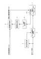
図1に実施の形態の表示装置の構成を示す。本例の表示装置は、有機EL素子を発光素子として用いる有機ELディスプレイパネルモジュール1と、ダミー画素情報加算部2と、表示信号検出部3と、駆動電圧決定部4と、駆動電圧可変部5と、アノード電位検出部6を備える。Embodiments of a display device and a display driving method according to the present invention will be described below.
FIG. 1 shows a configuration of a display device according to an embodiment. The display device of this example includes an organic EL
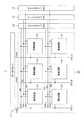
まず図2、図3、図4、図5、図6を参照して有機ELディスプレイパネルモジュール1について述べる。
図2に有機ELディスプレイパネルモジュール1の構成の一例を示す。この有機ELディスプレイパネルモジュール1は、有機EL素子を発光素子とし、アクティブマトリクス方式で発光駆動を行う画素回路10を含むものである。
図2に示すように、有機ELディスプレイパネルモジュール1は、画素回路10が列方向と行方向にマトリクス状に配列された画素アレイ部20と、データドライバ11と、ゲートドライバ12,13,14を備える。
またデータドライバ11により選択され、供給される表示データ信号に応じた信号値Vsigを画素回路10に対する入力信号として供給する信号線DTL1、DTL2・・・が、画素アレイ部20に対して列方向に配されている。信号線DTL1、DTL2・・・は、画素アレイ部20においてマトリクス配置された画素回路10の列数分だけ配される。First, the organic EL
FIG. 2 shows an example of the configuration of the organic EL
As shown in FIG. 2, the organic EL
Further, signal lines DTL1, DTL2,..., Which are selected by the
また画素アレイ部20に対して、行方向に走査線WSL1,WSL2・・・、走査線DSL1,DSL2・・・、走査線RSL1,RSL2・・・が配されている。これらの走査線WSL、DSL,RSLは、それぞれ、画素アレイ部20においてマトリクス配置された画素回路10の行数分だけ配される。
走査線WSL(WSL1,WSL2・・・)は、画素回路10への信号値Vsigの書込(ライトスキャン)を行うための走査線であり、ゲートドライバ12により駆動される。ゲートドライバ12は、設定された所定のタイミングで、行状に配設された各走査線WSL1,WSL2・・・に順次、走査パルスWSを供給して、画素回路10を行単位で線順次走査する。
走査線DSL(DSL1,DSL2・・・)はゲートドライバ13により駆動される。ゲートドライバ13は、有機EL素子の発光駆動のための走査パルスDSを、行状に配設された各電源線DSL1,DSL2・・・にそれぞれ所定タイミングで供給する。
走査線RSL(RSL1,RSL2・・・)はゲートドライバ14により駆動される。ゲートドライバ14は、画素回路10のリセット動作のための走査パルスRSを、行状に配設された各走査線RSL1,RSL2・・・にそれぞれ所定タイミングで供給する。
データドライバ11は、ゲートドライバ12による線順次走査に合わせて、列方向に配された信号線DTL1、DTL2・・・に対して、画素回路10に対する入力信号としての信号値(Vsig)を供給する。Further, scanning lines WSL1, WSL2,..., Scanning lines DSL1, DSL2,..., Scanning lines RSL1, RSL2,. These scanning lines WSL, DSL, and RSL are respectively arranged by the number of rows of the
The scanning lines WSL (WSL1, WSL2,...) Are scanning lines for writing the signal value Vsig to the pixel circuit 10 (write scanning), and are driven by the
The scanning lines DSL (DSL1, DSL2,...) Are driven by the
The scanning lines RSL (RSL1, RSL2,...) Are driven by the
The
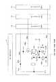
図3に画素回路10の構成を示している。この画素回路10が、図2の構成における画素回路10のようにマトリクス配置される。なお、図3では簡略化のため、信号線DTLと走査線WSL、DSL、RSLが交差する部分に配される1つの画素回路10のみを示している。
実施の形態として採用できる画素回路10の構成は多様に考えられるが、この例では、画素回路10は、発光素子である有機EL素子30と、1個の保持容量Csと、サンプリングトランジスタTr1、駆動トランジスタTr2、スイッチングトランジスタTr3、リセット用トランジスタTr4としての4個の薄膜トランジスタ(TFT)とで構成されている。各トランジスタTr1、Tr2、Tr3、Tr4はnチャネルTFTとされている。FIG. 3 shows the configuration of the
Various configurations of the
保持容量Csは、一方の端子が駆動トランジスタTr2のソースに接続され、他方の端子が同じく駆動トランジスタTr2のゲートに接続されている。
画素回路10の発光素子は例えばダイオード構造の有機EL素子30とされ、アノードとカソードを備えている。有機EL素子1のアノードは駆動トランジスタTr2のソースに接続され、カソードは所定の接地配線(カソード電位Vcath)に接続されている。
サンプリングトランジスタTr1は、そのドレインとソースの一端が信号線DTLに接続され、他端が駆動トランジスタTr2のゲートに接続される。またサンプリングトランジスタのゲートは走査線WSLに接続されている。
スイッチングトランジスタTr3は、そのドレインとソースの一端が電源電圧Vccに接続され、他端が駆動トランジスタTr2のドレインに接続される。またスイッチングトランジスタTr3のゲートは走査線DSLに接続されている。
リセット用トランジスタTr4は、そのドレインとソースの一端が駆動トランジスタTr2のソースに接続され、他端が所定のリセット電位Vrsに接続される。またリセット用トランジスタTr4のゲートは走査線RSLに接続されている。The holding capacitor Cs has one terminal connected to the source of the drive transistor Tr2, and the other terminal connected to the gate of the drive transistor Tr2.
The light emitting element of the
The sampling transistor Tr1 has one end of its drain and source connected to the signal line DTL, and the other end connected to the gate of the driving transistor Tr2. The gate of the sampling transistor is connected to the scanning line WSL.
The switching transistor Tr3 has one end of its drain and source connected to the power supply voltage Vcc, and the other end connected to the drain of the driving transistor Tr2. The gate of the switching transistor Tr3 is connected to the scanning line DSL.
The reset transistor Tr4 has one end of its drain and source connected to the source of the drive transistor Tr2, and the other end connected to a predetermined reset potential Vrs. The gate of the reset transistor Tr4 is connected to the scanning line RSL.
このような画素回路10の動作を図4を参照して簡単に説明する。図4(a)は信号線DTLに与えられる信号値Vsig、図4(b)は水平同期信号HS、図4(c)は走査線WSLからサンプリングトランジスタTr1のゲートに与えられる走査パルスWS、図4(d)は走査線RSLからリセット用トランジスタTr4のゲートに与えられる走査パルスRS、図4(e)は駆動トランジスタTr2のゲート電圧Vg、図4(f)は駆動トランジスタTr2のソース電圧Vs、図4(g)は走査線DSLからスイッチングトランジスタTr3のゲートに与えられる走査パルスDSを、それぞれ示している。 The operation of the
水平同期信号HSによって水平走査の開始時点が決められる。そして図における書込期間として、信号線DTLに信号値Vsigが印加される。この書込期間には、走査パルスWSによってサンプリングトランジスタTr1が導通されることで、信号線DTLからの信号値Vsigが保持容量Csに書き込まれる。
また、この書込期間には、走査パルスRSによりリセット用トランジスタTr4が導通され、保持容量Csの他端側がリセット電位Vrsとされる。これは保持容量Csの他端側の電位が不定であると、保持容量Csに書き込まれる電圧が、信号値Vsigと同じにならないためである。
結果として、この書込期間では、駆動トランジスタTr2のゲート電圧は、保持容量Csへの信号値Vsigの書込に応じて上昇する。一方、駆動トランジスタTr2のソース電圧Vsは、リセット電位Vrsに維持される。The start point of horizontal scanning is determined by the horizontal synchronization signal HS. As a writing period in the figure, the signal value Vsig is applied to the signal line DTL. In this writing period, the sampling transistor Tr1 is turned on by the scanning pulse WS, so that the signal value Vsig from the signal line DTL is written to the holding capacitor Cs.
In this writing period, the reset transistor Tr4 is turned on by the scanning pulse RS, and the other end side of the storage capacitor Cs is set to the reset potential Vrs. This is because if the potential on the other end side of the storage capacitor Cs is indefinite, the voltage written to the storage capacitor Cs does not become the same as the signal value Vsig.
As a result, in this writing period, the gate voltage of the drive transistor Tr2 rises according to the writing of the signal value Vsig to the storage capacitor Cs. On the other hand, the source voltage Vs of the drive transistor Tr2 is maintained at the reset potential Vrs.
書込期間に続いて発光期間としての動作が行われる。発光期間では、走査パルスWS、RSがLレベルとされてサンプリングトランジスタTr1、リセット用トランジスタTr4がオフとされ、一方、走査パルスDSによってスイッチングトランジスタTr3が導通される。これによって駆動電源電圧Vccからの電流供給により、駆動トランジスタTr2が保持容量Csに保持された信号電位(即ち駆動トランジスタTr2のゲート・ソース間電圧)に応じた電流を有機EL素子30に流し、有機EL素子30を発光させる。駆動トランジスタTr2は飽和領域で動作し、有機EL素子30に対して、信号値Vsigに応じた駆動電流を与える定電流源として機能する。
以上のような動作により画素回路10の発光駆動が行われる。
なお、有機EL素子30に電流が流れることで有機EL素子30の両端電圧が上昇するため、発光期間当初は、これに伴って駆動トランジスタTr2のゲート電圧Vgとソース電圧Vsが上昇する。Following the writing period, an operation as a light emission period is performed. In the light emission period, the scanning pulses WS and RS are set to the L level, the sampling transistor Tr1 and the reset transistor Tr4 are turned off, and the switching transistor Tr3 is turned on by the scanning pulse DS. As a result, by supplying a current from the drive power supply voltage Vcc, a current corresponding to the signal potential (that is, the voltage between the gate and source of the drive transistor Tr2) held in the holding capacitor Cs by the drive transistor Tr2 is caused to flow through the
The light emission driving of the
In addition, since the both-ends voltage of the
有機ELディスプレイパネルモジュール1は、基本的には以上のような構成及び動作となるが、本例の場合、有機ELディスプレイパネルモジュール1は、配列されている画素回路10の一部がダミー画素回路10dとされている。
図5は、ダミー画素回路10dを、上記図3と同様の形式で示している。この図5からわかるように、ダミー回路10dは、画素回路構成は、他の通常の画素回路10と同様である。但し、有機EL素子30のアノード電圧を検出するための検出端子31が用意されている。
なお、本例では、有機EL素子30のカソード電圧Vcathは固定電位であるとしており、このため、検出端子31でアノード電圧を検出すれば、アノード−カソード間電圧を検出できることになる。The organic EL
FIG. 5 shows the
In this example, the cathode voltage Vcath of the
このようなダミー画素回路10dとしては、画素の表示色毎に設けられる。即ち通常の画素回路としては、R(赤)、G(緑)、B(青)の各画素回路が形成されているが、ダミー画素回路10dとしても、Rダミー画素回路10dR、Gダミー画素回路10dG、Bダミー画素回路10dBが設けられている。 Such a
図6(a)(b)はダミー画素回路10dの配置エリアについて示したものである。図6(a)(b)においては図2に示した画素アレイ部20を模式的に示している。即ち多数の画素回路10が配列されている領域である。
この画素アレイ部20において、表示エリア21が、実際に画像表示を行う表示領域(ユーザによって画像が視認される領域)であるとすると、図6(a)のように斜線部で示す、表示エリア21の周囲において、ダミー画素回路10dを設けることが考えられる。
また、後述するが、本例の動作のポイントの一つとしては、発光駆動用電源電圧を過低減させてしまうことによる発光輝度の低下が引き起こす画質の低下を必ず防止することである。有機EL素子30の両端電圧(アノード−カソード間電圧)は、低温であるほど高いという特性があるため、ダミー画素回路10dは、なるべく表示領域内で発光して発熱する温度の影響を受けない位置に配置されることが望ましい。
そして表示装置は通常主に立てて使用することがほとんどであることを考慮すると、発光による熱が空気の対流の影響を受けないように画面の上側への配置を避け、図6(b)の斜線部のように画面の下側に配置を行うようにすると好適である。6A and 6B show the arrangement area of the
In the
As will be described later, one of the points of the operation of this example is to prevent the deterioration of the image quality caused by the decrease of the light emission luminance due to the excessive reduction of the light emission driving power supply voltage. Since both ends voltage (anode-cathode voltage) of the
In view of the fact that the display device is usually used mainly in an upright position, avoid disposing the display device on the upper side of the screen so that the heat generated by light emission is not affected by air convection. It is preferable that the arrangement is performed on the lower side of the screen as indicated by the hatched portion.
図1に戻って、本例の構成を説明する。
表示データ信号は、表示信号検出部3及びダミー画素情報加算部2に供給される。
表示信号検出部3は、有機ELディスプレイパネルモジュール1に対して供給されるべき表示データ信号について、例えば1フレーム期間ごとに、表示色毎の最大階調値を抽出する。
ここでいう最大階調値とは、或る1フレームにおいて各画素に与える輝度値のうちで、最も高輝度となる値のことであり、つまり1フレーム内での、最も高輝度で発光させる画素に対する表示データ信号値のことである。
このような最大階調値を、R、G、B各色毎に検出する。
従って、1フレーム期間の表示データ信号のうちのR画素回路に対応する信号値(輝度値)について、順次比較処理を行っていくことで、1フレーム期間内でのR画素についての最大階調値を検出する。同様に、B画素、G画素についても、それぞれ最大階調値を検出する。
なお、表示信号検出部2にフレームメモリを用意し、1フレーム期間の表示データ信号値を一時的に記憶して、その中からR、G、B各色毎の最大階調値を検出するようにしてもよい。
表示信号検出部3は、このようにして検出した、R、G、B各色についての1フレーム期間の最大階調値を、ダミー画素情報加算部2に供給する。Returning to FIG. 1, the configuration of this example will be described.
The display data signal is supplied to the display signal detection unit 3 and the dummy pixel
For the display data signal to be supplied to the organic EL
The maximum gradation value here is a value that gives the highest brightness among the brightness values given to each pixel in a certain frame, that is, a pixel that emits light with the highest brightness in one frame. Is the display data signal value for.
Such a maximum gradation value is detected for each color of R, G, and B.
Therefore, by sequentially comparing the signal values (luminance values) corresponding to the R pixel circuit in the display data signal in one frame period, the maximum gradation value for the R pixel in one frame period. Is detected. Similarly, the maximum gradation value is detected for each of the B pixel and the G pixel.
Note that a frame memory is prepared in the display
The display signal detector 3 supplies the dummy
ダミー画素情報加算部2は、表示データ信号に、表示信号検出部3から入力される色別の1フレームごとの最大階調値を、ダミー画素回路10dR,10dG,10dB用のデータ信号として加算処理し、上述のようにダミー画素回路10d(10dR,10dG,10dB)を有した有機ELディスプレイパネルモジュール1に出力する。
なおこの際、フレームメモリなどを用い、ダミー画素回路10d用の表示内容に対し、実際の表示データ信号(通常の表示用の画素回路10に対する表示データ信号)のみを1フレーム遅延させるようにし、表示エリア21の表示内容に対し、適正な発光駆動用電源電圧Vccの供給が行えるよう、出力遅延コントロールを行う。
つまり、ダミー画素回路10dに与える表示データ信号は、次のフレーム期間に表示エリア21において表示される表示内容での最大階調値となるようにする。
これは、後述するようにダミー画素回路10dにおいて有機EL素子30のアノード−カソード間電圧を検出して、その検出結果に応じて電源電圧Vccを制御した後のタイミング(即ち1フレーム後)で、ダミー画素回路10dに与えた最大階調値を含む画像内容が表示エリア21に表示されるようにするためである。The dummy pixel
At this time, a frame memory or the like is used so that only the actual display data signal (display data signal for the normal display pixel circuit 10) is delayed by one frame with respect to the display content for the
That is, the display data signal given to the
As described later, this is the timing after detecting the anode-cathode voltage of the
ダミー画素情報加算部2から有機ELディスプレイパネルモジュール1に表示データ信号が供給されることで、有機ELディスプレイパネルモジュール1では、上述のように表示データ信号に基づいて、各画素回路10及びダミー画素回路10dに信号値Vsigが与えられ、画像表示が実行される。 When the display data signal is supplied from the dummy pixel
有機ELディスプレイパネルモジュール1においては、発光が行われたダミー画素回路10dの有機EL素子30のアノード電圧が、アノード電位検出部6で検出される。
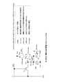
図7に有機ELディスプレイパネルモジュール1における色毎のダミー画素回路10dR、10dG、10dBと、アノード電位検出部6の構成例を示している。
アノード電位検出部6は、Rダミー画素回路10dRの検出端子31から得られるアノード電圧を、アンプ61Rを介してA/D変換器62Rに入力し、R画素についてのデジタル値としてのアノード電圧値Va_rを得る。
またGダミー画素回路10dGの検出端子31から得られるアノード電圧を、アンプ61Gを介してA/D変換器62Gに入力し、G画素についてのデジタル値としてのアノード電圧値Va_gを得る。
さらにBダミー画素回路10dBの検出端子31から得られるアノード電圧を、アンプ61Bを介してA/D変換器62Bに入力し、B画素についてのデジタル値としてのアノード電圧値Va_bを得る。
これらR、G、B各色についてのアノード電圧値Va_r、Va_g、Va_bを比較演算部63に入力する。比較演算部63は、色別のアノード電圧値(Va_r、Va_g、Va_b)の中から最大値(Vamax)の抽出を行い、その情報を駆動電圧決定部4に出力する。In the organic EL
FIG. 7 shows a configuration example of the
The anode potential detector 6 inputs the anode voltage obtained from the
The anode voltage obtained from the
Further, the anode voltage obtained from the
The anode voltage values Va_r, Va_g, and Va_b for these R, G, and B colors are input to the
駆動電圧決定部4は、アノード電圧の最大値Vamaxから、最適Vcc値を算出し、その情報を駆動電圧可変部5に出力する。なお、最適Vcc値の算出手法例については後述する。
駆動電圧可変部5は、所定の電圧値として設定されている駆動電源電圧(Vcc)について、電圧値を変換して有機ELディスプレイパネルモジュール1に供給する。この駆動電圧可変部5から出力される駆動電源電圧Vccは、有機ELディスプレイパネルモジュール1の全ての画素回路10(及び10d)に共通に供給される。
この駆動電圧可変部5は、入力されるEL駆動電源電圧について、駆動電圧決定部4で決定される最適Vcc値に変換し(最適EL駆動電源電圧)、有機ELディスプレイパネルモジュール1に供給する。電圧変換手法の例については後述する。The drive
The drive voltage
The drive voltage
このような本例の表示装置についての動作を説明していく。
まず、図8により、一般的な発光駆動用電源電圧Vccの決定手法について述べる。ここで決定される一般的な電源電圧Vccとは、本例では図1の駆動電圧可変部5に入力される段階(電圧値変換前)の電源電圧値となる。The operation of the display device of this example will be described.
First, a general method for determining the power supply voltage Vcc for light emission driving will be described with reference to FIG. In this example, the general power supply voltage Vcc determined here is a power supply voltage value at a stage (before voltage value conversion) input to the drive
図8では上述した画素回路10を示しているが、駆動トランジスタTr2が、そのゲート・ソース間電圧Vgsに対応した一定電流を流し続ける(飽和領域動作を保証する)ためには、ドレイン・ソース間電圧Vds間がある電位以上に保たれなくてはならない。その為の電位を図示するVds(sat)とすると、電源電圧Vcc−カソード電位Vcath間の電圧は、いかなる駆動環境/条件であろうとも、このドレイン・ソース間電圧Vds(sat)を割り込まないように決められることが一般的である。
電源電圧Vcc−カソード電位Vcath間には、画素回路の構成上、最低使用環境温度/仕様最高輝度(仕様最大電流)における有機EL素子30の最大両端(アノード−カソード間)電圧:VEL(MAX)と、上記のドレイン・ソース間電圧Vds(sat)、さらにスイッチングトランジスタTr3のオン時に発生するワースト最大電圧:VDS(on)の3つに、I−V特性劣化マージン分:Vmarginを加えた要素が存在する。このため、これらの加算で電源電圧Vccが決定される。
なおI−V特性劣化マージン分とは、有機EL素子30の経時劣化を考慮したマージンである。Although FIG. 8 shows the
Between the power supply voltage Vcc and the cathode potential Vcath, the maximum voltage (between the anode and cathode) of the
The IV characteristic deterioration margin is a margin considering deterioration with time of the
決定される電源電圧Vcc値をVcc_defaultとすると、
Vcc_default=Vcath+VEL(MAX)+Vds(sat)+VDS(on)+Vmargin
として算出される。
仕様から決まる輝度、即ち電流値Idsは、有機ELデバイスによって決まってしまい、駆動電圧に左右されないため、Vcc_default×Idsで算出される消費電力の低減化は、Vcc_defaultを如何に下げられるかにかかっている。If the determined power supply voltage Vcc value is Vcc_default,
Vcc_default = Vcath + VEL (MAX) + Vds (sat) + VDS (on) + Vmargin
Is calculated as
The luminance determined by the specification, that is, the current value Ids is determined by the organic EL device and does not depend on the drive voltage. Yes.
従来は、このようにマージンを持った最大の定電圧(Vcc_default)を、発光駆動電源電圧Vccとして与え続けており、通常平均的に使用される階調や環境温度を考えても無駄に電力を消費している状態が意外に多い。
本例では、有機EL素子30の両端電圧VEL(アノード−カソード間電圧)を、ダミー画素回路10dから検出するが、これは、環境温度と階調による両端電圧変動、及びI−V特性劣化による両端電圧変動を含んだうえでの、両端電圧VEL値である。
この検出された両端電圧VELに応じて電源電圧Vccを可変することで、無駄な電力消費分を削減する。Conventionally, the maximum constant voltage (Vcc_default) having a margin as described above has been continuously applied as the light emission drive power supply voltage Vcc, and power is wasted even in consideration of the gradation and environmental temperature that are normally used on average. There are unexpectedly many consumption states.
In this example, the both-end voltage VEL (anode-cathode voltage) of the
By varying the power supply voltage Vcc according to the detected both-end voltage VEL, useless power consumption is reduced.
特に言えば、有機EL素子30の最大両端電圧VEL(MAX)は、あくまでも最低使用環境温度/仕様最高輝度(仕様最大電流)を想定しているものであるが、常に最低の使用環境温度の条件下で、常に最大の輝度の発光状態であるものではないにもかかわらず、このような最大両端電圧VEL(MAX)を考慮して電源電圧Vccを決めなければならないため、無駄な電力消費が生じていた。
そこで本例では、環境温度、階調、特性劣化に応じて変動する有機EL素子30の両端電圧VELの変動に応じて、電源電圧Vccを可変する。つまりは、上記のVcc_default算出式におけるVEL(MAX)が低下する分だけ、電源電圧Vccを低下させるという考え方で、無駄な電力消費分を削減するものである。In particular, the maximum voltage VEL (MAX) across the
Therefore, in this example, the power supply voltage Vcc is varied according to the variation of the voltage VEL across the
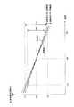
図9は有機EL素子30のI−V特性の温度特性一例である。ここでは高温(60℃)、常温(25℃)、低温(−10℃)のそれぞれにおいて、有機EL素子に流れる電流Idsと有機EL素子30の両端電圧VELの特性を示している。
図からわかるように有機EL素子30のI−V特性は、温度が高くなるに連れて低電圧側へ、温度が低くなるに連れて高電圧側へと、電流に対する電圧の特性が変動する。
併せて、電流値によって、温度によるシフト(変動)している量が変わってもいる。例えば電流値aの状態では、低温時と高温時の間の両端電圧VELの変動はΔVaとなるが、電流値bの状態では、低温時と高温時の間の両端電圧VELの変動はΔVbとなる(ΔVa>ΔVb)。
また、温度に応じた両端電圧VELの変動比率は、R、G、Bの各色毎でも異なる。FIG. 9 is an example of the temperature characteristic of the IV characteristic of the
As can be seen from the figure, the IV characteristic of the
In addition, the amount of shift (fluctuation) due to temperature varies depending on the current value. For example, in the state of the current value a, the fluctuation of the both-end voltage VEL between the low temperature and the high temperature becomes ΔVa, but in the state of the current value b, the fluctuation of the both-end voltage VEL between the low temperature and the high temperature becomes ΔVb (ΔVa> ΔVb).
Further, the variation ratio of the both-end voltage VEL according to the temperature is different for each color of R, G, and B.
図10は、図9のグラフから抽出される、温度による有機EL素子30の両端電圧VEL(アノード−カソード間電圧(カソード電位固定の場合はアノード電圧))の変化を表したもので、発光輝度(電流)によりその変化量に差があることを示す一例である。ここでは実線は中間的な輝度、破線は高輝度、一点鎖線は低輝度の各場合において温度状況に応じた有機EL素子30の両端電圧VELの変化を示している。例えば高輝度発光の場合において−10℃と60℃の場合の両端電圧VELの変動量を1とした場合、低輝度発光時における−10℃と60℃の場合の両端電圧VELの変動量は0.95となる。 FIG. 10 shows a change in the voltage VEL (anode-cathode voltage (anode voltage when the cathode potential is fixed)) of the
図11は、有機EL素子30のI−V特性劣化の一例を示したものである。
有機EL素子30は、発光量に応じてI−V特性が劣化していく性質を持っており、時間と共に、同電流に対する電圧が上昇していく傾向を示している。図では、実線、一点鎖線、破線の順序で、経時的な特性の変動を示している。
なお従って、同じ輝度を維持するためには、時間がたつにつれ、初期から比較して、より高い発光駆動用電源電圧が必要になってくることを示している。通常、上述したように、使用推定寿命から、劣化変動するI−V特性分をマージン分(Vmargin)として含まれた、初期発光駆動用電源電圧(Vcc_default)が設定されるものである。FIG. 11 shows an example of the IV characteristic deterioration of the
The
Therefore, in order to maintain the same luminance, it is shown that a higher power supply voltage for light emission driving is required from the initial stage as time passes. Normally, as described above, the initial light emission drive power supply voltage (Vcc_default) is set, which includes the IV characteristics that change in deterioration as a margin (Vmargin) from the estimated service life.
このように有機EL素子30の両端電圧VELは、温度と発光輝度(電流値)に応じて変動し、また経時的な変動も生じる。
本例では、これら環境温度と電流値(発光階調)、さらには経時劣化成分を含んだ有機EL素子30の両端電圧VELの変動に応じて、電源電圧Vccを可変することで、発光輝度に影響を与えずに、効果的に消費電力を低減させる。As described above, the voltage VEL across the
In this example, by changing the power supply voltage Vcc according to the environmental temperature and current value (light emission gradation), and also the fluctuation of the voltage VEL across the
上述のように発光駆動用の電源電圧Vccは、図1に示した駆動電圧可変部5で可変して有機ELディスプレイパネルモジュール1に供給するが、この電源電圧可変のための動作を説明していく。
図12は、電源電圧Vccを可変させるための各部の処理を示したものである。以下の<S1>〜<S4>としての各処理が行われ、駆動電圧可変部5に最適Vcc値の情報が供給される。As described above, the power supply voltage Vcc for driving light emission is varied by the drive
FIG. 12 shows processing of each part for varying the power supply voltage Vcc. The following processes as <S1> to <S4> are performed, and information on the optimum Vcc value is supplied to the drive voltage
まず処理<S1>として、アノード電位検出部6は、色別のダミー画素回路10dR、10dG、10dBを、1フレーム内での最大階調値で発光させたときのアノード電圧Va_r、Va_g、Va_bを検出し、デジタル値に変換する。
なお、上述したように、ダミー画素情報加算部2では、実際の表示データ信号(通常の表示用の画素回路10に対する表示データ信号)を、ダミー画素回路10d用の表示データ信号に対して1フレーム遅延させるようにして有機ELディスプレイパネルモジュール1に供給するため、この処理<S1>の際にダミー画素回路10dR、10dG、10dBに与えている信号値は、次のフレームの表示データ信号内での最大階調値となる。First, as the process <S1>, the anode potential detection unit 6 uses the anode voltages Va_r, Va_g, and Va_b when the dummy pixels 10dR, 10dG, and 10dB for each color emit light at the maximum gradation value within one frame. Detect and convert to digital value.
As described above, in the dummy pixel
次に処理<S2>として、アノード電位検出部6は、色別のアノード電圧(Va_r、Va_g、Va_b)の中から最大のものを選択し、最大値Vamaxとして抽出する。この最大値Vamaxは、駆動電圧決定部4に送られる。
なお、色別のアノード電圧(Va_r、Va_g、Va_b)の中から最大のものを選択して、最大値Vamaxを、有機EL素子30のアノード−カソード間電圧の情報として駆動電圧決定部4に送るのは、有機EL素子30のアノード−カソード間電圧の温度による変動率が、色毎にも異なるためである。即ち、ここでは色毎の変動率も考慮して、あくまでも、現フレームとしての最大のアノード−カソード間電圧を検出するためである。Next, as a process <S2>, the anode potential detection unit 6 selects the maximum one of the anode voltages (Va_r, Va_g, Va_b) for each color and extracts it as the maximum value Vamax. This maximum value Vamax is sent to the drive
Note that the maximum one of the anode voltages (Va_r, Va_g, Va_b) for each color is selected, and the maximum value Vamax is sent to the drive
処理<S3>では、駆動電圧決定部4が、供給された最大値Vamaxを用い、有機EL素子30の両端電圧VELの仕様上ワーストとして設定した、VEL(max)+Vmarginに対し、現在のワーストVELがどの程度下がっているかの変化量ΔVELを次式にて算出する。
ΔVEL=VEL(max)+Vmargin−Vamax
これにより、所定輝度に対し、輝度の低下を引き起こさせずに下げられる最大の電圧ΔVELを正確に把握できる。In the process <S3>, the drive
ΔVEL = VEL (max) + Vmargin−Vamax
Thereby, it is possible to accurately grasp the maximum voltage ΔVEL that can be lowered without causing a decrease in luminance with respect to the predetermined luminance.
そして処理<S4>で駆動電圧決定部4は、最適Vcc値を次式で算出する。
最適Vcc値=Vcc_default−ΔVEL
即ち初期電源電圧値Vcc_defaultから変化量ΔVELを減じた結果が、画質を低下させずに消費電力を最大に削減することのできる、最適Vcc値となる。
この最適Vcc値の情報は、駆動電圧可変部5に送られ、発光駆動用電源電圧Vccの低減変換が行われる。Then, in the process <S4>, the drive
Optimum Vcc value = Vcc_default−ΔVEL
That is, the result of subtracting the change amount ΔVEL from the initial power supply voltage value Vcc_default is the optimum Vcc value that can reduce the power consumption to the maximum without degrading the image quality.
The information on the optimum Vcc value is sent to the drive voltage
図13は、駆動電圧可変部5の構成の一例を示している。例えば図のように電源可変コントロール部51,デジタルポテンショメータ52、抵抗R1を備えた構成とされる。
電源可変コントロール部51は、入力電圧Vinについて電圧可変した出力電圧Voutを得る。
一般的な、電源可変コントロール回路は、スイッチングレギュレータとシリーズレギュレータに大別されるが、出力電圧Voutを可変コントロールする手法は基本的に同一である。電圧可変量を比較的多く取りたい場合は、効率の関係上スイッチングレギュレータが選択されることがほとんどである。
電源可変コントロール部51には、出力電圧をある電位でフィードバックさせるためのFB端子が設けられており、この電位をある一定値に保とうとする動作で出力電圧を安定化させる。FB電位は一般的に1〜3V程度であるため、出力電圧を抵抗分圧し、FB端子に接続する構成により、電圧可変制御が可能となる。
即ちFB電位はある値(例えば2V)で決められているため、出力電圧を可変させるためには抵抗分圧の比を変えてやれば良い。
このために一方を固定抵抗R1、もう一方を抵抗値可変のディジタル制御が可能なディジタルポテンショメータ52を使用する。駆動電圧決定部4が、最適Vcc値を得るためのデジタル値をデジタルポテンショメータ52に供給し、抵抗値を可変制御することで、出力電圧Vout、即ち発光駆動用電源電圧Vccをコントロールできる。FIG. 13 shows an example of the configuration of the drive voltage
The power supply
General power supply variable control circuits are roughly classified into a switching regulator and a series regulator, but the method of variably controlling the output voltage Vout is basically the same. When it is desired to take a relatively large amount of variable voltage, a switching regulator is often selected for efficiency.
The power supply
That is, since the FB potential is determined by a certain value (for example, 2 V), the resistance voltage dividing ratio may be changed in order to vary the output voltage.
For this purpose, a
以上の動作により本例の表示装置では、色毎のダミー画素回路10dR、10dG、10dBから検出したアノード電圧値(有機EL素子30の両端電圧VEL)に応じて、発光駆動用電源電圧Vccが可変制御される。
そして、このように可変制御された発光駆動用電源電圧Vccは、次のフレーム期間に各画素回路10に供給される。このとき、発光駆動用電源電圧Vccは、そのフレームの表示データ信号における最大階調値の電流を有機EL素子30に流した場合でのアノード電圧値に基づいて、電圧値がコントロールされたものとなる。With the above operation, in the display device of this example, the light emission drive power supply voltage Vcc is variable according to the anode voltage value (the voltage VEL across the organic EL element 30) detected from the dummy pixel circuits 10dR, 10dG, and 10dB for each color. Be controlled.
The light emission driving power supply voltage Vcc variably controlled in this way is supplied to each
このように本実施の形態では、有機ELディスプレイパネルモジュール1の表示エリア31外にアノード電圧(アノード−カソード間電圧:両端電圧VEL)を検出できるダミー画素回路10dを色別に設け、そのダミー画素回路を常に1フレーム内の最大階調値で発光させることによって、表示エリア31内に存在する最大階調で発光する画素の有機EL素子30の両端電圧VELを、ダミー画素回路10dを利用して検出するようにしている。このダミー画素回路10dから検出されるアノード電圧は、その時の有機EL素子30の温度状態を的確に反映したものであり、環境温度などを検出せずに、正確にターゲットとする有機EL素子30の両端電圧VELを把握できるようになる。また、IV特性の劣化についてもある程度体現するため、初期において劣化マージン分のさらなる消費電力低減も可能になる。このようなアノード電圧の検出情報を元に、発光駆動用電源電圧Vccの低減コントロールを行うことで、不必要な電力消費分を、より正確かつ確実に、削減することができるようになる。
そして、自発光型フラットパネルディスプレイの画質低下を視認させないように低消費電力化を図ることが実現できるため、表示装置をバッテリ動作機器とすれば、動作時間を長時間化することに貢献し、またACコンセントから電源を得る機器であれば節電や電気代の節約に貢献できることになる。As described above, in this embodiment,
And since it is possible to achieve low power consumption so as not to visually recognize the degradation of the image quality of the self-luminous flat panel display, if the display device is a battery-operated device, it contributes to longer operating time, In addition, a device that obtains power from an AC outlet can contribute to saving power and saving electricity costs.
両端電圧VELとしては5V以上変化する有機EL素子も存在するため、以上のように両端電圧VELの変動特性に応じて電源電圧Vccを低下させることで、消費電力の低減を効果的に実現できる。
消費電力はVcc×Idsで算出されるため、電源電圧Vccが電圧低下後の発光駆動用電源電圧値だとすると、Vcc_defaultに対する電圧値の低減比がそのまま、消費電力の低減比になる。仮にVcc_defaultを15V、Vccを10Vとし、5Vの電圧低減コントロールを行ったとすると、消費電力の最大低減比率は約67%にもなるという大きな効果を得られることになる。Since there is an organic EL element that changes by 5 V or more as the both-end voltage VEL, the power consumption can be effectively reduced by reducing the power supply voltage Vcc according to the fluctuation characteristics of the both-end voltage VEL as described above.
Since the power consumption is calculated as Vcc × Ids, assuming that the power supply voltage Vcc is the power supply voltage value for light emission driving after the voltage drop, the reduction ratio of the voltage value with respect to Vcc_default is the same as the reduction ratio of power consumption. If Vcc_default is 15 V, Vcc is 10 V, and voltage reduction control of 5 V is performed, the maximum reduction ratio of power consumption can be as large as about 67%.
発光輝度に影響を与えない範囲で電源電圧Vccを可変できるのは、映像信号(表示データ信号)から1フレームごとに最大階調値を検出していることによる。つまり、フレーム毎に、有機EL素子30に流す電流量の最大値を基準として、その際の両端電圧VELに応じて、最低限必要な電源電圧Vccが画素回路10に供給されるようにしているためである。
これによって発光駆動用電源電圧Vccが、下げすぎになることを確実に防止でき、適正な輝度での発光状態を確保した上で、最大限の消費電力削減の効果を実現できる。The reason why the power supply voltage Vcc can be varied within a range that does not affect the light emission luminance is that the maximum gradation value is detected for each frame from the video signal (display data signal). That is, for each frame, the minimum required power supply voltage Vcc is supplied to the
As a result, it is possible to reliably prevent the light emission driving power supply voltage Vcc from being lowered excessively, and it is possible to achieve the maximum power consumption reduction effect while ensuring a light emission state with appropriate luminance.
また、経時劣化による有機EL素子30のI−V特性の変動については、発光量の推定を積算していく手法もあるが、膨大な時間に亘って累積計算をしなければならないことでの規模増と、あくまで推定計算であることからの誤差の大きさが考えられ、精度をある程度制限することを強いられるが、本例のようにアノード電圧の検出によって、経時劣化による変動成分も含んで制御できるため、このような点は全く解消される。 In addition, regarding the variation of the IV characteristics of the
また発光駆動用電源電圧Vccは、駆動電圧可変部5で得られるが、この駆動電圧可変部5をシリーズレギュレータや降圧型スイッチングレギュレータによって構成すれば、電源電圧値を下げた場合に、有機ELディスプレイパネルモジュール1で消費している電力をレギュレータ側に移すことで、有機ELディスプレイパネルモジュール1自体で消費している電力を下げ、有機ELデバイスの温度を低く抑えることとなる。
または、駆動電圧可変部5を、ある出力電圧範囲の間において、変換効率の変化しない/変化が少ない昇圧型スイッチングレギュレータによって構成すれば、電源電圧値を下げた場合に、有機ELディスプレイパネルモジュール1自体で消費している電力を下げ、有機ELデバイスの温度を低く抑えるようにすることに加え、機器全体の消費電力をも下げられるようになる。The light emission drive power supply voltage Vcc is obtained by the drive voltage
Alternatively, if the drive voltage
実施の形態としては、多様な変形例が考えられる。
例えば上記例では、全ての画素回路に共通の電源電圧Vccを与える構成を示したが、画素回路10としては、R(赤)用画素回路、G(緑)用画素回路、B(青)用画素回路が配列されている。これら色毎の画素回路に対してそれぞれ電源電圧Vccラインを独立して設け、上記電源電圧Vccの可変処理を色毎に行うようにしてもよい。
その場合、各色についてのダミー画素回路10dで得られるアノード電圧に基づいて、その色の電源電圧の可変制御を行うようにすればよい。
また、ダミー画素回路10dを色別には設けない例も考えられる。Various modifications can be considered as the embodiment.
For example, in the above example, the configuration in which the common power supply voltage Vcc is applied to all the pixel circuits is shown. However, as the
In that case, based on the anode voltage obtained by the
An example in which the
また、上記例では、表示信号検出部3では1フレーム単位で色別の最大階調値を検出したが、2フレーム単位など、他の所定期間で、色別の最大階調値を検出し、それを当該所定期間でのダミー画素回路10dに与える信号値としてもよい。 In the above example, the display signal detection unit 3 detects the maximum gradation value for each color in units of one frame, but detects the maximum gradation value for each color in another predetermined period, such as in units of two frames, It may be a signal value given to the
また有機ELディスプレイパネルモジュール1における画素回路構成を図3に示したが、本発明は、図3以外の画素回路構成を採用する場合も適用できる。特にアクティブマトリクス方式で画素駆動を行う表示装置に好適である。 Moreover, although the pixel circuit configuration in the organic EL
1 有機ELディスプレイパネルモジュール、2 ダミー画素情報加算部、3 表示信号検出部、4 駆動電圧決定部、5 駆動電圧可変部、6 アノード電位検出部、10 画素回路、10d(10dR、10dG、10dB) ダミー画素回路11 データドライバ、12,13,14 ゲートドライバ、20 画素アレイ部、30 有機EL素子、Cs 保持容量、Tr1 サンプリングトランジスタ、Tr2 駆動トランジスタ、Tr3 スイッチングトランジスタ DESCRIPTION OF
Claims (5)
Translated fromJapanese上記表示パネル部に供給する表示データ信号について、所定期間毎に最大階調値を検出するとともに、検出した最大階調値が、上記ダミー画素回路に対する表示データ信号となるようにして、表示データ信号を上記表示パネル部に供給する表示データ供給部と、
上記表示データ供給部から供給される表示データ信号により、上記表示パネル部の各画素回路で発光動作が行われている際に、上記ダミー画素回路の有機エレクトロルミネッセンス素子のアノード−カソード間電圧を検出する電圧検出部と、
上記電圧検出部で検出された、アノード−カソード間電圧に基づいて、上記有機エレクトロルミネッセンス素子の発光駆動用の電源電圧値情報を生成する駆動電圧決定部と、
上記駆動電圧決定部で生成された電源電圧値情報に基づいて、上記表示パネル部の各画素回路に供給する、上記有機エレクトロルミネッセンス素子の発光駆動用の電源電圧値を変化させる駆動電圧可変部と、
を備えたことを特徴とする表示装置。In each pixel circuit, an organic electroluminescence element is used as a light-emitting element. Each pixel circuit performs a light emission operation based on a display data signal supplied, and a dummy pixel circuit is provided as a pixel circuit outside the image display area. A display panel section;
For the display data signal supplied to the display panel unit, a maximum gradation value is detected every predetermined period, and the detected maximum gradation value is used as a display data signal for the dummy pixel circuit. A display data supply unit for supplying the display panel unit with
The display data signal supplied from the display data supply unit detects the anode-cathode voltage of the organic electroluminescence element of the dummy pixel circuit when each pixel circuit of the display panel unit is emitting light. A voltage detector to
A drive voltage determination unit that generates power supply voltage value information for driving the light emission of the organic electroluminescence element based on the anode-cathode voltage detected by the voltage detection unit;
A drive voltage variable unit for changing a power supply voltage value for driving light emission of the organic electroluminescence element, which is supplied to each pixel circuit of the display panel unit, based on the power supply voltage value information generated by the drive voltage determination unit; ,
A display device comprising:
上記表示データ供給部は、上記表示パネル部に供給する表示データ信号について、所定期間毎に、表示色毎の最大階調値を検出するとともに、検出した表示色毎の各最大階調値が、表示色毎に形成された各ダミー画素回路に対する表示データ信号となるようにして、表示データ信号を上記表示パネル部に供給し、
上記電圧検出部は、表示色毎の各ダミー画素回路のそれぞれの上記アノード−カソード間電圧を検出し、その中の最大値をアノード−カソード間電圧の検出結果とすることを特徴とする請求項1に記載の表示装置。In the display panel unit, the dummy pixel is provided for each display color,
The display data supply unit detects a maximum gradation value for each display color for each predetermined period with respect to a display data signal supplied to the display panel unit, and each detected maximum gradation value for each display color is A display data signal is supplied to the display panel unit so as to be a display data signal for each dummy pixel circuit formed for each display color,
The voltage detection unit detects the anode-cathode voltage of each dummy pixel circuit for each display color, and sets the maximum value as a detection result of the anode-cathode voltage. The display device according to 1.
上記駆動電圧決定部は、上記駆動電圧可変部から出力される上記発光駆動用の電源電圧値を低下させるようにする上記電源電圧値情報を、上記電圧検出部で検出されたアノード−カソード間電圧に基づいて生成することを特徴とする請求項1に記載の表示装置。The drive voltage variable unit is supplied with a power supply voltage value determined by using the voltage across the organic electroluminescence element when emitting light having the highest specified luminance at the lowest ambient temperature as the power supply voltage for driving light emission. And
The drive voltage determination unit uses the anode-cathode voltage detected by the voltage detection unit to detect the power supply voltage value information that lowers the light emission drive power supply voltage value output from the drive voltage variable unit. The display device according to claim 1, wherein the display device is generated based on the display.
上記表示パネル部に供給する表示データ信号について、所定期間毎に最大階調値を検出するとともに、検出した最大階調値が、上記ダミー画素回路に対する表示データ信号となるようにして、表示データ信号を上記表示パネル部に供給するステップと、
表示データ信号により、上記表示パネル部の各画素回路で発光動作が行われている際に、上記ダミー画素回路の有機エレクトロルミネッセンス素子のアノード−カソード間電圧を検出するステップと、
検出されたアノード−カソード間電圧に基づいて、上記有機エレクトロルミネッセンス素子の発光駆動用の電源電圧値情報を生成するステップと、
生成された電源電圧値情報に基づいて、上記表示パネル部の各画素回路に供給する、上記有機エレクトロルミネッセンス素子の発光駆動用の電源電圧値を変化させるステップと、
を備えたことを特徴とする表示駆動方法。In each pixel circuit, an organic electroluminescence element is used as a light-emitting element. Each pixel circuit performs a light emission operation based on a display data signal supplied, and a dummy pixel circuit is provided as a pixel circuit outside the image display area. A display driving method for a display device including a display panel unit,
For the display data signal supplied to the display panel unit, a maximum gradation value is detected every predetermined period, and the detected maximum gradation value is used as a display data signal for the dummy pixel circuit. Supplying to the display panel unit,
A step of detecting an anode-cathode voltage of an organic electroluminescence element of the dummy pixel circuit when a light emission operation is performed in each pixel circuit of the display panel unit by a display data signal;
Generating power supply voltage value information for light emission driving of the organic electroluminescence element based on the detected anode-cathode voltage;
Based on the generated power supply voltage value information, the step of changing the power supply voltage value for driving the light emission of the organic electroluminescence element to be supplied to each pixel circuit of the display panel unit;
A display driving method comprising:
Priority Applications (1)
| Application Number | Priority Date | Filing Date | Title |
|---|---|---|---|
| JP2007243608AJP2009075320A (en) | 2007-09-20 | 2007-09-20 | Display device and display driving method |
Applications Claiming Priority (1)
| Application Number | Priority Date | Filing Date | Title |
|---|---|---|---|
| JP2007243608AJP2009075320A (en) | 2007-09-20 | 2007-09-20 | Display device and display driving method |
Publications (1)
| Publication Number | Publication Date |
|---|---|
| JP2009075320Atrue JP2009075320A (en) | 2009-04-09 |
Family
ID=40610345
Family Applications (1)
| Application Number | Title | Priority Date | Filing Date |
|---|---|---|---|
| JP2007243608APendingJP2009075320A (en) | 2007-09-20 | 2007-09-20 | Display device and display driving method |
Country Status (1)
| Country | Link |
|---|---|
| JP (1) | JP2009075320A (en) |
Cited By (5)
| Publication number | Priority date | Publication date | Assignee | Title |
|---|---|---|---|---|
| JP2011118301A (en)* | 2009-12-07 | 2011-06-16 | Sony Corp | Display device, method for driving the same, and electronic equipment |
| JP2011118300A (en)* | 2009-12-07 | 2011-06-16 | Sony Corp | Display device, driving method of the same, and electronic equipment |
| WO2013073438A1 (en)* | 2011-11-16 | 2013-05-23 | ソニー株式会社 | Signal processing device, signal processing method, program, and electronic apparatus |
| JP2023503149A (en)* | 2020-10-12 | 2023-01-26 | 北京集創北方科技股▲ふん▼有限公司 | drive and electronics |
| WO2023026369A1 (en)* | 2021-08-24 | 2023-03-02 | シャープディスプレイテクノロジー株式会社 | Display device |
- 2007
- 2007-09-20JPJP2007243608Apatent/JP2009075320A/enactivePending
Cited By (10)
| Publication number | Priority date | Publication date | Assignee | Title |
|---|---|---|---|---|
| JP2011118301A (en)* | 2009-12-07 | 2011-06-16 | Sony Corp | Display device, method for driving the same, and electronic equipment |
| JP2011118300A (en)* | 2009-12-07 | 2011-06-16 | Sony Corp | Display device, driving method of the same, and electronic equipment |
| WO2013073438A1 (en)* | 2011-11-16 | 2013-05-23 | ソニー株式会社 | Signal processing device, signal processing method, program, and electronic apparatus |
| CN103988248A (en)* | 2011-11-16 | 2014-08-13 | 索尼公司 | Signal processing device, signal processing method, program, and electronic apparatus |
| CN103988248B (en)* | 2011-11-16 | 2016-08-24 | 株式会社日本有机雷特显示器 | Signal processing apparatus, signal processing method and electronic equipment |
| US9953562B2 (en) | 2011-11-16 | 2018-04-24 | Joled Inc. | Signal processing device, signal processing method, program, and electronic apparatus |
| JP2023503149A (en)* | 2020-10-12 | 2023-01-26 | 北京集創北方科技股▲ふん▼有限公司 | drive and electronics |
| US11783787B2 (en) | 2020-10-12 | 2023-10-10 | Chipone Technology (Beijing) Co., Ltd. | Driving device and electronic apparatus |
| JP7480295B2 (en) | 2020-10-12 | 2024-05-09 | 北京集創北方科技股▲ふん▼有限公司 | Drive and electronic devices |
| WO2023026369A1 (en)* | 2021-08-24 | 2023-03-02 | シャープディスプレイテクノロジー株式会社 | Display device |
Similar Documents
| Publication | Publication Date | Title |
|---|---|---|
| JP4530014B2 (en) | Display device and display driving method | |
| KR101178910B1 (en) | Organic Light Emitting Display Device and Driving Voltage Setting Method Thereof | |
| US10643537B2 (en) | Organic light-emitting display device | |
| JP6773632B2 (en) | Display panel and electroluminescent display | |
| JP5284198B2 (en) | Display device and driving method thereof | |
| JP4530017B2 (en) | Display device and display driving method | |
| US8269702B2 (en) | Organic light emitting display device and method of driving the same | |
| JP5034805B2 (en) | Display device and display driving method | |
| US8330684B2 (en) | Organic light emitting display and its driving method | |
| KR20190128018A (en) | Display apparatus, method of driving display panel using the same | |
| US10977996B2 (en) | Organic light emitting display and method for driving the same | |
| JP2011039471A (en) | Power supply device, display device including the same, and its driving method | |
| JP5779656B2 (en) | Image display device | |
| JP2006038968A (en) | Display device and driving method thereof | |
| JP2009075320A (en) | Display device and display driving method | |
| KR20140139329A (en) | Power control device and method for a display device | |
| JP2004138976A (en) | Display panel driving-gear | |
| JP2009244342A (en) | Display apparatus and driving method thereof | |
| JP2009069484A (en) | Display device, and display driving method | |
| JP2019035925A (en) | Luminance controller, light-emitting device and luminance control method | |
| JP2005300929A (en) | Display device | |
| JP2012093434A (en) | Driving method of display device | |
| KR102675355B1 (en) | Display apparatus | |
| JP2012123058A (en) | Image display device | |
| US11823608B2 (en) | Display device and driving method thereof |