JP2009075297A - Liquid crystal display and electronic device - Google Patents
Liquid crystal display and electronic deviceDownload PDFInfo
- Publication number
- JP2009075297A JP2009075297AJP2007243431AJP2007243431AJP2009075297AJP 2009075297 AJP2009075297 AJP 2009075297AJP 2007243431 AJP2007243431 AJP 2007243431AJP 2007243431 AJP2007243431 AJP 2007243431AJP 2009075297 AJP2009075297 AJP 2009075297A
- Authority
- JP
- Japan
- Prior art keywords
- liquid crystal
- substrate
- crystal display
- display device
- antireflection film
- Prior art date
- Legal status (The legal status is an assumption and is not a legal conclusion. Google has not performed a legal analysis and makes no representation as to the accuracy of the status listed.)
- Pending
Links
- 239000004973liquid crystal related substanceSubstances0.000titleclaimsabstractdescription149
- 230000003287optical effectEffects0.000claimsabstractdescription69
- 239000000758substrateSubstances0.000claimsdescription135
- 230000010287polarizationEffects0.000claimsdescription23
- 239000000463materialSubstances0.000claimsdescription9
- 230000002265preventionEffects0.000claimsdescription3
- 239000000126substanceSubstances0.000claimsdescription3
- 239000010408filmSubstances0.000description130
- 239000010410layerSubstances0.000description36
- 239000011521glassSubstances0.000description12
- 230000007423decreaseEffects0.000description10
- 229920003023plasticPolymers0.000description10
- 239000004033plasticSubstances0.000description9
- 239000011248coating agentSubstances0.000description5
- 238000000576coating methodMethods0.000description5
- 239000011344liquid materialSubstances0.000description5
- 239000012788optical filmSubstances0.000description5
- 239000000853adhesiveSubstances0.000description4
- 230000001070adhesive effectEffects0.000description4
- 239000004020conductorSubstances0.000description4
- 238000010586diagramMethods0.000description4
- 239000011159matrix materialSubstances0.000description4
- 229910052751metalInorganic materials0.000description4
- 239000002184metalSubstances0.000description4
- 239000012790adhesive layerSubstances0.000description3
- 238000004040coloringMethods0.000description3
- 230000000694effectsEffects0.000description3
- 239000000203mixtureSubstances0.000description3
- 230000009467reductionEffects0.000description3
- 229920002284Cellulose triacetatePolymers0.000description2
- NNLVGZFZQQXQNW-ADJNRHBOSA-N[(2r,3r,4s,5r,6s)-4,5-diacetyloxy-3-[(2s,3r,4s,5r,6r)-3,4,5-triacetyloxy-6-(acetyloxymethyl)oxan-2-yl]oxy-6-[(2r,3r,4s,5r,6s)-4,5,6-triacetyloxy-2-(acetyloxymethyl)oxan-3-yl]oxyoxan-2-yl]methyl acetateChemical compoundO([C@@H]1O[C@@H]([C@H]([C@H](OC(C)=O)[C@H]1OC(C)=O)O[C@H]1[C@@H]([C@@H](OC(C)=O)[C@H](OC(C)=O)[C@@H](COC(C)=O)O1)OC(C)=O)COC(=O)C)[C@@H]1[C@@H](COC(C)=O)O[C@@H](OC(C)=O)[C@H](OC(C)=O)[C@H]1OC(C)=ONNLVGZFZQQXQNW-ADJNRHBOSA-N0.000description2
- 230000009471actionEffects0.000description2
- 230000015572biosynthetic processEffects0.000description2
- 239000011651chromiumSubstances0.000description2
- 150000001875compoundsChemical class0.000description2
- 239000010949copperSubstances0.000description2
- 239000010931goldSubstances0.000description2
- 230000002093peripheral effectEffects0.000description2
- 229920000139polyethylene terephthalatePolymers0.000description2
- 239000005020polyethylene terephthalateSubstances0.000description2
- 239000003566sealing materialSubstances0.000description2
- VYZAMTAEIAYCRO-UHFFFAOYSA-NChromiumChemical compound[Cr]VYZAMTAEIAYCRO-UHFFFAOYSA-N0.000description1
- RYGMFSIKBFXOCR-UHFFFAOYSA-NCopperChemical compound[Cu]RYGMFSIKBFXOCR-UHFFFAOYSA-N0.000description1
- YCKRFDGAMUMZLT-UHFFFAOYSA-NFluorine atomChemical compound[F]YCKRFDGAMUMZLT-UHFFFAOYSA-N0.000description1
- BQCADISMDOOEFD-UHFFFAOYSA-NSilverChemical compound[Ag]BQCADISMDOOEFD-UHFFFAOYSA-N0.000description1
- 150000001252acrylic acid derivativesChemical class0.000description1
- 239000003522acrylic cementSubstances0.000description1
- 150000004703alkoxidesChemical class0.000description1
- 239000000956alloySubstances0.000description1
- 229910045601alloyInorganic materials0.000description1
- 229910052782aluminiumInorganic materials0.000description1
- XAGFODPZIPBFFR-UHFFFAOYSA-NaluminiumChemical compound[Al]XAGFODPZIPBFFR-UHFFFAOYSA-N0.000description1
- 238000005452bendingMethods0.000description1
- 230000008901benefitEffects0.000description1
- 239000011230binding agentSubstances0.000description1
- 230000005540biological transmissionEffects0.000description1
- 230000003139buffering effectEffects0.000description1
- 230000001413cellular effectEffects0.000description1
- 230000008859changeEffects0.000description1
- 229910052804chromiumInorganic materials0.000description1
- 229910052802copperInorganic materials0.000description1
- 229920006332epoxy adhesivePolymers0.000description1
- 239000010419fine particleSubstances0.000description1
- 229910052731fluorineInorganic materials0.000description1
- 239000011737fluorineSubstances0.000description1
- PCHJSUWPFVWCPO-UHFFFAOYSA-NgoldChemical compound[Au]PCHJSUWPFVWCPO-UHFFFAOYSA-N0.000description1
- 229910052737goldInorganic materials0.000description1
- AMGQUBHHOARCQH-UHFFFAOYSA-Nindium;oxotinChemical compound[In].[Sn]=OAMGQUBHHOARCQH-UHFFFAOYSA-N0.000description1
- 150000002484inorganic compoundsChemical class0.000description1
- 229910010272inorganic materialInorganic materials0.000description1
- 238000012905input functionMethods0.000description1
- 238000004519manufacturing processMethods0.000description1
- 150000002734metacrylic acid derivativesChemical class0.000description1
- 150000002739metalsChemical class0.000description1
- 239000000382optic materialSubstances0.000description1
- 150000002902organometallic compoundsChemical class0.000description1
- 230000003647oxidationEffects0.000description1
- 238000007254oxidation reactionMethods0.000description1
- 239000002245particleSubstances0.000description1
- 239000002985plastic filmSubstances0.000description1
- 229920006255plastic filmPolymers0.000description1
- 239000004417polycarbonateSubstances0.000description1
- 229920000515polycarbonatePolymers0.000description1
- -1polyethylene terephthalatePolymers0.000description1
- 229920001296polysiloxanePolymers0.000description1
- 229920002545silicone oilPolymers0.000description1
- 229910052709silverInorganic materials0.000description1
- 239000004332silverSubstances0.000description1
- 239000002356single layerSubstances0.000description1
- 239000007787solidSubstances0.000description1
- 125000006850spacer groupChemical group0.000description1
- 229920001187thermosetting polymerPolymers0.000description1
- 239000010409thin filmSubstances0.000description1
Images


Landscapes
- Polarising Elements (AREA)
- Liquid Crystal (AREA)
Abstract
Description
Translated fromJapanese本発明は、液晶表示装置及び電子機器に関するものである。 The present invention relates to a liquid crystal display device and an electronic apparatus.
従来から、液晶パネルの前面側にタッチパネルを備えた液晶表示装置が知られている。この種の液晶表示装置では、タッチパネルと液晶パネルとの間に空気層があるためにタッチパネルの表面や液晶パネルの表面で外光の反射が生じ、コントラストや視認性が低下するという問題がある。そこで、液晶パネルの偏光板のうち前面側(表示面側)に配設される偏光板をタッチパネルの外側に配置し、偏光板を透過させることでタッチパネル及び液晶パネルの表面に入射する外光量を減少させ、反射光を低減することが提案されている(特許文献1参照)。
特許文献1記載の液晶表示装置によれば、外光反射によるコントラストの低下をある程度抑えることができる。しかしながら、近年液晶パネル自体のコントラスト向上が著しく、微少な外光反射であってもコントラストの低下が大きくなり、表示品質に大きく影響する。したがって、このような高コントラストの液晶パネルにも対応できる反射防止構造が望まれる。この点、界面での反射を防止するための構成自体はよく知られており、液晶表示装置を構成する部材のあらゆる面に反射防止被膜を形成すれば、確かに外光反射を効果的に抑えることができる。しかし、このような構成では製造コストが著しく増大し、現実的ではない。 According to the liquid crystal display device described in Patent Document 1, it is possible to suppress a decrease in contrast due to external light reflection to some extent. However, in recent years, the contrast of the liquid crystal panel itself has been remarkably improved, and even a slight external light reflection greatly reduces the contrast and greatly affects the display quality. Therefore, an antireflection structure that can cope with such a high-contrast liquid crystal panel is desired. In this regard, the configuration itself for preventing reflection at the interface is well known, and if an antireflection coating is formed on every surface of the member constituting the liquid crystal display device, the reflection of external light is surely effectively suppressed. be able to. However, such a configuration significantly increases the manufacturing cost and is not realistic.
本発明は、上記従来技術の問題点に鑑み成されたものであって、優れた反射防止構造を備え、比較的安価に製造することができる液晶表示装置を提供することを目的としている。 The present invention has been made in view of the above problems of the prior art, and an object thereof is to provide a liquid crystal display device having an excellent antireflection structure and capable of being manufactured at a relatively low cost.
本発明の液晶表示装置は、上記課題を解決するために、液晶物質を挟持して対向配置された第1基板及び第2基板と、前記第1基板の前記液晶物質と反対側に設けられた偏光板と、前記第1基板のと前記偏光板との間に設けられた第3基板と、前記第1基板の前記第3基板側に設けられた第1反射防止部材と、前記第3基板の前記第1基板側に設けられるとともに前記第1反射防止部材の光軸と略直交する光軸を有する第2反射防止部材と、を有することを特徴とする。
この構成によれば、液晶物質を挟持する第1及び第2基板と偏光板との間に第3基板を備える構成において、対向する第1基板と第3基板の各面に反射防止フィルムを設けているので、これらの基板と空気との界面における光の反射を効果的に防止することができ、特に外光が入射する環境において外光反射によるコントラスト低下を効果的に防止できる。そして、第1及び第2反射防止部材が互いの光軸を略直交させた状態で配置されているので、第1及び第2反射防止部材が互いのリタデーションを打ち消しあい、第1及び第2反射防止部材に起因するコントラスト低下も防止することができる。したがって本発明によれば、反射防止被膜を形成する場合に比して安価に製造できる反射防止部材を用い、かつ反射防止被膜と同等の表示品質を得ることができる液晶表示装置を提供することができる。In order to solve the above-described problem, the liquid crystal display device of the present invention is provided with a first substrate and a second substrate that are arranged to face each other with a liquid crystal material interposed therebetween, and on the opposite side of the first substrate from the liquid crystal material. A polarizing plate; a third substrate provided between the first substrate and the polarizing plate; a first antireflection member provided on the third substrate side of the first substrate; and the third substrate. And a second antireflection member having an optical axis substantially orthogonal to the optical axis of the first antireflection member.
According to this configuration, in the configuration including the third substrate between the first and second substrates sandwiching the liquid crystal substance and the polarizing plate, the antireflection film is provided on each surface of the first substrate and the third substrate facing each other. Therefore, reflection of light at the interface between these substrates and air can be effectively prevented, and in particular, in an environment where external light is incident, a reduction in contrast due to reflection of external light can be effectively prevented. Since the first and second antireflection members are arranged with their optical axes substantially orthogonal to each other, the first and second antireflection members cancel each other's retardation, and the first and second reflections It is also possible to prevent a decrease in contrast due to the prevention member. Therefore, according to the present invention, it is possible to provide a liquid crystal display device that uses an antireflection member that can be manufactured at a lower cost than when an antireflection coating is formed, and that can obtain display quality equivalent to that of the antireflection coating. it can.
前記第1反射防止部材の光軸と前記偏光板の偏光軸とが、略平行に配置されていることが好ましい。また前記第1反射防止部材の光軸と前記偏光板の偏光軸とが、略直交して配置されていることとしてもよい。
このように反射防止部材の光軸と偏光板の偏光軸とを配置することで、2枚の反射防止部材において相殺できないリタデーションが、第3基板側から偏光板に入射する光に対して実質的に作用しないようにすることができる。これにより表示品質に優れた液晶表示装置を容易に実現できる。It is preferable that the optical axis of the first antireflection member and the polarization axis of the polarizing plate are arranged substantially in parallel. Further, the optical axis of the first antireflection member and the polarization axis of the polarizing plate may be arranged substantially orthogonal to each other.
By arranging the optical axis of the antireflection member and the polarization axis of the polarizing plate in this way, the retardation that cannot be canceled out by the two antireflection members is substantially reduced with respect to the light incident on the polarizing plate from the third substrate side. It can be made not to act. Thereby, a liquid crystal display device excellent in display quality can be easily realized.
前記第1反射防止部材及び前記第2反射防止部材が、基体と前記基体の一面側に形成された反射防止層とを有しており、前記第1反射防止部材の前記基体と前記第2反射防止部材の前記基体とが略同一のリタデーション値を有していることが好ましい。
このような構成とすれば、第1及び第2反射防止部材が互いのリタデーションをほぼ完全に相殺し合うので、反射防止部材に起因する表示品質の低下が生じない構成となる。The first antireflection member and the second antireflection member include a base and an antireflection layer formed on one surface side of the base, and the base and the second reflection of the first antireflection member. It is preferable that the base of the prevention member has substantially the same retardation value.
With such a configuration, the first and second antireflection members cancel each other's retardation almost completely, so that the display quality is not deteriorated due to the antireflection member.
前記第3基板が入力装置の基体であることが好ましい。すなわち本発明の液晶表示装置は、表示機能と入力機能とを兼ね備えたものとすることができる。 The third substrate is preferably a base body of the input device. That is, the liquid crystal display device of the present invention can have both a display function and an input function.
前記第3基板と前記第2反射防止部材との間に第4基板が設けられており、前記第3基板及び前記第4基板の互いに対向する面にそれぞれ電極が形成され、前記第3基板と前記第4基板とが所定の間隔をもって保持されている構成とすることができる。すなわち、入力装置は抵抗膜方式のものであってもよい。 A fourth substrate is provided between the third substrate and the second antireflection member, and electrodes are respectively formed on surfaces of the third substrate and the fourth substrate facing each other. The fourth substrate may be held at a predetermined interval. That is, the input device may be of a resistive film type.
前記第2基板の前記液晶と反対側にも偏光板が設けられている構成とすることができる。すなわち、本発明は、透過型の液晶表示装置として構成することができる。 A polarizing plate may be provided on the opposite side of the second substrate from the liquid crystal. That is, the present invention can be configured as a transmissive liquid crystal display device.
前記第2基板に反射膜が形成されている構成としてもよい。この場合、反射型ないし半透過反射型の液晶表示装置を構成することができる。 A configuration may be adopted in which a reflective film is formed on the second substrate. In this case, a reflective or transflective liquid crystal display device can be configured.
本発明の電子機器は、先に記載の本発明の液晶表示装置を備えたことを特徴とする。この構成によれば、外光の反射を防止でき、また安価に製造できる表示部を備えた電子機器を提供することができる。 An electronic apparatus according to the present invention includes the liquid crystal display device according to the present invention described above. According to this configuration, it is possible to provide an electronic apparatus including a display unit that can prevent reflection of external light and can be manufactured at low cost.
(第1の実施形態)
以下、本発明の実施の形態を図面を参照しつつ説明する。
図1は、本発明の第1実施形態である液晶表示装置の模式断面図である。図2は、本実施形態の液晶表示装置に備えられたタッチパネルの分解斜視図である。図3は、反射防止フィルムの模式断面図である。図4は、本実施形態の液晶表示装置における光学フィルムの光学軸配置を示す図である。(First embodiment)
Hereinafter, embodiments of the present invention will be described with reference to the drawings.
FIG. 1 is a schematic cross-sectional view of a liquid crystal display device according to a first embodiment of the present invention. FIG. 2 is an exploded perspective view of the touch panel provided in the liquid crystal display device of the present embodiment. FIG. 3 is a schematic cross-sectional view of an antireflection film. FIG. 4 is a diagram showing the optical axis arrangement of the optical film in the liquid crystal display device of the present embodiment.
本実施形態の液晶表示装置100は、表示部である液晶パネル2と、その前面側(観察側)に配設されたアナログ型抵抗膜方式のタッチパネル(入力装置)4とを備えて構成されている。タッチパネル4の前面側(液晶パネル2と反対側)に第1偏光板6aが接着されており、タッチパネル4の背面側には第2反射防止フィルム52(第2反射防止部材)が接着されている。液晶パネル2の前面側(タッチパネル4側)に第1反射防止フィルム51(第1反射防止部材)が接着されており、液晶パネル2の背面側には第1偏光板6aと対を成す第2偏光板6bが接着されている。液晶パネル2の背面側には、さらに図示略のバックライト(照明装置)が設けられていてもよい。 The liquid
液晶パネル2は、電気光学物質である液晶32を挟んで対向する前面側基板(第1基板)22aと背面側基板(第2基板)22bとを、これら2枚の基板の周縁部に環状に設けたシール材23によって接着一体化した構成を備えている。
液晶表示装置の観察側に配置された前面側基板22aは、ガラスやプラスチック等からなる基板本体24aを基体として備え、基板本体24aの液晶32側の面には、透明導電材料からなる前面側電極(第1電極)31や配向膜(図示略)等を含む液晶制御層26aが形成されている。
観察側とは反対側に配置された背面側基板22bは、ガラスやプラスチック等からなる基板本体24bを基体として備え、基板本体24bの液晶32側の面には、透明導電材料からなる背面側電極(第2電極)33や配向膜(図示略)等を含む液晶制御層26bが形成されている。
前面側基板22aと背面側基板22bとの間には、これらの基板間の距離(セルギャップ)を一定に保持するための粒状(あるいは柱状)のスペーサ29が分散配置されている。The
The
The
Between the
液晶パネル2は、パッシブマトリクス型又はアクティブマトリクス型のいずれであってもよく、液晶の配向形態も、TN型、VAN型、STN型、強誘電型、反強誘電型等の種々の公知の形態を採りうる。また、いずれかの基板にカラーフィルタを配置してカラー表示を行なわせることも可能である。さらに、背面側基板22bに反射膜を形成して反射型の液晶表示装置を構成してもよく、この反射膜に開口部やスリット等の透光部を形成して、半透過反射型の液晶表示装置を構成することもできる。 The
したがって、液晶制御層26a、26bの具体的構成は、液晶パネル2の形態に合わせて適宜変更される。例えば、パッシブマトリクス型の液晶パネル2を構成する場合には、前面側電極31及び背面側電極33は、互いに交差する方向に延在するストライプ電極とされる。また、アクティブマトリクス型であれば、前面側電極31はストライプ状又は平面ベタ状(表示領域を覆う一様な平面形状)とされ、背面側電極33は画素に対応する島状とされるとともに、背面側電極33に対応してスイッチング素子が設けられる。 Therefore, the specific configuration of the liquid crystal control layers 26 a and 26 b is appropriately changed according to the form of the
前面側基板22aには、背面側基板22bよりも外側に張り出した張出部24cが設けられており、かかる張出部24cに実装端子領域が形成されている。具体的には、張出部24cには図示略の配線パターンが形成されており、この配線パターンに対して、前面側電極31及び背面側電極33(あるいは背面側電極33に接続されたスイッチング素子)が、導通材や配線を介して電気的に接続されている。さらに、張出部24cの配線パターンに対して、液晶パネル2を電気的に駆動する液晶駆動用IC(電子部品)36がCOG(Chip on Glass)実装され、液晶駆動用IC36と前面側電極31、背面側電極33とが電気的に接続されている。液晶駆動用IC36の実装形態としては、COG実装以外にも、FPC(Flexible Print Circuit)実装等の他の形態を採用することもできる。 The
タッチパネル4は、所定のギャップを有して対向する前面側基板(第3基板)8aと背面側基板(第4基板)8bとを、これら2枚の基板8a、8bの周縁部に環状に設けたシール材9によって接着一体化したものである。本実施形態において、前面側基板8aの外面側(観察側)の面であって、液晶パネル2の表示領域に対応する領域が座標入力面(即ち、入力器具3や指等によって直接タッチパネル上の位置を指示して入力操作を行なう面)である。 The
図2に示すように、タッチパネル4の前面側基板8aは、ガラスやプラスチック等からなる基板本体11aを基体として備えており、基板本体11aの内面(背面側基板8bと対向する面)には、液晶パネル2の表示領域(画像等が表示される領域)に対応する範囲を覆う透明の面状電極(高抵抗膜;第3電極)12aと、面状電極12aのY方向両端部に配置された一対の低抵抗膜13とが形成されている。
一方、タッチパネル4の背面側基板8bは、ガラスやプラスチック等からなる基板本体11bを基体として備えており、基板本体11bの内面(前面側基板8aと対向する面)には、液晶パネル2の表示領域に対応する範囲を覆う透明の面状電極(高抵抗膜;第4電極)12bと、面状電極12bのX方向両端部に配置された一対の低抵抗膜14とが形成されている。As shown in FIG. 2, the
On the other hand, the back-
前面側基板8aに形成された低抵抗膜13は、導通材17を介して、背面側基板8b上に形成された補助電極18に導電接続され、さらにその補助電極18を介して端子部16に引き出されている。本実施形態において低抵抗膜13、14及び補助電極18は配線部を構成し、前面側基板8a及び背面側基板8bの周縁部に沿って形成されている。
なお、面状電極12a、12bは、インジウム錫酸化物(ITO)等の透光性導電膜からなり、その面内全域でほぼ均一な面抵抗を備えている。また、低抵抗膜13、14、補助電極18及び端子部16は、導電性の高い金属薄膜、例えば金(Au)、銀(Ag)、銅(Cu)、アルミニウム(Al)、クロム(Cr)、又はこれらの金属のうちのいずれか1種類以上の金属を含む合金によって形成されている。The
The
第1反射防止フィルム51及び第2反射防止フィルム52としては、公知の反射防止フィルムを用いることができる。典型的な構造としては、図3に示すように、プラスチックフィルム等の基体50aの一方の面に反射防止層50bが形成されており、他方の面に光学接着剤からなる接着層50cが形成された構成である。 As the
基体50aとしては種々のものが使用されるが、TAC(トリアセチルセルロース)やポリカーボネート、PET(ポリエチレンテレフタラート)等が一般的なものである。 Various substrates are used as the
反射防止層50bの構成としては、単層構造、多層構造のいずれであってもよい。多層構造であれば、高屈折率層と低屈折率層とを交互に積層した構造が一般的であり、例えば、基体50a側から順に高屈折率層と低屈折率層の2層構造や、中屈折率層(基体50aよりも屈折率が高く、高屈折率層よりも屈折率の低い層)と高屈折率層と低屈折率層とを順に積層した3層構造、さらに他の反射防止層を積層した多層構造であってもよい。 The configuration of the
反射防止層50bを構成する高屈折率層としては、無機化合物の微粒子(平均粒径100nm以下)をバインダに分散させた硬化膜や、有機金属化合物を含む組成物の硬化膜、コロイド状金属酸化物と金属アルコキシド組成物から得られる硬化膜などを用いることができる。高屈折率層の屈折率は例えば1.70〜2.20の範囲である。中屈折率層には高屈折率層の屈折率を若干小さくなるように調整したものが用いられる。中屈折率層の屈折率は例えば1.50〜1.70の範囲である。
一方、低屈折率層の屈折率は例えば1.20〜1.55の範囲である。低屈折率層としては、含フッ素化合物やシリコーン化合物などを用いることができる。低屈折率層は有機膜、無機膜のいずれであってもよい。As the high refractive index layer constituting the
On the other hand, the refractive index of the low refractive index layer is, for example, in the range of 1.20 to 1.55. As the low refractive index layer, a fluorine-containing compound or a silicone compound can be used. The low refractive index layer may be either an organic film or an inorganic film.
接着層50cを構成する光学接着剤としては、アクリル系接着剤、エポキシ系接着剤、変性メタクリレート系接着剤、変性アクリレート系接着剤、又はこれらの混合体等を用いることができる。これらは、紫外線硬化型、熱硬化型、二液混合型のいずれであってもよい。 As the optical adhesive constituting the adhesive layer 50c, an acrylic adhesive, an epoxy adhesive, a modified methacrylate adhesive, a modified acrylate adhesive, or a mixture thereof can be used. These may be any of an ultraviolet curable type, a thermosetting type, and a two-component mixed type.
タッチパネル4及び液晶パネル2は、それらの表面に形成された第1反射防止フィルム51と第2反射防止フィルム52とを対向させた状態でベゼル等のケース体の内部に収容されて使用される。そして、タッチパネル4及び液晶パネル2の上下の面(タッチパネル4の前面側基板8aの観察側の面、及び液晶パネル2の背面側基板22bの観察側とは反対側の面)には、それぞれ第1偏光板6a、及び第2偏光板6bが配置されており、本実施形態の液晶表示装置100は、タッチパネル4と液晶パネル2とを一対の偏光板6a、6bによって挟持した、いわゆるインナータイプの液晶表示装置である。 The
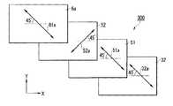
さらに本実施形態の液晶表示装置100では、図4に示すように、第1反射防止フィルム51と第2反射防止フィルム52とが、光軸51aと光軸52aとをほぼ直交させるようにして配置されている。また図4において、第1偏光板6aの偏光軸(透過軸)61aは光軸51a及び光軸52aに対して略45°の角度を成すように配置されている。
なお、図4に示す各光学軸に併記している基準線は、図示のX軸方向に平行な直線である。また、図示X軸方向が液晶表示装置100の略矩形の表示領域の水平方向(又は垂直方向)である。Furthermore, in the liquid
In addition, the reference line written together with each optical axis shown in FIG. 4 is a straight line parallel to the X-axis direction of illustration. The X-axis direction shown in the figure is the horizontal direction (or vertical direction) of the substantially rectangular display area of the liquid
また、本実施形態において液晶パネル2の液晶32は、前面側基板22aに近接する位置において第1偏光板6aの偏光軸61aと平行な配向方向32aを有している。すなわち、前面側基板22aの液晶制御層26aを構成する配向膜の配向方向(例えばラビング方向)が配向方向32aとなっている。
なお、図4では、TNモードの液晶パネル2を想定して配向方向32aを図示しているが、配向方向32aは液晶モード等に応じて異なるので、第1偏光板6aの偏光軸61aと平行でなくても構わない。In the present embodiment, the
In FIG. 4, the
ここで、第1反射防止フィルム51及び第2反射防止フィルム52の光軸51a、52aは、これらを構成する基体50aや反射防止層50bが有するリタデーション(位相差)に基づく、反射防止フィルム全体としての光軸(遅相軸)である。反射防止フィルムや偏光板等の光学フィルムでは、透過光の偏光状態を制御する層以外の層や基体は、リタデーションを有しないものであることが望まれるが、実際にはこれらのリタデーションを完全に無くすことはできず、特に反射防止層50bに比して厚みの大きい基体50aが所定方向の光軸を有する複屈折体となる。 Here, the
そして、このように光軸を有する第1反射防止フィルム51及び第2反射防止フィルム52を、光軸を考慮せずに配置すると、第1反射防止フィルム51及び第2反射防止フィルム52のリタデーションにより液晶パネル2から第1偏光板6aに進行する表示光(偏光)の状態が変化し、コントラストが低下したり、表示が色づいてしまう現象が生じる。 And when the
そこで本発明では、図4に示すように、第1反射防止フィルム51と第2反射防止フィルム52とを、光軸51aと光軸52aとがほぼ直交するように配置し、第1反射防止フィルム51のリタデーションと第2反射防止フィルム52のリタデーションを相殺させるようにしている。つまり、第1反射防止フィルム51の遅相軸である光軸51aに対して、第2反射防止フィルム52の進相軸(光軸52aと直交する軸)が一致するように配置することで、第1反射防止フィルム51と第2反射防止フィルム52とのリタデーションの合計が最小になるようにこれらを配置している。これにより、第1反射防止フィルム51及び第2反射防止フィルム52に起因するコントラスト低下や表示の色づきを防止でき、高画質の表示を得られるようになっている。 Therefore, in the present invention, as shown in FIG. 4, the
また本実施形態において、第1反射防止フィルム51と第2反射防止フィルム52とは、略同一のリタデーションを有するフィルムとすることが好ましい。このような構成とすれば、上述した光軸51a、52aの設定によるリタデーション相殺効果を最大化することができ、第1反射防止フィルム51及び第2反射防止フィルム52に起因するコントラスト低下がほぼ全く生じない液晶表示装置100が得られる。 In the present embodiment, the
以上説明したように、本実施形態の液晶表示装置100では、表示部である液晶パネル2の前面側に配設されたタッチパネル4を透過して液晶パネル2の表示を視認することが可能であるとともに、かかる表示を視認しながらタッチパネル4に対する座標入力操作を行うことができる。
そして、液晶パネル2のタッチパネル4側に接着された第1反射防止フィルム51により基板本体24a表面での光の反射を防止し、さらにタッチパネル4の液晶パネル2側に接着された第2反射防止フィルム52により基板本体11b表面での光の反射を防止することができる。
特に、液晶表示装置100の前面側から入射する外光の反射を防止することができるので、外光反射に起因するコントラストの低下を防止することができ、従来の液晶表示装置に比して高画質で見やすい表示を実現することができる。
さらには、単に反射防止フィルムを設けるのではなく、これらの光学特性を考慮して、これらのフィルムの光軸51a、52aを互いに直交させて配置しているので、反射防止フィルムに起因するコントラスト低下も防止できるようになっている。As described above, in the liquid
Then, the
In particular, since reflection of external light incident from the front side of the liquid
Furthermore, since the
また本発明においては、市販の反射防止フィルムを用いることができる第1反射防止フィルム51及び第2反射防止フィルム52を反射防止構造として採用しているので、基板本体24aや基板本体11aに対する直接の処理が必要である反射防止被膜を採用する場合に比べて、低コストで製造することが可能である。そして、上述した光軸配置によってフィルムのリタデーションによるコントラスト低下を防止し、反射防止被膜を用いた場合と同等の表示特性を備え、かつ安価に提供できる液晶表示装置となっている。 Moreover, in this invention, since the
ところで、本実施形態のように液晶パネル2の前面側にタッチパネル4を設置した構成では、タッチパネル4の表面を指や入力器具3で押圧して入力操作を行なうときに、液晶パネル2の表示に歪みが生じることがある。これは、入力時の押圧力によってタッチパネル4に局所的な変形が生じ、この変形によって、タッチパネル4の背面側に設けた液晶パネル2の前面側基板22aに撓みが生じるためである。この基板の撓みによってセルギャップが局所的に大きく変動し、干渉縞のような歪みが生じる。そこで本実施形態の液晶表示装置100において、液晶パネル2の背面側基板22bの厚みを例えば0.1mm〜0.4mm程度にまで薄くすることが好ましい。このように薄くすることで背面側基板22bが前面側基板22aの撓みに追従しても撓みむようになり、セルギャップの変動を防止することができる。またこの場合において、液晶パネル2の表示領域に対応する背面側基板22bの平面領域に凹部を設けて部分的に薄くしてもよく、かかる凹部に第2偏光板6bを収容して液晶表示装置100全体の薄型化を図ってもよい。 By the way, in the configuration in which the
さらに、タッチパネル4の前面側についても、タッチパネル4の前面側基板8aに凹部を設け、この凹部に第1偏光板6aを収容してもよい。このような構成とすれば、液晶表示装置100全体を薄型化することができる。また偏光板6a、6bは、それぞれ前面側基板8a、背面側基板22bと光学的に接着されていることが好ましい。これらを接着しておくことで、第1偏光板6aと前面側基板8aとの界面、及び第2偏光板6bと背面側基板22bとの界面において光の反射や、干渉を防止することができ、表示品質を向上させることができる。 Furthermore, also on the front side of the
なお図1では、光学フィルムとして第1偏光板6a及び第2偏光板6bのみを示したが、光学フィルムとして1/2波長板や1/4波長板等の位相差板、光学補償板を設置することもできる。さらにこれらの光学フィルムを、偏光板6a、6bとともに基板の凹部に収容することもできる。 Although only the first
また本実施形態の液晶表示装置100において、タッチパネル4の前面側基板8a及び背面側基板8bを構成する基板本体11a、11bには、双方にガラス基板又はプラスチック基板を用いてもよく、操作面側に位置する基板本体11aのみをプラスチック基板としてもよい。前面側の基板本体11aにもガラス基板を用いることで、プラスチック基板を用いる場合よりも入力操作による基板の劣化を生じにくくすることができ、また高温成膜が可能であることから高品質で耐久性に優れた電極を形成できるといった利点が得られる。一方、硬質のガラス基板はプラスチック基板に比べて柔軟性が劣るため、ガラス基板の厚みを0.1mm〜0.2mm程度にまで薄くすることで操作性を確保することが好ましい。 In the liquid
また、タッチパネル4において、前面側基板8a、背面側基板8b、及びシール材9により囲まれた空間に屈折率調整用の液状材料を封入した緩衝構造を用いることもできる。前面側基板8aと背面側基板8bとの間に封入する液状材料としては、ガラスとの屈折率差が空気よりも小さいシリコーンオイル等を用いることが好ましい。液状材料を封入することで、タッチパネル4の内部における界面反射を防止でき、明るく視認性に優れた表示を得られる。また、封入された液状材料が緩衝材として機能し、前面側基板8aに対して衝撃が加わったときに、それを緩和することができ、タッチパネル4の信頼性を向上させることができる。このような緩衝機能を考慮すれば、液状材料の粘度は、例えば2mm2/s〜5000mm2/sの範囲であることが好ましい。In the
(第2の実施形態)
次に、本発明の第2の実施形態について、図5から図9を参照して説明する。
図5は第2実施形態の第1構成例に係る液晶表示装置200の光学軸配置を示す説明図である。図6は、本実施形態の第2構成例に係る液晶表示装置300の光学軸配置を示す説明図である。
なお、本実施形態の液晶表示装置200,300は、第1実施形態に係る液晶表示装置100と共通の構成を備えており、第1反射防止フィルム51と第2反射防止フィルム52の光学軸配置のみが異なっている。また、図5,6に示す各光学軸に併記している基準線は、図示のX軸方向に平行な直線である。また、図示X軸方向が液晶表示装置200,300の略矩形の表示領域の水平方向(又は垂直方向)に一致する。(Second Embodiment)
Next, a second embodiment of the present invention will be described with reference to FIGS.
FIG. 5 is an explanatory diagram showing an optical axis arrangement of the liquid
The liquid
図5に示す第1構成例では、第1偏光板6aの偏光軸61aの配置は第1実施形態と同様であるが、第2反射防止フィルム52の光軸52aが第1偏光板6aの偏光軸61aと略平行に配置されており、第1反射防止フィルム51の光軸51aが第1偏光板6aの偏光軸61aと略直交して配置されている。
一方、図6に示す第2構成例では、第2反射防止フィルム52の光軸52aが第1偏光板6aの偏光軸61aと略直交して配置されており、第1反射防止フィルム51の光軸51aが第1偏光板6aの偏光軸61aと略平行に配置されている。In the first configuration example shown in FIG. 5, the arrangement of the
On the other hand, in the second configuration example shown in FIG. 6, the
図5及び図6に示すように、本実施形態では、第1反射防止フィルム51の光軸51a及び第2反射防止フィルム52の光軸52aが、互いに略直交して配置されるとともに、第1偏光板6aの偏光軸61aに対して略平行に、又は略直交して配置されている。
このような配置形態を採用することで、第1実施形態と比較してもさらに効果的に反射防止フィルムのリタデーションによるコントラスト低下を防止することができる。以下、図7を参照してかかる作用効果について詳細に説明する。As shown in FIGS. 5 and 6, in this embodiment, the
By adopting such an arrangement form, it is possible to more effectively prevent a decrease in contrast due to retardation of the antireflection film even when compared with the first embodiment. Hereinafter, this effect will be described in detail with reference to FIG.
図7は、第2実施形態の液晶表示装置の作用説明図である。図7に示すように、第1偏光板6aの偏光軸61aは、水平方向(X軸方向)に対して45°(135°)の角度を成して配置されている。またこのような偏光軸61aに対して、図5に示す第1構成例では第2反射防止フィルム52の光軸52aが略平行に配置され、図6に示す第2構成例では第1反射防止フィルム51の光軸51aが略平行に配置される。 FIG. 7 is an explanatory diagram of the operation of the liquid crystal display device of the second embodiment. As shown in FIG. 7, the
本実施形態においても、光軸51aと光軸52aとは略直交して配置されているため、先の第1実施形態と同様に、第1反射防止フィルム51と第2反射防止フィルム52は互いのリタデーションを打ち消し合うように作用する。このとき、第1反射防止フィルム51のリタデーションと第2反射防止フィルム52のリタデーション値に差があると、一部のリタデーションが相殺されずに残ってしまう。また、第1反射防止フィルム51と第2反射防止フィルム52とが光軸の直交位置からずれている場合には、第1反射防止フィルム51と第2反射防止フィルム52のリタデーション値が同等であってもリタデーションが残ってしまう。このようにリタデーションが打ち消されずに残ってしまうと、透過光に作用してコントラスト低下や色づきを生じさせる原因となる。 Also in the present embodiment, since the
ところで、光軸51a、52aは互いに略直交して配置されているため、上記の原因により残留するリタデーションは、光軸51a、光軸52aのいずれかと略平行の光軸を有するものとして表れる。すなわち、図7に示す光軸55a又は55bを有する複屈折体とみなすことができる。そうすると、本実施形態の液晶表示装置では、残留するリタデーションに対応する複屈折体の光軸55a、55bは、第1偏光板6aの偏光軸61aに対して略平行又は略直交に配置されることになる。そして、液晶表示装置100における明表示では第1偏光板6aに対して偏光軸61aに略平行の軸を有する偏光が入射し、暗表示では偏光軸61aに対して略直交する軸を有する偏光が入射するので、光軸55a、55bを有する複屈折体は、第1偏光板6aに入射する偏光に対して軸が略平行又は略直交の関係になり、実質的に作用しないものとなる。 By the way, since the
以上から、本実施形態の液晶表示装置200,300では、第1反射防止フィルム51と第2反射防止フィルム52のリタデーションに差がある場合や、第1反射防止フィルム51と第2反射防止フィルム52との光軸が若干ずれている場合であっても、コントラストの低下や色づきを生じさせないようにすることができ、高画質の表示を得ることができる。また、第1反射防止フィルム51と第2反射防止フィルム52との組み合わせの許容範囲が広くなるので、製造性も向上する。 From the above, in the liquid
また、本実施形態の液晶表示装置では、液晶パネルの矩形状の表示領域における水平方向(0°)に対して、第1反射防止フィルム51の光軸51a、及び第2反射防止フィルム52の光軸52aが、いずれも略45°の角度を成して配置されている。このような光学軸配置を採用することで、第1反射防止フィルム51と第2反射防止フィルム52との光軸合わせが容易になり、リタデーションの相殺効果をさらに高めることができる。 In the liquid crystal display device according to the present embodiment, the
具体的には、図5及び図6に示すような第1反射防止フィルム51と第2反射防止フィルム52を用いている場合、これらの反射防止フィルムとして同じく製造されたフィルムを用いることができる。つまり、図8に示すように、同一の大判のフィルム母材150から切り出した第1反射防止フィルム51と第2反射防止フィルム52を1つの液晶表示装置200,300に用いることができる。 Specifically, when the
図8(a)に示すように、大判のフィルム母材150では、基体や反射防止層が同一であるため、切り出した反射防止フィルム51,52の光軸51a、52bは、フィルム母材の光軸150aと一致する同一方向である。そして、このような第1反射防止フィルム51と第2反射防止フィルム52とを、図8(b)に示すように、第2反射防止フィルム52をひっくり返して対向させた状態Pとして液晶表示装置200,300に実装すれば、図5又は図6に示した光学軸配置を容易に得ることができる。 As shown in FIG. 8A, since the base and the antireflection layer are the same in the large format
さらにこの場合において、同一のフィルム母材150から切り出した第1反射防止フィルム51と第2反射防止フィルム52のリタデーションはほぼ同等であるため、第1反射防止フィルム51と第2反射防止フィルム52との重ね合わせによりほぼ完全にリタデーションを相殺することができる。
したがって本実施形態によれば、表示品質に優れ、安価に提供でき、また製造性にも優れた液晶表示装置を実現することができる。Furthermore, in this case, since the retardation of the
Therefore, according to the present embodiment, it is possible to realize a liquid crystal display device that is excellent in display quality, can be provided at low cost, and is excellent in manufacturability.
(第3の実施形態)
次に、本発明の第3の実施形態について図9を参照して説明する。
図9(a)は、第3実施形態の第1構成例である液晶表示装置400Aの模式断面図である。図9(b)は、第3実施形態の第2構成例である液晶表示装置400Bの模式断面図である。(Third embodiment)
Next, a third embodiment of the present invention will be described with reference to FIG.
FIG. 9A is a schematic cross-sectional view of a liquid
図9(a)に示す液晶表示装置400Aは、静電容量方式のタッチパネル(入力装置)4Aを備えている。タッチパネル4Aは、ガラスやプラスチック等からなる支持基板(第3基板)11cを基体として備えており、支持基板11cの一方の面に、平面視ストライプ状の第1ストライプ電極20aと、第1ストライプ電極20aを覆う第1絶縁膜21aと、第1絶縁膜21a上に形成された平面視ストライプ状の第2ストライプ電極20bと、第2ストライプ電極20bを覆う第2絶縁膜21bとが順に形成された構成を備える。タッチパネル4Aの前面側(液晶パネル2と反対側)に第1偏光板6aが接着されており、背面側(液晶パネル2側)には第2反射防止フィルム52が接着されている。 A liquid
液晶パネル2は第1実施形態に係る液晶表示装置100と同様の構成であり、液晶パネル2のタッチパネル4A側の面には第1反射防止フィルム51が接着されている。
そして、第1及び第2実施形態と同様に、第1反射防止フィルム51と第2反射防止フィルム52とは、互いの光軸を略直交させた状態で配置されている。本実施形態においても、第1反射防止フィルム51、第2反射防止フィルム52の光軸51a、52aは、第1偏光板6aの偏光軸61aに対して略平行又は略直交に配置することが好ましい。The
And like 1st and 2nd embodiment, the
上記構成を備えた液晶表示装置400Aは、静電容量式のタッチパネル4Aを透過して液晶パネル2の表示を視認しつつ、タッチパネル4Aによる入力操作を行うことができる。
タッチパネル4Aは、動作時に第1ストライプ電極20a及び第2ストライプ電極20bにそれぞれパルス信号が供給される。このパルス信号の入力により第1ストライプ電極20aと第2ストライプ電極20bの交差部において電極間に静電容量が形成されて作動状態となる。そして、このような状態のタッチパネル4Aに指等が接触すると、電極間の電気力線が指等に吸収されて接触位置に対応する交差部の静電容量が減少する。かかる静電容量の減少を電流変化として検出することで、接触位置を検出することができる。The liquid crystal display device 400 </ b> A having the above configuration can perform an input operation using the
The
このように、液晶パネル2の前面側に配置されるタッチパネルとしては、静電容量方式のものも問題なく用いることができ、かかる構成とした場合にも、先の実施形態の液晶表示装置と同様に、高品質の表示を得ることができ、また安価に提供できるものとなる。 As described above, as the touch panel disposed on the front side of the
次に、図9(b)に示す液晶表示装置400Bは、液晶パネル2の前面側に、タッチパネルではなく透明な板状のカバー部材(第3基板)40を配置した構成である。カバー部材40は、透明なプラスチックやガラスなどからなる基板であり、図示のように筐体60の開口部に固定されていてもよい。カバー部材40の前面側(液晶パネル2と反対側)には第1偏光板6aが接着されており、第1偏光板6aと反対側の面には第2反射防止フィルム52が接着されている。 Next, the liquid
液晶パネル2は第1実施形態に係る液晶表示装置100と同様の構成であり、液晶パネル2のカバー部材40側の面には第1反射防止フィルム51が接着されている。そして、第1及び第2実施形態と同様に、第1反射防止フィルム51と第2反射防止フィルム52とは、互いの光軸を略直交させた状態で配置されている。本実施形態においても、第1反射防止フィルム51、第2反射防止フィルム52の光軸51a、52aは、第1偏光板6aの偏光軸61aに対して略平行又は略直交に配置することが好ましい。 The
このように、液晶パネル2の前面側には電子デバイスに限らず、単なる透明な基板を配置してもよい。かかる構成とした場合にも、先の実施形態の液晶表示装置と同様に、高品質の表示を得ることができ、また安価に提供できるものとなる。 Thus, not only an electronic device but a simple transparent substrate may be disposed on the front side of the
なお、以上の第1から第3の実施形態では、液晶表示装置を挙げて説明したが、本発明の技術範囲はかかる形態に限定されるものではなく、前面側(観察面側)に偏光板が配置される電気光学装置であれば問題なく適用することが可能である。つまり、液晶パネル2に代えて、有機EL表示パネルやプラズマ表示パネル、電気泳動表示パネルなどの電気光学パネルを用いることも可能である。 In the above first to third embodiments, the liquid crystal display device has been described. However, the technical scope of the present invention is not limited to such a form, and a polarizing plate is provided on the front side (observation surface side). Any electro-optical device can be applied without any problem. That is, instead of the
(電子機器)
図10は、本発明に係る電子機器を示す斜視図である。
図10(a)は携帯電話の斜視図である。携帯電話1300は、複数の操作ボタン1302と、受話口1303と、送話口1304と、本発明の液晶表示装置からなる表示部1301とを備えて構成されている。
図10(b)は、他の一例であるハンディターミナル1400を示す斜視図である。ハンディターミナル1400は、本発明の液晶表示装置を用いて構成される表示部1401及びファンクションキー1402、電源スイッチ1403等を備えている。ハンディターミナル1400は、ファンクションキー1402に印刷されたアイコンや、タッチパネル背面の液晶パネル(図示略)の画面を見ながら、タッチパネル上の位置を直接指示することによって、データ入力を行なえるようになっている。
上記構成を備えた携帯電話1300やハンディターミナル1400は、本発明の液晶表示装置を備えているので、外光反射を抑えた高品質の表示部を備えるとともに安価に提供可能な電子機器となる。(Electronics)
FIG. 10 is a perspective view showing an electronic apparatus according to the present invention.
FIG. 10A is a perspective view of a mobile phone. A
FIG. 10B is a perspective view showing a handy terminal 1400 as another example. The
Since the
なお、本発明に係る液晶表示装置を備えた電子機器としては、上記のものに限らず、他に例えば、デジタルカメラ、パーソナルコンピュータ、テレビ、携帯用テレビ、ビューファインダ型・モニタ直視型のビデオテープレコーダ、PDA、携帯用ゲーム機、ページャ、電子手帳、電卓、時計、ワードプロセッサ、ワークステーション、テレビ電話、POS端末、タッチパネルを備えた機器などを挙げることができる。 The electronic apparatus provided with the liquid crystal display device according to the present invention is not limited to the above-mentioned ones. For example, digital cameras, personal computers, televisions, portable televisions, viewfinder type / monitor direct view type video tapes Examples include a recorder, a PDA, a portable game machine, a pager, an electronic notebook, a calculator, a clock, a word processor, a workstation, a videophone, a POS terminal, and a device equipped with a touch panel.
2 液晶パネル、3 入力器具、4,4A タッチパネル、6a 第1偏光板、6b 第2偏光板、8a 前面側基板(第3基板)、8b 背面側基板(第4基板)、11c 支持基板(第3基板)、22a 前面側基板(第1基板)、22b 背面側基板(第2基板)、32 液晶(液晶物質)、50a 基体、50b 反射防止層、50c 接着層、51 第1反射防止フィルム、51a 光軸、52 第2反射防止フィルム、52a 光軸、61a 偏光軸、100,200,300,400A,400B 液晶表示装置 2 liquid crystal panel, 3 input device, 4, 4A touch panel, 6a first polarizing plate, 6b second polarizing plate, 8a front side substrate (third substrate), 8b back side substrate (fourth substrate), 11c supporting substrate (first 3 substrate), 22a front side substrate (first substrate), 22b back side substrate (second substrate), 32 liquid crystal (liquid crystal substance), 50a substrate, 50b antireflection layer, 50c adhesive layer, 51 first antireflection film, 51a optical axis, 52 second antireflection film, 52a optical axis, 61a polarization axis, 100, 200, 300, 400A, 400B liquid crystal display device
Claims (9)
Translated fromJapanese前記第1基板の前記液晶物質と反対側に設けられた偏光板と、
前記第1基板のと前記偏光板との間に設けられた第3基板と、
前記第1基板の前記第3基板側に設けられた第1反射防止部材と、
前記第3基板の前記第1基板側に設けられるとともに前記第1反射防止部材の光軸と略直交する光軸を有する第2反射防止部材と、
を有することを特徴とする液晶表示装置。A first substrate and a second substrate disposed to face each other with a liquid crystal material interposed therebetween;
A polarizing plate provided on the opposite side of the first substrate from the liquid crystal substance;
A third substrate provided between the first substrate and the polarizing plate;
A first antireflection member provided on the third substrate side of the first substrate;
A second antireflection member provided on the first substrate side of the third substrate and having an optical axis substantially orthogonal to the optical axis of the first antireflection member;
A liquid crystal display device comprising:
前記第3基板及び前記第4基板の互いに対向する面にそれぞれ電極が形成され、前記第3基板と前記第4基板とが所定の間隔をもって保持されていることを特徴とする請求項5に記載の液晶表示装置。A fourth substrate is provided between the third substrate and the second antireflection member;
6. The electrode according to claim 5, wherein electrodes are respectively formed on surfaces of the third substrate and the fourth substrate facing each other, and the third substrate and the fourth substrate are held at a predetermined interval. Liquid crystal display device.
Priority Applications (1)
| Application Number | Priority Date | Filing Date | Title |
|---|---|---|---|
| JP2007243431AJP2009075297A (en) | 2007-09-20 | 2007-09-20 | Liquid crystal display and electronic device |
Applications Claiming Priority (1)
| Application Number | Priority Date | Filing Date | Title |
|---|---|---|---|
| JP2007243431AJP2009075297A (en) | 2007-09-20 | 2007-09-20 | Liquid crystal display and electronic device |
Publications (1)
| Publication Number | Publication Date |
|---|---|
| JP2009075297Atrue JP2009075297A (en) | 2009-04-09 |
Family
ID=40610325
Family Applications (1)
| Application Number | Title | Priority Date | Filing Date |
|---|---|---|---|
| JP2007243431APendingJP2009075297A (en) | 2007-09-20 | 2007-09-20 | Liquid crystal display and electronic device |
Country Status (1)
| Country | Link |
|---|---|
| JP (1) | JP2009075297A (en) |
Cited By (3)
| Publication number | Priority date | Publication date | Assignee | Title |
|---|---|---|---|---|
| JP2011081810A (en)* | 2009-10-09 | 2011-04-21 | Lg Chem Ltd | Integrated touch polarizing plate and touch panel including the same |
| WO2012106124A1 (en)* | 2011-02-04 | 2012-08-09 | Guardian Industries Corp. | Electronic devices having reduced susceptibility to newton rings, and/or methods of making the same |
| JP2015122060A (en)* | 2013-11-21 | 2015-07-02 | 大日本印刷株式会社 | Display device with touch panel |
Citations (3)
| Publication number | Priority date | Publication date | Assignee | Title |
|---|---|---|---|---|
| JPH10293292A (en)* | 1997-02-21 | 1998-11-04 | Matsushita Electron Corp | Liquid crystal display device |
| JP2000241794A (en)* | 1999-02-23 | 2000-09-08 | Nissha Printing Co Ltd | Touch input type liquid crystal display device |
| JP2000321558A (en)* | 1999-05-13 | 2000-11-24 | Nissha Printing Co Ltd | Low reflection touch panel |
- 2007
- 2007-09-20JPJP2007243431Apatent/JP2009075297A/enactivePending
Patent Citations (3)
| Publication number | Priority date | Publication date | Assignee | Title |
|---|---|---|---|---|
| JPH10293292A (en)* | 1997-02-21 | 1998-11-04 | Matsushita Electron Corp | Liquid crystal display device |
| JP2000241794A (en)* | 1999-02-23 | 2000-09-08 | Nissha Printing Co Ltd | Touch input type liquid crystal display device |
| JP2000321558A (en)* | 1999-05-13 | 2000-11-24 | Nissha Printing Co Ltd | Low reflection touch panel |
Cited By (8)
| Publication number | Priority date | Publication date | Assignee | Title |
|---|---|---|---|---|
| JP2011081810A (en)* | 2009-10-09 | 2011-04-21 | Lg Chem Ltd | Integrated touch polarizing plate and touch panel including the same |
| WO2012106124A1 (en)* | 2011-02-04 | 2012-08-09 | Guardian Industries Corp. | Electronic devices having reduced susceptibility to newton rings, and/or methods of making the same |
| CN103460118A (en)* | 2011-02-04 | 2013-12-18 | 葛迪恩实业公司 | Electronic device with reduced sensitivity to Newton's rings and/or method of making same |
| JP2014510297A (en)* | 2011-02-04 | 2014-04-24 | ガーディアン・インダストリーズ・コーポレーション | Electronic device with reduced susceptibility to Newton ring and / or manufacturing method thereof |
| CN103460118B (en)* | 2011-02-04 | 2017-07-18 | 葛迪恩实业公司 | Electronic device with reduced sensitivity to Newton's rings and/or method of making same |
| TWI603133B (en)* | 2011-02-04 | 2017-10-21 | 加爾汀工業公司 | Lcd device, electronic devices and methods of making the same, and methods of making a coated artical |
| KR101915334B1 (en)* | 2011-02-04 | 2019-01-14 | 가디언 인더스트리즈 코퍼레이션. | Electronic devices having reduced susceptibility to newton rings, and/or methods of making the same |
| JP2015122060A (en)* | 2013-11-21 | 2015-07-02 | 大日本印刷株式会社 | Display device with touch panel |
Similar Documents
| Publication | Publication Date | Title |
|---|---|---|
| JP4412383B2 (en) | Input device, electro-optical device, and electronic apparatus | |
| CN102473363B (en) | Display device | |
| CN206363696U (en) | Display device | |
| CN107870467B (en) | Display device | |
| JP5413937B2 (en) | Electro-optical device and electronic apparatus | |
| CN100430785C (en) | Input device and manufacturing method thereof, electro-optic device and manufacturing method thereof, electronic device | |
| JP5008026B2 (en) | Display device with input function | |
| JP5520093B2 (en) | Manufacturing method of touch panel | |
| JP5027086B2 (en) | Input device and display device with input function | |
| JP4802778B2 (en) | Input device, electro-optical device and electronic apparatus | |
| JP2013168172A (en) | Slim type touch device | |
| JP2019101095A (en) | Liquid crystal panel | |
| TWI464482B (en) | Input device, electro-optical device and electronic machine | |
| US12124137B2 (en) | Display device | |
| JP5255876B2 (en) | Liquid crystal display device and electronic apparatus using the same | |
| JP2019191460A (en) | Display device | |
| JP5306718B2 (en) | Liquid crystal display device and electronic device | |
| US20170249046A1 (en) | Liquid crystal display device, wiring substrate, and sensor-equipped display device | |
| JP2009075297A (en) | Liquid crystal display and electronic device | |
| JP4539533B2 (en) | Electro-optical device and electronic apparatus | |
| JP2007065855A (en) | Display device with touch panel | |
| JP2019101548A (en) | Liquid crystal panel | |
| JP2008026584A (en) | Electro-optical device and electronic apparatus | |
| JP3708698B2 (en) | Liquid crystal display device with input device and electronic device | |
| TWI416383B (en) | Touch panel and liquid crystal display panel |
Legal Events
| Date | Code | Title | Description |
|---|---|---|---|
| A621 | Written request for application examination | Free format text:JAPANESE INTERMEDIATE CODE: A621 Effective date:20100309 | |
| A711 | Notification of change in applicant | Free format text:JAPANESE INTERMEDIATE CODE: A711 Effective date:20100526 | |
| RD02 | Notification of acceptance of power of attorney | Free format text:JAPANESE INTERMEDIATE CODE: A7422 Effective date:20100526 | |
| A521 | Written amendment | Free format text:JAPANESE INTERMEDIATE CODE: A523 Effective date:20100630 | |
| A977 | Report on retrieval | Free format text:JAPANESE INTERMEDIATE CODE: A971007 Effective date:20120125 | |
| A131 | Notification of reasons for refusal | Free format text:JAPANESE INTERMEDIATE CODE: A131 Effective date:20120207 | |
| A711 | Notification of change in applicant | Free format text:JAPANESE INTERMEDIATE CODE: A711 Effective date:20120330 | |
| A521 | Written amendment | Free format text:JAPANESE INTERMEDIATE CODE: A523 Effective date:20120402 | |
| A02 | Decision of refusal | Free format text:JAPANESE INTERMEDIATE CODE: A02 Effective date:20120710 |