JP2009071133A - Plasma processing apparatus and plasma processing method - Google Patents
Plasma processing apparatus and plasma processing methodDownload PDFInfo
- Publication number
- JP2009071133A JP2009071133AJP2007239372AJP2007239372AJP2009071133AJP 2009071133 AJP2009071133 AJP 2009071133AJP 2007239372 AJP2007239372 AJP 2007239372AJP 2007239372 AJP2007239372 AJP 2007239372AJP 2009071133 AJP2009071133 AJP 2009071133A
- Authority
- JP
- Japan
- Prior art keywords
- electrode
- voltage
- frequency
- power supply
- plasma
- Prior art date
- Legal status (The legal status is an assumption and is not a legal conclusion. Google has not performed a legal analysis and makes no representation as to the accuracy of the status listed.)
- Granted
Links
Images


Classifications
- H—ELECTRICITY
- H01—ELECTRIC ELEMENTS
- H01L—SEMICONDUCTOR DEVICES NOT COVERED BY CLASS H10
- H01L21/00—Processes or apparatus adapted for the manufacture or treatment of semiconductor or solid state devices or of parts thereof
- H01L21/02—Manufacture or treatment of semiconductor devices or of parts thereof
- H01L21/04—Manufacture or treatment of semiconductor devices or of parts thereof the devices having potential barriers, e.g. a PN junction, depletion layer or carrier concentration layer
- H01L21/18—Manufacture or treatment of semiconductor devices or of parts thereof the devices having potential barriers, e.g. a PN junction, depletion layer or carrier concentration layer the devices having semiconductor bodies comprising elements of Group IV of the Periodic Table or AIIIBV compounds with or without impurities, e.g. doping materials
- H01L21/30—Treatment of semiconductor bodies using processes or apparatus not provided for in groups H01L21/20 - H01L21/26
- H01L21/31—Treatment of semiconductor bodies using processes or apparatus not provided for in groups H01L21/20 - H01L21/26 to form insulating layers thereon, e.g. for masking or by using photolithographic techniques; After treatment of these layers; Selection of materials for these layers
- H01L21/3105—After-treatment
- H01L21/311—Etching the insulating layers by chemical or physical means
- H01L21/31105—Etching inorganic layers
- H01L21/31111—Etching inorganic layers by chemical means
- H01L21/31116—Etching inorganic layers by chemical means by dry-etching
- H—ELECTRICITY
- H01—ELECTRIC ELEMENTS
- H01J—ELECTRIC DISCHARGE TUBES OR DISCHARGE LAMPS
- H01J37/00—Discharge tubes with provision for introducing objects or material to be exposed to the discharge, e.g. for the purpose of examination or processing thereof
- H01J37/32—Gas-filled discharge tubes
- H01J37/32009—Arrangements for generation of plasma specially adapted for examination or treatment of objects, e.g. plasma sources
- H01J37/32082—Radio frequency generated discharge
- H01J37/32091—Radio frequency generated discharge the radio frequency energy being capacitively coupled to the plasma
- H—ELECTRICITY
- H01—ELECTRIC ELEMENTS
- H01J—ELECTRIC DISCHARGE TUBES OR DISCHARGE LAMPS
- H01J37/00—Discharge tubes with provision for introducing objects or material to be exposed to the discharge, e.g. for the purpose of examination or processing thereof
- H01J37/32—Gas-filled discharge tubes
- H01J37/32009—Arrangements for generation of plasma specially adapted for examination or treatment of objects, e.g. plasma sources
- H01J37/32082—Radio frequency generated discharge
- H01J37/32137—Radio frequency generated discharge controlling of the discharge by modulation of energy
- H01J37/32155—Frequency modulation
- H01J37/32165—Plural frequencies
Landscapes
- Engineering & Computer Science (AREA)
- Chemical & Material Sciences (AREA)
- Physics & Mathematics (AREA)
- Plasma & Fusion (AREA)
- Analytical Chemistry (AREA)
- Condensed Matter Physics & Semiconductors (AREA)
- General Chemical & Material Sciences (AREA)
- Inorganic Chemistry (AREA)
- Chemical Kinetics & Catalysis (AREA)
- General Physics & Mathematics (AREA)
- Manufacturing & Machinery (AREA)
- Computer Hardware Design (AREA)
- Microelectronics & Electronic Packaging (AREA)
- Power Engineering (AREA)
- Plasma Technology (AREA)
- Drying Of Semiconductors (AREA)
- Chemical Vapour Deposition (AREA)
Abstract
Translated fromJapaneseDescription
Translated fromJapanese本発明は、半導体装置等の製造プロセスに用いられるプラズマ処理装置およびプラズマ処理方法に関する。 The present invention relates to a plasma processing apparatus and a plasma processing method used in a manufacturing process of a semiconductor device or the like.
近時、半導体デバイスの高性能化,高集積化および微細化が急速に進んでいる。半導体デバイスの高集積化のためには、微細加工技術,エピタキシャル成長技術,パッケージング技術等の向上が必要となるが、中でも微細加工技術の比重が高く、高アスペクト比や最小線幅の狭小化等の加工精度の向上が強く求められている。 Recently, high performance, high integration and miniaturization of semiconductor devices are rapidly progressing. High integration of semiconductor devices requires improvements in microfabrication technology, epitaxial growth technology, packaging technology, etc. Among them, microfabrication technology has a high specific gravity, high aspect ratio, narrowing of minimum line width, etc. There is a strong demand for improved machining accuracy.
このような半導体デバイスの微細加工技術の1つとして、高いエッチングレートで異方性微細加工が可能な反応性イオンエッチング(Reactive Ion Etching;RIE)が知られている。一般的にRIEでは、雰囲気調整が可能なチャンバ内に一対の電極を所定間隔で対向配置し、一方の電極に基板を保持させ、電極に高周波電力(RF電力)を供給して電極間にプラズマを生成させる。 As one of such microfabrication techniques for semiconductor devices, reactive ion etching (RIE) capable of anisotropic microfabrication at a high etching rate is known. In general, in RIE, a pair of electrodes are arranged opposite to each other at a predetermined interval in a chamber capable of adjusting the atmosphere, a substrate is held on one electrode, high frequency power (RF power) is supplied to the electrodes, and plasma is generated between the electrodes. Is generated.
RIEは、このとき基板に生じる自己バイアス電圧とプラズマポテンシャルの差の電位によってプラズマ中の正イオンが加速されて基板に入射し衝突する物理的エッチング(スパッタリング)と、活性な中性ラジカルによる化学的エッチングの複合作用を利用する。プラズマポテンシャルは自己バイアス電圧よりも相対的に小さいために、基板に入射するイオンのエネルギー制御は自己バイアス電圧を制御することによって行われている。 In RIE, physical etching (sputtering) in which positive ions in the plasma are accelerated by the potential of the difference between the self-bias voltage generated on the substrate and the plasma potential at this time and incident on the substrate and collide with it, and chemical by active neutral radicals. Utilizes the combined action of etching. Since the plasma potential is relatively smaller than the self-bias voltage, the energy control of ions incident on the substrate is performed by controlling the self-bias voltage.
電極電位はRF電圧に対応して周期的に変化するため、イオンエネルギーも周期的に変化する。そして、イオンエネルギーはRF電圧の周波数に依存して分散し、RF電圧の周波数が低いほどイオンエネルギーの分散は大きくなることが知られている。 Since the electrode potential changes periodically corresponding to the RF voltage, the ion energy also changes periodically. It is known that the ion energy is dispersed depending on the frequency of the RF voltage, and the dispersion of the ion energy increases as the frequency of the RF voltage decreases.
イオンエネルギーに分散が生じると、高エネルギーのイオンは肩削りを誘発して加工形状を悪化させ、一方、低エネルギーのイオンは基板加工に寄与せずまたは異方性劣化に伴い加工形状を悪化させるおそれがある。そこで、プラズマを生成、維持するためのRF電力とイオンエネルギーを制御するためのRF電力の2つ以上の異なる周波数のRF電力を用いる技術が提案されている(例えば、特許文献1参照)。 When dispersion occurs in ion energy, high-energy ions induce shoulder cutting and deteriorate the processing shape, while low-energy ions do not contribute to substrate processing or deteriorate the processing shape due to anisotropic deterioration. There is a fear. Therefore, a technique has been proposed that uses RF power of two or more different frequencies of RF power for generating and maintaining plasma and RF power for controlling ion energy (see, for example, Patent Document 1).
しかしながら、このような従来技術では、低い周波数に起因するイオンエネルギーの分散が大きく、この分散を加工精度の向上のために必要とされる範囲に十分に狭帯域化させることは困難である。また、低い方の周波数を高くすることでイオンエネルギーの分散を小さくすることができるが、所望されるイオンエネルギーを得ることが困難になるという問題がある。
本発明は、プラズマ中のイオンに基板の処理に適したエネルギーをもたせるとともに、イオンエネルギーの分散を狭帯域化させることを可能とするプラズマ処理装置およびプラズマ処理方法を提供することを目的とする。 An object of the present invention is to provide a plasma processing apparatus and a plasma processing method capable of giving ions suitable for processing a substrate to ions in plasma and narrowing the dispersion of ion energy.
本発明は第1態様として、被処理基板を載置する第1電極と、
一定間隔で前記第1電極と対向するように配置された第2電極と、
前記第1,第2電極を収容し、その内部の雰囲気を調整可能に構成されたチャンバと、
前記第1電極上の自己バイアス電圧を制御するための電圧を、所定の第1周波数のRF電圧のピーク−ピーク電圧のうちの略一定幅かつ略一定値により、間欠的に前記第1電極に印加する第1電源装置と、
前記第1,第2電極間にプラズマを発生させるための所定の第2周波数のRF電圧を、連続的にまたは前記第1電源装置から出力される電圧と同期させて間欠的に、前記第1電極または前記第2電極に印加する第2電源装置と、を具備することを特徴とするプラズマ処理装置を提供する。As a first aspect of the present invention, a first electrode on which a substrate to be processed is placed;
A second electrode arranged to face the first electrode at regular intervals;
A chamber configured to accommodate the first and second electrodes, and to be capable of adjusting an atmosphere inside the first and second electrodes;
A voltage for controlling the self-bias voltage on the first electrode is intermittently applied to the first electrode according to a substantially constant width and a substantially constant value of a peak-peak voltage of an RF voltage having a predetermined first frequency. A first power supply to be applied;
An RF voltage having a predetermined second frequency for generating plasma between the first and second electrodes is continuously or intermittently synchronized with a voltage output from the first power supply device. And a second power supply device applied to the electrode or the second electrode.
本発明は第2態様として、被処理基板を載置する第1電極と、
一定間隔で前記第1電極と対向するように配置された第2電極と、
前記第1,第2電極を収容し、その内部の雰囲気を調整可能に構成されたチャンバと、
前記第1電極上の自己バイアス電圧を制御するための所定の第1周波数の直流パルス電圧を前記第1電極に印加する第1電源装置と、
前記第1,第2電極間にプラズマを発生させるための所定の第2周波数のRF電圧を前記直流パルス電圧と同期させて前記第1電極または前記第2電極に印加する第2電源装置と、を具備することを特徴とするプラズマ処理装置を提供する。As a second aspect of the present invention, a first electrode on which a substrate to be processed is placed;
A second electrode arranged to face the first electrode at regular intervals;
A chamber configured to accommodate the first and second electrodes, and to be capable of adjusting an atmosphere inside the first and second electrodes;
A first power supply device that applies a DC pulse voltage having a predetermined first frequency to control the self-bias voltage on the first electrode to the first electrode;
A second power supply device that applies an RF voltage of a predetermined second frequency for generating plasma between the first and second electrodes to the first electrode or the second electrode in synchronization with the DC pulse voltage; A plasma processing apparatus is provided.
本発明は第3態様として、その内部雰囲気を調整可能に構成されたチャンバ内の下部および上部に互いに一定間隔で対向するようにそれぞれ配置された第1電極と第2電極の当該第1電極上に被処理基板を載置させ、
前記第1電極上の自己バイアス電圧を制御するための電圧を、所定の第1周波数のRF電圧のピーク−ピーク電圧のうちの略一定幅かつ略一定値により、間欠的に前記第1電極に印加するとともに、前記第1,第2電極間にプラズマを発生させるための所定の第2周波数のRF電圧を連続的にまたは前記第1電極に印加される電圧と同期させて間欠的に前記第1電極または前記第2電極に印加し、
或いは、前記第1電極上の自己バイアス電圧を制御するための所定の直流パルス電圧を前記第1電極に印加するとともに、前記第1,第2電極間にプラズマを発生させるための所定のRF電圧を前記直流パルス電圧と同期させて間欠的に前記第1電極または前記第2電極に印加することを特徴とするプラズマ処理方法を提供する。According to a third aspect of the present invention, there is provided a first electrode and a second electrode arranged on the first electrode and the second electrode, respectively, which are arranged so as to face each other at a predetermined interval in a lower part and an upper part in a chamber configured to be capable of adjusting the internal atmosphere. Place the substrate to be processed on
A voltage for controlling the self-bias voltage on the first electrode is intermittently applied to the first electrode according to a substantially constant width and a substantially constant value of a peak-peak voltage of an RF voltage having a predetermined first frequency. And applying an RF voltage having a predetermined second frequency for generating plasma between the first and second electrodes continuously or in synchronization with a voltage applied to the first electrode. Applied to one electrode or the second electrode;
Alternatively, a predetermined DC pulse voltage for controlling a self-bias voltage on the first electrode is applied to the first electrode, and a predetermined RF voltage for generating plasma between the first and second electrodes Is intermittently applied to the first electrode or the second electrode in synchronization with the DC pulse voltage.
本発明によれば、プラズマ中のイオンに基板の処理に適したエネルギーをもたせるとともに、イオンエネルギーの分散を狭帯域化することができ、これによりプラズマを用いた種々の加工を高精度に行うことができる。 According to the present invention, the ions in the plasma can have energy suitable for the processing of the substrate, and the dispersion of the ion energy can be narrowed, whereby various processing using the plasma can be performed with high accuracy. Can do.
以下、本発明の実施の形態について図面を参照しながら詳細に説明する。ここではプラズマ処理装置として、半導体基板(以下「基板」と記す)にRIE処理を施すRIEプラズマ処理装置(以下「RIE装置」と記す)を取り上げることとする。 Hereinafter, embodiments of the present invention will be described in detail with reference to the drawings. Here, as the plasma processing apparatus, an RIE plasma processing apparatus (hereinafter referred to as “RIE apparatus”) that performs RIE processing on a semiconductor substrate (hereinafter referred to as “substrate”) is taken up.
図1に本発明の第1形態に係るRIE装置10Aの概略構成を示す。RIE装置10Aは、基板Wを載置する第1電極たる高周波電極(以下「RF電極」と記す)11と、一定間隔でこのRF電極11と対向するように配置された第2電極たる対向電極12と、これらRF電極11と対向電極12を収容するチャンバ13と、チャンバ13の内部にプラズマ生成に必要なガスを供給するためのガス供給機構14と、チャンバ13内を減圧するための減圧ポンプ15を備えている。 FIG. 1 shows a schematic configuration of an
ガス供給機構14からチャンバ13の内部へ供給されるガスとしては、Ar,Kr,Xe,N2,O2,CO,H2等のガスの他、SF6やCF4,C2F6,C4F8,C5F8,C4F6,Cl2,HBr,SiH4,SiF4等のプロセスガスが挙げられる。対向電極12はこれらのガスをチャンバ13の内部に送出する構造となっている。ガス供給機構14と減圧ポンプ15の動作調節により、チャンバ13の内部を所望する処理雰囲気、例えば1Pa〜数Paに調整することができるようになっている。Gases supplied from the
ガス供給機構14からチャンバ13内に供給されるガスをRF電極11と対向電極12の間でプラズマ化させてRIE処理を行うために、RIE装置10Aは、RF電極11に異なる周波数の高周波(RF)電圧を印加する第1電源装置18と第2電源装置19を備えている。なお、RF電極11の詳細な構造は図1に示していないが、RF電極11は、例えば基板Wを吸着保持するための静電チャックと、この静電チャックを支持する金属製のステージから構成されており、このステージにRF電圧が印加される。静電チャックには基板Wを所定温度に保持するためのヒータを埋設することができる。対向電極12はアース(グランド)電位に保持されている。 In order to perform the RIE process by making the gas supplied from the
第1電源装置18は、RF電極11上の自己バイアス電圧(つまりRF電極11に保持された基板Wに生じる自己バイアス電圧)Vdcを制御するための電圧を間欠的にRF電極11に印加する。そのために第1電源装置18は、第1周波数f1でsin波形のRF電圧を連続的に出力する第1RF電源21と、プラズマ負荷に対するインピーダンス整合等を行う第1整合器22と、第1RF電源21から出力されるRF電圧を周期的にアース側へ逃がすための第1スイッチング部23を備えている。第1電源装置18はまた、第2電源装置19からRF電極11へ供給される電力成分が第1整合器22へ侵入することを防止するための第1フィルタ24を備えている。The first
第2電源装置19は、RF電極11と対向電極12の間にプラズマを発生させ、これを維持することを主目的とするRF電圧をRF電極11に印加する。そのために第2電源装置19は、第2周波数f2のRF電圧を連続的に出力する第2RF電源25と、第2整合器26と、第1電源装置18からRF電極11に供給される電力成分が第2整合器26へ侵入することを防止するための第2フィルタ27を備えている。The second
第2周波数f2は、例えば100MHzに設定される。第1周波数f1は第2周波数f2よりも低い周波数に設定され、例えば1MHzや13.56MHzに設定することができる。その設定条件については後に詳細に説明する。The second frequencyf 2 is set to, for example, 100 MHz. The first frequencyf 1 may be set at a frequency lower than the second frequencyf 2, for example, 1MHz or 13.56 MHz. The setting conditions will be described in detail later.
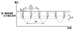
図2に第1電源装置18と第2電源装置19からそれぞれ出力される電圧波形およびこれらの重畳電圧波形を模式的に示す。第1スイッチング部23は、RF電極11に対して、時間幅t0での電圧印加の間に時間幅t1の無電圧時間が存在するように、スイッチング動作を行う。つまり、第1スイッチング部23は第1RF電源21から出力される電圧をパルス化する。FIG. 2 schematically shows voltage waveforms output from the first
時間幅t0,t1は1/f1=t0+t1の関係を満たしている。したがって図2上段の波形に示されるように、第1RF電源21から出力される第1周波数f1のRF電圧のピーク−ピーク電圧V1P−Pのうちの略一定幅(電位差ΔV)かつ略一定値が、間欠的にRF電極11に印加されることとなる。The time widths t0 and t1 satisfy the
“略一定幅”,“略一定値”とは、その幅,絶対値に、第1スイッチング部23の動作精度等に依存して若干のばらつきが生じることがあることをいう。理想的な状態では、図2上段の波形に示される通り、RF電圧の変化に対して時間幅t0,t1は時間的にずれることなく、したがって電位差ΔVの幅は変化することなく、かつ、印加電圧の絶対値は一定値内に維持される。以下、このようにして第1電源装置18から出力される電圧を“第1周波数f1のパルス電圧”ということとする。“Substantially constant width” and “substantially constant value” mean that the width and absolute value may vary slightly depending on the operation accuracy of the
第1周波数f1のパルス電圧は、負の自己バイアス電位によって負の電圧値領域で変化するようになるため、第1周波数f1のパルス電圧を正電圧としてしまうと、自己バイアス電圧Vdcの絶対値が小さくなる。そこで、第1周波数f1のパルス電圧は負のパルス電圧とする。Since the pulse voltage of the first frequency f1 changes in the negative voltage value region due to the negative self-bias potential, if the pulse voltage of the first frequency f1 is set to a positive voltage, the self-bias voltage Vdc The absolute value becomes smaller. Therefore, the pulse voltage of the first frequency f1 is a negative pulse voltage.
第2電源装置19からは、図2中段の電圧波形に示されるように、第2周波数f2のRF電圧が連続的に出力される。第1RF電源21から出力されるRF電圧のピーク−ピーク電圧V1P−Pは数百ボルトとされるのに対して、第2RF電源25から出力されるRF電圧のピーク−ピーク電圧V2P−Pは数十ボルトとされ、これらはともに負電圧とされる。そのため第1電源装置18から出力される第1周波数f1のパルス電圧と第2電源装置19から出力される第2周波数f2のRF電圧とが重畳されると、図2下段に示されるような電圧波形が得られる。From the second
この図2下段に示した重畳電圧がRF電極11に印加されることによってRF電極11と対向電極12との間に生じるプラズマの電子密度Neと,プラズマポテンシャルVPと,自己バイアス電圧Vdcの関係を模式的に図3に示す。And the electron density Ne of the plasma generated between the
プラズマ電子密度Neは、第2電源装置19からRF電極11に印加される第2周波数f2のRF電力成分に依存するため、ほぼ一定値に維持される。したがって、プラズマ中の正イオン密度も一定に維持され(図示せず)、プラズマポテンシャルVPも一定に維持される。Plasma electron density Ne is dependent on the RF power components of the second frequency f2 which is applied from the second
自己バイアス電圧Vdcは、実質的に第1周波数f1のパルス電圧の変化に対応して負の電圧値範囲において変化し、第2周波数f2のRF電圧の寄与は無視することができる。自己バイアス電圧Vdcは負電位であり、プラズマポテンシャルVPは正電位であるから、プラズマ中の正イオンのイオンエネルギーEiは自己バイアス電圧VdcとプラズマポテンシャルVPとの差(すなわち絶対値の和)で表される。プラズマポテンシャルVPは自己バイアス電圧Vdcに比べて極めて小さいために、実質的に自己バイアス電圧VdcをイオンエネルギーEiと考えることができる。The self-bias voltage Vdc changes in the negative voltage value range substantially corresponding to the change in the pulse voltage at the first frequency f1 , and the contribution of the RF voltage at the second frequency f2 can be ignored. Self-bias voltage Vdc is negative potential, because the plasma potential VP is the positive potential, the ion energy Ei of the positive ions in the plasma difference between the self-bias voltage Vdc and plasma potential VP (i.e. absolute value Sum). Plasma potential VP is for very small compared to the self-bias voltage Vdc, substantially self-bias voltage Vdc can be considered as the ion energy Ei.
そこで、RF電極11への小さな電力投入によってプラズマ中の正イオンにRIE加工に必要なエネルギーを持たせるために、先に図2上段に示した通り、時間幅t0の中央(=t0/2)において第1周波数f1のsin波RF電圧値が極小値をとるように時間幅t0,t1が設定された第1周波数f1のパルス電圧を用いる。これにより、図3に示されるように、絶対値の大きな自己バイアス電圧Vdcを生じさせてプラズマ中の正イオンを加速させ、基板Wに引き込むことができる。Therefore, in order to give positive ions in the plasma energy necessary for RIE processing by applying a small electric power to the
第1周波数f1のパルス電圧における電位差ΔVに起因して、自己バイアス電圧Vdcには電位差ΔVdcが生じる。この電位差ΔVdcはイオンエネルギーEiの分散(分布幅)を広くする1つの要因となる。図2に示した通りに時間幅t0の中央(=t0/2)で第1周波数f1のsin波RF電圧値が極小値をとるように時間幅t0,t1を設定することにより、時間幅t0に対する電位差ΔVを最も小さくすることができ、これにより電位差ΔVdcを小さく抑えることができる。イオンエネルギーEiの分散を狭帯域化するために、時間幅t0は第1周波数f1の周期(=1/f1)の1/4周期以下とすることが望ましい。Due to the potential difference ΔV in the pulse voltage of the first frequency f1, a potential difference ΔVdc is generated in the self-bias voltage Vdc . This potential difference ΔVdc is one factor that widens the dispersion (distribution width) of the ion energy Ei . Central durationt 0 as shown in FIG. 2(= t 0/2) by sin wave RF voltage value of the first frequencyf 1 is set the
イオンエネルギーEiの分散は、プラズマ中の正イオンがRF電極11の電極電位に追従できるか否かにも依存する。プラズマ中の正イオンは、RF電極11の電極電位の周波数がプラズマのイオン周波数ωpi以下である場合に、この電極電位に追従する。ここで、ωpi=(e2Ni/(ε0M))1/2[Hz](但し、Ni:イオン密度(個/m3)、ε0:真空の誘電率、M:イオン質量(kg)、e:電子素量)で与えられる。The dispersion of the ion energy Ei also depends on whether or not positive ions in the plasma can follow the electrode potential of the
RF電極11の電極電位の周波数は第1周波数f1と同じであるから、第1周波数f1がイオン周波数ωpi以下である場合に、プラズマ中の正イオンはRF電極11の電極電位に追従したイオンエネルギーを有するようになる。図3の自己バイアス電圧Vdcはこのイオンエネルギーを反映する値を示す。Since the frequency of the electrode potential of the
第1比較例として、RIE装置10Aから第1スイッチング部23を取り除いた構成のRIE装置を用い、第1周波数f1(=1MHz)のRF電圧と第2周波数f2(=100MHz)のRF電圧を連続的にRF電極11に重畳印加した場合のイオンエネルギーの分布を、連続体モデルプラズマシミュレータ(G. Chen, L.L. Raja, J. Appl. Phys., 96, 6073(2004))でシミュレーションした結果を図4に模式的に示す。As a first comparative example, an RIE apparatus having a configuration in which the
また第1実施例として、RIE装置10Aを用い、第1周波数f1(=1MHz)のパルス電圧(時間幅t0=1/4f1)と第2周波数f2(=100MHz)の連続RF電圧を、第1比較例と同電圧,同電力でRF電極11に重畳印加した場合のイオンエネルギーの分布を、同シミュレータにより求めた結果を図4に模式的に併記する。ここで、具体的に図4においては、RF電極と対向電極の電極間距離を30mm、基板サイズをφ300mm、アルゴン(Ar)ガス流量を200sccm、チャンバ圧力を1.333Pa(=10mTorr)とし、第1周波数f1(=1MHz)のRF電圧(VP−P=900V,電力:400W)と第2周波数f2(=100MHz)のRF電圧(VP−P=20V,電力:500W)をRF電極11に重畳印加した場合のイオンエネルギーの分布を示している。なお、図4では第1比較例と第1実施例の各イオンエネルギー分布を、ベースラインを上下にずらして記載している。As a first example, using a
先に示した種々のガスを用いたプラズマ中の正イオンは、RF電極11の電極電位が周波数1MHzで変化する場合にこの電極電位に追従する。第1比較例の場合には、プラズマ中のイオンエネルギーは低エネルギー側ピークと高エネルギー側ピークに分かれており、そのエネルギー差は約700eVである。また、これら2つのピーク間のエネルギーを有するイオンが一定の割合で存在している。これに対して、第1実施例の場合には、低エネルギー側ピークと高エネルギー側ピークとの間のエネルギー差は第1比較例の場合と同等であるが、高エネルギー側ピークは、狭いピーク幅を有しながら極端に大きくなっており、このピークのエネルギーを有するイオンの割合が極めて多くなっていることがわかる。この高エネルギー側ピークが全体に占める割合は80%程度にまで達する。 The positive ions in the plasma using the various gases described above follow this electrode potential when the electrode potential of the
よって、この高エネルギー側ピーク位置を適切なエネルギー範囲内に設定し、実質的にこの高エネルギー側ピークを専ら用いて基板WのRIE処理を行うことにより、加工形状を精密に制御することができるようになる。この高エネルギー側ピークの値は第1周波数f1のパルス電圧の値により制御することができる。Therefore, the processing shape can be precisely controlled by setting the high energy side peak position within an appropriate energy range and substantially performing the RIE processing of the substrate W using the high energy side peak. It becomes like this. The value of the high-energy side peak can be controlled by the value of the first frequency f1 of the pulse voltage.
一方、RF電極11の電極電位の周波数がプラズマのイオン周波数ωpi超である場合には、プラズマ中の正イオンはこの電極電位に追従することができない。この場合、イオンエネルギーすなわち自己バイアス電圧Vdcは、第1周波数f1のパルス電圧の値よりも小さい振幅で変動する。On the other hand, when the frequency of the electrode potential of the
第2比較例として、RIE装置10Aから第1スイッチング部23を取り除いたRIE装置の構成において、RF電極と対向電極の電極間距離を30mm、基板サイズをφ300mm、アルゴン(Ar)ガス流量を200sccm、チャンバ圧力を1.333Pa(=10mTorr)とし、第1周波数f1(=13.56MHz)のRF電圧(VP−P=900V,電力:400W)と第2周波数f2(=100MHz)のRF電圧(VP−P=20V,電力:500W)を連続的にRF電極11に重畳印加した場合のイオンエネルギーの分布を、前記シミュレータでシミュレーションした結果を図5に示す。As a second comparative example, in the configuration of the RIE apparatus in which the
これに対して、第2実施例としてRIE装置10Aを用い、第1周波数f1(=13.56MHz)のパルス電圧(時間幅t0=1/4f1)と、第2周波数f2(=100MHz)の連続RF電圧を、第2比較例と同電圧,同電力でRF電極11に重畳印加した場合のイオンエネルギーの分布を、同シミュレータにより求めた結果を図5に模式的に併記する。さらに図5に、RF電極11に100MHzのRF電圧のみを第2実施例と同電圧,同電力で連続印加した場合のイオンエネルギーを併記する。On the other hand, using the
先に示した種々のガスを用いたプラズマ中の正イオンは、RF電極11の電極電位が周波数13.56MHzで変化する場合には、この電極電位に追従することができない。 The positive ions in the plasma using the various gases described above cannot follow the electrode potential when the electrode potential of the
第2比較例では自己バイアス電圧Vdcとして−350Vが発生し、イオンエネルギーは320eV〜450eVで、イオンエネルギーの分散ΔE1は130eVとなっている。この場合、一部の正イオンはRIE加工に適したエネルギー範囲から外れたエネルギーを有してしまうこととなる。In the second comparative example, −350 V is generated as the self-bias voltage Vdc , the ion energy is 320 eV to 450 eV, and the ion energy dispersion ΔE1 is 130 eV. In this case, some of the positive ions have energy that is out of the energy range suitable for RIE processing.
これに対して第2実施例では、第2比較例と同様に自己バイアス電圧Vdcとして−350Vが得られる。また、第1周波数f1のパルス電圧に正イオンが追従できないために、低エネルギー側ピークと高エネルギー側ピークとが近接するようになり、イオンエネルギーの分散ΔE2は40eVとなって、第2比較例の場合の約1/3に狭帯域化される。これにより、実質的に全ての正イオンのイオンエネルギーをRIE加工に適したエネルギー範囲に収めることができる。On the other hand, in the second embodiment, −350 V is obtained as the self-bias voltage Vdc as in the second comparative example. Further, since positive ions cannot follow the pulse voltage of the first frequency f1 , the low energy side peak and the high energy side peak come close to each other, and the ion energy dispersion ΔE2 becomes 40 eV, The bandwidth is narrowed to about 1/3 of the comparative example. Thereby, the ion energy of substantially all the positive ions can be within the energy range suitable for RIE processing.
なお、第2周波数f2(=100MHz)のRF電圧だけがRF電極11に印加された場合のイオンエネルギーは約75eVで、このイオンエネルギーを有する正イオンはRIE加工に寄与しない。Note that the ion energy when only the RF voltage of the second frequency f2 (= 100 MHz) is applied to the
第1実施例と第2実施例とを対比すると、第1実施例によるイオンエネルギーの狭帯域化では、多くのイオンが高エネルギー部に集中する一方で、一定量のイオンはこれよりも低いエネルギーを有し、その分布範囲も広いことから、このような低エネルギーのイオンが加工形状を悪化させるおそれや、エッチングレートを高めることを困難にするおそれがないとは言えない。 When comparing the first embodiment with the second embodiment, in the narrowing of the ion energy band according to the first embodiment, while many ions are concentrated in the high energy part, a certain amount of ions has a lower energy. Since the distribution range is wide, it cannot be said that there is no risk that such low-energy ions may deteriorate the processed shape or make it difficult to increase the etching rate.
これに対して、第2実施例では、プラズマ中のほぼ全ての正イオンがRIE加工に適したイオンエネルギーを有するように、イオンエネルギーの分散を狭帯域化させることができるので、高いエッチングレートと高精度な加工を同時に実現することができる。 On the other hand, in the second embodiment, since the dispersion of ion energy can be narrowed so that almost all positive ions in the plasma have ion energy suitable for RIE processing, a high etching rate can be obtained. High precision machining can be realized at the same time.
次に、このようなイオンエネルギーの狭帯域化がRIE加工プロセスに及ぼす影響についてより具体的に説明する。ここでは上述した第1実施例と第2実施例のいずれの形態を用いてもよいが、好ましくは第2実施例が用いられる。図6に被処理体200の構成を示した概略断面図を記す。図6(a)はRIEを施す前の断面図であり、図6(b)はRIE処理中の断面図であり、図6(c)はRIE終了後の断面図である。 Next, the effect of such narrowing of ion energy on the RIE process will be described more specifically. Here, any form of the first embodiment and the second embodiment described above may be used, but the second embodiment is preferably used. FIG. 6 is a schematic cross-sectional view showing the configuration of the
RIE処理前の被処理体200は、例えばリソグラフィ工程により予めパターニングされたマスク層202とその下層の被エッチング層204が、例えばシリコン基板206上部に形成された構造を有している。マスク層202には、例えばX線用あるいはエキシマレーザ用のレジストが用いられる。被エッチング層204は例えばシリコン酸化膜であるが、ボロンあるいはリンなどを添加したシリコン酸化膜でもよい。また、マスク層202と被エッチング層204との間には他の材料からなる膜が形成されていてもよい。 The
このような被処理体200に、上述した第2実施例に係るエッチング処理を施すと、図6(c)に示すようにマスク層202のホール径CD1(以下「トップCD」ともいう)に対し、ボトム径CD2(以下「ボトムCD」ともいう)、被エッチング層204の表面からの深さD3のホールが形成される。このときマスク層202では、ホール入口付近の肩部208が初期の表面から深さD2で削られる。なお、図6(b)に示されるように、エッチング処理中の被エッチング層204の表面からのホールの深さをD3′、肩部208が初期の表面から削られた深さをD2′とする。 When such an object to be processed 200 is subjected to the etching process according to the second embodiment described above, the hole diameter CD1 (hereinafter also referred to as “top CD”) of the
例えば、被処理体として、被エッチング層204がφ300mmのシリコン基板上に熱酸化で形成されたシリコン酸化膜であり、マスク層202がX線用レジストであって、所定径のホールパターンが形成されているものをRIE処理する。このとき、C4F6ガス/Arガス/O2ガスの各流量を所定比に設定し(例えば、C4F8:Ar:O2=18:400:10(sccm))、チャンバ13内の圧力を2.667Pa(=20mTorr)とし、印加電力は100MHzを500W、13.56MHzを400Wとする。また、13.56MHzのRF電圧は第2実施例と同じ形態でパルス電圧化されている。対向電極12と被処理体である半導体ウエハ表面との距離は27mm、RF電極11の温度を20℃に設定することができる。For example, as an object to be processed, an
エッチング選択比は、マスク層202に対する被エッチング層204のエッチングレートの比であるから、図6(b)に示すパラメータを用いるとD3′/D2′で表される。ボトムCD/トップCDはホール形状を示す値の1つであり、図6(c)に示すパラメータを用いるとCD2/CD1で表される。 Since the etching selection ratio is the ratio of the etching rate of the etched
エッチング選択比が低いと、エッチングレートが高くても所望のホールの深さが確保されるまでにマスク層202が破壊される危険性がある。したがって、深いホールを形成する際にマスク層202を破壊することなくエッチング処理を行うためには、エッチング選択比が高いことが必要とされる。また、ボトムCD/トップCDが高いことは、底面の広さが開口部の広さに対して十分なホールが形成されていることを表しており、好ましい。 If the etching selectivity is low, there is a risk that the
第2実施例に係る形態を用いたRIE処理では、イオンエネルギーの狭帯域化により、被エッチング層204に対しては適切なエッチング性能を有し、かつ、マスク層202に対するエッチングレートが低い条件にRIE処理条件を設定することが容易となり、エッチング選択比D3′/D2′を大きく取り、ボトムCD/トップCDを高く確保することができる。 In the RIE process using the form according to the second embodiment, the ion energy is narrowed so that the
RIE装置10Aにおいて、第1電源装置18によるRF電極11へのパルス電圧の印加は、図3に示した形態に限定されるものではなく、第1周波数f1の周期(1/f1)の自然数倍の周期でパルス化した電圧を印加する形態としてもよい。一例として、図7に第1周波数f1の2倍の周期2/f1でRF電極11に第1周波数のパルス電圧を印加する形態を示す。図7において、t0+t1=2/f1の関係が満たされている。In the
この場合、f1>ωpiの関係が満たされていても、RF電極11へのパルス電圧印加の実質的な周波数はf1/2となるため、f1/2>ωpiの関係が満たされていれば上述した第2実施例と同じ形態でのイオンエネルギーの狭帯域化が実現され、f1/2≦ωpiの関係が満たされていれば上述した第1実施例と同じ形態でのイオンエネルギーの狭帯域化が実現される。In this case, you are filled with the relationshipf 1> ωpi, substantial frequency of the pulse voltage applied to the
次に、本発明の第2形態に係るRIE装置について説明する。図8にRIE装置10Bの概略構成を示した断面図を記す。RIE装置10Bが先に説明したRIE装置10Aと異なっている点は、RIE装置10Bが具備する第2電源装置19Aは第2RF電源25から出力されるRF電圧を周期的にアース側へ逃がすための第2スイッチング部28を備えている点である。 Next, an RIE apparatus according to the second embodiment of the present invention will be described. FIG. 8 is a sectional view showing a schematic configuration of the RIE apparatus 10B. The difference between the RIE apparatus 10B and the
図9に第1電源装置18と第2電源装置19AからRF電極11に出力される電圧波形および重畳波形を示す。第1電源装置18からは先に図2に示したものと同じ,第1周波数f1のパルス電圧が出力される(図9上段)。第2電源装置19Aの第2スイッチング部28は、第1電源装置18から出力される第1周波数f1のパルス電圧と同期して時間幅t0での電圧印加の間に時間幅t1の無電圧時間が存在するように、スイッチング動作を行う(図9中段)。こうして、図9下段に示される重畳波形が得られる。FIG. 9 shows voltage waveforms and superimposed waveforms output from the first
図9下段に示した重畳電圧がRF電極11に印加されることによってRF電極11と対向電極12との間に生じるプラズマの電子密度Neと,プラズマポテンシャルVPと,自己バイアス電圧Vdcの関係を模式的に図10に示す。And the electron density Ne of the plasma generated between the
プラズマ電子密度Neは第2電源装置19AからRF電極11に印加される第2周波数f2のRF電力成分に依存するため、これが間欠印加されるようになると、RF電極11への電圧印加オフによりプラズマ維持のためのエネルギーが供給されなくなるために、電子密度Neが低下し、プラズマ中の正イオン密度も電子密度と対応して低下する(図示せず)。第2スイッチング部がRF電極11への電圧印加をオンとすると、電子密度Ne,正イオン密度,プラズマポテンシャルVPは一定値に戻る。Since the plasma electron density Ne is dependent on the RF power components of the second frequency f2 which is applied to the
近時において放電周波数(第2周波数f2)の高周波数化が図られ、プラズマの安定生成が実現されたが、プラズマの高密度化のために必要以上にプロセスガスの解離が進行し、過剰に活性種(正イオン)が供給され、マスクの変形や選択比不足等の問題が生じているが、第2電源装置19Aにより第2周波数f2のRF電力を間欠印加とすることにより、過剰なプロセスガスの解離による活性種の生成を抑制してマスク変形を防止し、また選択比を向上させることができるようになる。Recently, the discharge frequency (second frequency f2 ) has been increased, and stable plasma generation has been realized. However, the process gas dissociates more than necessary to increase the plasma density, and excessively high. active species (positive ions) is supplied, but modifications and selectivity of shortage problem of the mask is generated by the RF power of the second frequency f2 intermittently applied by the second
第2周波数f2のRF電力のRF電極11への間欠印加による電子密度Neの低下に対応して、プラズマポテンシャルVPは増大する。このプラズマポテンシャルVPの変化量は、自己バイアス電圧Vdcよりも極めて小さく、イオンエネルギーEiには実質的に影響を与えず、RIE装置10Bでも、第1周波数f1のパルス電圧を用いることにより、RIE装置10Aを用いた第1実施例と第2実施例の形態によるイオンエネルギーの狭帯域化と同じ効果を得ることができる。In response to a decrease in the electron densityN e by intermittent application to the second frequencyf 2 of the RF power of the
次に、本発明の第3形態に係るRIE装置について説明する。図11にRIE装置10Cの概略構成を示した断面図を記す。RIE装置10Cが先に説明したRIE装置10Bと異なっている点は、RIE装置10Cが具備する第1電源装置18Aは、第1RF電源21に代えて直流電源21Aを備えている点である。 Next, an RIE apparatus according to the third embodiment of the present invention will be described. FIG. 11 is a cross-sectional view showing a schematic configuration of the RIE apparatus 10C. The RIE apparatus 10C is different from the RIE apparatus 10B described above in that the first
図12に第1電源装置18Aと第2電源装置19AからRF電極11に出力される電圧波形および重畳波形を示す。第1電源装置18Aからは、時間幅t0の直流電圧印加の間に時間幅t1の無電圧時間が存在する直流パルス電圧が出力され、その周期は1/f1とされる(図12上段)。第2電源装置19Aからは、第1電源装置18Aから出力される第1周波数f1の直流パルス電圧と同期して時間幅t0での電圧印加の間に時間幅t1の無電圧時間が存在するように、間欠的にRF電力が出力される(図12中段)。こうして、図12下段に示される重畳波形が得られる。FIG. 12 shows voltage waveforms and superimposed waveforms output from the first
RIE装置10A,10Bでは、第1RF電源21として交流電源を用いているために、電圧印加のための時間幅t0を決めたときに不可避的に電位差ΔVが生じる。これに対して直流電源21Aを用いた場合、理想的には電位差ΔVは発生しないため、イオンエネルギーの狭帯域化の効果がより大きくなる。但し、現実には、直流パルス電圧の立ち下がり/立ち上がりの勾配に起因し、また、直流パルス電圧の両端部では図12に示されるように90°で電圧変化せずに一定の曲率が存在するため、ΔVを完全にゼロとすることは困難である。しかし、直流電源を用いた場合には、交流電源を用いた場合と対比して、電位差ΔVを小さく抑えることができ、自己バイアス電圧Vdcの電位差ΔVdcも小さく抑えることができる。
以上、本発明の実施の形態について説明したが、本発明はこのような形態に限定されるものではない。例えば、RIE装置10Aでは、第1電源装置18と第2電源装置19から出力される電圧を重畳させてRF電極11に印加する構成としたが、図13に示すRIE装置10Dのように、第1電源装置18から第1フィルタ24を除いた新たな第1電源装置18BをRF電極11に接続し、第2電源装置19から第2フィルタ27を除いた新たな第2電源装置19Bを対向電極12に接続し、第1電源装置18Bと第2電源装置19Bからの出力は図2に示した形態とする装置構成へと変形してもよい。 As mentioned above, although embodiment of this invention was described, this invention is not limited to such a form. For example, in the
これらRIE装置10A,10Dを用いたRIE処理の効果には差はなく、RIE装置10Dでは第1フィルタ24と第2フィルタ27が不要となるため装置構成が簡単となる。RIE装置10AをRIE装置10Dへ変形したように、RIE装置10B,10Cについても同様の変形が可能である。 There is no difference in the effect of the RIE processing using these
また、RIE装置10Aについて、図7に示す電圧印加方法を用いることができたように、この電圧印加方法はRIE装置10Bにおいても用いることができる。その場合には、第2電源装置19は、プラズマ維持等のために第1周波数f1の周期(1/f1)で第2周波数f2のRF電圧をパルス化してRF電極11に印加することが好ましい。Further, as the voltage application method shown in FIG. 7 can be used for the
さらにRIE装置10Aについて、第1電源装置18からRF電極11への自己バイアス電圧Vdcを制御するための電圧印加を、第1RF電源21から出力されるRF電圧の最小値(極小値)を含むタイミングで行ったが、別の形態として図14に示すように、RF電圧印加の周期を1/2f1とし、最大電位と最小電位の中間値近傍に電圧印加のタイミングを設定することもできる。この場合、実質的な周波数は2f1となるので、2f1>ωpiの関係が満たされていれば正イオンはRF電極11の電極電位に追従することはなく、2f1≦ωpiの関係が満たされていれば正イオンはRF電極11の電極電位に追従する。さらにこのとき第1RF電源21からのRF電圧印加の周期を1/2f1の自然数倍の周期としてもよく、また、第2周波数f2のRF電力は、第1電源装置18からの出力に同期させてもよいし、連続的であってもよい。Further, for the
第1電源装置18,18Aや第2電源装置19,19Aは、第1RF電源21や直流電源21A,第2RF電源25から出力された電圧を増幅するための増幅器を備えた構成としてもよい。第1電源装置18,18Aでは、第1スイッチング部23の動作により電圧の間欠印加を行う構成について説明したが、コンピュータ等により所定のパルス電圧波形を作製し、それを所望値へ増幅する構成としてもよい。 The first
本発明は、RIEエッチング装置に限定して適用されるものではなく、その他のプラズマ処理装置、例えば、CVD(Chemical Vapor Deposition)装置,スパッタリング装置,イオンインプラ装置等にも適用され得る。 The present invention is not limited to the RIE etching apparatus but can be applied to other plasma processing apparatuses such as a CVD (Chemical Vapor Deposition) apparatus, a sputtering apparatus, and an ion implantation apparatus.
10A・10B・10C・10D…RIE装置、11…RF電極、12…対向電極、13…チャンバ、14…ガス供給機構、15…減圧ポンプ、18・18A・18B…第1電源装置、19・19A・19B…第2電源装置、21…第1RF電源、21A…直流電源、22…第1整合器、23…第1スイッチング部、24…第1フィルタ、25…第2RF電源、26…第2整合器、27…第2フィルタ、28…第2スイッチング部、200…被処理体、202…マスク層、204…被エッチング層、206…シリコン基板、W…基板。 10A, 10B, 10C, 10D ... RIE device, 11 ... RF electrode, 12 ... Counter electrode, 13 ... Chamber, 14 ... Gas supply mechanism, 15 ... Depressurization pump, 18 / 18A / 18B ... First power supply device, 19 / 19A 19B: second power supply device, 21: first RF power supply, 21A: DC power supply, 22: first matching unit, 23: first switching unit, 24: first filter, 25: second RF power supply, 26: second matching 27, second filter, 28, second switching unit, 200, object to be processed, 202, mask layer, 204, etched layer, 206, silicon substrate, W, substrate.
Claims (5)
Translated fromJapanese一定間隔で前記第1電極と対向するように配置された第2電極と、
前記第1,第2電極を収容し、その内部の雰囲気を調整可能に構成されたチャンバと、
前記第1電極上の自己バイアス電圧を制御するための電圧を、所定の第1周波数のRF電圧のピーク−ピーク電圧のうちの略一定幅かつ略一定値により、間欠的に前記第1電極に印加する第1電源装置と、
前記第1,第2電極間にプラズマを発生させるための所定の第2周波数のRF電圧を、連続的にまたは前記第1電源装置から出力される電圧と同期させて間欠的に、前記第1電極または前記第2電極に印加する第2電源装置と、を具備することを特徴とするプラズマ処理装置。A first electrode on which a substrate to be processed is placed;
A second electrode arranged to face the first electrode at regular intervals;
A chamber configured to accommodate the first and second electrodes, and to be capable of adjusting an atmosphere inside the first and second electrodes;
A voltage for controlling the self-bias voltage on the first electrode is intermittently applied to the first electrode according to a substantially constant width and a substantially constant value of a peak-peak voltage of an RF voltage having a predetermined first frequency. A first power supply to be applied;
An RF voltage having a predetermined second frequency for generating plasma between the first and second electrodes is continuously or intermittently synchronized with a voltage output from the first power supply device. And a second power supply device applied to the electrode or the second electrode.
一定間隔で前記第1電極と対向するように配置された第2電極と、
前記第1,第2電極を収容し、その内部の雰囲気を調整可能に構成されたチャンバと、
前記第1電極上の自己バイアス電圧を制御するための所定の第1周波数の直流パルス電圧を前記第1電極に印加する第1電源装置と、
前記第1,第2電極間にプラズマを発生させるための所定の第2周波数のRF電圧を前記直流パルス電圧と同期させて前記第1電極または前記第2電極に印加する第2電源装置と、を具備することを特徴とするプラズマ処理装置。A first electrode on which a substrate to be processed is placed;
A second electrode arranged to face the first electrode at regular intervals;
A chamber configured to accommodate the first and second electrodes, and to be capable of adjusting an atmosphere inside the first and second electrodes;
A first power supply device that applies a DC pulse voltage having a predetermined first frequency to control the self-bias voltage on the first electrode to the first electrode;
A second power supply device that applies an RF voltage of a predetermined second frequency for generating plasma between the first and second electrodes to the first electrode or the second electrode in synchronization with the DC pulse voltage; A plasma processing apparatus comprising:
前記第1電極上の自己バイアス電圧を制御するための電圧を、所定の第1周波数のRF電圧のピーク−ピーク電圧のうちの略一定幅かつ略一定値により、間欠的に前記第1電極に印加するとともに、前記第1,第2電極間にプラズマを発生させるための所定の第2周波数のRF電圧を連続的にまたは前記第1電極に印加される電圧と同期させて間欠的に前記第1電極または前記第2電極に印加し、
或いは、前記第1電極上の自己バイアス電圧を制御するための所定の直流パルス電圧を前記第1電極に印加するとともに、前記第1,第2電極間にプラズマを発生させるための所定のRF電圧を前記直流パルス電圧と同期させて間欠的に前記第1電極または前記第2電極に印加することを特徴とするプラズマ処理方法。The substrate to be processed is placed on the first electrode and the second electrode of the first electrode and the second electrode, respectively, which are arranged so as to oppose each other at a predetermined interval in a lower part and an upper part of a chamber configured to adjust the internal atmosphere. ,
A voltage for controlling the self-bias voltage on the first electrode is intermittently applied to the first electrode according to a substantially constant width and a substantially constant value of a peak-peak voltage of an RF voltage having a predetermined first frequency. And applying an RF voltage having a predetermined second frequency for generating plasma between the first and second electrodes continuously or in synchronization with a voltage applied to the first electrode. Applied to one electrode or the second electrode;
Alternatively, a predetermined DC pulse voltage for controlling a self-bias voltage on the first electrode is applied to the first electrode, and a predetermined RF voltage for generating plasma between the first and second electrodes Is intermittently applied to the first electrode or the second electrode in synchronization with the DC pulse voltage.
Priority Applications (2)
| Application Number | Priority Date | Filing Date | Title |
|---|---|---|---|
| JP2007239372AJP4607930B2 (en) | 2007-09-14 | 2007-09-14 | Plasma processing apparatus and plasma processing method |
| US12/209,617US8545670B2 (en) | 2007-09-14 | 2008-09-12 | Plasma processing apparatus and plasma processing method |
Applications Claiming Priority (1)
| Application Number | Priority Date | Filing Date | Title |
|---|---|---|---|
| JP2007239372AJP4607930B2 (en) | 2007-09-14 | 2007-09-14 | Plasma processing apparatus and plasma processing method |
Related Child Applications (1)
| Application Number | Title | Priority Date | Filing Date |
|---|---|---|---|
| JP2010087032ADivisionJP5542509B2 (en) | 2010-04-05 | 2010-04-05 | Plasma processing apparatus and plasma processing method |
Publications (2)
| Publication Number | Publication Date |
|---|---|
| JP2009071133Atrue JP2009071133A (en) | 2009-04-02 |
| JP4607930B2 JP4607930B2 (en) | 2011-01-05 |
Family
ID=40470536
Family Applications (1)
| Application Number | Title | Priority Date | Filing Date |
|---|---|---|---|
| JP2007239372AExpired - Fee RelatedJP4607930B2 (en) | 2007-09-14 | 2007-09-14 | Plasma processing apparatus and plasma processing method |
Country Status (2)
| Country | Link |
|---|---|
| US (1) | US8545670B2 (en) |
| JP (1) | JP4607930B2 (en) |
Cited By (39)
| Publication number | Priority date | Publication date | Assignee | Title |
|---|---|---|---|---|
| JP2009187975A (en)* | 2008-02-01 | 2009-08-20 | Toshiba Corp | Substrate plasma processing apparatus and plasma processing method |
| KR100943013B1 (en) | 2009-06-01 | 2010-02-18 | (주)펨토사이언스 | Multi generator plasma system |
| DE102010012430A1 (en) | 2009-03-24 | 2010-10-07 | NuFlare Technology, Inc., Numazu-shi | Coating device and coating method |
| JP2012104382A (en)* | 2010-11-10 | 2012-05-31 | Tokyo Electron Ltd | Plasma treatment apparatus, plasma treatment method, and plasma treatment bias voltage determination method |
| KR101195859B1 (en)* | 2010-05-06 | 2012-10-30 | 인제대학교 산학협력단 | Plasma processing equipment using pulse dc power |
| JP2013538457A (en)* | 2010-08-29 | 2013-10-10 | アドバンスト・エナジー・インダストリーズ・インコーポレイテッド | System, method and apparatus for controlling ion energy distribution |
| CN103890897A (en)* | 2011-07-28 | 2014-06-25 | 先进能源工业公司 | Ion energy control system for advanced plasma energy processing systems |
| US9105447B2 (en) | 2012-08-28 | 2015-08-11 | Advanced Energy Industries, Inc. | Wide dynamic range ion energy bias control; fast ion energy switching; ion energy control and a pulsed bias supply; and a virtual front panel |
| US9150981B2 (en) | 2009-07-15 | 2015-10-06 | Nuflare Technology, Inc. | Manufacturing apparatus and method for semiconductor device |
| JP2015534212A (en)* | 2012-08-28 | 2015-11-26 | アドバンスト・エナジー・インダストリーズ・インコーポレイテッドAdvanced Energy Industries, Inc. | Method for controlling a switched-mode ion energy distribution system |
| US9210790B2 (en) | 2012-08-28 | 2015-12-08 | Advanced Energy Industries, Inc. | Systems and methods for calibrating a switched mode ion energy distribution system |
| US9287092B2 (en) | 2009-05-01 | 2016-03-15 | Advanced Energy Industries, Inc. | Method and apparatus for controlling ion energy distribution |
| US9309594B2 (en) | 2010-04-26 | 2016-04-12 | Advanced Energy Industries, Inc. | System, method and apparatus for controlling ion energy distribution of a projected plasma |
| US9362089B2 (en) | 2010-08-29 | 2016-06-07 | Advanced Energy Industries, Inc. | Method of controlling the switched mode ion energy distribution system |
| JP2016105490A (en)* | 2015-12-24 | 2016-06-09 | 東京エレクトロン株式会社 | Substrate processing device and control method thereof |
| US9685297B2 (en) | 2012-08-28 | 2017-06-20 | Advanced Energy Industries, Inc. | Systems and methods for monitoring faults, anomalies, and other characteristics of a switched mode ion energy distribution system |
| US9767988B2 (en) | 2010-08-29 | 2017-09-19 | Advanced Energy Industries, Inc. | Method of controlling the switched mode ion energy distribution system |
| JP2017199649A (en)* | 2016-02-29 | 2017-11-02 | ラム リサーチ コーポレーションLam Research Corporation | Direct current pulsing plasma systems |
| CN110416075A (en)* | 2018-04-27 | 2019-11-05 | 东京毅力科创株式会社 | Plasma processing method and plasma processing apparatus |
| WO2019230526A1 (en)* | 2018-05-31 | 2019-12-05 | 東京エレクトロン株式会社 | Film forming device and film forming method |
| WO2019244734A1 (en)* | 2018-06-22 | 2019-12-26 | 東京エレクトロン株式会社 | Control method and plasma treatment device |
| US10607813B2 (en) | 2017-11-17 | 2020-03-31 | Advanced Energy Industries, Inc. | Synchronized pulsing of plasma processing source and substrate bias |
| JP2020102443A (en)* | 2018-12-19 | 2020-07-02 | 東京エレクトロン株式会社 | Plasma processing apparatus, impedance matching method, and plasma processing method |
| US10707055B2 (en) | 2017-11-17 | 2020-07-07 | Advanced Energy Industries, Inc. | Spatial and temporal control of ion bias voltage for plasma processing |
| US10811227B2 (en) | 2017-11-17 | 2020-10-20 | Advanced Energy Industries, Inc. | Application of modulating supplies in a plasma processing system |
| JP2021097033A (en)* | 2019-12-17 | 2021-06-24 | 東京エレクトロン株式会社 | Plasma processing apparatus and plasma processing method |
| JP2021527379A (en)* | 2018-06-13 | 2021-10-11 | ラム リサーチ コーポレーションLam Research Corporation | Direct-drive RF circuit for board processing system |
| JP2022545980A (en)* | 2019-10-02 | 2022-11-01 | プロドライヴ・テクノロジーズ・イノヴェーション・サービシーズ・ベーフェー | Determination of optimum ion energy for plasma treatment of dielectric substrates |
| US11615941B2 (en) | 2009-05-01 | 2023-03-28 | Advanced Energy Industries, Inc. | System, method, and apparatus for controlling ion energy distribution in plasma processing systems |
| US11670487B1 (en) | 2022-01-26 | 2023-06-06 | Advanced Energy Industries, Inc. | Bias supply control and data processing |
| US11887812B2 (en) | 2019-07-12 | 2024-01-30 | Advanced Energy Industries, Inc. | Bias supply with a single controlled switch |
| US11942309B2 (en) | 2022-01-26 | 2024-03-26 | Advanced Energy Industries, Inc. | Bias supply with resonant switching |
| US11978613B2 (en) | 2022-09-01 | 2024-05-07 | Advanced Energy Industries, Inc. | Transition control in a bias supply |
| US12046448B2 (en) | 2022-01-26 | 2024-07-23 | Advanced Energy Industries, Inc. | Active switch on time control for bias supply |
| US12057294B2 (en) | 2019-12-17 | 2024-08-06 | Tokyo Electron Limited | Plasma processing apparatus and plasma processing method |
| US12125674B2 (en) | 2020-05-11 | 2024-10-22 | Advanced Energy Industries, Inc. | Surface charge and power feedback and control using a switch mode bias system |
| US12159767B2 (en) | 2017-11-17 | 2024-12-03 | Advanced Energy Industries, Inc. | Spatial control of plasma processing environments |
| US12230476B2 (en) | 2017-11-17 | 2025-02-18 | Advanced Energy Industries, Inc. | Integrated control of a plasma processing system |
| KR102866883B1 (en) | 2019-12-17 | 2025-10-10 | 도쿄엘렉트론가부시키가이샤 | Plasma processing apparatus and plasma processing method |
Families Citing this family (47)
| Publication number | Priority date | Publication date | Assignee | Title |
|---|---|---|---|---|
| JP5295833B2 (en) | 2008-09-24 | 2013-09-18 | 株式会社東芝 | Substrate processing apparatus and substrate processing method |
| US20100167506A1 (en)* | 2008-12-31 | 2010-07-01 | Taiwan Semiconductor Manufacturing Co., Ltd. | Inductive plasma doping |
| JP2011211168A (en)* | 2010-03-09 | 2011-10-20 | Toshiba Corp | Method for manufacturing semiconductor device and semiconductor manufacturing apparatus |
| JP5172928B2 (en) | 2010-09-30 | 2013-03-27 | 株式会社東芝 | Substrate processing method and substrate processing apparatus |
| US20140000810A1 (en)* | 2011-12-29 | 2014-01-02 | Mark A. Franklin | Plasma Activation System |
| US20140046475A1 (en)* | 2012-08-09 | 2014-02-13 | Applied Materials, Inc. | Method and apparatus deposition process synchronization |
| US9783884B2 (en)* | 2013-03-14 | 2017-10-10 | Varian Semiconductor Equipment Associates, Inc. | Method for implementing low dose implant in a plasma system |
| JP6037914B2 (en)* | 2013-03-29 | 2016-12-07 | 富士フイルム株式会社 | Method for etching protective film and method for producing template |
| CN104681406B (en)* | 2013-11-29 | 2020-03-31 | 中微半导体设备(上海)股份有限公司 | Plasma etching method |
| JP6356516B2 (en)* | 2014-07-22 | 2018-07-11 | 東芝メモリ株式会社 | Plasma processing apparatus and plasma processing method |
| US9824896B2 (en)* | 2015-11-04 | 2017-11-21 | Lam Research Corporation | Methods and systems for advanced ion control for etching processes |
| US11004660B2 (en) | 2018-11-30 | 2021-05-11 | Eagle Harbor Technologies, Inc. | Variable output impedance RF generator |
| KR102476353B1 (en) | 2016-07-26 | 2022-12-09 | 삼성전자주식회사 | Designed waveform generator for semiconductor equipment, plasma processing apparatus, method of controlling plasma processing apparatus, and method of manufacturing semiconductor device |
| US10510575B2 (en)* | 2017-09-20 | 2019-12-17 | Applied Materials, Inc. | Substrate support with multiple embedded electrodes |
| US10555412B2 (en) | 2018-05-10 | 2020-02-04 | Applied Materials, Inc. | Method of controlling ion energy distribution using a pulse generator with a current-return output stage |
| JP7094154B2 (en) | 2018-06-13 | 2022-07-01 | 東京エレクトロン株式会社 | Film forming equipment and film forming method |
| KR102592922B1 (en)* | 2018-06-21 | 2023-10-23 | 삼성전자주식회사 | Substrate processing apparatus, signal source device, method of processing material layer, and method of fabricating semiconductor device |
| JP6846387B2 (en) | 2018-06-22 | 2021-03-24 | 東京エレクトロン株式会社 | Plasma processing method and plasma processing equipment |
| US11476145B2 (en) | 2018-11-20 | 2022-10-18 | Applied Materials, Inc. | Automatic ESC bias compensation when using pulsed DC bias |
| US11361947B2 (en)* | 2019-01-09 | 2022-06-14 | Tokyo Electron Limited | Apparatus for plasma processing and method of etching |
| KR102827481B1 (en) | 2019-01-22 | 2025-06-30 | 어플라이드 머티어리얼스, 인코포레이티드 | Feedback loop to control pulse voltage waveform |
| US11508554B2 (en) | 2019-01-24 | 2022-11-22 | Applied Materials, Inc. | High voltage filter assembly |
| CN116844934A (en) | 2019-02-05 | 2023-10-03 | 东京毅力科创株式会社 | Plasma processing apparatus |
| JP2020178099A (en)* | 2019-04-22 | 2020-10-29 | 東京エレクトロン株式会社 | Matching method and plasma processing apparatus |
| US11545341B2 (en)* | 2019-10-02 | 2023-01-03 | Samsung Electronics Co., Ltd. | Plasma etching method and semiconductor device fabrication method including the same |
| CN113035677B (en)* | 2019-12-09 | 2023-01-24 | 中微半导体设备(上海)股份有限公司 | Plasma processing apparatus and plasma processing method |
| JP7439302B2 (en)* | 2020-05-12 | 2024-02-27 | イーグル ハーバー テクノロジーズ,インク. | High frequency RF generator and DC pulsing |
| US11189462B1 (en) | 2020-07-21 | 2021-11-30 | Tokyo Electron Limited | Ion stratification using bias pulses of short duration |
| US11848176B2 (en) | 2020-07-31 | 2023-12-19 | Applied Materials, Inc. | Plasma processing using pulsed-voltage and radio-frequency power |
| KR20250076685A (en) | 2020-09-02 | 2025-05-29 | 주식회사 히타치하이테크 | Plasma processing apparatus and plasma processing method |
| US11798790B2 (en) | 2020-11-16 | 2023-10-24 | Applied Materials, Inc. | Apparatus and methods for controlling ion energy distribution |
| US11901157B2 (en) | 2020-11-16 | 2024-02-13 | Applied Materials, Inc. | Apparatus and methods for controlling ion energy distribution |
| US11495470B1 (en) | 2021-04-16 | 2022-11-08 | Applied Materials, Inc. | Method of enhancing etching selectivity using a pulsed plasma |
| US11791138B2 (en) | 2021-05-12 | 2023-10-17 | Applied Materials, Inc. | Automatic electrostatic chuck bias compensation during plasma processing |
| US11948780B2 (en) | 2021-05-12 | 2024-04-02 | Applied Materials, Inc. | Automatic electrostatic chuck bias compensation during plasma processing |
| US11967483B2 (en) | 2021-06-02 | 2024-04-23 | Applied Materials, Inc. | Plasma excitation with ion energy control |
| US12394596B2 (en) | 2021-06-09 | 2025-08-19 | Applied Materials, Inc. | Plasma uniformity control in pulsed DC plasma chamber |
| US20220399185A1 (en) | 2021-06-09 | 2022-12-15 | Applied Materials, Inc. | Plasma chamber and chamber component cleaning methods |
| US11810760B2 (en) | 2021-06-16 | 2023-11-07 | Applied Materials, Inc. | Apparatus and method of ion current compensation |
| US11569066B2 (en) | 2021-06-23 | 2023-01-31 | Applied Materials, Inc. | Pulsed voltage source for plasma processing applications |
| US11776788B2 (en) | 2021-06-28 | 2023-10-03 | Applied Materials, Inc. | Pulsed voltage boost for substrate processing |
| US11476090B1 (en) | 2021-08-24 | 2022-10-18 | Applied Materials, Inc. | Voltage pulse time-domain multiplexing |
| US12106938B2 (en) | 2021-09-14 | 2024-10-01 | Applied Materials, Inc. | Distortion current mitigation in a radio frequency plasma processing chamber |
| US11972924B2 (en) | 2022-06-08 | 2024-04-30 | Applied Materials, Inc. | Pulsed voltage source for plasma processing applications |
| US12315732B2 (en) | 2022-06-10 | 2025-05-27 | Applied Materials, Inc. | Method and apparatus for etching a semiconductor substrate in a plasma etch chamber |
| US12272524B2 (en) | 2022-09-19 | 2025-04-08 | Applied Materials, Inc. | Wideband variable impedance load for high volume manufacturing qualification and on-site diagnostics |
| US12111341B2 (en) | 2022-10-05 | 2024-10-08 | Applied Materials, Inc. | In-situ electric field detection method and apparatus |
Citations (5)
| Publication number | Priority date | Publication date | Assignee | Title |
|---|---|---|---|---|
| JPH09129621A (en)* | 1995-09-28 | 1997-05-16 | Applied Materials Inc | Pulse waveform bias power |
| JPH1041281A (en)* | 1996-07-23 | 1998-02-13 | Tokyo Electron Ltd | Plasma treating apparatus |
| JPH10204636A (en)* | 1997-01-16 | 1998-08-04 | Nissin Electric Co Ltd | Surface treatment of article and apparatus therefor |
| JP2004140391A (en)* | 2000-09-29 | 2004-05-13 | Hitachi Ltd | Plasma processing apparatus and method |
| JP2005045291A (en)* | 1996-03-01 | 2005-02-17 | Hitachi Ltd | Plasma etching processing equipment |
Family Cites Families (11)
| Publication number | Priority date | Publication date | Assignee | Title |
|---|---|---|---|---|
| WO2000026956A1 (en) | 1998-11-04 | 2000-05-11 | Surface Technology Systems Limited | A method and apparatus for etching a substrate |
| JP4351755B2 (en)* | 1999-03-12 | 2009-10-28 | キヤノンアネルバ株式会社 | Thin film forming method and thin film forming apparatus |
| JP2000269198A (en) | 1999-03-19 | 2000-09-29 | Toshiba Corp | Plasma processing method and plasma processing apparatus |
| US6344419B1 (en)* | 1999-12-03 | 2002-02-05 | Applied Materials, Inc. | Pulsed-mode RF bias for sidewall coverage improvement |
| US6485572B1 (en)* | 2000-08-28 | 2002-11-26 | Micron Technology, Inc. | Use of pulsed grounding source in a plasma reactor |
| JP3920015B2 (en)* | 2000-09-14 | 2007-05-30 | 東京エレクトロン株式会社 | Si substrate processing method |
| US7871676B2 (en)* | 2000-12-06 | 2011-01-18 | Novellus Systems, Inc. | System for depositing a film by modulated ion-induced atomic layer deposition (MII-ALD) |
| JP2003234331A (en)* | 2001-12-05 | 2003-08-22 | Tokyo Electron Ltd | Plasma etching method and plasma etching apparatus |
| JP4672456B2 (en) | 2004-06-21 | 2011-04-20 | 東京エレクトロン株式会社 | Plasma processing equipment |
| US7851367B2 (en) | 2006-08-31 | 2010-12-14 | Kabushiki Kaisha Toshiba | Method for plasma processing a substrate |
| JP4646880B2 (en) | 2006-09-08 | 2011-03-09 | 東京エレクトロン株式会社 | Plasma etching method and plasma etching apparatus |
- 2007
- 2007-09-14JPJP2007239372Apatent/JP4607930B2/ennot_activeExpired - Fee Related
- 2008
- 2008-09-12USUS12/209,617patent/US8545670B2/enactiveActive
Patent Citations (5)
| Publication number | Priority date | Publication date | Assignee | Title |
|---|---|---|---|---|
| JPH09129621A (en)* | 1995-09-28 | 1997-05-16 | Applied Materials Inc | Pulse waveform bias power |
| JP2005045291A (en)* | 1996-03-01 | 2005-02-17 | Hitachi Ltd | Plasma etching processing equipment |
| JPH1041281A (en)* | 1996-07-23 | 1998-02-13 | Tokyo Electron Ltd | Plasma treating apparatus |
| JPH10204636A (en)* | 1997-01-16 | 1998-08-04 | Nissin Electric Co Ltd | Surface treatment of article and apparatus therefor |
| JP2004140391A (en)* | 2000-09-29 | 2004-05-13 | Hitachi Ltd | Plasma processing apparatus and method |
Cited By (69)
| Publication number | Priority date | Publication date | Assignee | Title |
|---|---|---|---|---|
| JP2009187975A (en)* | 2008-02-01 | 2009-08-20 | Toshiba Corp | Substrate plasma processing apparatus and plasma processing method |
| DE102010012430A1 (en) | 2009-03-24 | 2010-10-07 | NuFlare Technology, Inc., Numazu-shi | Coating device and coating method |
| US9287092B2 (en) | 2009-05-01 | 2016-03-15 | Advanced Energy Industries, Inc. | Method and apparatus for controlling ion energy distribution |
| US11615941B2 (en) | 2009-05-01 | 2023-03-28 | Advanced Energy Industries, Inc. | System, method, and apparatus for controlling ion energy distribution in plasma processing systems |
| US11011349B2 (en) | 2009-05-01 | 2021-05-18 | Aes Global Holdings, Pte. Ltd. | System, method, and apparatus for controlling ion energy distribution in plasma processing systems |
| KR100943013B1 (en) | 2009-06-01 | 2010-02-18 | (주)펨토사이언스 | Multi generator plasma system |
| US9150981B2 (en) | 2009-07-15 | 2015-10-06 | Nuflare Technology, Inc. | Manufacturing apparatus and method for semiconductor device |
| US9208992B2 (en) | 2010-04-26 | 2015-12-08 | Advanced Energy Industries, Inc. | Method for controlling ion energy distribution |
| US9287086B2 (en) | 2010-04-26 | 2016-03-15 | Advanced Energy Industries, Inc. | System, method and apparatus for controlling ion energy distribution |
| US9309594B2 (en) | 2010-04-26 | 2016-04-12 | Advanced Energy Industries, Inc. | System, method and apparatus for controlling ion energy distribution of a projected plasma |
| KR101195859B1 (en)* | 2010-05-06 | 2012-10-30 | 인제대학교 산학협력단 | Plasma processing equipment using pulse dc power |
| JP2013538457A (en)* | 2010-08-29 | 2013-10-10 | アドバンスト・エナジー・インダストリーズ・インコーポレイテッド | System, method and apparatus for controlling ion energy distribution |
| US9435029B2 (en) | 2010-08-29 | 2016-09-06 | Advanced Energy Industries, Inc. | Wafer chucking system for advanced plasma ion energy processing systems |
| US9767988B2 (en) | 2010-08-29 | 2017-09-19 | Advanced Energy Industries, Inc. | Method of controlling the switched mode ion energy distribution system |
| US9362089B2 (en) | 2010-08-29 | 2016-06-07 | Advanced Energy Industries, Inc. | Method of controlling the switched mode ion energy distribution system |
| JP2012104382A (en)* | 2010-11-10 | 2012-05-31 | Tokyo Electron Ltd | Plasma treatment apparatus, plasma treatment method, and plasma treatment bias voltage determination method |
| CN103890897A (en)* | 2011-07-28 | 2014-06-25 | 先进能源工业公司 | Ion energy control system for advanced plasma energy processing systems |
| US9685297B2 (en) | 2012-08-28 | 2017-06-20 | Advanced Energy Industries, Inc. | Systems and methods for monitoring faults, anomalies, and other characteristics of a switched mode ion energy distribution system |
| US9210790B2 (en) | 2012-08-28 | 2015-12-08 | Advanced Energy Industries, Inc. | Systems and methods for calibrating a switched mode ion energy distribution system |
| JP2015534212A (en)* | 2012-08-28 | 2015-11-26 | アドバンスト・エナジー・インダストリーズ・インコーポレイテッドAdvanced Energy Industries, Inc. | Method for controlling a switched-mode ion energy distribution system |
| JP2018152349A (en)* | 2012-08-28 | 2018-09-27 | アドバンスト・エナジー・インダストリーズ・インコーポレイテッドAdvanced Energy Industries, Inc. | Method of controlling switched mode ion energy distribution system |
| US11189454B2 (en) | 2012-08-28 | 2021-11-30 | Aes Global Holdings, Pte. Ltd. | Systems and methods for monitoring faults, anomalies, and other characteristics of a switched mode ion energy distribution system |
| US12142452B2 (en) | 2012-08-28 | 2024-11-12 | Advanced Energy Industries, Inc. | Systems and methods for monitoring faults, anomalies, and other characteristics of a switched mode ion energy distribution system |
| US9105447B2 (en) | 2012-08-28 | 2015-08-11 | Advanced Energy Industries, Inc. | Wide dynamic range ion energy bias control; fast ion energy switching; ion energy control and a pulsed bias supply; and a virtual front panel |
| JP2020155408A (en)* | 2012-08-28 | 2020-09-24 | エーイーエス グローバル ホールディングス, プライベート リミテッド | Switching mode How to control the ion energy distribution system |
| JP2016105490A (en)* | 2015-12-24 | 2016-06-09 | 東京エレクトロン株式会社 | Substrate processing device and control method thereof |
| JP2017199649A (en)* | 2016-02-29 | 2017-11-02 | ラム リサーチ コーポレーションLam Research Corporation | Direct current pulsing plasma systems |
| US10607813B2 (en) | 2017-11-17 | 2020-03-31 | Advanced Energy Industries, Inc. | Synchronized pulsing of plasma processing source and substrate bias |
| US11842884B2 (en) | 2017-11-17 | 2023-12-12 | Advanced Energy Industries, Inc. | Spatial monitoring and control of plasma processing environments |
| US10811227B2 (en) | 2017-11-17 | 2020-10-20 | Advanced Energy Industries, Inc. | Application of modulating supplies in a plasma processing system |
| US10811228B2 (en) | 2017-11-17 | 2020-10-20 | Advanced Energy Industries, Inc. | Control of plasma processing systems that include plasma modulating supplies |
| US10811229B2 (en) | 2017-11-17 | 2020-10-20 | Advanced Energy Industries, Inc. | Synchronization with a bias supply in a plasma processing system |
| US10896807B2 (en) | 2017-11-17 | 2021-01-19 | Advanced Energy Industries, Inc. | Synchronization between an excitation source and a substrate bias supply |
| US12230476B2 (en) | 2017-11-17 | 2025-02-18 | Advanced Energy Industries, Inc. | Integrated control of a plasma processing system |
| US12159767B2 (en) | 2017-11-17 | 2024-12-03 | Advanced Energy Industries, Inc. | Spatial control of plasma processing environments |
| US10707055B2 (en) | 2017-11-17 | 2020-07-07 | Advanced Energy Industries, Inc. | Spatial and temporal control of ion bias voltage for plasma processing |
| CN110416075B (en)* | 2018-04-27 | 2024-03-29 | 东京毅力科创株式会社 | Plasma processing method and plasma processing device |
| CN110416075A (en)* | 2018-04-27 | 2019-11-05 | 东京毅力科创株式会社 | Plasma processing method and plasma processing apparatus |
| WO2019230526A1 (en)* | 2018-05-31 | 2019-12-05 | 東京エレクトロン株式会社 | Film forming device and film forming method |
| KR102858297B1 (en) | 2018-06-13 | 2025-09-10 | 램 리써치 코포레이션 | Direct-drive RF circuits for substrate processing systems |
| JP2021527379A (en)* | 2018-06-13 | 2021-10-11 | ラム リサーチ コーポレーションLam Research Corporation | Direct-drive RF circuit for board processing system |
| JP7359789B2 (en) | 2018-06-13 | 2023-10-11 | ラム リサーチ コーポレーション | Direct drive RF circuits for substrate processing systems |
| KR20210019400A (en)* | 2018-06-22 | 2021-02-22 | 도쿄엘렉트론가부시키가이샤 | Control method and plasma processing device |
| KR20210076176A (en)* | 2018-06-22 | 2021-06-23 | 도쿄엘렉트론가부시키가이샤 | Control method and plasma treatment device |
| WO2019244734A1 (en)* | 2018-06-22 | 2019-12-26 | 東京エレクトロン株式会社 | Control method and plasma treatment device |
| KR102545994B1 (en) | 2018-06-22 | 2023-06-20 | 도쿄엘렉트론가부시키가이샤 | Control method and plasma treatment device |
| KR102554164B1 (en) | 2018-06-22 | 2023-07-10 | 도쿄엘렉트론가부시키가이샤 | Control method, plasma processing device, program and storage medium |
| US11742181B2 (en) | 2018-06-22 | 2023-08-29 | Tokyo Electron Limited | Control method and plasma processing apparatus |
| US11742182B2 (en) | 2018-06-22 | 2023-08-29 | Tokyo Electron Limited | Control method and plasma processing apparatus |
| US11476089B2 (en) | 2018-06-22 | 2022-10-18 | Tokyo Electron Limited | Control method and plasma processing apparatus |
| US12165842B2 (en) | 2018-06-22 | 2024-12-10 | Tokyo Electron Limited | Control method and plasma processing apparatus |
| JP2020102443A (en)* | 2018-12-19 | 2020-07-02 | 東京エレクトロン株式会社 | Plasma processing apparatus, impedance matching method, and plasma processing method |
| US11887812B2 (en) | 2019-07-12 | 2024-01-30 | Advanced Energy Industries, Inc. | Bias supply with a single controlled switch |
| JP2022545980A (en)* | 2019-10-02 | 2022-11-01 | プロドライヴ・テクノロジーズ・イノヴェーション・サービシーズ・ベーフェー | Determination of optimum ion energy for plasma treatment of dielectric substrates |
| JP7214046B2 (en) | 2019-10-02 | 2023-01-27 | プロドライヴ・テクノロジーズ・イノヴェーション・サービシーズ・ベーフェー | Determination of optimum ion energy for plasma treatment of dielectric substrates |
| US12347662B2 (en) | 2019-10-02 | 2025-07-01 | Prodrive Technologies Innovation Services B.V. | Determining an optimal ion energy for plasma processing of a dielectric substrate |
| US12057294B2 (en) | 2019-12-17 | 2024-08-06 | Tokyo Electron Limited | Plasma processing apparatus and plasma processing method |
| JP2024125359A (en)* | 2019-12-17 | 2024-09-18 | 東京エレクトロン株式会社 | Plasma processing apparatus and plasma processing method |
| JP2021097033A (en)* | 2019-12-17 | 2021-06-24 | 東京エレクトロン株式会社 | Plasma processing apparatus and plasma processing method |
| CN113078040A (en)* | 2019-12-17 | 2021-07-06 | 东京毅力科创株式会社 | Plasma processing apparatus and plasma processing method |
| TWI874512B (en)* | 2019-12-17 | 2025-03-01 | 日商東京威力科創股份有限公司 | Plasma processing apparatus and plasma processing method |
| JP7511423B2 (en) | 2019-12-17 | 2024-07-05 | 東京エレクトロン株式会社 | Plasma processing apparatus, plasma processing method, and power supply system |
| JP7745705B2 (en) | 2019-12-17 | 2025-09-29 | 東京エレクトロン株式会社 | Plasma processing apparatus, plasma processing method, and storage medium |
| KR102866883B1 (en) | 2019-12-17 | 2025-10-10 | 도쿄엘렉트론가부시키가이샤 | Plasma processing apparatus and plasma processing method |
| US12125674B2 (en) | 2020-05-11 | 2024-10-22 | Advanced Energy Industries, Inc. | Surface charge and power feedback and control using a switch mode bias system |
| US11942309B2 (en) | 2022-01-26 | 2024-03-26 | Advanced Energy Industries, Inc. | Bias supply with resonant switching |
| US12046448B2 (en) | 2022-01-26 | 2024-07-23 | Advanced Energy Industries, Inc. | Active switch on time control for bias supply |
| US11670487B1 (en) | 2022-01-26 | 2023-06-06 | Advanced Energy Industries, Inc. | Bias supply control and data processing |
| US11978613B2 (en) | 2022-09-01 | 2024-05-07 | Advanced Energy Industries, Inc. | Transition control in a bias supply |
Also Published As
| Publication number | Publication date |
|---|---|
| JP4607930B2 (en) | 2011-01-05 |
| US8545670B2 (en) | 2013-10-01 |
| US20090078678A1 (en) | 2009-03-26 |
Similar Documents
| Publication | Publication Date | Title |
|---|---|---|
| JP4607930B2 (en) | Plasma processing apparatus and plasma processing method | |
| JP6035606B2 (en) | Plasma processing method and plasma processing apparatus | |
| US12057329B2 (en) | Selective etch using material modification and RF pulsing | |
| TWI604498B (en) | Plasma processing apparatus and plasma processing method | |
| CN101499399B (en) | Substrate plasma processing apparatus and plasma processing method | |
| TWI552222B (en) | Negative ion control for dielectric etch | |
| JP5205378B2 (en) | Method and system for controlling the uniformity of a ballistic electron beam by RF modulation | |
| JP4660498B2 (en) | Substrate plasma processing equipment | |
| JP6298867B2 (en) | Plasma processing method and plasma processing apparatus | |
| TWI380361B (en) | ||
| JP2008060429A (en) | Substrate plasma processing apparatus and plasma processing method | |
| JP5542509B2 (en) | Plasma processing apparatus and plasma processing method | |
| US10290470B2 (en) | Negative ribbon ion beams from pulsed plasmas | |
| TW202303676A (en) | Fast neutral generation for plasma processing | |
| US20250259821A1 (en) | Method to enhance etch rate and improve critical dimension of features and mask selectivity | |
| US20250191884A1 (en) | Pulsed voltage waveform biasing of plasma | |
| JP6391734B2 (en) | Semiconductor manufacturing method | |
| JP2023158802A (en) | Plasma processing equipment and plasma processing method |
Legal Events
| Date | Code | Title | Description |
|---|---|---|---|
| A621 | Written request for application examination | Free format text:JAPANESE INTERMEDIATE CODE: A621 Effective date:20090828 | |
| A977 | Report on retrieval | Free format text:JAPANESE INTERMEDIATE CODE: A971007 Effective date:20100126 | |
| A131 | Notification of reasons for refusal | Free format text:JAPANESE INTERMEDIATE CODE: A131 Effective date:20100202 | |
| A521 | Request for written amendment filed | Free format text:JAPANESE INTERMEDIATE CODE: A523 Effective date:20100405 | |
| A131 | Notification of reasons for refusal | Free format text:JAPANESE INTERMEDIATE CODE: A131 Effective date:20100608 | |
| A521 | Request for written amendment filed | Free format text:JAPANESE INTERMEDIATE CODE: A523 Effective date:20100809 | |
| TRDD | Decision of grant or rejection written | ||
| A01 | Written decision to grant a patent or to grant a registration (utility model) | Free format text:JAPANESE INTERMEDIATE CODE: A01 Effective date:20100914 | |
| A01 | Written decision to grant a patent or to grant a registration (utility model) | Free format text:JAPANESE INTERMEDIATE CODE: A01 | |
| A61 | First payment of annual fees (during grant procedure) | Free format text:JAPANESE INTERMEDIATE CODE: A61 Effective date:20101007 | |
| R151 | Written notification of patent or utility model registration | Ref document number:4607930 Country of ref document:JP Free format text:JAPANESE INTERMEDIATE CODE: R151 | |
| FPAY | Renewal fee payment (event date is renewal date of database) | Free format text:PAYMENT UNTIL: 20131015 Year of fee payment:3 | |
| S111 | Request for change of ownership or part of ownership | Free format text:JAPANESE INTERMEDIATE CODE: R313111 | |
| R350 | Written notification of registration of transfer | Free format text:JAPANESE INTERMEDIATE CODE: R350 | |
| S111 | Request for change of ownership or part of ownership | Free format text:JAPANESE INTERMEDIATE CODE: R313111 | |
| R350 | Written notification of registration of transfer | Free format text:JAPANESE INTERMEDIATE CODE: R350 | |
| LAPS | Cancellation because of no payment of annual fees |