JP2009070195A - Program processing system and program processing apparatus - Google Patents
Program processing system and program processing apparatusDownload PDFInfo
- Publication number
- JP2009070195A JP2009070195AJP2007238691AJP2007238691AJP2009070195AJP 2009070195 AJP2009070195 AJP 2009070195AJP 2007238691 AJP2007238691 AJP 2007238691AJP 2007238691 AJP2007238691 AJP 2007238691AJP 2009070195 AJP2009070195 AJP 2009070195A
- Authority
- JP
- Japan
- Prior art keywords
- program
- memory
- debug
- processing
- computer
- Prior art date
- Legal status (The legal status is an assumption and is not a legal conclusion. Google has not performed a legal analysis and makes no representation as to the accuracy of the status listed.)
- Pending
Links
- 238000012545processingMethods0.000claimsabstractdescription72
- 238000000034methodMethods0.000claimsdescription15
- 238000012544monitoring processMethods0.000claimsdescription12
- 238000004891communicationMethods0.000description5
- 239000004065semiconductorSubstances0.000description3
- 239000000758substrateSubstances0.000description3
- 238000012546transferMethods0.000description2
- 230000004913activationEffects0.000description1
- 230000005540biological transmissionEffects0.000description1
- 238000011161developmentMethods0.000description1
- 230000002093peripheral effectEffects0.000description1
- 230000005236sound signalEffects0.000description1
- 238000012795verificationMethods0.000description1
Images


Landscapes
- Debugging And Monitoring (AREA)
Abstract
Translated fromJapaneseDescription
Translated fromJapanese本発明は、プログラムメモリに記憶されているプログラムを実行するプログラム処理回路におけるデバッグ処理において、プログラムメモリ内のプログラムを書き換える処理に関する。 The present invention relates to a process of rewriting a program in a program memory in a debugging process in a program processing circuit that executes a program stored in the program memory.
近年、信号処理回路とCPUとを同一チップ上に搭載したLSIが用いられている。例えば、音声信号のデコード処理などの信号処理を施す信号処理回路とCPUとを同一チップ上に搭載する場合、CPUが信号処理回路やその周辺回路(例えば、インタフェース回路など)の動作の制御を行うと共に、信号処理回路が行う処理以外のものについても、CPUがその処理を行う。 In recent years, an LSI in which a signal processing circuit and a CPU are mounted on the same chip has been used. For example, when a signal processing circuit that performs signal processing such as audio signal decoding processing and a CPU are mounted on the same chip, the CPU controls the operation of the signal processing circuit and its peripheral circuits (for example, an interface circuit). At the same time, the CPU performs processing other than processing performed by the signal processing circuit.
図4に、従来のプログラム処理装置1の構成例を示す。プログラム処理装置1は、プログラムに応じて所定の処理を実行するCPU2と、CPU2がその処理おいて必要なデータを格納する内部RAM8とを含む。プログラム処理装置1は入出力インタフェース4を介してプログラムメモリ118に接続され、プログラムメモリ118はCPU2が実行するプログラムを格納する。また、プログラム処理装置1は、プログラムに含まれる少なくとも1つの変数をモニタしその結果に応じて所定の処理を施すデバッグ処理回路10と、デバッグ処理回路10の処理結果をデバッグツール210を含んだパーソナルコンピュータ(デバッグコンピュータ)200に送信するデバッグインタフェース12と、を含んでいる。また、プログラム処理装置1には、SDRAM400が接続されており、CPU2の処理において必要な大容量のデータを記憶するとともに、必要に応じてプログラムメモリ118に記憶されているプログラムを一時的に記憶する。 FIG. 4 shows a configuration example of the conventional
ここで、CPU2が初期化されたときには、プログラムメモリ118に格納されたプログラムを外部バス120、入出力インタフェース4を介して読み出し、内部RAM8に記憶する。そして、CPU2が内部RAM8に記憶されているプログラムに応じた所定の信号処理を実行する。また、内部RAM8はプログラムの実行に応じて生成された中間データなどを格納する。プログラム処理装置1は図示しない信号処理回路を含み、CPU2はプログラムに応じて信号処理回路の動作を制御する。 Here, when the
また、プログラムメモリ118内のプログラム、特にファームウェアは、このLSIが採用される装置によって異なる。そこで、プログラムメモリ118内のプログラムは、プログラム処理装置1が搭載されるシステムの開発時に、個別のプログラム毎にデバッグする必要がある。このデバッグ処理を行う場合、デバッグツール210からの指示に基づいて、デバッグ処理回路10が、プログラム処理装置1に対して初期化の処理や実行されているプログラムの停止及び再開の処理を行う。デバッグ処理回路10は内部バス22を監視することによってプログラムに含まれる変数をデバッグ処理回路に含まれるレジスタ(図示なし)に指定してモニタし、モニタの結果に応じて所定の処理を施す。デバッグ処理回路10の処理の結果は、デバッグインタフェース12、デバッグ通信ライン220を介して、デバッグコンピュータ200に送信される。デバッグコンピュータ200はデバッグツール210を含んでおり、プログラムの開発者はデバッグコンピュータ200を用いて変数のモニタの結果を確認することができ、プログラムの検証を行うことができる。 The program in the
ここで、デバッグの際には、ブレークポイントを挿入することが好適である。すなわち、プログラムのソースコード中の所望の場所にブレイクポイントを設定しておき、そこを通過する際にプログラムの実行を停止させることで、そのときの各種の信号のステータスなどを容易に検証できる。このブレークポイントは、デバッグのためにプログラム中に設定する必要があり、このためにはプログラムをロードしてブレークポイントを設定した後、プログラムメモリに書き込むという動作が必要になる。 Here, it is preferable to insert a breakpoint when debugging. That is, by setting a break point at a desired location in the source code of the program and stopping the execution of the program when passing through it, the status of various signals at that time can be easily verified. This breakpoint needs to be set in the program for debugging. For this purpose, an operation of loading the program and setting the breakpoint and then writing to the program memory is required.
従来のプログラム処理装置では、デバッグコンピュータ200から、所望のポイントでプログラムの実行停止命令を発し、その時点でのプログラムを所定の範囲でSDRAM400に展開し、このSDRAM400に展開したプログラムについてブレークポイントを設定し、これをプログラムメモリ118に書き込んでいた。 In the conventional program processing device, a program execution stop instruction is issued from the
しかし、システムによっては、SDRAM400を省略したいという要求がある。すなわち、信号処理などにおいて大容量のデータを格納しておく必要がない場合には、処理中の小容量の中間データを記憶する内部RAM8だけで十分である。ところが、SDRAMがない場合には、ブレークポイントを設定する場合においても十分な容量のプログラムメモリを展開する場所がなくなり、内部RAM8を利用した小容量ずつ書き換えることになる。 However, there is a demand for omitting the SDRAM 400 depending on the system. That is, when it is not necessary to store a large amount of data in signal processing or the like, the
本発明は、プログラムを記憶するとともに、記憶データ消去は所定のイレーズ単位毎に行われるプログラムメモリと、このプログラムメモリ内のプログラムを実行して各種処理を行うCPUと、プログラム実行における信号状態を検出するデバッグ処理回路を含むプログラム処理装置と、このプログラム処理装置内のデバッグ処理回路にそのモニター条件のデータを供給するとともに、デバッグ処理回路からの検出した信号状態についてのデータを受け取り、プログラム実行時の信号状態をモニターするデバッグコンピュータと、を含むプログラム処理システムであって、前記デバッグコンピュータは、プログラムメモリに記憶されているプログラムを前記プログラムメモリのイレーズ単位で内部のメモリに記憶し、これに所定の編集を加え、前記プログラム処理装置に供給し、プログラム処理装置がイレーズ単位の編集後のプログラムをプログラムメモリに書き込むことを特徴とする。 The present invention stores a program and erases stored data for each predetermined erase unit, a CPU that executes a program in the program memory to perform various processes, and detects a signal state in program execution A program processing device including a debug processing circuit for supplying the monitoring condition data to the debug processing circuit in the program processing device, receiving data on the detected signal state from the debug processing circuit, and A program processing system including a debug computer for monitoring a signal state, wherein the debug computer stores a program stored in a program memory in an internal memory in units of erase of the program memory, Edit The supply to the program processing unit, the program processing unit and writes the program after editing the erase unit in the program memory.
また、前記プログラムメモリは、フラッシュメモリであることが好適である。 The program memory is preferably a flash memory.
また、前記イレーズ単位の編集後プログラムのプログラムメモリへの書き込みは、プログラムメモリ内に記憶されている、1つの書き込み命令により実行されることが好適である。 Further, it is preferable that writing of the program after editing in the erase unit to the program memory is executed by one write command stored in the program memory.
また、本発明は、外部に設けられたプログラムメモリ内のプログラムを実行して各種処理を行うCPUと、プログラム実行の状態をモニターするデバッグ処理回路を含むプログラム処理装置であって、前記デバッグ処理回路は、外部に設けられたデバッグコンピュータからモニター条件のデータを得て、このモニター条件に基づきモニターを行い得られたモニターデータをデバッグコンピュータに供給し、デバッグコンピュータからプログラムの書き換え命令を受け取った場合には、前記プログラムメモリのイレーズ単位でプログラムをデバッグコンピュータに供給し、このデバッグコンピュータにおいて書き換えられたイレーズ単位のプログラムをプログラムメモリに書き込むことを特徴とする。 The present invention is also a program processing apparatus including a CPU for executing various processes by executing a program in an externally provided program memory, and a debug processing circuit for monitoring a program execution state. When monitoring condition data is obtained from an external debugging computer, monitoring is performed based on the monitoring condition, the monitoring data obtained is supplied to the debugging computer, and a program rewrite instruction is received from the debugging computer. Is characterized in that a program is supplied to a debug computer in erase units of the program memory, and the erase unit program rewritten in the debug computer is written into the program memory.
本発明によれば、デバッグコンピュータのメモリに記憶されているプログラムを修正して、これをプログラムメモリにそのイレーズ単位で書き込むことができる。従って、プログラム処理装置において十分な容量のメモリを有しなくても、効率的なプログラムの書き換えを行うことができる。 According to the present invention, it is possible to modify a program stored in the memory of the debug computer and write it in the program memory in units of erase. Therefore, even if the program processing device does not have a sufficient memory capacity, it is possible to efficiently rewrite the program.
以下、本発明の実施形態について、図面に基づいて説明する。図1は、本願発明の実施の形態におけるプログラム処理装置を示すものである。プログラム処理装置1は、CPU2と、入出力インタフェース4と、内部RAM8と、デバッグ処理回路10と、デバッグインタフェース12と、を有する。なお、プログラム処理装置1は図示しない信号処理回路を含んで構成され、これらは同一の半導体基板上に集積される。CPU2は、入出力インタフェース4に接続されているプログラムメモリ118内のプログラムを取得して所定の信号処理を実行する。また、CPU2はプログラムの実行に応じて同一の半導体基板上に集積される入出力インタフェース4、内部RAM8、デバッグ処理回路10、デバッグインタフェース12や、図示しない信号処理回路の動作を制御する。 Hereinafter, embodiments of the present invention will be described with reference to the drawings. FIG. 1 shows a program processing apparatus according to an embodiment of the present invention. The
内部RAM8は、CPU2が実行する所定の信号処理に応じて生成されたデータを一時的に格納する。内部RAM8はSRAMによって構成することが好適であり、CPU2と同一の半導体基板上に集積することによって、プログラム処理装置1のサイズの増大を抑制することができる。プログラム処理装置1には、SDRAMは接続されていない。 The
デバッグ処理回路10は、デバッグコンピュータであるデバッグコンピュータ200内のデバッグツール210からの指示に基づいて、プログラム処理装置1に対して初期化の処理や実行されているプログラムの停止及び再開の処理を行う。また、デバッグ処理回路10は内部バス22を監視するとともに、内部RAM8に書き込まれた変数をモニタし、その結果をレジスタ(図示なし)に書き込み、レジスタに書き込まれたデータをデバッグインタフェース12へ送信する。モニタする変数は、デバッグツール210から供給されデバッグ処理回路10に含まれるレジスタ(図示なし)を用いて指定することができ、レジスタの数に応じてプログラム実行中にモニタ可能な変数の数が決定される。 The
デバッグインタフェース12は、デバッグ処理回路10から送信されたデータをデバッグ通信ライン220を介してデバッグコンピュータ200に送信する。また、デバッグインタフェース12は、デバッグコンピュータ200からデバッグ通信ライン220を介して送信されたデータを受信してデバッグ処理回路10に供給する。デバッグ通信ライン220は少数の信号線で構成することが好適であり、例えばクロックラインと、データシリアル転送ラインの2本の信号線によって構成することができる。 The
デバッグコンピュータ200は、デバッグツール210とメモリ230を含み、デバッグインタフェース12から受信したデータの処理を行うとともに、デバッグツール210で作成したデータをデバッグインタフェース12に送信する。特に、本実施形態においては、デバッグコンピュータ200内のメモリ230にプログラムメモリ118内のプログラムをコピーしておく。そして、デバッグツール210においてプログラムの変更を行う場合には、メモリ230に記憶したプログラムについて書き換えを行ってから、書き換えたプログラムをプログラム処理装置1に送信する。すなわち、プログラムの開発者はデバッグコンピュータ200を用いてデバッグ処理回路10での処理結果を確認してプログラムの検証を行うことができるとともに、メモリ230にコピーしてあるプログラムの改良や修正を行う。そして、改良や修正を行ったメモリ230内のプログラムをデバッグインタフェース12を介してプログラム処理装置1のデバッグ処理回路10に供給し、これがプログラムメモリ118に書き込まれる。 The
ここで、プログラムメモリ118は、書き換え可能な不揮発性メモリ、例えばフラッシュメモリで形成されている。このプログラムメモリ118のイレーズ単位は、4kbyteである。そこで、プログラムメモリ118内のプログラムを書き換える場合には、4kbyte単位(イレーズ単位)で行われる。すなわち、デバッグツール210により、プログラムの書き換えを行う場合には、メモリ230内のプログラムについて4kbyte分の書き換えを行う。 Here, the
本実施形態の場合、デバッグコンピュータ200において、メモリ230に記憶されてたプログラムを書き換えた場合には、デバッグコンピュータ200がデバッグツール210にプログラムメモリ118内の該当するエリアのプログラム転送命令を供給する。これによって、CPU2は、プログラムメモリ118内の転送プログラムを実行して、メモリ230から転送されてくる、書き換えられたイレーズ単位のプログラムを、入出力インタフェース4を介し、プログラムメモリ118の該当アドレスに書き込む。 In the present embodiment, when the program stored in the
なお、プログラムメモリ118は外部バス120を介し入出力インタフェース4に接続される。プログラムメモリ118は、CPU2が実行するプログラムを格納する。CPU2は、外部バス120を介してプログラムメモリ118からプログラムを取得して所定の信号処理を行い、上述のようにメモリ230から転送されてくる変更後のプログラムによりプログラムメモリ118内のプログラムを書き換える。このプログラムの書き換えには、例えばブレークポイントの設定がある。 The
次に、プログラム処理装置の動作について、図2及び図3を用いて説明する。 Next, the operation of the program processing apparatus will be described with reference to FIGS.
図2は、通常のプログラム処理装置の動作を示すものである。 FIG. 2 shows the operation of a normal program processing apparatus.
ステップS2では、CPU2の初期化の処理が行われる。このとき、これまでCPU2で行われていた信号処理は一切破棄され、プログラムに基づいた信号処理を開始するための準備が行われる。 In step S2, the
このようにして、CPU2が初期化されると、ステップS4において、CPU2は、プログラムメモリ118のプログラムを実行して起動する。 When the
ステップS6では、CPU2が、プログラムメモリ118に格納されたプログラムに基づいて所定の信号処理を行う。これによって、デバッグ処理回路10、デバッグインタフェース12、及び図示しない信号処理回路はCPU2が行う信号処理に応じて活性とされる。 In step S <b> 6, the
図2に示すプログラム処理装置の動作は、開発が完了したプログラムをプログラムメモリ118に格納して、ユーザへ提供した後に用いることが好適である。つまり、プログラム処理装置1を搭載した製品において、プログラム処理装置1がプログラムメモリ118に格納されたプログラムを取得して起動する。 The operation of the program processing apparatus shown in FIG. 2 is preferably used after the development completed program is stored in the
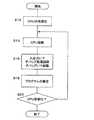
図3はデバッグ処理を行う際のプログラム処理装置の動作を示すものである。 FIG. 3 shows the operation of the program processing apparatus when performing the debugging process.
ステップS12では、CPU2の初期化の処理が行われる。このとき、これまでCPU2で行われていた信号処理は一切破棄され、プログラムメモリ118内のプログラムに基づいた信号処理を開始するための準備が行われる。 In step S12, the
ステップS14ではCPU2が起動し、プログラムメモリ118に格納されたプログラムに基づいてCPU2が所定の信号処理を行う。 In step S14, the
ステップS16では、CPU2が行う信号処理に応じて、入出力インタフェース4、デバッグ処理回路10、デバッグインタフェース12、及び図示しない信号処理回路が活性とされる。これによって、デバッグコンピュータ200のデバッグツール210が動作し、プログラムの開発者はデバッグコンピュータ200を用いてデバッグ処理回路10での処理結果を確認してプログラムの検証を行うことが可能となる。 In step S16, the input /
そして、ステップS18では、デバッグコンピュータ200において、改良や修正を行ったプログラムをデバッグインタフェース12を介してプログラムメモリ118書き込む。 In step S18, the
ステップS20では、CPU2について初期化の処理が必要か否かを判断する。初期化の処理は、プログラムを修正するプログラムをプログラムメモリ118に書き込んだ後、その修正したプログラムを再度実行して検証を行う際に行われる。初期化が不要な場合はデバッグを終了して、CPU2は所定の信号処理を行う。初期化が必要な場合は初期化処理を行ってステップS18のCPU2の起動処理に移る。 In step S20, it is determined whether initialization processing is necessary for CPU2. The initialization process is performed when a program for correcting a program is written in the
このように、本実施形態では、デバッグ処理の際に、CPU2がプログラムメモリ118内のプログラムを実行して、デバッグコンピュータ200内のメモリ230内の変更後のプログラムをプログラムメモリ118に書き込む。メモリ230は十分な容量を持っており、ここにプログラムメモリ118内のメモリを全部書き込むことも可能である。また、書き換え前のプログラムをそのまま保持しながら、書き換えたプログラムを別に持つことができる。従って、ブレークポイントなどデバッグ用にプログラムメモリ118内のプログラムを書き換え、デバッグを終了した後、ブレークポイントなどの設定前のプログラムに戻すことも容易である。また、一部の変更データを別に持つことで、その部分のみを変更することも容易である。 As described above, in the present embodiment, during the debugging process, the
特に、CPU2は、プログラムメモリ118内のプログラムを書き換える際には、そのプログラムをイレーズ単位(例えば、4kbyte)で書き換える。内部RAM8には、十分な領域がない。このため、デバッグツール210の指令によって、CPU2がプログラムを書き換える場合には、内部RAM8において使える容量に応じて、プログラムを書き換えプログラムメモリ118に書き込む必要があった。 In particular, when the
しかし、本実施形態では、書き換えたプログラムがメモリ230に用意される。CPU2は、多数回の書き込み命令を行うことなく、メモリ230からプログラムメモリ118内の該当アドレスに書き換え後のプログラムを転送する命令を実行すればよい。すなわち、プログラムメモリ118から読み出して実行するプログラム命令としては、1命令でメモリ230から読み出したプログラムのプログラムメモリ118への書き込みが行える。 However, in the present embodiment, the rewritten program is prepared in the
1 プログラム処理装置、2 CPU、4 入出力インタフェース、8 内部RAM、10 デバッグ処理回路、12 デバッグインタフェース、22 内部バス、118 プログラムメモリ、120 外部バス、200 デバッグコンピュータ、210 デバッグツール、220 デバッグ通信ライン、230 メモリ。 1 program processing device, 2 CPU, 4 input / output interface, 8 internal RAM, 10 debug processing circuit, 12 debug interface, 22 internal bus, 118 program memory, 120 external bus, 200 debug computer, 210 debug tool, 220
Claims (4)
Translated fromJapaneseこのプログラムメモリ内のプログラムを実行して各種処理を行うCPUと、プログラム実行における信号状態を検出するデバッグ処理回路を含むプログラム処理装置と、
このプログラム処理装置内のデバッグ処理回路にそのモニター条件のデータを供給するとともに、デバッグ処理回路からの検出した信号状態についてのデータを受け取り、プログラム実行時の信号状態をモニターするデバッグコンピュータと、
を含むプログラム処理システムであって、
前記デバッグコンピュータはメモリを備え、前記プログラムメモリに記憶されているプログラムを前記プログラムメモリのイレーズ単位で前記メモリに記憶し、これに所定の編集を加え、前記プログラム処理装置に供給し、前記プログラム処理装置がイレーズ単位の編集後のプログラムを前記プログラムメモリに書き込むことを特徴とするプログラム処理システム。A program memory that stores a program and erases stored data for each predetermined erase unit;
CPU for executing various processes by executing a program in the program memory, a program processing apparatus including a debug processing circuit for detecting a signal state in program execution,
A debug computer that supplies data on the monitoring conditions to the debug processing circuit in the program processing device, receives data on the detected signal state from the debug processing circuit, and monitors the signal state at the time of program execution;
A program processing system comprising:
The debug computer includes a memory, stores a program stored in the program memory in the memory in erase units of the program memory, performs predetermined editing on the program, supplies the program to the program processing device, and performs the program processing. A program processing system, wherein the apparatus writes an edited program in erase units into the program memory.
前記プログラムメモリは、フラッシュメモリであることを特徴とするプログラム処理システム。The program processing system according to claim 1,
The program processing system, wherein the program memory is a flash memory.
前記イレーズ単位の編集後プログラムの前記プログラムメモリへの書き込みは、前記プログラムメモリ内に記憶されている、1つの書き込み命令により実行されることを特徴とするプログラム処理システム。In the program processing system according to claim 1 or 2,
The program processing system according to claim 1, wherein writing of the post-edit program in the erase unit to the program memory is executed by a single write command stored in the program memory.
前記デバッグ処理回路は、外部に設けられたデバッグコンピュータからモニター条件のデータを得て、このモニター条件に基づきモニターを行い得られたモニターデータを前記デバッグコンピュータに供給し、前記デバッグコンピュータからプログラムの書き換え命令を受け取った場合には、前記プログラムメモリのイレーズ単位でプログラムを前記デバッグコンピュータに供給し、前記デバッグコンピュータにおいて書き換えられたイレーズ単位のプログラムを前記プログラムメモリに書き込むことを特徴とするプログラム処理装置。A program processing apparatus including a CPU for executing various processes by executing a program in a program memory provided outside, and a debug processing circuit for monitoring a program execution state,
The debug processing circuit obtains monitor condition data from an externally provided debug computer, supplies the monitor data obtained by monitoring based on the monitor condition to the debug computer, and rewrites a program from the debug computer When receiving an instruction, the program processing apparatus supplies a program to the debug computer in erase units of the program memory, and writes the program in erase units rewritten in the debug computer into the program memory.
Priority Applications (1)
| Application Number | Priority Date | Filing Date | Title |
|---|---|---|---|
| JP2007238691AJP2009070195A (en) | 2007-09-14 | 2007-09-14 | Program processing system and program processing apparatus |
Applications Claiming Priority (1)
| Application Number | Priority Date | Filing Date | Title |
|---|---|---|---|
| JP2007238691AJP2009070195A (en) | 2007-09-14 | 2007-09-14 | Program processing system and program processing apparatus |
Publications (1)
| Publication Number | Publication Date |
|---|---|
| JP2009070195Atrue JP2009070195A (en) | 2009-04-02 |
Family
ID=40606363
Family Applications (1)
| Application Number | Title | Priority Date | Filing Date |
|---|---|---|---|
| JP2007238691APendingJP2009070195A (en) | 2007-09-14 | 2007-09-14 | Program processing system and program processing apparatus |
Country Status (1)
| Country | Link |
|---|---|
| JP (1) | JP2009070195A (en) |
Cited By (1)
| Publication number | Priority date | Publication date | Assignee | Title |
|---|---|---|---|---|
| JP7532344B2 (en) | 2019-04-10 | 2024-08-13 | ローム株式会社 | Semiconductor device and debugging system |
- 2007
- 2007-09-14JPJP2007238691Apatent/JP2009070195A/enactivePending
Cited By (1)
| Publication number | Priority date | Publication date | Assignee | Title |
|---|---|---|---|---|
| JP7532344B2 (en) | 2019-04-10 | 2024-08-13 | ローム株式会社 | Semiconductor device and debugging system |
Similar Documents
| Publication | Publication Date | Title |
|---|---|---|
| US6798713B1 (en) | Implementing software breakpoints | |
| CN112947977A (en) | Software online upgrading method and system | |
| US7363544B2 (en) | Program debug method and apparatus | |
| JP2008009721A (en) | Evaluation system and evaluation method thereof | |
| JP2005071303A (en) | Program start device | |
| JP2005070949A (en) | Program processing apparatus | |
| US7574585B1 (en) | Implementing software breakpoints and debugger therefor | |
| JP2005070950A (en) | Program processing apparatus | |
| KR20060122064A (en) | Electronic device and its booting method | |
| JP2009070195A (en) | Program processing system and program processing apparatus | |
| US10642601B2 (en) | Apparatus and methods for in-application programming of flash-based programmable logic devices | |
| JP4976817B2 (en) | Program processing apparatus and program processing method | |
| US11521698B2 (en) | Testing read-only memory using memory built-in self-test controller | |
| JP2004021922A (en) | Memory pseudo fault injection device | |
| JP2009223435A (en) | Data storage method and device, and program | |
| TWI517166B (en) | Non-volatile memory apparatus | |
| JPH09305395A (en) | Electronic equipment | |
| JP2007213415A (en) | Memory device | |
| JP4324149B2 (en) | Emulator and development support system using it | |
| JP4543505B2 (en) | Microcomputer control method and abnormality monitoring device | |
| JP2011150383A (en) | Firmware writing method | |
| JP2001147863A (en) | Flash memory rewrite device | |
| JP2004013338A (en) | Data processor and method | |
| CN120723318A (en) | BIOS firmware adaptation method, device, electronic device and readable medium | |
| JP2023020590A (en) | Information processing device and monitoring method |