JP2009064847A - Nonvolatile memory transistor, nonvolatile memory device, and data erasing method of nonvolatile memory transistor - Google Patents
Nonvolatile memory transistor, nonvolatile memory device, and data erasing method of nonvolatile memory transistorDownload PDFInfo
- Publication number
- JP2009064847A JP2009064847AJP2007229673AJP2007229673AJP2009064847AJP 2009064847 AJP2009064847 AJP 2009064847AJP 2007229673 AJP2007229673 AJP 2007229673AJP 2007229673 AJP2007229673 AJP 2007229673AJP 2009064847 AJP2009064847 AJP 2009064847A
- Authority
- JP
- Japan
- Prior art keywords
- gate electrode
- source
- floating gate
- nonvolatile memory
- drain
- Prior art date
- Legal status (The legal status is an assumption and is not a legal conclusion. Google has not performed a legal analysis and makes no representation as to the accuracy of the status listed.)
- Pending
Links
- 230000015654memoryEffects0.000titleclaimsabstractdescription96
- 238000000034methodMethods0.000titleclaimsabstractdescription41
- 239000000758substrateSubstances0.000claimsabstractdescription64
- 239000004065semiconductorSubstances0.000claimsabstractdescription62
- 230000015556catabolic processEffects0.000claimsabstractdescription21
- 230000008878couplingEffects0.000claimsdescription19
- 238000010168coupling processMethods0.000claimsdescription19
- 238000005859coupling reactionMethods0.000claimsdescription19
- 230000015572biosynthetic processEffects0.000claimsdescription11
- 239000011159matrix materialSubstances0.000claimsdescription4
- 239000010410layerSubstances0.000description25
- 238000010586diagramMethods0.000description5
- 239000002784hot electronSubstances0.000description5
- 238000009792diffusion processMethods0.000description2
- 230000006870functionEffects0.000description2
- 239000002344surface layerSubstances0.000description2
- 239000012141concentrateSubstances0.000description1
- 239000012535impuritySubstances0.000description1
Images


Landscapes
- Non-Volatile Memory (AREA)
- Read Only Memory (AREA)
- Semiconductor Memories (AREA)
Abstract
Description
Translated fromJapanese本発明は、いわゆるスプリットゲート構造を有する不揮発性メモリトランジスタ、不揮発性メモリ装置および不揮発性メモリトランジスタのデータ消去方法に関するものである。 The present invention relates to a nonvolatile memory transistor having a so-called split gate structure, a nonvolatile memory device, and a data erasing method of the nonvolatile memory transistor.
スプリットゲート構造を有する不揮発性メモリ(不揮発性メモリトランジスタ)100は、例えば、図4に示すように、P型の半導体基板101と、この半導体基板101上に形成されるゲート酸化膜104と、このゲート酸化膜104上に形成される浮遊ゲート電極105と、この浮遊ゲート電極105の上部および側部に酸化膜106を介して形成され一部108aが半導体基板101のチャネル形成領域Ch上で浮遊ゲート電極105と並んで配置される制御ゲート電極108と、を備えている。そして、これに書き込まれたデータを消去する方法としては、例えば、下記特許文献1に開示される「不揮発性半導体記憶装置の消去方法」がある。 A nonvolatile memory (nonvolatile memory transistor) 100 having a split gate structure includes, for example, a P-
なお、図4に示す半導体基板101の表面には、n+拡散層からなるソース102とドレイン103とがそれぞれ形成されており、これらは半導体基板101よりも高い不純物濃度のP型領域(図略)でくるまれている。また、ゲート酸化膜104は、ソース−ドレイン間の半導体基板11の表面を覆う厚さ70Å〜200Åのトンネル膜として機能する。さらに、酸化膜106は、酸化膜−窒化膜−酸化膜の3層構造からなる。 Note that a
このように構成される不揮発性メモリ100のデータの書込みは、チャネルホットエレクトロン(CHE;Channel Hot Electron)またはドレインアバランシェチャネルホットエレクトロン(DACHE;Drain Avalanche Channel Hot Electron)と称される現象を用いて行われる。 Data writing in the
即ち、図4(A) に示すように、例えば、ドレイン103に5V(=Vd)を、制御ゲート電極108に8V(=Vcg)を、それぞれ印加し、ソース102および半導体基板11を接地(0V(=Vs,Vb))して、ドレイン103の近傍でのインパクトイオニゼーションにより生じた電子eを浮遊ゲート電極105に注入する。これにより、MOSトランジスタとしての不揮発性メモリ100の閾値電圧Vtが上がるので、データが書き込まれた状態となる。 That is, as shown in FIG. 4A, for example, 5 V (= Vd) is applied to the
これに対してデータの消去は、ホットホール(HH;Hot Hole)消去と称される方法で行われる。即ち、図4(B) に示すように、制御ゲート電極108および半導体基板101を接地(0V(=Vcg,Vb))し、ソース102を開放(Open(=Vs))した状態で、ドレイン103と半導体基板11との間でアバランシェブレークダウンが生じる電圧、例えば8V(=Vd)をドレイン103に印加する。これにより発生した高エネルギー状態にあるホール(ホットホール)を浮遊ゲート電極105に注入することによって、データの書込みで浮遊ゲート電極105に帯電した電子eが中和される。これにより、不揮発性メモリ100の閾値電圧Vtが下がるので、データが消去された状態になる。
しかしながら、このような従来の不揮発性メモリ100によると、上述したように、データの書込みおよび消去は、いずれもドレイン電圧Vdをドレイン103に印加する駆動制御を行っているため、不揮発性メモリ100のデータを書き換えるたびにドレイン103の近傍に位置するゲート酸化膜104にダメージが集中し易くなるという問題がある。 However, according to such a conventional
また、図5に示すように、不揮発性メモリ100をマトリックス状に配列するメモリセルアレー120を構成した場合には、データの書込みや消去にドレイン電圧Vdを印加する必要上、ビット線(ドレイン線D1〜D4)を使用することになるため、データを消去するときにもビット線単位でのまとまり、例えば、ビット線D1を選択したときには図5に示す一点鎖線内の不揮発性メモリ100をひとまとまりとして消去する。このため、一般的なEEPROMと同様にワード単位で消去する仕様要求に応えることができないという問題がある。 Further, as shown in FIG. 5, when the
本発明は、上述した課題を解決するためになされたものであり、その目的とするところは、ドレイン側のゲート酸化膜に与え得るダメージを軽減し得る不揮発性メモリトランジスタ、不揮発性メモリ装置および不揮発性メモリトランジスタのデータ消去方法を提供することにある。
また、本発明の別の目的は、メモリセルアレーを構成した場合には、ワード単位でまとめてデータを消去し得る不揮発性メモリトランジスタ、不揮発性メモリ装置および不揮発性メモリトランジスタのデータ消去方法を提供することにある。The present invention has been made to solve the above-described problems, and an object of the present invention is to provide a nonvolatile memory transistor, a nonvolatile memory device, and a nonvolatile memory that can reduce damage that can be caused to a gate oxide film on the drain side It is an object of the present invention to provide a data erasing method for a volatile memory transistor.
Another object of the present invention is to provide a non-volatile memory transistor, a non-volatile memory device, and a non-volatile memory transistor data erasing method capable of erasing data in units of words when a memory cell array is configured. There is to do.
上記目的を達成するため、特許請求の範囲に記載の請求項1の不揮発性メモリトランジスタでは、半導体基板と、この半導体基板上に形成されるゲート酸化膜と、このゲート酸化膜上に形成される浮遊ゲート電極と、この浮遊ゲート電極の上部および側部に酸化膜を介して形成され一部が前記半導体基板のチャネル形成領域上で前記浮遊ゲート電極と並んで配置される制御ゲート電極と、を備えた不揮発性メモリトランジスタであって、データの消去過程において、前記浮遊ゲート電極と並んで配置される前記制御ゲート電極の前記一部の下方でソースから前記浮遊ゲート電極のソース側端まで伸びる空乏層における前記浮遊ゲート電極のソース側端近傍と前記半導体基板との間でアバランシェブレークダウンが生じる電圧を前記ソースに印加することを技術的特徴とする。 In order to achieve the above object, in the nonvolatile memory transistor according to
特許請求の範囲に記載の請求項2の不揮発性メモリトランジスタでは、前記浮遊ゲート電極の上部には、前記浮遊ゲート電極の上部に形成される前記制御ゲート電極の残部に並んで、前記浮遊ゲート電極に対して容量結合可能な結合電極が形成される請求項1記載の不揮発性メモリトランジスタであって、前記データの消去過程において、前記結合電極には、前記制御ゲート電極、前記ソース、ドレインおよび前記半導体基板のいずれの電位よりも低い電圧が印加されることを技術的特徴とする。 The nonvolatile memory transistor according to claim 2, wherein the floating gate electrode is arranged above the floating gate electrode alongside a remaining portion of the control gate electrode formed on the floating gate electrode. 2. The nonvolatile memory transistor according to
特許請求の範囲に記載の請求項3の不揮発性メモリトランジスタでは、前記浮遊ゲート電極のドレイン側端が、前記ゲート酸化膜を介して前記ドレインと容量結合可能に前記ドレインに重なって位置する請求項1または2記載の不揮発性メモリトランジスタであって、データの消去過程において、前記ドレインには、前記ソースおよび前記制御ゲート電極の電位以下かつ前記半導体基板の電位以上の電圧が印加されることを技術的特徴とする。 3. The nonvolatile memory transistor according to claim 3, wherein a drain side end of the floating gate electrode is positioned to overlap the drain so as to be capacitively coupled to the drain through the gate oxide film. 3. The nonvolatile memory transistor according to
特許請求の範囲に記載の請求項4の不揮発性メモリトランジスタでは、請求項1〜3のいずれか一項に記載の不揮発性メモリトランジスタにおいて、データの消去過程において、前記制御ゲート電極には、前記ソースの電位よりも高い電圧が印加されることを技術的特徴とする。 In the nonvolatile memory transistor according to claim 4, the nonvolatile memory transistor according to any one of
上記目的を達成するため、特許請求の範囲に記載の請求項5の不揮発性メモリ装置では、請求項1〜4のいずれか一項に記載の不揮発性メモリトランジスタをマトリクス状に複数配置して構成される不揮発性メモリ装置であって、同一の行または列に配置される複数の前記不揮発性メモリトランジスタは、それぞれの前記ソースに接続されるソース電極が同一のソース配線に接続され、かつ、それぞれの前記制御ゲート電極が同一の制御ゲート配線に接続されることを技術的特徴とする。 In order to achieve the above object, the nonvolatile memory device according to claim 5 according to the claims includes a plurality of nonvolatile memory transistors according to any one of
上記目的を達成するため、特許請求の範囲に記載の請求項6の不揮発性メモリトランジスタのデータ消去方法では、半導体基板と、この半導体基板上に形成されるゲート酸化膜と、このゲート酸化膜上に形成される浮遊ゲート電極と、この浮遊ゲート電極の上部および側部に酸化膜を介して形成され一部が前記半導体基板のチャネル形成領域上で前記浮遊ゲート電極と並んで配置される制御ゲート電極と、を備えた不揮発性メモリトランジスタのデータ消去方法であって、前記浮遊ゲート電極と並んで配置される前記制御ゲート電極の前記一部の下方においてソースから前記浮遊ゲート電極のソース側端まで伸びる空乏層における前記浮遊ゲート電極のソース側端近傍と前記半導体基板との間でアバランシェブレークダウンが生じる電圧を前記ソースに印加することを技術的特徴とする。 In order to achieve the above object, in the data erasing method for a nonvolatile memory transistor according to claim 6, the semiconductor substrate, a gate oxide film formed on the semiconductor substrate, and the gate oxide film are formed. And a control gate which is formed on the upper and side portions of the floating gate electrode via an oxide film and a part thereof is arranged alongside the floating gate electrode on the channel formation region of the semiconductor substrate. A method for erasing data of a nonvolatile memory transistor comprising an electrode, from a source to a source side end of the floating gate electrode below the part of the control gate electrode arranged side by side with the floating gate electrode A voltage at which an avalanche breakdown occurs between the vicinity of the source side end of the floating gate electrode and the semiconductor substrate in the extending depletion layer And technical features that applied to the source.
特許請求の範囲に記載の請求項7の不揮発性メモリトランジスタのデータ消去方法では、前記浮遊ゲート電極のドレイン側端が、前記ゲート酸化膜を介して前記ドレインと容量結合可能に前記ドレインに重なって位置する請求項6記載の不揮発性メモリトランジスタのデータ消去方法であって、前記ドレインには、前記ソースおよび前記制御ゲート電極の電位以下かつ前記半導体基板の電位以上の電圧が印加されることを技術的特徴とする。 In the data erasing method of the nonvolatile memory transistor according to claim 7, the drain side end of the floating gate electrode overlaps the drain so as to be capacitively coupled to the drain via the gate oxide film. 7. The data erasing method for a non-volatile memory transistor according to claim 6, wherein a voltage lower than the potential of the source and the control gate electrode and higher than the potential of the semiconductor substrate is applied to the drain. Characteristic.
特許請求の範囲に記載の請求項8の不揮発性メモリトランジスタのデータ消去方法では、請求項6または7記載の不揮発性メモリトランジスタのデータ消去方法において、前記制御ゲート電極には、前記ソースの電位よりも高い電圧が印加されることを技術的特徴とする。 The data erasing method of the nonvolatile memory transistor according to
請求項1の発明や請求項6の発明では、データの消去過程において、浮遊ゲート電極と並んで配置される制御ゲート電極の一部の下方でソースから浮遊ゲート電極のソース側端まで伸びる空乏層における浮遊ゲート電極のソース側端近傍(空乏層の先端)と半導体基板との間でアバランシェブレークダウンが生じる電圧をソースに印加する。これにより、アバランシェブレークダウンにより発生した高エネルギー状態にあるホールを浮遊ゲート電極に注入し、データの書込みで浮遊ゲート電極に帯電した電子を中和することができる。 In the invention of
つまり、ドレインに電圧を印加することなく、ソースに電圧を印加することによりデータを消去し得るので、書込みをドレイン側から行っても消去はソース側から行うことが可能になる。したがって、書込みおよび消去をドレイン側から行う場合に比べて、ドレイン側のゲート酸化膜に与え得るダメージを軽減することができる。また、データの消去をソース側から行うことが可能になるので、メモリセルアレーを構成した場合にはワード単位でまとめてデータを消去することができる。 That is, since data can be erased by applying a voltage to the source without applying a voltage to the drain, erasing can be performed from the source side even if writing is performed from the drain side. Therefore, damage that can be caused to the gate oxide film on the drain side can be reduced as compared with the case where writing and erasing are performed from the drain side. Further, since data can be erased from the source side, when a memory cell array is configured, data can be erased collectively in units of words.
請求項2の発明では、データの消去過程において、浮遊ゲート電極に対して容量結合可能な結合電極には、制御ゲート電極、ソース、ドレインおよび半導体基板のいずれの電位よりも低い電圧が印加される。これにより、結合電極に容量的に結合する浮遊ゲート電極の電位を、結合電極の電位とほぼ同様に、制御ゲート電極、ソース、ドレインおよび半導体基板のいずれの電位よりも低い電圧に固定できるので、浮遊ゲートのソース側端の近傍のチャネルの電位をこのような低い電圧に下げられる。したがって、空乏層の浮遊ゲート電極のソース側端近傍(空乏層の先端)と半導体基板との間でアバランシェブレークダウンをより確実に生じさせることができる。また、浮遊ゲート電極の電位を結合電極の電位により制御できるため、これを用いてアバランシェブレークダウンが発生する電圧を調整することが可能となる。 In the data erasing process, a voltage lower than any potential of the control gate electrode, the source, the drain, and the semiconductor substrate is applied to the coupling electrode that can be capacitively coupled to the floating gate electrode. . As a result, the potential of the floating gate electrode capacitively coupled to the coupling electrode can be fixed to a voltage lower than any of the potential of the control gate electrode, the source, the drain, and the semiconductor substrate, almost the same as the potential of the coupling electrode. The potential of the channel near the source side end of the floating gate can be lowered to such a low voltage. Therefore, avalanche breakdown can be more reliably generated between the vicinity of the source side end of the floating gate electrode of the depletion layer (tip of the depletion layer) and the semiconductor substrate. In addition, since the potential of the floating gate electrode can be controlled by the potential of the coupling electrode, it is possible to adjust the voltage at which avalanche breakdown occurs using this.
請求項3の発明や請求項7の発明では、浮遊ゲート電極のドレイン側端が、ゲート酸化膜を介してドレインと容量結合可能にドレインに重なって位置し、ドレインには、ソースおよび制御ゲート電極の電位以下かつ半導体基板の電位以上の電圧が印加される。これにより、浮遊ゲート電極の電位を、ドレインの電位とほぼ同様に、ソースおよび制御ゲート電極の電位以下かつ半導体基板の電位以上に固定できるので、浮遊ゲートのソース側端の近傍のチャネルの電位をこのような電位に下げられる。したがって、空乏層の浮遊ゲートのソース側端近傍と半導体基板との間でアバランシェブレークダウンをより確実に生じさせることができる。また、浮遊ゲート電極の電位をドレインの電位により制御できるため、これを用いてアバランシェブレークダウンが発生する電圧を調整することが可能となる。 In the invention of claim 3 and claim 7, the drain side end of the floating gate electrode is positioned so as to be capacitively coupled with the drain via the gate oxide film, and the drain includes the source and the control gate electrode. A voltage equal to or lower than that of the semiconductor substrate and higher than that of the semiconductor substrate is applied. As a result, the potential of the floating gate electrode can be fixed to be equal to or lower than the potential of the source and control gate electrode and higher than the potential of the semiconductor substrate, almost the same as the potential of the drain. It is lowered to such a potential. Therefore, an avalanche breakdown can be more reliably generated between the vicinity of the source side end of the floating gate of the depletion layer and the semiconductor substrate. In addition, since the potential of the floating gate electrode can be controlled by the potential of the drain, it is possible to adjust the voltage at which avalanche breakdown occurs using this.
請求項4の発明や請求項8の発明では、制御ゲート電極には、ソースの電位よりも高い電圧が印加される。これにより、制御ゲート電極には、アバランシェ電圧よりも高い電圧が印加されるので、空乏層の浮遊ゲート電極のソース側端近傍と半導体基板との間におけるアバランシェブレークダウンの発生を促進することができる。したがって、アバランシェブレークダウンをより一層確実に生じさせることができる。 In the fourth and eighth aspects of the invention, a voltage higher than the source potential is applied to the control gate electrode. Thereby, since a voltage higher than the avalanche voltage is applied to the control gate electrode, it is possible to promote the occurrence of avalanche breakdown between the vicinity of the source side end of the floating gate electrode of the depletion layer and the semiconductor substrate. . Therefore, an avalanche breakdown can be generated more reliably.
請求項5の発明では、同一の行または列に配置される複数の不揮発性メモリトランジスタは、それぞれのソースに接続されるソース電極が同一のソース配線に接続され、かつ、それぞれの制御ゲート電極が同一の制御ゲート配線に接続される。これにより、これらの不揮発性メモリトランジスタに書き込まれたデータを消去する際には、各不揮発性メモリトランジスタに対して、ソース線単位、つまりワード単位でソース電圧を印加することができるので、同一の行または列に配置される複数の不揮発性メモリトランジスタのデータを同時に一括して消去することができる。したがって、ワード単位でまとめてデータを消去することができる。 According to the invention of claim 5, in the plurality of nonvolatile memory transistors arranged in the same row or column, the source electrodes connected to the respective sources are connected to the same source wiring, and the respective control gate electrodes are Connected to the same control gate wiring. Thus, when erasing data written in these nonvolatile memory transistors, the source voltage can be applied to each nonvolatile memory transistor in units of source lines, that is, in units of words. Data of a plurality of nonvolatile memory transistors arranged in a row or column can be erased simultaneously at the same time. Therefore, data can be erased collectively in units of words.
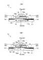
以下、本発明の「半導体記憶装置およびそのデータ消去方法」を適用した不揮発性メモリとそれに記憶されたデータの消去過程の実施形態について図を参照して説明する。まず本実施形態に係る不揮発性メモリ10の構成を図1に基づいて説明する。なお、図1は、不揮発性メモリ10の構成例およびその駆動例を示す説明図(図1(A) は書込み過程を示すもの、図1(B) は消去過程を示すもの)で、不揮発性メモリ10の断面を模式的に示したものである。 Embodiments of a nonvolatile memory to which the “semiconductor memory device and data erasing method thereof” of the present invention are applied and an erasing process of data stored in the nonvolatile memory will be described below with reference to the drawings. First, the configuration of the
図1(A) に示すように、不揮発性メモリ10は、スプリットゲート構造を有する半導体記憶装置で、いわゆるフラッシュメモリのメモリセル(Nチャネル型MOSトランジスタ)に相当するものである。 As shown in FIG. 1A, a
本実施形態では、例えば、P導電型の半導体基板(またはN導電型の半導体基板の表層部に形成されるP導電型のウェル)11内に対称に形成されるN導電型拡散領域(N+)のソース12およびドレイン13、これらに挟まれてチャネルとして機能し得るチャネル形成領域Ch、この半導体基板11の表層(半導体基板上)に形成されるゲート酸化膜14、このゲート酸化膜14(70Å〜200Åのトンネル膜)上に形成される浮遊ゲート電極15、制御ゲート電極18等から構成されている。 In the present embodiment, for example, an N conductivity type diffusion region (N +) formed symmetrically in a P conductivity type semiconductor substrate (or a P conductivity type well formed in a surface layer portion of an N conductivity type semiconductor substrate) 11.
浮遊ゲート電極15は、チャネル形成領域Ch上のゲート酸化膜14上のドレイン13側に片寄って図1の紙面垂直方向に帯状に形成されている。この浮遊ゲート電極15の周囲は、酸化膜16で覆われており、これを介して浮遊ゲート電極15の上部および側部に制御ゲート電極18が形成されている。なお、この酸化膜16は、例えば、酸化膜−窒化膜−酸化膜の三層構造のいわゆるONO膜で構成されている。 The floating
即ち、制御ゲート電極18は、その一部18aが酸化膜16を介して浮遊ゲート電極15上の一部を覆うように、またこの一部18aに連続して残部18bがソース12方向に位置する浮遊ゲート電極15の側部を覆いながらソース12側のゲート酸化膜14上に位置するように、それぞれ形成されている。これにより、制御ゲート電極18と浮遊ゲート電極15とがチャネル形成領域Ch上において並んで配置される、スプリットゲート構造をなしている。また、ドレイン13と浮遊ゲート電極15とがゲート酸化膜14を介してオーバラップする(重なる)ように配置されており、電気的に比較的大きな結合容量で容量結合可能に構成されている。 That is, the
なお、ドレイン13をP−層でくるむ場合にはポケット13aが形成される(図1に示すドレイン13先端下部の破線)。また、ソース12にはソース電圧Vs、ドレイン13にはドレインVd、制御ゲート電極18には制御ゲート電圧Vcg、をそれぞれ印加可能に配線されている。また半導体基板11にも基板電圧Vbを印加可能に配線されている。 When the
このように不揮発性メモリ10を構成することにより、例えば、データの書込み過程においては、図1(A) に示すような各電圧がソース12、ドレイン13、制御ゲート電極18および半導体基板11に印加される。 By configuring the
即ち、データの書込みにおいては、ソース電圧Vsおよび基板電圧Vbを同電位、例えば0Vにするため、ソース12および半導体基板11をそれぞれ接地し、基板電圧Vbに対して正の電圧(例えば5V)をドレイン電圧Vdとしてドレイン13に印加した状態で、基板電圧Vbに対して正の電圧(例えば8V)の制御ゲート電圧Vcgを制御ゲート電極18に印加する。 That is, in writing data, in order to set the source voltage Vs and the substrate voltage Vb to the same potential, for example, 0 V, the
不揮発性メモリ10を駆動する電圧関係をこのように設定することで、図1(A) に示す太矢印方向にソース12からドレイン13に向かって電子eが移動し、そのうちの一部の電子eが高エネルギー状態にあるホットエレクトロン(HE;Hot Electron)として、同図に細矢印で示すように浮遊ゲート電極15に注入される。これにより、MOSトランジスタとしての不揮発性メモリ10の閾値電圧Vtが上昇するため、例えばこれをデータが書き込まれた状態と定義することで、データの書込みとなる。 By setting the voltage relationship for driving the
これに対し、データの消去過程においては、図1(B) に示すような各電圧がソース12、ドレイン13、制御ゲート電極18および半導体基板11に印加される。 On the other hand, in the data erasing process, voltages as shown in FIG. 1B are applied to the
即ち、データの消去においては、ドレイン電圧Vdを例えば0Vにするためドレイン13を接地した状態で、ドレイン電圧Vdに対して正の電圧(例えば8V)を制御ゲート電圧Vcgとして制御ゲート電極18に印加する。これにより、ソース−ドレイン間のチャネル形成領域Chにチャネルが形成されるので、そのうえでドレイン電圧Vdに対して正の電圧(例えば8V)のソース電圧Vsをソース12に印加し、半導体基板11には例えば0Vを印加する。これにより、ゲート酸化膜14上に配置された制御ゲート電極18の一部18aの下にあたるチャネル形成領域Chでは空乏層Dpが形成されてドレイン13方向および半導体基板11の高電位方向に伸びる。 That is, in erasing data, a positive voltage (for example, 8 V) with respect to the drain voltage Vd is applied to the
このとき、浮遊ゲート電極15は、ドレインに対して電気的に容量結合可能にオーバラップしているので、浮遊ゲート電極15の電位はドレインの電位(0V)よりも低い電位に保たれる。つまり、浮遊ゲート電極15が結合容量を介して実質的に接地されるため、浮遊ゲート電極15の電位は0Vになる。 At this time, since the floating
このため、空乏層Dpの成長を浮遊ゲート電極15の下で止めるとともに、空乏層Dpの伸展方向先端付近、つまり空乏層の浮遊ゲート電極15のソース側端15aの近傍付近(空乏層先端Dppと半導体基板11との間)αでアバランシェブレークダウンが生じる。このため、アバランシェブレークダウンにより発生した高エネルギー状態にあるホールh、つまりホットホール(HH;Hot Hole)hが浮遊ゲート電極15に注入されると、データの書込みで浮遊ゲート電極15に帯電した電子eが中和されることから、MOSトランジスタとしての不揮発性メモリ10の閾値電圧Vtが降下して書き込まれたデータは消去(ホットホール消去)される。 For this reason, the growth of the depletion layer Dp is stopped under the floating
特に、ソース12に印加されるソース電圧Vsよりも高い電圧を制御ゲート電極18に印加することにより、チャネルChが形成され易くなるため、浮遊ゲート電極15のソース側端の近傍(空乏層先端Dppと半導体基板11との間)αでアバランシェブレークダウンをより確実に生じさせることができる。 In particular, since a channel Ch is easily formed by applying a voltage higher than the source voltage Vs applied to the
このように本実施形態に係る不揮発性メモリ10によると、データの消去過程において、浮遊ゲート電極15と並んで配置される制御ゲート電極18の一部18aの下方でソース12から浮遊ゲート電極15のソース側端15aまで伸びる空乏層Dpにおける浮遊ゲート電極15のソース側端15a近傍(空乏層先端Dpp)と半導体基板11との間αでアバランシェブレークダウンが生じる電圧をソース12に印加する。これにより、アバランシェブレークダウンにより発生したホットホールhを浮遊ゲート電極15に注入することで、データの書込みで浮遊ゲート電極15に帯電した電子eを中和することができる。 As described above, according to the
つまり、ドレイン13にドレイン電圧Vdを印加することなく、ソース12にソース電圧Vsを印加することによりデータを消去し得るので、書込に過程でデータの書込みをドレイン13側から行ってもデータの消去はソース12側から行うことが可能になる。したがって、書込みおよび消去をドレイン13側から行う場合に比べて、ドレイン13側のゲート酸化膜14に与え得るダメージを軽減することができる。 In other words, since the data can be erased by applying the source voltage Vs to the
また、ドレイン13をP−層のポケット13aでくるむ構成を採る場合には、書き込み時のチャネルホットエレクトロン(CHE)の生成のみを考慮して構成すれば良いため、当該不揮発性メモリ10の設計を容易にすることが可能となる。 Further, when the
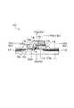
また、このように不揮発性メモリ10は、ソース12側からデータを消去することができることから、例えば、図2に示すように、不揮発性メモリ10をマトリックス状に配列してメモリセルアレー(不揮発性メモリ装置)を構成しても、複数の不揮発性メモリ10をワード単位でまとめてデータの消去をすることが可能となる。 Since the
即ち、図2に示すように、16個の不揮発性メモリ10を4行4列に配置し(図2に示す符号MC11,MC12,MC13,MC14,MC21,MC22,MC23,MC24,MC31,MC32,MC33,MC34,MC41,MC42,MC43,MC44)、隣り合う不揮発性メモリ10の、ドレイン13を行(図2に示す左右方向)に、ソース12および制御ゲート電極18を列(図2に示す上下方向)に、それぞれまとめて接続する。 That is, as shown in FIG. 2, 16
これにより、例えば、1行目に配置されるMC11,MC12,MC13,MC14のそれぞれのドレイン13にはドレイン線D1を介してドレイン電圧Vdを印加することができ、また1列目に配置されるMC11,MC21,MC31,MC41のそれぞれのソース12にはソース線S1を介してソース電圧Vsを印加することができ、さらに1列目に配置されるMC11,MC21,MC31,MC41のそれぞれの制御ゲート電極18には制御ゲート線CG1を介して制御ゲート電圧Vcgを印加することができる。なお、ソース線S1〜S4はソース配線、制御ゲート線CG1〜CG4は制御ゲート線に、それぞれ相当する。 Thereby, for example, the drain voltage Vd can be applied to each drain 13 of MC11, MC12, MC13, and MC14 arranged in the first row via the drain line D1, and arranged in the first column. A source voltage Vs can be applied to each
このため、図5を参照して説明した従来のメモリセルアレー120では、不揮発性メモリ100のデータを消去する際に、ビット線(ドレイン線D1〜D4)単位でのまとまりとして消去する必要があったが、図2に示すメモリセルアレー20では、不揮発性メモリ10のソース12にはソース線S1を介してワード線(ソース線S1〜S4)単位でソース電圧Vsを印加することができる。したがって、同図に示す一点鎖線内の不揮発性メモリ10のデータをワード単位でまとめて消去することができるので、一般的なEEPROMと同様、ワード単位で消去する仕様要求に応えることが可能となる。 For this reason, in the conventional
なお、図2に示すメモリセルアレー20では、不揮発性メモリ10を4行4列に配置したものを例示したが、実際には、このようなメモリセルアレーは、例えば100万個オーダーの不揮発性メモリ10で構成され、この場合においてもワード単位でまとめてデータを消去することができる。 In the
また、メモリセルアレー20は、ビット線(ドレイン線D1〜D4)およびソース線S1〜S4に接続される列選択回路と、ワード線(制御ゲート線CG1〜CG4)に接続される行選択回路と、これら選択回路に接続されてデータの書込み時、消去時および読出し時のそれぞれに、ドレイン電圧Vd、ソース電圧Vs、制御ゲート電圧Vcgおよび基板電圧Vbを制御し得る制御回路と、からなる駆動制御回路によって駆動制御される。 The
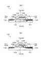
また、図3に示す不揮発性メモリ10’のように、制御ゲート電極18の残部18bに並んで、浮遊ゲート電極15に対して容量結合可能な結合電極19を酸化膜16を介して浮遊ゲート電極15の上部に形成し、データの消去過程において、制御ゲート電極18、ソース12、ドレイン13および半導体基板11のいずれの電位よりも低い電圧(例えば−8V)を結合電極19の結合電極電圧Vcpとして印加しても良い。 Further, as in the
これにより、結合電極19に容量的に結合する浮遊ゲート電極15の電位を、結合電極19の電位とほぼ同様に、制御ゲート電極18、ソース12、ドレイン13および半導体基板11のいずれの電位よりも低い結合電極電圧Vcp(例えば−8V)に固定できるので、浮遊ゲート電極15のソース側端15aの近傍のチャネル電位をこのような低い電圧に下げられる。したがって、浮遊ゲート電極15のソース側端15aの近傍でアバランシェブレークダウンをより確実に生じさせることができる。 As a result, the potential of the floating
また、この場合、結合電極電圧Vcpによって、アバランシェブレークダウンが発生する電圧を調整することが可能となる。さらに、ドレイン13と浮遊ゲート電極15とを電気的に容量結合可能にオーバラップさせる構成を採る必要もなくなるうえに、データの消去時にはドレイン電圧Vdを0Vに固定することなく開放電圧(電気的に浮かせた状態の電圧)に設定できるので、ラッチアップの発生も防止することができる。 In this case, the voltage at which avalanche breakdown occurs can be adjusted by the coupling electrode voltage Vcp. Further, it is not necessary to adopt a configuration in which the
10…不揮発性メモリ(不揮発性メモリトランジスタ)
11…半導体基板
12…ソース
13…ドレイン
13a…ポケット
14…ゲート酸化膜
15…浮遊ゲート電極
15a…浮遊ゲート電極のソース側端
16…酸化膜
18…制御ゲート電極
18a…制御ゲート電極の一部
18b…制御ゲート電極の残部
19…結合電極
20…メモリセルアレー(不揮発性メモリ装置)
e…電子
h…ホール
Ch…チャネル形成領域
CG1〜CG4…制御ゲート線(制御ゲート配線)
Dp…空乏層
Dpp…空乏層先端
MC11〜MC44…メモリセル(不揮発性メモリトランジスタ)
S1〜S4…ソース線(ソース配線)
α…空乏層先端と半導体基板との間(空乏層における浮遊ゲート電極のソース側端近傍と半導体基板との間)10: Non-volatile memory (non-volatile memory transistor)
DESCRIPTION OF
e ... electrons h ... holes Ch ... channel formation regions CG1 to CG4 ... control gate lines (control gate lines)
Dp ... depletion layer Dpp ... depletion layer tip MC11 to MC44 ... memory cell (nonvolatile memory transistor)
S1 to S4 ... Source line (source wiring)
α: Between the front end of the depletion layer and the semiconductor substrate (between the vicinity of the source side end of the floating gate electrode in the depletion layer and the semiconductor substrate)
Claims (8)
Translated fromJapaneseデータの消去過程において、前記浮遊ゲート電極と並んで配置される前記制御ゲート電極の前記一部の下方でソースから前記浮遊ゲート電極のソース側端まで伸びる空乏層における前記浮遊ゲート電極のソース側端近傍と前記半導体基板との間でアバランシェブレークダウンが生じる電圧を前記ソースに印加することを特徴とする不揮発性メモリトランジスタ。A semiconductor substrate, a gate oxide film formed on the semiconductor substrate, a floating gate electrode formed on the gate oxide film, and a part of the floating gate electrode formed on the upper and side portions via an oxide film Is a non-volatile memory transistor comprising a control gate electrode arranged alongside the floating gate electrode on a channel formation region of the semiconductor substrate,
In the data erasing process, the source side end of the floating gate electrode in the depletion layer extending from the source to the source side end of the floating gate electrode below the part of the control gate electrode arranged side by side with the floating gate electrode A non-volatile memory transistor, wherein a voltage causing an avalanche breakdown between a vicinity and the semiconductor substrate is applied to the source.
前記データの消去過程において、前記結合電極には、前記制御ゲート電極、前記ソース、ドレインおよび前記半導体基板のいずれの電位よりも低い電圧が印加されることを特徴とする不揮発性メモリトランジスタ。The coupling electrode capable of being capacitively coupled to the floating gate electrode is formed on the floating gate electrode alongside the remaining portion of the control gate electrode formed on the floating gate electrode. A non-volatile memory transistor,
The nonvolatile memory transistor, wherein a voltage lower than any potential of the control gate electrode, the source, the drain, and the semiconductor substrate is applied to the coupling electrode in the data erasing process.
データの消去過程において、前記ドレインには、前記ソースおよび前記制御ゲート電極の電位以下かつ前記半導体基板の電位以上の電圧が印加されることを特徴とする不揮発性メモリトランジスタ。3. The nonvolatile memory transistor according to claim 1, wherein a drain side end of the floating gate electrode is positioned to overlap the drain so as to be capacitively coupled to the drain through the gate oxide film,
In the data erasing process, a voltage lower than the potential of the source and the control gate electrode and higher than the potential of the semiconductor substrate is applied to the drain.
同一の行または列に配置される複数の前記不揮発性メモリトランジスタは、それぞれの前記ソースに接続されるソース電極が同一のソース配線に接続され、かつ、それぞれの前記制御ゲート電極が同一の制御ゲート配線に接続されることを特徴とする不揮発性メモリ装置。A non-volatile memory device configured by arranging a plurality of non-volatile memory transistors according to claim 1 in a matrix,
In the plurality of nonvolatile memory transistors arranged in the same row or column, the source electrodes connected to the sources are connected to the same source wiring, and the control gate electrodes are the same control gate. A non-volatile memory device connected to wiring.
前記浮遊ゲート電極と並んで配置される前記制御ゲート電極の前記一部の下方においてソースから前記浮遊ゲート電極のソース側端まで伸びる空乏層における前記浮遊ゲート電極のソース側端近傍と前記半導体基板との間でアバランシェブレークダウンが生じる電圧を前記ソースに印加することを特徴とする不揮発性メモリトランジスタのデータ消去方法。A semiconductor substrate, a gate oxide film formed on the semiconductor substrate, a floating gate electrode formed on the gate oxide film, and a part of the floating gate electrode formed on the upper and side portions via an oxide film Is a data erasing method of a nonvolatile memory transistor, comprising: a control gate electrode arranged alongside the floating gate electrode on a channel formation region of the semiconductor substrate,
Near the source side end of the floating gate electrode in the depletion layer extending from the source to the source side end of the floating gate electrode below the part of the control gate electrode arranged side by side with the floating gate electrode, and the semiconductor substrate A method for erasing data in a nonvolatile memory transistor, wherein a voltage causing an avalanche breakdown is applied to the source.
前記ドレインには、前記ソースおよび前記制御ゲート電極の電位以下かつ前記半導体基板の電位以上の電圧が印加されることを特徴とする不揮発性メモリトランジスタのデータ消去方法。The nonvolatile memory transistor data erasing method according to claim 6, wherein a drain side end of the floating gate electrode is positioned to overlap the drain so as to be capacitively coupled to the drain through the gate oxide film.
A data erasing method for a nonvolatile memory transistor, wherein a voltage lower than the potential of the source and the control gate electrode and higher than a potential of the semiconductor substrate is applied to the drain.
Priority Applications (1)
| Application Number | Priority Date | Filing Date | Title |
|---|---|---|---|
| JP2007229673AJP2009064847A (en) | 2007-09-05 | 2007-09-05 | Nonvolatile memory transistor, nonvolatile memory device, and data erasing method of nonvolatile memory transistor |
Applications Claiming Priority (1)
| Application Number | Priority Date | Filing Date | Title |
|---|---|---|---|
| JP2007229673AJP2009064847A (en) | 2007-09-05 | 2007-09-05 | Nonvolatile memory transistor, nonvolatile memory device, and data erasing method of nonvolatile memory transistor |
Publications (1)
| Publication Number | Publication Date |
|---|---|
| JP2009064847Atrue JP2009064847A (en) | 2009-03-26 |
Family
ID=40559203
Family Applications (1)
| Application Number | Title | Priority Date | Filing Date |
|---|---|---|---|
| JP2007229673APendingJP2009064847A (en) | 2007-09-05 | 2007-09-05 | Nonvolatile memory transistor, nonvolatile memory device, and data erasing method of nonvolatile memory transistor |
Country Status (1)
| Country | Link |
|---|---|
| JP (1) | JP2009064847A (en) |
- 2007
- 2007-09-05JPJP2007229673Apatent/JP2009064847A/enactivePending
Similar Documents
| Publication | Publication Date | Title |
|---|---|---|
| KR101274207B1 (en) | Method of operating non-volatile memory devices | |
| KR100454117B1 (en) | Methods of operating a non-volatile memory device having a silicon-oxide-nitride-oxide-silicon (SONOS) gate structure | |
| US8045386B2 (en) | Methods and apparatus for programming a memory cell using one or more blocking memory cells | |
| CN102568584B (en) | Integrated circuit including non-volatile memory cells with reduced punch-through leakage | |
| US7903465B2 (en) | Memory array of floating gate-based non-volatile memory cells | |
| CN101640067B (en) | Memory cell and array operation method for reducing punch-through leakage | |
| KR101489885B1 (en) | Charge Trap Nonvolatile Memory Device With Enhanced Reliability And Method Of Operating The Same | |
| JP4859292B2 (en) | Semiconductor integrated circuit device and NAND nonvolatile semiconductor device | |
| CN1391231A (en) | Program method for nonvolatile semiconductor memory | |
| JP5305856B2 (en) | Nonvolatile semiconductor memory | |
| US6822910B2 (en) | Non-volatile memory and operating method thereof | |
| JP5853853B2 (en) | Semiconductor memory device and driving method thereof | |
| JP2018190477A (en) | Nonvolatile semiconductor memory device | |
| JP5483826B2 (en) | Nonvolatile semiconductor memory device and writing method thereof | |
| KR20010072189A (en) | Semiconductor device with a non-volatile memory | |
| JP2009064847A (en) | Nonvolatile memory transistor, nonvolatile memory device, and data erasing method of nonvolatile memory transistor | |
| JPS6045067A (en) | Nonvolatile semiconductor memory device | |
| JP2007027369A (en) | Control method of non-volatile storage element | |
| JP5629968B2 (en) | Nonvolatile semiconductor memory cell and nonvolatile semiconductor memory device | |
| JP3420132B2 (en) | Nonvolatile semiconductor memory device | |
| KR20060070724A (en) | Programming method of flash memory device | |
| CN120529588A (en) | NOR type memory array, NOR type memory, and electronic device | |
| KR20080111963A (en) | Nonvolatile Memory Device and Formation Method | |
| KR20090069951A (en) | Nonvolatile Memory Devices | |
| JP2009158513A (en) | Nonvolatile semiconductor storage element, nonvolatile semiconductor storage device, data writing method of nonvolatile semiconductor storage element, and data rewriting method of nonvolatile semiconductor storage device |