JP2009054938A - Receiver module - Google Patents
Receiver moduleDownload PDFInfo
- Publication number
- JP2009054938A JP2009054938AJP2007222580AJP2007222580AJP2009054938AJP 2009054938 AJP2009054938 AJP 2009054938AJP 2007222580 AJP2007222580 AJP 2007222580AJP 2007222580 AJP2007222580 AJP 2007222580AJP 2009054938 AJP2009054938 AJP 2009054938A
- Authority
- JP
- Japan
- Prior art keywords
- light receiving
- receiving element
- wiring board
- base wiring
- light
- Prior art date
- Legal status (The legal status is an assumption and is not a legal conclusion. Google has not performed a legal analysis and makes no representation as to the accuracy of the status listed.)
- Pending
Links
- 239000000758substrateSubstances0.000claimsabstractdescription33
- 239000013307optical fiberSubstances0.000claimsabstractdescription14
- 239000000463materialSubstances0.000claimsdescription18
- 239000011347resinSubstances0.000claimsdescription15
- 229920005989resinPolymers0.000claimsdescription15
- 238000007789sealingMethods0.000claimsdescription14
- 230000004308accommodationEffects0.000claimsdescription7
- 230000002411adverseEffects0.000abstractdescription2
- 230000000694effectsEffects0.000abstractdescription2
- 230000003071parasitic effectEffects0.000abstractdescription2
- 239000004020conductorSubstances0.000description12
- 230000003287optical effectEffects0.000description9
- 239000000853adhesiveSubstances0.000description6
- 230000001070adhesive effectEffects0.000description6
- 238000004891communicationMethods0.000description5
- 238000010586diagramMethods0.000description5
- 229910000679solderInorganic materials0.000description5
- 238000003780insertionMethods0.000description4
- 230000037431insertionEffects0.000description4
- 239000000919ceramicSubstances0.000description2
- 230000006866deteriorationEffects0.000description2
- 238000007667floatingMethods0.000description2
- 239000011810insulating materialSubstances0.000description2
- 239000011159matrix materialSubstances0.000description2
- 238000000034methodMethods0.000description2
- VYPSYNLAJGMNEJ-UHFFFAOYSA-NSilicium dioxideChemical compoundO=[Si]=OVYPSYNLAJGMNEJ-UHFFFAOYSA-N0.000description1
- 230000003321amplificationEffects0.000description1
- 230000005540biological transmissionEffects0.000description1
- 230000008878couplingEffects0.000description1
- 238000010168coupling processMethods0.000description1
- 238000005859coupling reactionMethods0.000description1
- 239000011521glassSubstances0.000description1
- 238000004519manufacturing processMethods0.000description1
- 239000002184metalSubstances0.000description1
- 239000012299nitrogen atmosphereSubstances0.000description1
- 238000003199nucleic acid amplification methodMethods0.000description1
- 230000000149penetrating effectEffects0.000description1
- 230000002093peripheral effectEffects0.000description1
- 238000007747platingMethods0.000description1
- 238000007639printingMethods0.000description1
- 239000004065semiconductorSubstances0.000description1
- 230000035945sensitivityEffects0.000description1
- 238000007740vapor depositionMethods0.000description1
Images


Landscapes
- Light Receiving Elements (AREA)
Abstract
Translated fromJapaneseDescription
Translated fromJapanese本発明は、光ファイバ通信に用いられる受光モジュールに関する。 The present invention relates to a light receiving module used for optical fiber communication.
高速光ファイバ通信では、高速応答性と高い受光感度を有する受光素子が求められている。特に高速応答性を実現するためには、受光素子をフリップチップ実装することで、ボンディングワイヤによるインダクタンス成分、発生磁界の伝播などを低減する構造が提案されている。また、光ファイバ通信の高速化対応を満たす一方で、小型化、低コスト化も重要となっている。 In high-speed optical fiber communication, a light receiving element having high-speed response and high light receiving sensitivity is required. In particular, in order to realize high-speed response, a structure has been proposed in which the light receiving element is flip-chip mounted to reduce the inductance component due to the bonding wire, the propagation of the generated magnetic field, and the like. In addition, while satisfying the high-speed response of optical fiber communication, downsizing and cost reduction are also important.
これらの要求に対して、例えば、特許文献1には、配線膜と透光性樹脂膜を有する基板上に光素子をフリップチップ実装することで、小型化や高周波特性の改善を図ると共に、トランスファモールドにより気密封止して保護された構造の光通信モジュールが開示されている。また、特許文献2では、フリップチップ実装するに適した構造の受光素子が開示されている。さらに、特許文献3には、受光素子、発光素子を回路チップ上にフリップチップ実装することが開示されている。
特許文献1に開示の光通信モジュールは、複数の光素子をアライメント調整でフリップチップ実装し、この後、ダイシングにより各モジュールに分割している。しかし、その構造上、封止のためのトランスファモールドが必要とされが、個別のモジュールごとのモールドで行われているため量産性が悪い。量産性を高めるには、複数のモジュールを一度にトランスファモールドする必要があるが、これには、金型が大型になり設備投資の負担が大きくなる。
また、特許文献3に開示のように、回路チップ上に受光素子または発光素子をフリップチップ接続で実装することで信号の高速応答は期待できる。しかし、回路チップと配線基板間は、ワイヤ接続を行う構造であり改善の余地がある。In the optical communication module disclosed in
Further, as disclosed in
本発明は、上述した実情に鑑みてなされたもので、寄生インピーダンスによる高周波信号、高速応答への悪影響を抑制し、トランスファモールドを必要としない生産性のよい受光モジュールの提供を目的とする。 The present invention has been made in view of the above-described circumstances, and an object of the present invention is to provide a high-productivity light-receiving module that suppresses adverse effects on high-frequency signals and high-speed responses due to parasitic impedance and does not require a transfer mold.
本発明による受光モジュールは、受光素子がフリップチップ実装されたプリアンプ回路チップと、受光素子を収容する収容凹部を有し所定の光波長に対して透光性のあるベース配線基板と、光ファイバを接続保持するスリーブとを備える。前記のプリアンプ回路チップはベース配線基板にフリップチップ実装で搭載され、前記のスリーブは光ファイバからの信号光を受光素子で受光するように調芯されてベース配線基板に接着固定される。 A light-receiving module according to the present invention includes a preamplifier circuit chip on which a light-receiving element is flip-chip mounted, a base wiring board having a housing recess for housing the light-receiving element, and translucent to a predetermined light wavelength, and an optical fiber And a sleeve for holding the connection. The preamplifier circuit chip is mounted on the base wiring board by flip chip mounting, and the sleeve is aligned and fixed to the base wiring board so that signal light from the optical fiber is received by the light receiving element.
また、本発明による受光モジュールは、前記の受光素子が、入光面側に集光レンズを備える構成とされる。また、ベース配線基板上には、プリアンプ回路チップが収容される収容空間を有し、ベース配線基板の配線電極に電気接続された側面電極をもつカバー基板を備える構成とすることができる。さらに、前記のカバー基板の収容空間に封止樹脂材を充填して封止された構造とすることもできる。 In the light receiving module according to the present invention, the light receiving element includes a condensing lens on the light incident surface side. Further, the base wiring board may include a cover board having a storage space for storing the preamplifier circuit chip and having side electrodes electrically connected to the wiring electrodes of the base wiring board. Further, the housing space of the cover substrate may be filled with a sealing resin material and sealed.
本発明によれば、受光素子の接続電極面、プリアンプ回路チップの接続電極面およびベース配線基板の配線面を同一面に対向する形態で構成することができるので、これらの部品間の電気接続は全てフリップチップ実装が可能となる。この結果、ワイヤ接続による電気接続を省略することができ、浮遊インピーダンスによる高周波応答性の低下を抑制することができ、高周波特性に優れた受光モジュールを実現できる。
また、トランスファモールドを必要としない構造であるため金型の使用が不要で、大きなサイズのベース配線基板を用いてマトリックス状に組立てることが可能で、安価で生産性のよい受光モジュールを提供することが可能となる。According to the present invention, the connection electrode surface of the light receiving element, the connection electrode surface of the preamplifier circuit chip, and the wiring surface of the base wiring board can be configured to face the same surface. All flip chip mounting is possible. As a result, electrical connection by wire connection can be omitted, a decrease in high frequency response due to floating impedance can be suppressed, and a light receiving module having excellent high frequency characteristics can be realized.
In addition, since the structure does not require a transfer mold, there is no need to use a mold, and it is possible to assemble in a matrix using a large-sized base wiring board, and to provide a light receiving module that is inexpensive and has high productivity. Is possible.
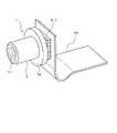
図により本発明の実施の形態を説明する。図1(A)は本発明による受光モジュールの概略を説明する斜視図、図1(B)はその断面図である。図中、1は受光モジュール、2は受光素子、3はプリアンプ回路チップ、4はベース配線基板、4aは収容凹部、5はカバー基板、5aは収容空間、6は封止樹脂材、7はスリーブ、7aはフランジ部、7bは挿着孔を示す。 Embodiments of the present invention will be described with reference to the drawings. FIG. 1A is a perspective view for explaining the outline of a light receiving module according to the present invention, and FIG. 1B is a sectional view thereof. In the figure, 1 is a light receiving module, 2 is a light receiving element, 3 is a preamplifier circuit chip, 4 is a base wiring board, 4a is a receiving recess, 5 is a cover substrate, 5a is a receiving space, 6 is a sealing resin material, and 7 is a sleeve. 7a is a flange portion, and 7b is an insertion hole.
本発明による受光モジュール1は、フォトダイオード(PD)等の受光素子2が実装されたプリアンプ回路チップ3と、該プリアンプ回路チップ3が実装搭載されるベース配線基板4と、ベース配線基板4に接着等により固定されるスリーブ7で構成される。プリアンプ回路チップ3は、受光素子2で受光した光電流をプリアンプ回路で電圧信号に変換される。このプリアンプ回路には、低雑音で広いダインミックレンジのものが要求されていて、通常は、増幅器の入力部と出力部の間に帰還抵抗を入れたトランスインピーダンス型のプリアンプ(TIA)が用いられる。このTIA回路は、プリアンプ回路チップ3として、一体化された矩形状のチップ状部品で提供される。 A
受光素子2は、後述するように、プリアンプ回路チップ3にフリップチップ実装が可能な形状のものが用いられ、プリアンプ回路チップ3の中央部分に電気的、機械的に接続される。ベース配線基板4は、受光素子2を収容する収容凹部4aを有し、所定の光波長に対して透光性のある絶縁材料が用いられ、収容凹部4aを設けた表面側に配線導体が形成されている。このベース配線基板4には、受光素子2を搭載したプリアンプ回路チップ3がフリップチップ実装で搭載される。 As will be described later, the
また、ベース配線基板4には、カバー基板5を接合して受光素子2およびプリアンプ回路チップ3を保護するようにすることができる。このカバー基板5にはプリアンプ回路チップ3が収容される収容空間5aを有し、必要に応じて、収容空間5a内に封止樹脂材6を充填して気密封止することができる。なお、封止樹脂材6が所定の光波長に対して透光性を有している場合は、ベース配線基板4の収容凹部4aにも充填させることができる。 Further, a
スリーブ7は、光ファイバを接続するための光コネクタを嵌合保持するためのもので、フランジ部7aでベース配線基板4に接着材等により固定される。このスリーブ7の挿着孔7bには、光ファイバの端部に取り付けられた光コネクタのフェルール(図示せず)が挿着され、外部装置からの信号光が受光素子2に向けて出射される。光ファイバから出射される信号光が、効率よく受光素子2で受光できるように、ベース配線基板4との接着に際しては調芯して位置決めされる。 The
図2は、受光素子2とプリアンプ回路チップ3の概略を説明する図である。受光素子2は、図2(A)に示すようなフリップチップ実装が可能な形状のもの(例えば、特許文献2に開示のような受光素子)が用いられる。この受光素子2は、中央部に受光部10を有し、この受光部10が接する実装面2a側において、電極リード11a,11bの端部に半田バンプ12が、蒸着法、めっき法、または印刷法等により形成されている。また、受光部10に対向する信号光が入射される入光面2b側には、集光レンズとしてモノシリックレンズ13が形成されていて、このレンズ13の光軸上にある光ファイバからの信号光を受光部13に集光させる。 FIG. 2 is a diagram for explaining the outline of the light receiving
プリアンプ回路チップ3は、例えば、トランスインピーダンス型のプリアンプ(TIA)で形成され(回路構成は省略)、実装面3aの中央部に上記した受光素子2をフリップチップ接続で直接実装させるための電極14が形成されている。また、プリアンプ回路チップ3の実装面3aには、この他、ベース配線基板4を介して次段の増幅回路等への接続のための接続電極15が設けられている。この接続電極15は、プリアンプ回路チップ3をベース配線基板4にフリップチップ接続で搭載するために、半田バンプで形成される。 The
図3は、受光素子2をフリップチップ実装したプリアンプ回路チップ3を、ベース配線基板4上にフリップチップ接続で実装する例を説明する図である。図2(B)で説明したように、プリアンプ回路チップ3には、受光素子2がプリアンプ回路チップ3の実装面3aから突出する形態でフリップチップ実装されている。このため、プリアンプ回路チップ3が実装されるベース配線基板4には、受光素子2を逃がすための収容凹部4aが形成されている。 FIG. 3 is a diagram for explaining an example in which the
また、ベース配線基板4の配線面16には、プリアンプ回路チップ3を次段増幅等の外部回路に接続するための配線導体17が、プリント回路技術等により形成されている。この配線導体17の内側の電極17aは、受光素子2が収納される収容凹部4aの周りに配列され、プリアンプ回路チップ3の半田バンプで形成された接続電極15が、フリップチップ接続される。配線導体17の外側の電極17bは、ベース配線基板4の周縁に配列され、外部回路との接続に供せられる。受光素子2は、収容凹部4a内に浮いた状態で収納される。 Further, a
上記の構成によれば、受光素子2の接続電極面(実装面2a)、プリアンプ回路チップ3の接続電極面(実装面3a)およびベース配線基板4の配線面16を同一面に対向する形態で構成することができるので、これらの部品間の電気接続は、上述したように全てフリップチップ接続が可能となる。
また、ベース配線基板4の配線導体17は、所定に導体幅と厚さで所定の特性インピーダンスとなるように形成され、ワイヤ接続のような3次元配線を用いていないので、浮遊インピーダンスによる高周波信号の劣化が低減され、信号劣化の少ない高速伝送の実現を可能としている。According to the above configuration, the connection electrode surface (mounting
The
ベース配線基板4は、例えば、石英ガラスや多成分ガラス、透光性のセラミックスやSiのような半導体材料で形成することができる。このベース配線基板4は、少なくとも受光素子2で受光する信号光の波長に対して透光性を有している絶縁材料で形成され、受光素子2には、ベース配線基板4の下面(配線面16の反対面)から入射される信号光を低減することなく受光することができる。 The
図4は、プリアンプ回路チップ3の実装を保護するカバー基板を説明する図である。図4(A)は、カバー基板5の一例を示す図で、矩形状に形成される。このカバー基板5は、中央部にプリアンプ回路チップ3が収容される上下面を貫通する収容空間5aを有し、周縁部にベース配線基板4の配線導体17に接続される側面電極18を有している。側面電極18は、ベース配線基板4の配線導体17の外側電極17bに対応する位置に形成され、カバー基板5の上下面に接続電極部18a、18bを有している。なお、収納空間5aは、上面側に抜けていない形状の凹み穴で形成されていてもよい。 FIG. 4 is a diagram illustrating a cover substrate that protects the mounting of the
図4(B)は、前述したベース配線基板4に、受光素子2を搭載したプリアンプ回路チップ3は、フリップチップ接続で実装した搭載状態を示している。カバー基板5は、ベース配線基板4上に、その配線面16上に形成されている配線導体17の外側電極17bに、接続電極18aを半田材等により電気的に直接接続することにより取付け固定され、外部回路には側面電極18または上面の接続電極部18bを介して接続される。 FIG. 4B shows a mounting state in which the
図5は、ベース配線基板4上にカバー基板5を取付け固定した状態を示す図である。図5(A)は、封止樹脂材が充填されていない状態を示し、カバー基板5は、ベース配線基板4の外形にほぼ一致する形状で、プリアンプ回路チップ3の周囲を囲うようにして配設される。このカバー基板5は、ベース配線基板4と同じ材料で形成してもよいが、透光性を必要としないことから、通常のセラミックスや樹脂材料で形成したものを用いることもできる。 FIG. 5 is a view showing a state in which the
図5(B)は、受光素子2およびプリアンプ回路チップ3を気密封止する形態を示す図である。図に示すように、カバー基板5の収容空間5aとプリアンプ回路チップ3との間の空間に接着性の封止樹脂材6を充填する。この封止樹脂材6の充填は、少なくともプリアンプ回路チップ3の露出面3bの位置に達する程度としてもよいが、プリアンプ回路チップ3の露出面3aを完全に覆うように充填するようにしてもよい。 FIG. 5B is a diagram showing a form in which the
また、ベース配線基板4とカバー基板5との間の隙間部分19にも封止樹脂材を浸透充填させ、受光素子2およびプリアンプ回路チップ3を完全に気密封止する。
封止樹脂材6に透光性のものが用いられる場合は、受光素子2の収容凹部4a内にも充填するようにしてもよい。
また、カバー基板5の収納空間5aが、上面側が閉塞された凹み穴で形成されている場合は、窒素雰囲気中でベース配線基板4に接着することで気密封止することができる。Further, a sealing resin material is infiltrated and filled also into the
When a light-transmitting material is used for the sealing
Further, when the
なお、図1〜図5では、個別に受光モジュール品を製造する例で説明したが、トランスファモールドを必要としない構造であるため金型の使用が不要で、大きなサイズのベース配線基板上に、マトリックス状に複数の収納凹部4aと配線導体17を形成したものを用いた製造方法の採用が可能となる。そして、大きなサイズのベース配線基板上に形成された各収納凹部4aと配線導体17に対応させて、受光素子2およびプリアンプ回路チップ3を搭載し、さらに、カバー基板5を所定位置に接続、接着し、次いで封止樹脂材を充填して封止し、複数の受光モジュール品を一体に形成する。この後、大きなサイズのベース配線基板を、ダイシングにより個別の受光モジュール品に切り出し、次いで、光ファイバ接続用のスリーブを取り付けて完成品とするようにしてもよい。この方法によれば、安価で生産性のよい受光モジュールを提供することが可能となる。 In addition, in FIGS. 1-5, although demonstrated in the example which manufactures a light reception module goods separately, since it is a structure which does not require a transfer mold, use of a metal mold is unnecessary and on a large-sized base wiring board, It is possible to adopt a manufacturing method using a matrix in which a plurality of
図6は、本発明による受光モジュールの使用形態の一例を示す図である。本発明による受光モジュール1は、図1で説明したように、ベース配線基板4にスリーブ7を接着剤で固定することにより完成される。スリーブ7の接着固定に際しては、スリーブ7の挿着孔7bに光コネクタのフェルールを挿着した状態で、ベース配線基板4をスリーブ7のフランジ部7a上をスライドさせ、受光素子が高光結合が得られるように調芯する。なお、接着剤には、調芯後に直ちに接着固定できるように、紫外線硬化型の接着剤を用いることが望ましい。
完成した受光モジュール1は、回路基板等に直接実装するようにしてもよいが、フレキシブル回路板20を用いて電気接続するようにしてもよい。FIG. 6 is a diagram showing an example of usage of the light receiving module according to the present invention. The
The completed
1…受光モジュール、2…受光素子、2a…実装面、2b…入光面、3…プリアンプ回路チップ、3a…実装面、3b…露出面、4…ベース配線基板、4a…収容凹部、5…カバー基板、5a…収容空間、6…封止樹脂材、7…スリーブ、7a…フランジ部、7b…挿着孔、10…受光部、11a,11b…電極リード、12…半田バンプ、13…モノシリックレンズ(集光レンズ)、14…電極、15…接続電極、16…配線面、17…配線導体、17a…内側の電極、17b…外側の電極、18…側面電極、18a,18b…接続電極部、19…隙間部分、20…フレキシブル回路板。DESCRIPTION OF
Claims (4)
Translated fromJapanesePriority Applications (1)
| Application Number | Priority Date | Filing Date | Title |
|---|---|---|---|
| JP2007222580AJP2009054938A (en) | 2007-08-29 | 2007-08-29 | Receiver module |
Applications Claiming Priority (1)
| Application Number | Priority Date | Filing Date | Title |
|---|---|---|---|
| JP2007222580AJP2009054938A (en) | 2007-08-29 | 2007-08-29 | Receiver module |
Publications (1)
| Publication Number | Publication Date |
|---|---|
| JP2009054938Atrue JP2009054938A (en) | 2009-03-12 |
Family
ID=40505725
Family Applications (1)
| Application Number | Title | Priority Date | Filing Date |
|---|---|---|---|
| JP2007222580APendingJP2009054938A (en) | 2007-08-29 | 2007-08-29 | Receiver module |
Country Status (1)
| Country | Link |
|---|---|
| JP (1) | JP2009054938A (en) |
Cited By (3)
| Publication number | Priority date | Publication date | Assignee | Title |
|---|---|---|---|---|
| JP2012216648A (en)* | 2011-03-31 | 2012-11-08 | Seiko Instruments Inc | Optical sensor and optical sensor manufacturing method |
| JP2017208421A (en)* | 2016-05-17 | 2017-11-24 | ローム株式会社 | Semiconductor device |
| WO2022185992A1 (en)* | 2021-03-04 | 2022-09-09 | Fict株式会社 | Circuit board, circuit board manufacturing method, electronic equipment |
- 2007
- 2007-08-29JPJP2007222580Apatent/JP2009054938A/enactivePending
Cited By (3)
| Publication number | Priority date | Publication date | Assignee | Title |
|---|---|---|---|---|
| JP2012216648A (en)* | 2011-03-31 | 2012-11-08 | Seiko Instruments Inc | Optical sensor and optical sensor manufacturing method |
| JP2017208421A (en)* | 2016-05-17 | 2017-11-24 | ローム株式会社 | Semiconductor device |
| WO2022185992A1 (en)* | 2021-03-04 | 2022-09-09 | Fict株式会社 | Circuit board, circuit board manufacturing method, electronic equipment |
Similar Documents
| Publication | Publication Date | Title |
|---|---|---|
| JP3778549B2 (en) | Airtight chip scale package for photon devices | |
| US6795461B1 (en) | Optoelectric module | |
| US6074102A (en) | Optical device capable of operating at high speeds | |
| US7961989B2 (en) | Optical chassis, camera having an optical chassis, and associated methods | |
| JP2002261265A (en) | Optical communication device | |
| US20020154869A1 (en) | Multi-functional fiber optic coupler | |
| US20040120660A1 (en) | Optical device and optical module | |
| US9507112B2 (en) | Photoelectric conversion module and method of manufacturing photoelectric conversion module | |
| US20030095759A1 (en) | Optical device package for flip-chip mounting | |
| US6234686B1 (en) | Optical data link | |
| WO2020075530A1 (en) | Optical module | |
| JP2008226988A (en) | Photoelectric conversion module | |
| US20060133739A1 (en) | Silicon optical bench-based optical sub-assembly and optical transceiver using the same | |
| JP2009054938A (en) | Receiver module | |
| JP2007300031A (en) | Shield component for optical module, optical module, and manufacturing method thereof | |
| US6948863B2 (en) | Optical module and optical transceiver module | |
| JP4816397B2 (en) | Photoelectric conversion module | |
| JP7132073B2 (en) | optical device | |
| JP2008103774A (en) | High frequency optical transmission module, and optical transmitter | |
| JP2010129833A (en) | Optical module | |
| JP2009151053A (en) | Receiver module | |
| JP3972677B2 (en) | Optical module | |
| JP2005259762A (en) | Semiconductor laser module and optical transmitter | |
| JP4940628B2 (en) | Optical transmission module, optical transmission / reception module, and optical communication device | |
| JP3941531B2 (en) | Optical receiver module |