JP2009043577A - Color organic EL display and electronic device - Google Patents
Color organic EL display and electronic deviceDownload PDFInfo
- Publication number
- JP2009043577A JP2009043577AJP2007207509AJP2007207509AJP2009043577AJP 2009043577 AJP2009043577 AJP 2009043577AJP 2007207509 AJP2007207509 AJP 2007207509AJP 2007207509 AJP2007207509 AJP 2007207509AJP 2009043577 AJP2009043577 AJP 2009043577A
- Authority
- JP
- Japan
- Prior art keywords
- light emitting
- layer
- compounds
- emitting layer
- display
- Prior art date
- Legal status (The legal status is an assumption and is not a legal conclusion. Google has not performed a legal analysis and makes no representation as to the accuracy of the status listed.)
- Withdrawn
Links
- 239000002019doping agentSubstances0.000claimsabstractdescription42
- 238000010893electron trapMethods0.000claimsabstractdescription20
- 238000009826distributionMethods0.000claimsabstractdescription7
- 230000005684electric fieldEffects0.000claimsabstractdescription3
- 238000002347injectionMethods0.000abstractdescription16
- 239000007924injectionSubstances0.000abstractdescription16
- 239000003086colorantSubstances0.000abstractdescription11
- 238000000034methodMethods0.000abstractdescription9
- 230000000903blocking effectEffects0.000abstractdescription4
- 239000010410layerSubstances0.000description162
- -1aluminum quinolinolChemical compound0.000description40
- 150000001875compoundsChemical class0.000description22
- 229910052757nitrogenInorganic materials0.000description13
- 230000005525hole transportEffects0.000description10
- 239000000463materialSubstances0.000description10
- UHOVQNZJYSORNB-UHFFFAOYSA-NBenzeneChemical compoundC1=CC=CC=C1UHOVQNZJYSORNB-UHFFFAOYSA-N0.000description9
- 230000004888barrier functionEffects0.000description9
- 239000000758substrateSubstances0.000description9
- 229910052751metalInorganic materials0.000description8
- 239000002184metalSubstances0.000description8
- 238000010586diagramMethods0.000description7
- MWPLVEDNUUSJAV-UHFFFAOYSA-NanthraceneChemical compoundC1=CC=CC2=CC3=CC=CC=C3C=C21MWPLVEDNUUSJAV-UHFFFAOYSA-N0.000description6
- RAXXELZNTBOGNW-UHFFFAOYSA-NimidazoleNatural productsC1=CNC=N1RAXXELZNTBOGNW-UHFFFAOYSA-N0.000description6
- 238000007689inspectionMethods0.000description6
- NRCMAYZCPIVABH-UHFFFAOYSA-NQuinacridoneChemical classN1C2=CC=CC=C2C(=O)C2=C1C=C1C(=O)C3=CC=CC=C3NC1=C2NRCMAYZCPIVABH-UHFFFAOYSA-N0.000description5
- YNPNZTXNASCQKK-UHFFFAOYSA-NphenanthreneChemical compoundC1=CC=C2C3=CC=CC=C3C=CC2=C1YNPNZTXNASCQKK-UHFFFAOYSA-N0.000description5
- IEQIEDJGQAUEQZ-UHFFFAOYSA-NphthalocyanineChemical compoundN1C(N=C2C3=CC=CC=C3C(N=C3C4=CC=CC=C4C(=N4)N3)=N2)=C(C=CC=C2)C2=C1N=C1C2=CC=CC=C2C4=N1IEQIEDJGQAUEQZ-UHFFFAOYSA-N0.000description5
- 229920000642polymerPolymers0.000description5
- PJANXHGTPQOBST-UHFFFAOYSA-NstilbeneChemical classC=1C=CC=CC=1C=CC1=CC=CC=C1PJANXHGTPQOBST-UHFFFAOYSA-N0.000description5
- 150000003852triazolesChemical class0.000description5
- UJOBWOGCFQCDNV-UHFFFAOYSA-N9H-carbazoleChemical compoundC1=CC=C2C3=CC=CC=C3NC2=C1UJOBWOGCFQCDNV-UHFFFAOYSA-N0.000description4
- KAKZBPTYRLMSJV-UHFFFAOYSA-NButadieneChemical classC=CC=CKAKZBPTYRLMSJV-UHFFFAOYSA-N0.000description4
- 229920000265PolyparaphenylenePolymers0.000description4
- 239000007983Tris bufferSubstances0.000description4
- 229910052782aluminiumInorganic materials0.000description4
- 125000004432carbon atomChemical groupC*0.000description4
- WDECIBYCCFPHNR-UHFFFAOYSA-NchryseneChemical compoundC1=CC=CC2=CC=C3C4=CC=CC=C4C=CC3=C21WDECIBYCCFPHNR-UHFFFAOYSA-N0.000description4
- NIHNNTQXNPWCJQ-UHFFFAOYSA-NfluoreneChemical compoundC1=CC=C2CC3=CC=CC=C3C2=C1NIHNNTQXNPWCJQ-UHFFFAOYSA-N0.000description4
- RBTKNAXYKSUFRK-UHFFFAOYSA-Nheliogen blueChemical compound[Cu].[N-]1C2=C(C=CC=C3)C3=C1N=C([N-]1)C3=CC=CC=C3C1=NC([N-]1)=C(C=CC=C3)C3=C1N=C([N-]1)C3=CC=CC=C3C1=N2RBTKNAXYKSUFRK-UHFFFAOYSA-N0.000description4
- WCPAKWJPBJAGKN-UHFFFAOYSA-NoxadiazoleChemical compoundC1=CON=N1WCPAKWJPBJAGKN-UHFFFAOYSA-N0.000description4
- 125000002080perylenyl groupChemical groupC1(=CC=C2C=CC=C3C4=CC=CC5=CC=CC(C1=C23)=C45)*0.000description4
- BBEAQIROQSPTKN-UHFFFAOYSA-NpyreneChemical compoundC1=CC=C2C=CC3=CC=CC4=CC=C1C2=C43BBEAQIROQSPTKN-UHFFFAOYSA-N0.000description4
- JFLKFZNIIQFQBS-FNCQTZNRSA-Ntrans,trans-1,4-Diphenyl-1,3-butadieneChemical groupC=1C=CC=CC=1\C=C\C=C\C1=CC=CC=C1JFLKFZNIIQFQBS-FNCQTZNRSA-N0.000description4
- TVIVIEFSHFOWTE-UHFFFAOYSA-Ktri(quinolin-8-yloxy)alumaneChemical compound[Al+3].C1=CN=C2C([O-])=CC=CC2=C1.C1=CN=C2C([O-])=CC=CC2=C1.C1=CN=C2C([O-])=CC=CC2=C1TVIVIEFSHFOWTE-UHFFFAOYSA-K0.000description4
- 150000001454anthracenesChemical class0.000description3
- 125000003118aryl groupChemical group0.000description3
- 125000004429atomChemical group0.000description3
- IOJUPLGTWVMSFF-UHFFFAOYSA-NbenzothiazoleChemical classC1=CC=C2SC=NC2=C1IOJUPLGTWVMSFF-UHFFFAOYSA-N0.000description3
- 239000003990capacitorSubstances0.000description3
- 239000000969carrierSubstances0.000description3
- 229910052802copperInorganic materials0.000description3
- 239000010949copperSubstances0.000description3
- XCJYREBRNVKWGJ-UHFFFAOYSA-Ncopper(II) phthalocyanineChemical compound[Cu+2].C12=CC=CC=C2C(N=C2[N-]C(C3=CC=CC=C32)=N2)=NC1=NC([C]1C=CC=CC1=1)=NC=1N=C1[C]3C=CC=CC3=C2[N-]1XCJYREBRNVKWGJ-UHFFFAOYSA-N0.000description3
- 150000002220fluorenesChemical class0.000description3
- 150000008376fluorenonesChemical class0.000description3
- 125000001072heteroaryl groupChemical group0.000description3
- PQXKHYXIUOZZFA-UHFFFAOYSA-Mlithium fluorideChemical compound[Li+].[F-]PQXKHYXIUOZZFA-UHFFFAOYSA-M0.000description3
- LKKPNUDVOYAOBB-UHFFFAOYSA-NnaphthalocyanineChemical compoundN1C(N=C2C3=CC4=CC=CC=C4C=C3C(N=C3C4=CC5=CC=CC=C5C=C4C(=N4)N3)=N2)=C(C=C2C(C=CC=C2)=C2)C2=C1N=C1C2=CC3=CC=CC=C3C=C2C4=N1LKKPNUDVOYAOBB-UHFFFAOYSA-N0.000description3
- 229920001197polyacetylenePolymers0.000description3
- 229920000123polythiophenePolymers0.000description3
- 239000011347resinSubstances0.000description3
- 229920005989resinPolymers0.000description3
- YYMBJDOZVAITBP-UHFFFAOYSA-NrubreneChemical compoundC1=CC=CC=C1C(C1=C(C=2C=CC=CC=2)C2=CC=CC=C2C(C=2C=CC=CC=2)=C11)=C(C=CC=C2)C2=C1C1=CC=CC=C1YYMBJDOZVAITBP-UHFFFAOYSA-N0.000description3
- 235000021286stilbenesNutrition0.000description3
- NGQSLSMAEVWNPU-YTEMWHBBSA-N1,2-bis[(e)-2-phenylethenyl]benzeneChemical compoundC=1C=CC=CC=1/C=C/C1=CC=CC=C1\C=C\C1=CC=CC=C1NGQSLSMAEVWNPU-YTEMWHBBSA-N0.000description2
- 1250000016371-naphthyl groupChemical group[H]C1=C([H])C([H])=C2C(*)=C([H])C([H])=C([H])C2=C1[H]0.000description2
- KMHSUNDEGHRBNV-UHFFFAOYSA-N2,4-dichloropyrimidine-5-carbonitrileChemical compoundClC1=NC=C(C#N)C(Cl)=N1KMHSUNDEGHRBNV-UHFFFAOYSA-N0.000description2
- JEGXLJDYOKKUNM-UHFFFAOYSA-N3-(2-phenylethenyl)cyclohexa-3,5-diene-1,2-dioneChemical classO=C1C(=O)C=CC=C1C=CC1=CC=CC=C1JEGXLJDYOKKUNM-UHFFFAOYSA-N0.000description2
- DIVZFUBWFAOMCW-UHFFFAOYSA-N4-n-(3-methylphenyl)-1-n,1-n-bis[4-(n-(3-methylphenyl)anilino)phenyl]-4-n-phenylbenzene-1,4-diamineChemical compoundCC1=CC=CC(N(C=2C=CC=CC=2)C=2C=CC(=CC=2)N(C=2C=CC(=CC=2)N(C=2C=CC=CC=2)C=2C=C(C)C=CC=2)C=2C=CC(=CC=2)N(C=2C=CC=CC=2)C=2C=C(C)C=CC=2)=C1DIVZFUBWFAOMCW-UHFFFAOYSA-N0.000description2
- 2390000057258-HydroxyquinolineSubstances0.000description2
- UEXCJVNBTNXOEH-UHFFFAOYSA-NEthynylbenzeneChemical groupC#CC1=CC=CC=C1UEXCJVNBTNXOEH-UHFFFAOYSA-N0.000description2
- UFWIBTONFRDIAS-UHFFFAOYSA-NNaphthaleneChemical compoundC1=CC=CC2=CC=CC=C21UFWIBTONFRDIAS-UHFFFAOYSA-N0.000description2
- 229930192627NaphthoquinoneNatural products0.000description2
- WCUXLLCKKVVCTQ-UHFFFAOYSA-MPotassium chlorideChemical compound[Cl-].[K+]WCUXLLCKKVVCTQ-UHFFFAOYSA-M0.000description2
- KYQCOXFCLRTKLS-UHFFFAOYSA-NPyrazineChemical compoundC1=CN=CC=N1KYQCOXFCLRTKLS-UHFFFAOYSA-N0.000description2
- SMWDFEZZVXVKRB-UHFFFAOYSA-NQuinolineChemical compoundN1=CC=CC2=CC=CC=C21SMWDFEZZVXVKRB-UHFFFAOYSA-N0.000description2
- 229910006404SnO 2Inorganic materials0.000description2
- FAPWRFPIFSIZLT-UHFFFAOYSA-MSodium chlorideChemical compound[Na+].[Cl-]FAPWRFPIFSIZLT-UHFFFAOYSA-M0.000description2
- PJANXHGTPQOBST-VAWYXSNFSA-NStilbeneNatural productsC=1C=CC=CC=1/C=C/C1=CC=CC=C1PJANXHGTPQOBST-VAWYXSNFSA-N0.000description2
- YTPLMLYBLZKORZ-UHFFFAOYSA-NThiopheneChemical compoundC=1C=CSC=1YTPLMLYBLZKORZ-UHFFFAOYSA-N0.000description2
- 229910052769YtterbiumInorganic materials0.000description2
- DGEZNRSVGBDHLK-UHFFFAOYSA-N[1,10]phenanthrolineChemical compoundC1=CN=C2C3=NC=CC=C3C=CC2=C1DGEZNRSVGBDHLK-UHFFFAOYSA-N0.000description2
- GYUDLEOKVQWEHB-UHFFFAOYSA-NacridineChemical compoundC1=CC=CC2=CC3=CC=CC=C3N=C21.C1=CC=CC2=CC3=CC=CC=C3N=C21GYUDLEOKVQWEHB-UHFFFAOYSA-N0.000description2
- 229910052783alkali metalInorganic materials0.000description2
- 229910052784alkaline earth metalInorganic materials0.000description2
- 229910001615alkaline earth metal halideInorganic materials0.000description2
- 229910045601alloyInorganic materials0.000description2
- 239000000956alloySubstances0.000description2
- XAGFODPZIPBFFR-UHFFFAOYSA-NaluminiumChemical compound[Al]XAGFODPZIPBFFR-UHFFFAOYSA-N0.000description2
- PYKYMHQGRFAEBM-UHFFFAOYSA-NanthraquinoneNatural productsCCC(=O)c1c(O)c2C(=O)C3C(C=CC=C3O)C(=O)c2cc1CC(=O)OCPYKYMHQGRFAEBM-UHFFFAOYSA-N0.000description2
- 125000005264aryl amine groupChemical group0.000description2
- XJHABGPPCLHLLV-UHFFFAOYSA-Nbenzo[de]isoquinoline-1,3-dioneChemical classC1=CC(C(=O)NC2=O)=C3C2=CC=CC3=C1XJHABGPPCLHLLV-UHFFFAOYSA-N0.000description2
- 229910052791calciumInorganic materials0.000description2
- 150000001846chrysenesChemical class0.000description2
- 229920001577copolymerPolymers0.000description2
- VPUGDVKSAQVFFS-UHFFFAOYSA-NcoroneneChemical compoundC1=C(C2=C34)C=CC3=CC=C(C=C3)C4=C4C3=CC=C(C=C3)C4=C2C3=C1VPUGDVKSAQVFFS-UHFFFAOYSA-N0.000description2
- 150000004775coumarinsChemical class0.000description2
- MGNZXYYWBUKAII-UHFFFAOYSA-Ncyclohexa-1,3-dieneChemical compoundC1CC=CC=C1MGNZXYYWBUKAII-UHFFFAOYSA-N0.000description2
- 230000007423decreaseEffects0.000description2
- ZUOUZKKEUPVFJK-UHFFFAOYSA-NdiphenylChemical compoundC1=CC=CC=C1C1=CC=CC=C1ZUOUZKKEUPVFJK-UHFFFAOYSA-N0.000description2
- GVEPBJHOBDJJJI-UHFFFAOYSA-NfluoranthreneNatural productsC1=CC(C2=CC=CC=C22)=C3C2=CC=CC3=C1GVEPBJHOBDJJJI-UHFFFAOYSA-N0.000description2
- YLQWCDOCJODRMT-UHFFFAOYSA-Nfluoren-9-oneChemical compoundC1=CC=C2C(=O)C3=CC=CC=C3C2=C1YLQWCDOCJODRMT-UHFFFAOYSA-N0.000description2
- 125000003983fluorenyl groupChemical groupC1(=CC=CC=2C3=CC=CC=C3CC12)*0.000description2
- 229910052744lithiumInorganic materials0.000description2
- KWGKDLIKAYFUFQ-UHFFFAOYSA-Mlithium chlorideChemical compound[Li+].[Cl-]KWGKDLIKAYFUFQ-UHFFFAOYSA-M0.000description2
- 229910052749magnesiumInorganic materials0.000description2
- 239000011159matrix materialSubstances0.000description2
- DCZNSJVFOQPSRV-UHFFFAOYSA-Nn,n-diphenyl-4-[4-(n-phenylanilino)phenyl]anilineChemical compoundC1=CC=CC=C1N(C=1C=CC(=CC=1)C=1C=CC(=CC=1)N(C=1C=CC=CC=1)C=1C=CC=CC=1)C1=CC=CC=C1DCZNSJVFOQPSRV-UHFFFAOYSA-N0.000description2
- IBHBKWKFFTZAHE-UHFFFAOYSA-Nn-[4-[4-(n-naphthalen-1-ylanilino)phenyl]phenyl]-n-phenylnaphthalen-1-amineChemical compoundC1=CC=CC=C1N(C=1C2=CC=CC=C2C=CC=1)C1=CC=C(C=2C=CC(=CC=2)N(C=2C=CC=CC=2)C=2C3=CC=CC=C3C=CC=2)C=C1IBHBKWKFFTZAHE-UHFFFAOYSA-N0.000description2
- 150000004866oxadiazolesChemical class0.000description2
- 229960003540oxyquinolineDrugs0.000description2
- CSHWQDPOILHKBI-UHFFFAOYSA-NperyreneNatural productsC1=CC(C2=CC=CC=3C2=C2C=CC=3)=C3C2=CC=CC3=C1CSHWQDPOILHKBI-UHFFFAOYSA-N0.000description2
- 229920003227poly(N-vinyl carbazole)Polymers0.000description2
- 229920000553poly(phenylenevinylene)Polymers0.000description2
- 150000003220pyrenesChemical class0.000description2
- MCJGNVYPOGVAJF-UHFFFAOYSA-Nquinolin-8-olChemical compoundC1=CN=C2C(O)=CC=CC2=C1MCJGNVYPOGVAJF-UHFFFAOYSA-N0.000description2
- 238000005215recombinationMethods0.000description2
- 230000006798recombinationEffects0.000description2
- 229910052709silverInorganic materials0.000description2
- 229910052708sodiumInorganic materials0.000description2
- 229910052712strontiumInorganic materials0.000description2
- YGLVWOUNCXBPJF-UHFFFAOYSA-N(2,3,4,5-tetraphenylcyclopenta-1,4-dien-1-yl)benzeneChemical compoundC1=CC=CC=C1C1C(C=2C=CC=CC=2)=C(C=2C=CC=CC=2)C(C=2C=CC=CC=2)=C1C1=CC=CC=C1YGLVWOUNCXBPJF-UHFFFAOYSA-N0.000description1
- UWRZIZXBOLBCON-VOTSOKGWSA-N(e)-2-phenylethenamineChemical classN\C=C\C1=CC=CC=C1UWRZIZXBOLBCON-VOTSOKGWSA-N0.000description1
- GEYOCULIXLDCMW-UHFFFAOYSA-N1,2-phenylenediamineChemical compoundNC1=CC=CC=C1NGEYOCULIXLDCMW-UHFFFAOYSA-N0.000description1
- FKASFBLJDCHBNZ-UHFFFAOYSA-N1,3,4-oxadiazoleChemical compoundC1=NN=CO1FKASFBLJDCHBNZ-UHFFFAOYSA-N0.000description1
- YJTKZCDBKVTVBY-UHFFFAOYSA-N1,3-DiphenylbenzeneChemical groupC1=CC=CC=C1C1=CC=CC(C=2C=CC=CC=2)=C1YJTKZCDBKVTVBY-UHFFFAOYSA-N0.000description1
- BCMCBBGGLRIHSE-UHFFFAOYSA-N1,3-benzoxazoleChemical compoundC1=CC=C2OC=NC2=C1BCMCBBGGLRIHSE-UHFFFAOYSA-N0.000description1
- OSEKAOVKCSZPNM-UHFFFAOYSA-N1,3-benzoxazole;1,3-oxazoleChemical classC1=COC=N1.C1=CC=C2OC=NC2=C1OSEKAOVKCSZPNM-UHFFFAOYSA-N0.000description1
- KLCLIOISYBHYDZ-UHFFFAOYSA-N1,4,4-triphenylbuta-1,3-dienylbenzeneChemical compoundC=1C=CC=CC=1C(C=1C=CC=CC=1)=CC=C(C=1C=CC=CC=1)C1=CC=CC=C1KLCLIOISYBHYDZ-UHFFFAOYSA-N0.000description1
- AZQWKYJCGOJGHM-UHFFFAOYSA-N1,4-benzoquinoneChemical compoundO=C1C=CC(=O)C=C1AZQWKYJCGOJGHM-UHFFFAOYSA-N0.000description1
- 1500000040571,4-benzoquinonesChemical class0.000description1
- LFKNYYQRWMMFSM-UHFFFAOYSA-N1-ethyl-9h-carbazole;formaldehydeChemical compoundO=C.N1C2=CC=CC=C2C2=C1C(CC)=CC=C2LFKNYYQRWMMFSM-UHFFFAOYSA-N0.000description1
- SBFJWYYUVYESMJ-UHFFFAOYSA-N1-n,1-n,3-n,3-n-tetrakis(3-methylphenyl)benzene-1,3-diamineChemical compoundCC1=CC=CC(N(C=2C=C(C)C=CC=2)C=2C=C(C=CC=2)N(C=2C=C(C)C=CC=2)C=2C=C(C)C=CC=2)=C1SBFJWYYUVYESMJ-UHFFFAOYSA-N0.000description1
- SJADXKHSFIMCRC-UHFFFAOYSA-N1-n,1-n,4-n,4-n-tetrakis(4-methylphenyl)benzene-1,4-diamineChemical classC1=CC(C)=CC=C1N(C=1C=CC(=CC=1)N(C=1C=CC(C)=CC=1)C=1C=CC(C)=CC=1)C1=CC=C(C)C=C1SJADXKHSFIMCRC-UHFFFAOYSA-N0.000description1
- JPDUPGAVXNALOL-UHFFFAOYSA-N1-n,1-n,4-n,4-n-tetraphenylbenzene-1,4-diamineChemical compoundC1=CC=CC=C1N(C=1C=CC(=CC=1)N(C=1C=CC=CC=1)C=1C=CC=CC=1)C1=CC=CC=C1JPDUPGAVXNALOL-UHFFFAOYSA-N0.000description1
- HYZJCKYKOHLVJF-UHFFFAOYSA-N1H-benzimidazoleChemical compoundC1=CC=C2NC=NC2=C1HYZJCKYKOHLVJF-UHFFFAOYSA-N0.000description1
- XWIYUCRMWCHYJR-UHFFFAOYSA-N1h-pyrrolo[3,2-b]pyridineChemical compoundC1=CC=C2NC=CC2=N1XWIYUCRMWCHYJR-UHFFFAOYSA-N0.000description1
- IVUBJNPDPBDVLT-UHFFFAOYSA-N2,15,28,41,53,55-hexaza-54,56-diazanidatridecacyclo[40.10.1.13,14.116,27.129,40.04,13.06,11.017,26.019,24.030,39.032,37.043,52.045,50]hexapentaconta-1,3,5,7,9,11,13,15,17,19,21,23,25,27(55),28,30,32,34,36,38,40,42(53),43,45,47,49,51-heptacosaene oxovanadium(2+)Chemical compound[V+2]=O.[N-]1C(N=C2C3=CC4=CC=CC=C4C=C3C(N=C3C4=CC5=CC=CC=C5C=C4C(=N4)[N-]3)=N2)=C(C=C2C(C=CC=C2)=C2)C2=C1N=C1C2=CC3=CC=CC=C3C=C2C4=N1IVUBJNPDPBDVLT-UHFFFAOYSA-N0.000description1
- HAPLKVUJRQHNAV-UHFFFAOYSA-N2,2',7,7'-tetraphenyl-9,9'-spirobi[fluorene]Chemical compoundC1=CC=CC=C1C1=CC=C(C=2C(=CC(=CC=2)C=2C=CC=CC=2)C23C4=CC(=CC=C4C4=CC=C(C=C42)C=2C=CC=CC=2)C=2C=CC=CC=2)C3=C1HAPLKVUJRQHNAV-UHFFFAOYSA-N0.000description1
- SULWTXOWAFVWOY-PHEQNACWSA-N2,3-bis[(E)-2-phenylethenyl]pyrazineChemical compoundC=1C=CC=CC=1/C=C/C1=NC=CN=C1\C=C\C1=CC=CC=C1SULWTXOWAFVWOY-PHEQNACWSA-N0.000description1
- VFBJMPNFKOMEEW-UHFFFAOYSA-N2,3-diphenylbut-2-enedinitrileChemical groupC=1C=CC=CC=1C(C#N)=C(C#N)C1=CC=CC=C1VFBJMPNFKOMEEW-UHFFFAOYSA-N0.000description1
- QYXHDJJYVDLECA-UHFFFAOYSA-N2,5-diphenylcyclohexa-2,5-diene-1,4-dioneChemical compoundO=C1C=C(C=2C=CC=CC=2)C(=O)C=C1C1=CC=CC=C1QYXHDJJYVDLECA-UHFFFAOYSA-N0.000description1
- PORKWWLSRFDCLR-UHFFFAOYSA-N2-[2-[4-[2-(1,3-benzothiazol-2-yl)ethenyl]phenyl]ethenyl]-1,3-benzothiazoleChemical compoundC1=CC=C2SC(C=CC=3C=CC(C=CC=4SC5=CC=CC=C5N=4)=CC=3)=NC2=C1PORKWWLSRFDCLR-UHFFFAOYSA-N0.000description1
- VQGHOUODWALEFC-UHFFFAOYSA-N2-phenylpyridineChemical compoundC1=CC=CC=C1C1=CC=CC=N1VQGHOUODWALEFC-UHFFFAOYSA-N0.000description1
- KYGSXEYUWRFVNY-UHFFFAOYSA-N2-pyran-2-ylidenepropanedinitrileChemical classN#CC(C#N)=C1OC=CC=C1KYGSXEYUWRFVNY-UHFFFAOYSA-N0.000description1
- VEQJRCRMCYYJMV-UHFFFAOYSA-N3,4-bis(2-phenylethenyl)benzene-1,2-diamineChemical compoundC=1C=CC=CC=1C=CC1=C(N)C(N)=CC=C1C=CC1=CC=CC=C1VEQJRCRMCYYJMV-UHFFFAOYSA-N0.000description1
- BELZNVWOTRMVFA-UHFFFAOYSA-N3-methoxy-n-[4-[4-(n-(3-methoxyphenyl)anilino)phenyl]phenyl]-n-phenylanilineChemical compoundCOC1=CC=CC(N(C=2C=CC=CC=2)C=2C=CC(=CC=2)C=2C=CC(=CC=2)N(C=2C=CC=CC=2)C=2C=C(OC)C=CC=2)=C1BELZNVWOTRMVFA-UHFFFAOYSA-N0.000description1
- OGGKVJMNFFSDEV-UHFFFAOYSA-N3-methyl-n-[4-[4-(n-(3-methylphenyl)anilino)phenyl]phenyl]-n-phenylanilineChemical compoundCC1=CC=CC(N(C=2C=CC=CC=2)C=2C=CC(=CC=2)C=2C=CC(=CC=2)N(C=2C=CC=CC=2)C=2C=C(C)C=CC=2)=C1OGGKVJMNFFSDEV-UHFFFAOYSA-N0.000description1
- CLQYLLIGYDFCGY-UHFFFAOYSA-N4-(2-anthracen-9-ylethenyl)-n,n-diethylanilineChemical compoundC1=CC(N(CC)CC)=CC=C1C=CC1=C(C=CC=C2)C2=CC2=CC=CC=C12CLQYLLIGYDFCGY-UHFFFAOYSA-N0.000description1
- PWFFDTZNRAEFIY-UHFFFAOYSA-N4-(4-aminophenyl)-3-(4-methoxyphenyl)anilineChemical compoundC1=CC(OC)=CC=C1C1=CC(N)=CC=C1C1=CC=C(N)C=C1PWFFDTZNRAEFIY-UHFFFAOYSA-N0.000description1
- DDTHMESPCBONDT-UHFFFAOYSA-N4-(4-oxocyclohexa-2,5-dien-1-ylidene)cyclohexa-2,5-dien-1-oneChemical compoundC1=CC(=O)C=CC1=C1C=CC(=O)C=C1DDTHMESPCBONDT-UHFFFAOYSA-N0.000description1
- YLYPIBBGWLKELC-UHFFFAOYSA-N4-(dicyanomethylene)-2-methyl-6-(4-(dimethylamino)styryl)-4H-pyranChemical classC1=CC(N(C)C)=CC=C1C=CC1=CC(=C(C#N)C#N)C=C(C)O1YLYPIBBGWLKELC-UHFFFAOYSA-N0.000description1
- MBPCKEZNJVJYTC-UHFFFAOYSA-N4-[4-(n-phenylanilino)phenyl]anilineChemical compoundC1=CC(N)=CC=C1C1=CC=C(N(C=2C=CC=CC=2)C=2C=CC=CC=2)C=C1MBPCKEZNJVJYTC-UHFFFAOYSA-N0.000description1
- YXYUIABODWXVIK-UHFFFAOYSA-N4-methyl-n,n-bis(4-methylphenyl)anilineChemical compoundC1=CC(C)=CC=C1N(C=1C=CC(C)=CC=1)C1=CC=C(C)C=C1YXYUIABODWXVIK-UHFFFAOYSA-N0.000description1
- RMTFQLKKBBWGAH-UHFFFAOYSA-N4-methyl-n-(4-methylphenyl)-n-[4-(2-phenylethenyl)phenyl]anilineChemical compoundC1=CC(C)=CC=C1N(C=1C=CC(C=CC=2C=CC=CC=2)=CC=1)C1=CC=C(C)C=C1RMTFQLKKBBWGAH-UHFFFAOYSA-N0.000description1
- MERYTWSEJJITMM-UHFFFAOYSA-N4-methyl-n-(4-methylphenyl)-n-[4-(4-phenylcyclohexyl)phenyl]anilineChemical compoundC1=CC(C)=CC=C1N(C=1C=CC(=CC=1)C1CCC(CC1)C=1C=CC=CC=1)C1=CC=C(C)C=C1MERYTWSEJJITMM-UHFFFAOYSA-N0.000description1
- CRHRWHRNQKPUPO-UHFFFAOYSA-N4-n-naphthalen-1-yl-1-n,1-n-bis[4-(n-naphthalen-1-ylanilino)phenyl]-4-n-phenylbenzene-1,4-diamineChemical compoundC1=CC=CC=C1N(C=1C2=CC=CC=C2C=CC=1)C1=CC=C(N(C=2C=CC(=CC=2)N(C=2C=CC=CC=2)C=2C3=CC=CC=C3C=CC=2)C=2C=CC(=CC=2)N(C=2C=CC=CC=2)C=2C3=CC=CC=C3C=CC=2)C=C1CRHRWHRNQKPUPO-UHFFFAOYSA-N0.000description1
- UAWLTQJFZUYROA-UHFFFAOYSA-N6-NitrochryseneChemical compoundC1=CC=C2C([N+](=O)[O-])=CC3=C(C=CC=C4)C4=CC=C3C2=C1UAWLTQJFZUYROA-UHFFFAOYSA-N0.000description1
- ZYASLTYCYTYKFC-UHFFFAOYSA-N9-methylidenefluoreneChemical classC1=CC=C2C(=C)C3=CC=CC=C3C2=C1ZYASLTYCYTYKFC-UHFFFAOYSA-N0.000description1
- VIJYEGDOKCKUOL-UHFFFAOYSA-N9-phenylcarbazoleChemical classC1=CC=CC=C1N1C2=CC=CC=C2C2=CC=CC=C21VIJYEGDOKCKUOL-UHFFFAOYSA-N0.000description1
- LSZJZNNASZFXKN-UHFFFAOYSA-N9-propan-2-ylcarbazoleChemical compoundC1=CC=C2N(C(C)C)C3=CC=CC=C3C2=C1LSZJZNNASZFXKN-UHFFFAOYSA-N0.000description1
- 101100099988Arabidopsis thaliana TPD1 geneProteins0.000description1
- 229910016036BaF 2Inorganic materials0.000description1
- JVQAWGMZPAPCPS-UHFFFAOYSA-NC=1C=CC=C(C=2C=CC=CC=2)C=1[SiH2]C1=CC=CC=C1Chemical compoundC=1C=CC=C(C=2C=CC=CC=2)C=1[SiH2]C1=CC=CC=C1JVQAWGMZPAPCPS-UHFFFAOYSA-N0.000description1
- OOQAPGNOZVHVDM-UHFFFAOYSA-NCC(C)(C)[Cu](C(C)(C)C)(C(C)(C)C)C(C)(C)CChemical compoundCC(C)(C)[Cu](C(C)(C)C)(C(C)(C)C)C(C)(C)COOQAPGNOZVHVDM-UHFFFAOYSA-N0.000description1
- 229910004261CaF 2Inorganic materials0.000description1
- 229910052684CeriumInorganic materials0.000description1
- 241000284156Clerodendrum quadriloculareSpecies0.000description1
- RYGMFSIKBFXOCR-UHFFFAOYSA-NCopperChemical compound[Cu]RYGMFSIKBFXOCR-UHFFFAOYSA-N0.000description1
- XDTMQSROBMDMFD-UHFFFAOYSA-NCyclohexaneChemical compoundC1CCCCC1XDTMQSROBMDMFD-UHFFFAOYSA-N0.000description1
- OPFTUNCRGUEPRZ-QLFBSQMISA-NCyclohexaneNatural productsCC(=C)[C@@H]1CC[C@@](C)(C=C)[C@H](C(C)=C)C1OPFTUNCRGUEPRZ-QLFBSQMISA-N0.000description1
- 229910052691ErbiumInorganic materials0.000description1
- 229910052693EuropiumInorganic materials0.000description1
- 101000679365Homo sapiens Putative tyrosine-protein phosphatase TPTEProteins0.000description1
- 229910018068Li 2 OInorganic materials0.000description1
- PCNDJXKNXGMECE-UHFFFAOYSA-NPhenazineNatural productsC1=CC=CC2=NC3=CC=CC=C3N=C21PCNDJXKNXGMECE-UHFFFAOYSA-N0.000description1
- 102100022578Putative tyrosine-protein phosphatase TPTEHuman genes0.000description1
- 101100352918Saccharomyces cerevisiae (strain ATCC 204508 / S288c) PTC1 geneProteins0.000description1
- 101100161168Saccharomyces cerevisiae (strain ATCC 204508 / S288c) TPD3 geneProteins0.000description1
- XSTXAVWGXDQKEL-UHFFFAOYSA-NTrichloroethyleneChemical compoundClC=C(Cl)ClXSTXAVWGXDQKEL-UHFFFAOYSA-N0.000description1
- 150000001251acridinesChemical class0.000description1
- 229910001508alkali metal halideInorganic materials0.000description1
- 150000008045alkali metal halidesChemical class0.000description1
- 229920000109alkoxy-substituted poly(p-phenylene vinylene)Polymers0.000description1
- 125000000217alkyl groupChemical group0.000description1
- HSFWRNGVRCDJHI-UHFFFAOYSA-Nalpha-acetyleneNatural productsC#CHSFWRNGVRCDJHI-UHFFFAOYSA-N0.000description1
- 150000001412aminesChemical class0.000description1
- 150000001448anilinesChemical class0.000description1
- 150000004056anthraquinonesChemical class0.000description1
- RJGDLRCDCYRQOQ-UHFFFAOYSA-NanthroneChemical compoundC1=CC=C2C(=O)C3=CC=CC=C3CC2=C1RJGDLRCDCYRQOQ-UHFFFAOYSA-N0.000description1
- 150000008425anthronesChemical class0.000description1
- 229910052787antimonyInorganic materials0.000description1
- 150000004982aromatic aminesChemical class0.000description1
- 229910052788bariumInorganic materials0.000description1
- 150000001555benzenesChemical class0.000description1
- 150000001556benzimidazolesChemical class0.000description1
- 125000005605benzo groupChemical group0.000description1
- 229940049706benzodiazepineDrugs0.000description1
- DZBUGLKDJFMEHC-UHFFFAOYSA-NbenzoquinolinylideneNatural productsC1=CC=CC2=CC3=CC=CC=C3N=C21DZBUGLKDJFMEHC-UHFFFAOYSA-N0.000description1
- 239000004305biphenylSubstances0.000description1
- 235000010290biphenylNutrition0.000description1
- JRXXLCKWQFKACW-UHFFFAOYSA-NbiphenylacetyleneChemical groupC1=CC=CC=C1C#CC1=CC=CC=C1JRXXLCKWQFKACW-UHFFFAOYSA-N0.000description1
- XZCJVWCMJYNSQO-UHFFFAOYSA-Nbutyl pbdChemical compoundC1=CC(C(C)(C)C)=CC=C1C1=NN=C(C=2C=CC(=CC=2)C=2C=CC=CC=2)O1XZCJVWCMJYNSQO-UHFFFAOYSA-N0.000description1
- 229910052793cadmiumInorganic materials0.000description1
- 229910052792caesiumInorganic materials0.000description1
- 230000001413cellular effectEffects0.000description1
- 239000013522chelantSubstances0.000description1
- 150000001882coronenesChemical class0.000description1
- ZSWFCLXCOIISFI-UHFFFAOYSA-NcyclopentadieneChemical classC1C=CC=C1ZSWFCLXCOIISFI-UHFFFAOYSA-N0.000description1
- 230000007547defectEffects0.000description1
- 230000006866deteriorationEffects0.000description1
- 125000005678ethenylene groupChemical group[H]C([*:1])=C([H])[*:2]0.000description1
- LNBHUCHAFZUEGJ-UHFFFAOYSA-Neuropium(3+)Chemical compound[Eu+3]LNBHUCHAFZUEGJ-UHFFFAOYSA-N0.000description1
- 238000001704evaporationMethods0.000description1
- OHUWRYQKKWKGKG-UHFFFAOYSA-Nformaldehyde;pyreneChemical compoundO=C.C1=CC=C2C=CC3=CC=CC4=CC=C1C2=C43OHUWRYQKKWKGKG-UHFFFAOYSA-N0.000description1
- 229910052733galliumInorganic materials0.000description1
- 229910052737goldInorganic materials0.000description1
- 239000010931goldSubstances0.000description1
- 229910052738indiumInorganic materials0.000description1
- 239000011810insulating materialSubstances0.000description1
- 239000011229interlayerSubstances0.000description1
- RTRAMYYYHJZWQK-UHFFFAOYSA-Niridium;2-phenylpyridineChemical compound[Ir].C1=CC=CC=C1C1=CC=CC=N1RTRAMYYYHJZWQK-UHFFFAOYSA-N0.000description1
- BWHLPLXXIDYSNW-UHFFFAOYSA-Nketorolac tromethamineChemical compoundOCC(N)(CO)CO.OC(=O)C1CCN2C1=CC=C2C(=O)C1=CC=CC=C1BWHLPLXXIDYSNW-UHFFFAOYSA-N0.000description1
- 229910052746lanthanumInorganic materials0.000description1
- 239000003446ligandSubstances0.000description1
- 239000004973liquid crystal related substanceSubstances0.000description1
- 230000014759maintenance of locationEffects0.000description1
- 238000004519manufacturing processMethods0.000description1
- 229910001507metal halideInorganic materials0.000description1
- 150000005309metal halidesChemical class0.000description1
- 150000002739metalsChemical class0.000description1
- LAQFLZHBVPULPL-UHFFFAOYSA-Nmethyl(phenyl)siliconChemical compoundC[Si]C1=CC=CC=C1LAQFLZHBVPULPL-UHFFFAOYSA-N0.000description1
- 230000004048modificationEffects0.000description1
- 238000012986modificationMethods0.000description1
- BYPNIFFYJHKCFO-UHFFFAOYSA-Nn,n-dimethyl-4-(2-phenyl-1,3-dihydropyrazol-5-yl)anilineChemical compoundC1=CC(N(C)C)=CC=C1C1=CCN(C=2C=CC=CC=2)N1BYPNIFFYJHKCFO-UHFFFAOYSA-N0.000description1
- KKFHAJHLJHVUDM-UHFFFAOYSA-Nn-vinylcarbazoleChemical compoundC1=CC=C2N(C=C)C3=CC=CC=C3C2=C1KKFHAJHLJHVUDM-UHFFFAOYSA-N0.000description1
- BWSNYLWZGNCWIH-UHFFFAOYSA-NnaphthaleneChemical classC1=CC=CC2=CC=CC=C21.C1=CC=CC2=CC=CC=C21BWSNYLWZGNCWIH-UHFFFAOYSA-N0.000description1
- 150000002790naphthalenesChemical class0.000description1
- 150000002791naphthoquinonesChemical class0.000description1
- VOFUROIFQGPCGE-UHFFFAOYSA-Nnile redChemical compoundC1=CC=C2C3=NC4=CC=C(N(CC)CC)C=C4OC3=CC(=O)C2=C1VOFUROIFQGPCGE-UHFFFAOYSA-N0.000description1
- 150000004767nitridesChemical class0.000description1
- 229910052755nonmetalInorganic materials0.000description1
- 239000011368organic materialSubstances0.000description1
- 150000002916oxazolesChemical class0.000description1
- DGBWPZSGHAXYGK-UHFFFAOYSA-NperinoneChemical compoundC12=NC3=CC=CC=C3N2C(=O)C2=CC=C3C4=C2C1=CC=C4C(=O)N1C2=CC=CC=C2N=C13DGBWPZSGHAXYGK-UHFFFAOYSA-N0.000description1
- 150000002987phenanthrenesChemical class0.000description1
- 229910052697platinumInorganic materials0.000description1
- BASFCYQUMIYNBI-UHFFFAOYSA-NplatinumSubstances[Pt]BASFCYQUMIYNBI-UHFFFAOYSA-N0.000description1
- HRGDZIGMBDGFTC-UHFFFAOYSA-Nplatinum(2+)Chemical compound[Pt+2]HRGDZIGMBDGFTC-UHFFFAOYSA-N0.000description1
- 229920000548poly(silane) polymerPolymers0.000description1
- 229920000767polyanilinePolymers0.000description1
- 229920001088polycarbazolePolymers0.000description1
- 229920002098polyfluorenePolymers0.000description1
- 239000002861polymer materialSubstances0.000description1
- 229920000128polypyrrolePolymers0.000description1
- 150000004032porphyrinsChemical class0.000description1
- 150000003216pyrazinesChemical class0.000description1
- 150000003222pyridinesChemical class0.000description1
- 150000003233pyrrolesChemical class0.000description1
- RQGPLDBZHMVWCH-UHFFFAOYSA-Npyrrolo[3,2-b]pyrroleChemical classC1=NC2=CC=NC2=C1RQGPLDBZHMVWCH-UHFFFAOYSA-N0.000description1
- DLJHXMRDIWMMGO-UHFFFAOYSA-Nquinolin-8-ol;zincChemical compound[Zn].C1=CN=C2C(O)=CC=CC2=C1.C1=CN=C2C(O)=CC=CC2=C1DLJHXMRDIWMMGO-UHFFFAOYSA-N0.000description1
- 125000004262quinoxalin-2-yl groupChemical group[H]C1=NC2=C([H])C([H])=C([H])C([H])=C2N=C1*0.000description1
- BMJSSYUUQNFHKW-UHFFFAOYSA-NquinoxalineChemical classN1=CC=NC2=CC=CC=C21.N1=CC=NC2=CC=CC=C21BMJSSYUUQNFHKW-UHFFFAOYSA-N0.000description1
- 230000000717retained effectEffects0.000description1
- 229910052701rubidiumInorganic materials0.000description1
- 229910052706scandiumInorganic materials0.000description1
- 150000004771selenidesChemical class0.000description1
- 239000004065semiconductorSubstances0.000description1
- 150000004756silanesChemical class0.000description1
- 229910052710siliconInorganic materials0.000description1
- 239000010944silver (metal)Substances0.000description1
- 239000011780sodium chlorideSubstances0.000description1
- 150000003413spiro compoundsChemical class0.000description1
- 150000001629stilbenesChemical class0.000description1
- 238000003860storageMethods0.000description1
- 125000005504styryl groupChemical group0.000description1
- 125000001424substituent groupChemical group0.000description1
- 150000004763sulfidesChemical class0.000description1
- 229910052717sulfurInorganic materials0.000description1
- 229910052715tantalumInorganic materials0.000description1
- 150000004772telluridesChemical class0.000description1
- YNHJECZULSZAQK-UHFFFAOYSA-NtetraphenylporphyrinChemical compoundC1=CC(C(=C2C=CC(N2)=C(C=2C=CC=CC=2)C=2C=CC(N=2)=C(C=2C=CC=CC=2)C2=CC=C3N2)C=2C=CC=CC=2)=NC1=C3C1=CC=CC=C1YNHJECZULSZAQK-UHFFFAOYSA-N0.000description1
- 239000010409thin filmSubstances0.000description1
- 229930192474thiopheneNatural products0.000description1
- 150000003577thiophenesChemical class0.000description1
- 125000003944tolyl groupChemical group0.000description1
- 239000012780transparent materialSubstances0.000description1
- 238000003949trap density measurementMethods0.000description1
- AAAQKTZKLRYKHR-UHFFFAOYSA-NtriphenylmethaneChemical compoundC1=CC=CC=C1C(C=1C=CC=CC=1)C1=CC=CC=C1AAAQKTZKLRYKHR-UHFFFAOYSA-N0.000description1
- SXXNJJQVBPWGTP-UHFFFAOYSA-Ktris[(4-methylquinolin-8-yl)oxy]alumaneChemical compound[Al+3].C1=CC=C2C(C)=CC=NC2=C1[O-].C1=CC=C2C(C)=CC=NC2=C1[O-].C1=CC=C2C(C)=CC=NC2=C1[O-]SXXNJJQVBPWGTP-UHFFFAOYSA-K0.000description1
- 229910052727yttriumInorganic materials0.000description1
- 229910052725zincInorganic materials0.000description1
- 239000011701zincSubstances0.000description1
Images


Classifications
- H—ELECTRICITY
- H10—SEMICONDUCTOR DEVICES; ELECTRIC SOLID-STATE DEVICES NOT OTHERWISE PROVIDED FOR
- H10K—ORGANIC ELECTRIC SOLID-STATE DEVICES
- H10K50/00—Organic light-emitting devices
- H10K50/10—OLEDs or polymer light-emitting diodes [PLED]
- H10K50/11—OLEDs or polymer light-emitting diodes [PLED] characterised by the electroluminescent [EL] layers
- H10K50/125—OLEDs or polymer light-emitting diodes [PLED] characterised by the electroluminescent [EL] layers specially adapted for multicolour light emission, e.g. for emitting white light
- H10K50/13—OLEDs or polymer light-emitting diodes [PLED] characterised by the electroluminescent [EL] layers specially adapted for multicolour light emission, e.g. for emitting white light comprising stacked EL layers within one EL unit
- H10K50/131—OLEDs or polymer light-emitting diodes [PLED] characterised by the electroluminescent [EL] layers specially adapted for multicolour light emission, e.g. for emitting white light comprising stacked EL layers within one EL unit with spacer layers between the electroluminescent layers
Landscapes
- Physics & Mathematics (AREA)
- Optics & Photonics (AREA)
- Electroluminescent Light Sources (AREA)
Abstract
Translated fromJapaneseDescription
Translated fromJapanese本発明は、カラー有機ELディスプレイ及び電子機器に関する。 The present invention relates to a color organic EL display and an electronic apparatus.
カラー有機ELディスプレイとして、R,G,B(R(赤),G(緑),B(青))三原色を含む白色光を発光させ、R,G,B三原色のカラーフィルタを用いてフルカラー表示を行う構造が知られている。ここで、白色光を発光させるための技術として、R,G,B三原色に対応した複数の発光層を積層し、それぞれの発光層からの光を重ね合わせることで白色光を得る構造が知られている。
これら複数の発光層をバランス良く発光させることで色バランスの良いディスプレイを得ることができる。そのため、カラー有機ELディスプレイを構成する有機EL素子の各色の発光強度のバランスを最適化し、かつ素子の電流効率を最大化させるべく技術開発が行われている。例えば特許文献1に示されるように、ホールブロック層を導入し、ホールを滞留させることで電流強度に対する発光強度を向上させる技術が知られている。
また、特許文献2に示されるように、発光層中に正孔トラップ性ドーパントと電子トラップ性ドーパントを混入し、再結合効率を上げる技術が知られている。As a color organic EL display, white light including three primary colors of R, G, B (R (red), G (green), B (blue)) is emitted, and full color display is performed using color filters of the R, G, B primary colors. A structure for performing is known. Here, as a technique for emitting white light, a structure in which a plurality of light emitting layers corresponding to the three primary colors R, G, and B are stacked and white light is obtained by superimposing light from the respective light emitting layers is known. ing.
A display having a good color balance can be obtained by emitting light in a balanced manner from the plurality of light emitting layers. For this reason, technical development has been carried out in order to optimize the balance of the emission intensity of each color of the organic EL elements constituting the color organic EL display and maximize the current efficiency of the elements. For example, as shown in
Further, as shown in Patent Document 2, a technique is known in which a hole trapping dopant and an electron trapping dopant are mixed in a light emitting layer to increase recombination efficiency.
特許文献1に示される技術を用いた場合、ホールブロック層よりも陽極側に位置する発光層の発光効率は向上するが、ホールブロック層よりも陰極側に位置する発光層の発光効率は低下する。そのため、発光効率が色毎に変わるおそれが生じる。発光効率が低い層(色)が生じた場合、他の層に流す駆動電流を増やして、他の層(色)を発光させる場合に生じる、主たる発光成分に付随して生じる、すそ引き分の発光で発光効率が低い層の発光分を補う必要が生じる。そのため、カラー有機ELディスプレイの寿命は低下する。 When the technique disclosed in
一方、特許文献2に示される技術を用いた場合、発光層中でのキャリア移動度は発光層に配置されたトラップ密度に対応して低下するため、より大きな駆動電圧が必要となり、電力効率が低下するおそれがある。また、発光層中に正孔トラップ性ドーパントと電子トラップ性ドーパントを混入することで発光に寄与しない無効再結合量が増加し、発光効率を落とすおそれがある。 On the other hand, when the technique disclosed in Patent Document 2 is used, the carrier mobility in the light emitting layer decreases corresponding to the trap density arranged in the light emitting layer, so that a larger driving voltage is required and the power efficiency is improved. May decrease. In addition, when a hole trapping dopant and an electron trapping dopant are mixed in the light emitting layer, the amount of invalid recombination that does not contribute to light emission increases, and the light emission efficiency may be lowered.
また、トラップにキャリアが捕捉されることにより、トラップしたキャリアの数に比例して、発光層内のポテンシャル分布が変動する。すなわち、注入電流の大きさ(キャリア数)により発光状態が変動する。この現象により、発光効率は注入された電流に対して色毎に非線形を持って変動するおそれがある。このような発光層を用いてカラー有機ELディスプレイを構成した場合、輝度に対し色調が変動し、表示される画質が低下するという課題が発生する。 Further, when carriers are trapped in the trap, the potential distribution in the light emitting layer varies in proportion to the number of trapped carriers. That is, the light emission state varies depending on the magnitude of the injection current (number of carriers). Due to this phenomenon, there is a possibility that the luminous efficiency fluctuates with nonlinearity for each color with respect to the injected current. When a color organic EL display is configured using such a light emitting layer, there arises a problem that the color tone fluctuates with respect to luminance and the displayed image quality is lowered.
本発明は、上述の課題の少なくとも一部を解決するためになされたものであり以下の形態又は適用例として実現することが可能である。 SUMMARY An advantage of some aspects of the invention is to solve at least a part of the problems described above, and the invention can be implemented as the following forms or application examples.
[適用例1]本適用例にかかるカラー有機ELディスプレイは、陽極及び陰極と、前記陽極及び前記陰極に狭持される複数の有機発光層と、複数の前記有機発光層に挟持される単一又は複数の領域に対し、少なくともその一領域に配置されるキャリア調整層と、前記キャリア調整層に配分される正孔トラップ性ドーパント及び/又は電子トラップ性ドーパントと、を含むことを特徴とする。 Application Example 1 A color organic EL display according to this application example includes an anode and a cathode, a plurality of organic light emitting layers sandwiched between the anode and the cathode, and a single sandwiched between the plurality of organic light emitting layers. Alternatively, a plurality of regions include a carrier adjustment layer disposed in at least one region thereof, and a hole trapping dopant and / or an electron trapping dopant distributed to the carrier adjustment layer.
これによれば、正孔トラップ性ドーパント及び/又は電子トラップ性ドーパントの濃度を変更することで、キャリア調整層のポテンシャルを制御し、キャリア調整層を正孔や電子を滞留させるブロック層として適用することが可能となる。また、この場合、正孔、電子ブロック層のポテンシャル差を任意の値に制御することが可能となる。そのため、駆動電圧の上昇と、正孔、電子の滞留状態と、を最適化して制御することが可能となる。 According to this, the potential of the carrier adjustment layer is controlled by changing the concentration of the hole trapping dopant and / or the electron trapping dopant, and the carrier adjustment layer is applied as a block layer for retaining holes and electrons. It becomes possible. In this case, the potential difference between the hole and electron block layers can be controlled to an arbitrary value. Therefore, it is possible to optimize and control the drive voltage increase and the hole and electron retention state.
[適用例2]上記適用例にかかるカラー有機ELディスプレイにおいて、前記正孔トラップ性ドーパント及び/又は前記電子トラップ性ドーパントは印加電界と平行な方向に濃度分布を有することを特徴とする。 Application Example 2 In the color organic EL display according to the application example, the hole trapping dopant and / or the electron trapping dopant have a concentration distribution in a direction parallel to an applied electric field.
これによれば、キャリア調整層でのドーパント濃度は分布を有するので、その端部又は、内部で濃度の最大値が発生する。この場合、濃度の最大値を与える領域が、キャリア調整層を正孔や電子を滞留させる実効的なブロック層として機能する。この実効的なブロック層の位置を制御することで、キャリア調整層を挟持する有機発光層へのキャリア注入効率を制御することが可能となり、色毎の発光効率を制御可能なカラー有機ELディスプレイを提供することが可能となる。 According to this, since the dopant concentration in the carrier adjustment layer has a distribution, the maximum value of the concentration occurs at the end or inside thereof. In this case, the region that provides the maximum concentration functions as an effective block layer that retains holes and electrons in the carrier adjustment layer. By controlling the position of this effective block layer, it becomes possible to control the carrier injection efficiency into the organic light emitting layer sandwiching the carrier adjustment layer, and a color organic EL display capable of controlling the light emission efficiency for each color. It becomes possible to provide.
[適用例3]本適用例にかかる電子機器は、上記したカラー有機ELディスプレイを含むことを特徴とする。 Application Example 3 An electronic device according to this application example includes the above-described color organic EL display.
この構成によれば、従来技術と比べ輝度に対する色再現性が高い電子機器を得ることができる。 According to this configuration, it is possible to obtain an electronic device that has higher color reproducibility with respect to luminance than the related art.
(カラー有機ELディスプレイの構成)
以下、本実施形態にかかるカラー有機ELディスプレイについて、図面を参照して説明する。図1は、本実施形態のカラー有機ELディスプレイの配線構造を示す模式図である。カラー有機ELディスプレイ1は、スイッチング素子として薄膜トランジスタ(Thin Film Transistor、以下TFTと称する。)を用いている。例えばTFT122、TFT123を用いたアクティブマトリクス方式のものでは、複数の走査線101と、各走査線101に対して交差する方向に延びる複数の信号線102と、各信号線102に並列に延びる複数の電源線103とからなる配線構成を有すると共に、走査線101及び信号線102の各交点付近に、サブ画素40が設けられている。なお、サブ画素40は、後述する図3に示すカラーフィルタ200(R,G,B)(R(赤),G(緑),B(青))を含んでいる。(Configuration of color organic EL display)
Hereinafter, the color organic EL display according to the present embodiment will be described with reference to the drawings. FIG. 1 is a schematic diagram showing a wiring structure of the color organic EL display of this embodiment. The color
信号線102には、シフトレジスタ、レベルシフタ、ビデオライン及びアナログスイッチを備えるデータ線駆動回路100が接続されている。また、走査線101には、シフトレジスタ及びレベルシフタを備える走査線駆動回路80が接続されている。 A data
サブ画素40の各々には、走査線101を介して走査信号がゲート電極に供給されるスイッチング用のTFT122と、このスイッチング用のTFT122を介して信号線102と共有される画素信号を保持する保持容量113と、が含まれる。そして、保持容量113によって保持される画素信号がゲート電極に供給される駆動用のTFT123と、TFT123を介して電源線103に電気的に接続したときに当該電源線103から駆動電流が与えられる画素電極23と、この画素電極23と対向電極50との間に挟み込まれた有機EL素子17(R,G,B)とが設けられている。 Each of the
次に、本実施形態のカラー有機ELディスプレイ1の具体的な態様を、図2を参照して説明する。ここで、図2はカラー有機ELディスプレイ1の構成を模式的に示す平面図である。 Next, a specific aspect of the color
図2に示すように、基板20A上の実表示領域4には、R,G,Bに対応して設けられたサブ画素40がマトリクス状に規則的に配置される。
ここで、基板20Aは、基板本体20、及び基板本体20上に設けられた、例えば層間絶縁層等が配置されるカバー層21(後述する図4参照)を含む。
また、R,G,B各色のサブ画素40(R,G,B)は一つの基本単位となって表示単位画素41を構成している。また、サブ画素40(R,G,B)の各々は、TFT122,TFT123(共に図1参照)の動作に伴って、R,G,B各色の発光に対応する有機EL素子17(R,G,B)(図1参照)を備える構成を有している。As shown in FIG. 2, in the
Here, the
The sub-pixels 40 (R, G, B) of R, G, and B colors constitute a
詳細については後述するが、本実施形態では有機EL素子17(R,G,B)(図1参照)の光を、各有機EL素子17(R,G,B)に対応するカラーフィルタ200(R,G,B)(後述する図3参照)を透過させることで、各サブ画素40(R,G,B)からR,G,Bの発光をそれぞれ得ることが可能となる。これによって表示単位画素41は、R,G,Bの発光を混色させてフルカラー表示を行う。 Although details will be described later, in the present embodiment, the color filter 200 (corresponding to each organic EL element 17 (R, G, B) is caused to emit light from the organic EL element 17 (R, G, B) (see FIG. 1). R, G, B) (see FIG. 3 to be described later) is transmitted, so that R, G, B light emission can be obtained from each sub-pixel 40 (R, G, B). As a result, the
なお、本実施形態において画素部3(図中一点鎖線枠内)は、中央部分の実表示領域4(図中二点鎖線枠内)と、実表示領域4の周囲に配置されたダミー領域5(一点鎖線及び二点鎖線の間の領域)とに区画されている。そして、実表示領域4を挟むように、走査線駆動回路80が配置される。 In the present embodiment, the pixel unit 3 (within the dashed-dotted line frame in the figure) includes an actual display area 4 (within the dashed-two dotted line frame in the figure) and a
また、実表示領域4上方には検査回路90が配置されている。検査回路90は、カラー有機ELディスプレイ1の作動状況を検査するための回路であって、例えば検査結果を外部に出力する検査情報出力手段(図示せず)を備え、製造途中や出荷時におけるカラー有機ELディスプレイの品質、欠陥の検査を行うことができるように構成されている。 In addition, an
(有機EL素子)
次に、図3、図4を参照して、カラー有機ELディスプレイ1の断面構造を説明する。図3はカラー有機ELディスプレイ1(図1参照)を構成する有機EL素子17(R,G,B)の模式断面図である。有機EL素子17(R,G,B)には各々対応するカラーフィルタ200(R,G,B)が与えられている。なお、説明の便宜上、図面上側を「上」と定義して以下の説明を行う。(Organic EL device)
Next, a cross-sectional structure of the color
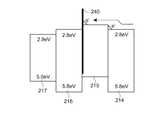
図4は、1つの色に対応する有機EL素子17を構成する積層構造を示す模式断面図である。以下に説明する有機EL素子17は、例えばカラーフィルタ200(R,G,B)を含めて構成されるカバー層21と、光透過可能な基板本体20を含む基板20A上に形成され、基板20A側に光を出射するいわゆるボトムエミッション構成を有している。 FIG. 4 is a schematic cross-sectional view showing a laminated structure constituting the
基板20A上には、ITOを用いてなる光学的に透明な陽極220が配置される。陽極220の層厚は、例えば100nm程度の値が用いられる。そして、陽極220上には、銅フタロシアニン(CuPc)を用いてなる正孔注入層219が配置される。正孔注入層219の層厚は、例えば10nm程度である。そして、正孔注入層219上には、例えば4,4’−ビス[N−(1−ナフチル)]−N−フェニルアミノ]ビフェニル(α−NPD)を用いてなる正孔輸送層218が配置される。正孔輸送層218の層厚は、例えば40nm程度である。そして、正孔輸送層218上には、アルミキノリノール錯体(Alq3)+ルブレン(5,6,11,12−テトラフェニルテトラセン)+ジシアノメチレンピラン誘導体(DCM2)を用いてなる赤色発光層217が配置される。赤色発光層217の層厚は、例えば5nm程度である。そして、赤色発光層217上には、BH215+BD102(共に出光興産製)を用いた青色発光層216が配置される。青色発光層216の層厚は、例えば10nm程度である。 An optically
そして、青色発光層216上には、例えばHT320(出光興産製)をホストとして、正孔トラップ性ドーパント及び/又は電子トラップ性ドーパントが添加されるキャリア調整層215が配置される。 On the blue
正孔トラップ性ドーパントとしては、イオン化ポテンシャルが比較的小さな化合物であることから、縮合環を有する芳香族アミン誘導体又はスチリルアミン誘導体が好ましく、例えば、図8に記載される化合物が好ましい。なお、図8中、Ar2〜Ar4は置換もしくは無置換の核炭素数6〜50の芳香族環、又は、置換もしくは無置換の核原子数5〜50の複素芳香族環であり、lは1〜4の整数である。lが2以上の場合、Ar3及びAr4はそれぞれ同じでも異なっていてもよい。Ar2〜Ar4のうち少なくとも一つは、置換もしくは無置換の核炭素数10〜50の縮合芳香族環又はスチリル基を有する。 As the hole trapping dopant, an aromatic amine derivative or a styrylamine derivative having a condensed ring is preferable because it is a compound having a relatively small ionization potential. For example, the compound shown in FIG. 8 is preferable. In FIG. 8, Ar2 to Ar4 are substituted or unsubstituted aromatic rings having 6 to 50 nuclear carbon atoms, or substituted or unsubstituted heteroaromatic rings having 5 to 50 nuclear atoms, and l is 1 It is an integer of ~ 4. When l is 2 or more, Ar3 and Ar4 may be the same or different. At least one of Ar2 to Ar4 has a substituted or unsubstituted condensed aromatic ring having 10 to 50 nuclear carbon atoms or a styryl group.
また、電子トラップ性ドーパントとしては、電子に対して安定であることから、置換もしくは無置換の核炭素数14〜50の縮合芳香族環化合物、又は核原子数5〜50の複素芳香族環化合物が好ましく、例えば、図9に記載される化合物が好ましい。なお、図9中、Ar5は核炭素数14〜50の芳香族環、もしくは核原子数5〜50の複素芳香族環であり、R2は置換基である。pは1〜6の整数、qは0〜30の整数である。pが2以上の場合、Ar5はそれぞれ同じでも異なっていてもよい。qが2以上の場合、R2はそれぞれ同じでも異なっていてもよい。キャリア調整層215の層厚は、例えば5nm程度である。 Moreover, as an electron-trapping dopant, since it is stable with respect to electrons, it is a substituted or unsubstituted condensed aromatic ring compound having 14 to 50 nuclear carbon atoms, or a heteroaromatic ring compound having 5 to 50 nuclear atoms. For example, the compound described in FIG. 9 is preferable. In FIG. 9, Ar5 is an aromatic ring having 14 to 50 nuclear carbon atoms or a heteroaromatic ring having 5 to 50 nuclear atoms, and R2 is a substituent. p is an integer of 1-6, q is an integer of 0-30. When p is 2 or more, Ar5 may be the same or different. When q is 2 or more, R2 may be the same or different. The layer thickness of the
そして、キャリア調整層215の上には、BH215+GD206(共に出光興産製)が緑色発光層214として配置される。緑色発光層214の層厚は、例えば10nm程度である。そして、緑色発光層214上には、Alq3を用いてなる電子輸送層213が配置される。電子輸送層213の層厚は例えば20nm程度である。そして、電子輸送層213上には、フッ化リチウム(LiF)を用いてなる電子注入層212が配置される。電子注入層212の層厚は、例えば1nm程度である。そして、電子注入層212上にはアルミニウム(Al)を用いてなる陰極211が形成されており、層厚は、例えば100nm程度の厚さを有している。 On the
(有機EL素子:正孔トラップ性ドーパントを用いる実施形態)
以下、キャリア調整層215が正孔トラップ性ドーパントを含む場合について説明を続ける。
図5は、赤色発光層217、青色発光層216、キャリア調整層215、緑色発光層214のエネルギーダイヤグラムである。ここで、キャリア調整層215は、正孔トラップ性ドーパントを含んでいる。そして、青色発光層216と緑色発光層214に挟まれる領域に位置し、かつ青色発光層216と接する端部に正孔トラップ性ドーパント濃度が最大値を取るよう配置されている。(Organic EL element: Embodiment using a hole trapping dopant)
Hereinafter, the case where the
FIG. 5 is an energy diagram of the red
そのため、図5に示すように、青色発光層216とキャリア調整層215との界面には正孔h+に対する正孔バリア230が形成される。また、赤色発光層217と青色発光層216との界面にも正孔h+に対するバリアが形成され、さらにキャリア調整層215と緑色発光層214との界面にも正孔h+に対するバリアが形成される。そのため、赤色発光層217、青色発光層216、緑色発光層214がそれぞれ正孔h+に対するバリアを有し、正孔h+をせき止める構造が得られる。そのため、赤色発光、青色発光、そして緑色発光とを強度バランス良く発光させることができる。即ち、R,G,B全色をバランス良く発光させることができる。Therefore, as shown in FIG. 5, a
R,G,Bのバランスが悪く、例えばGの発光強度が弱い場合には、RとBを強く発光させてRとBの発光成分に含まれるG成分をカラーフィルタにより抽出させて補正させることが必要となる。そのため、RとBとを構成する青色発光層216と赤色発光層217の寿命が縮まり、早期劣化を引き起こす。 When the balance of R, G, and B is poor, for example, when the emission intensity of G is weak, R and B are emitted strongly, and the G component included in the emission components of R and B is extracted by a color filter and corrected. Is required. Therefore, the lifetimes of the blue
本実施形態によれば、R,G,B全色をバランス良く発光させることができる。そのため、赤色発光層217、青色発光層216、緑色発光層214のいずれかの発光強度を無理に上げ、各波長の裾での発光を用いて色バランスをとる必要がなくなり、各発光層の寿命を長く保つことができる。 According to this embodiment, R, G, and B colors can be emitted with a good balance. Therefore, it is not necessary to forcibly increase the light emission intensity of any of the red
また、正孔h+が蓄積されている発光部では電子eの注入量により発光強度が支配される。そのため、発光強度は駆動電流強度に対して高い相関性を持ち、駆動電流強度の上昇に対して光強度は線形性を持って上昇するため、光強度の制御を容易に行うことができる。In the light emitting part in which holes h+ are accumulated, the light emission intensity is governed by the injection amount of electrons e. Therefore, the light emission intensity has a high correlation with the drive current intensity, and the light intensity increases with linearity as the drive current intensity increases, so that the light intensity can be easily controlled.
また、発光部の位置変動が抑えられる(界面に限定される)。そのため、輝度を変動させる場合においても、色純度や色相の変動を抑えることが可能となる。従って、色再現性に優れた有機EL素子17を提供することが可能となる。 Further, the position variation of the light emitting part is suppressed (limited to the interface). Therefore, even when the luminance is varied, it is possible to suppress variations in color purity and hue. Therefore, it is possible to provide the
また、正孔トラップ性ドーパントの濃度は、キャリア調整層215の端部以外の場所で最大値を取っても良い。例えばキャリア調整層215の青色発光層216と接する端部から離れた場所で濃度の最大値を与えることで、青色発光層216と比べ緑色発光層214により多くの正孔を供給することが可能となり、正孔トラップ性ドーパントの濃度分布を調整することで色バランスを制御することができる。 Further, the concentration of the hole trapping dopant may take a maximum value at a place other than the end of the
また、キャリア調整層215中での正孔トラップ性ドーパント密度を略均一にしても良い。この場合には、正孔トラップ性ドーパント密度によりキャリア調整層215が有するポテンシャル高さを制御することができ、ポテンシャル高さにより発生するホールバリア特性と、有機EL素子17の駆動電圧とを制御することができ、発光効率の最適化が容易となる。 Further, the hole trapping dopant density in the
(有機EL素子:電子トラップ性ドーパントを用いる実施形態)
以下、キャリア調整層215が電子トラップ性ドーパントを含む場合について説明する。積層構造等は上記したものと同一であり、重複を避けるため記載を省略する。
図6は、赤色発光層217、青色発光層216、キャリア調整層215、緑色発光層214のエネルギーダイヤグラムである。ここで、キャリア調整層215は、電子トラップ性ドーパントを含んでいる。そして、青色発光層216と緑色発光層214に挟まれる領域に位置し、かつ青色発光層216と接する端部に電子トラップ性ドーパント濃度が最大値を取るよう配置されている。そのため、図6に示すように、青色発光層216とキャリア調整層215との界面には電子e-に対する電子バリア240が形成される。(Organic EL element: Embodiment using electron trapping dopant)
Hereinafter, a case where the
FIG. 6 is an energy diagram of the red
この場合、青色発光層216側に電子が蓄積されるため、青色発光層216の発光効率を向上させることができる。また、キャリア調整層215中での電子トラップ性ドーパントの濃度は、キャリア調整層215の端部以外の場所で最大値を取っても良い。例えばキャリア調整層215の青色発光層216と接する端部から離れた場所で濃度の最大値を与えることで、青色発光層216と比べ緑色発光層214により多くの電子を供給することが可能となり、電子トラップ性ドーパントの濃度分布を調整することで色バランスを制御することができる。 In this case, since electrons are accumulated on the blue
また、キャリア調整層215中での電子トラップ性ドーパント密度を略均一にしても良い。この場合には、電子トラップ性ドーパント密度によりキャリア調整層215が有するポテンシャル高さを制御することができ、ポテンシャル高さにより発生する電子バリア特性と、有機EL素子17の駆動電圧とを制御することができ、発光効率の最適化が容易となる。 Further, the electron trapping dopant density in the
(変形例)
上記した実施形態では、キャリア調整層215を青色発光層216と緑色発光層214により挟持される位置に配置したが、これは赤色発光層217と青色発光層216との間に配置しても良い。また、赤色発光層217、青色発光層216、緑色発光層214はこの順に配置される必要はなく、発光層の順序はランダムに設定しても良い。また、キャリア調整層215は1層のみ配置されているが、これは各発光層に挟まれる位置に配置することができ、三原色の発光層中に2層設けても良い。
また、本実施形態では、陽極220としてITOを用いる例について説明したが、陽極220は導電性がある透明な素材を用いることが可能であり例えば、SnO2、Sb含有SnO2、Al含有ZnOなどの酸化物や、Au、Pt、Ag、Cu又はこれらを含む合金などや、ポリチオフェン、ポリピロールなどの導電性樹脂材料を用いることが可能である。(Modification)
In the above-described embodiment, the
Further, in this embodiment, an example in which ITO is used as the
また、正孔注入層219としてCuPcを用いる例について説明したが、これは、CuPcに代えて、4,4’,4’’−トリス(N,N−フェニル−3−メチルフェニルアミノ)トリフェニルアミン(m−MTDATA)等を用いることが可能である。 Moreover, although the example which uses CuPc as the
また、正孔輸送層218としてα−NPDを用いる例について説明したが、これは低分子の正孔輸送材料としては、例えば、1,1−ビス(4−ジ−パラ−トリアミノフェニル)シクロへキサン、1,1’−ビス(4−ジ−パラ−トリルアミノフェニル)−4−フェニル−シクロヘキサンのようなアリールシクロアルカン系化合物、4,4’,4’’−トリメチルトリフェニルアミン、N,N,N’,N’−テトラフェニル−1,1’−ビフェニル−4,4’−ジアミン、N,N’−ジフェニル−N,N’−ビス(3−メチルフェニル)−1,1’−ビフェニル−4,4’−ジアミン(TPD1)、N,N’−ジフェニル−N,N’−ビス(3−メトキシフェニル)−1,1’−ビフェニル−4,4’−ジアミン(TPD2)、N,N,N’,N’−テトラキス(4−メトキシフェニル)−1,1’−ビフェニル−4,4’−ジアミン(TPD3)、TPTE、4,4’,4’’−トリス(1−ナフチルフェニルアミノ)トリフェニルアミン(1−TNATA)のようなアリールアミン系化合物、N,N,N’,N’−テトラフェニル−パラ−フェニレンジアミン、N,N,N’,N’−テトラ(パラ−トリル)−パラ−フェニレンジアミン、N,N,N’,N’−テトラ(メタ−トリル)−メタ−フェニレンジアミン(PDA)のようなフェニレンジアミン系化合物、カルバゾール、N−イソプロピルカルバゾール、N−フェニルカルバゾールのようなカルバゾール系化合物、スチルベン、4−ジ−パラ−トリルアミノスチルベンのようなスチルベン系化合物、OxZのようなオキサゾール系化合物、トリフェニルメタン、m−MTDATAのようなトリフェニルメタン系化合物、1−フェニル−3−(パラ−ジメチルアミノフェニル)ピラゾリンのようなピラゾリン系化合物、ベンジン(シクロヘキサジエン)系化合物、トリアゾールのようなトリアゾール系化合物、イミダゾールのようなイミダゾール系化合物、1,3,4−オキサジアゾール、2,5−ジ(4−ジメチルアミノフェニル)−1,3,4,−オキサジアゾールのようなオキサジアゾール系化合物、アントラセン、9−(4−ジエチルアミノスチリル)アントラセンのようなアントラセン系化合物、フルオレノン、2,4,7,−トリニトロ−9−フルオレノン、2,7−ビス(2−ヒドロキシ−3−(2−クロロフェニルカルバモイル)−1−ナフチルアゾ)フルオレノンのようなフルオレノン系化合物、ポリアニリンのようなアニリン系化合物、シラン系化合物、1,4−ジチオケト−3,6−ジフェニル−ピロロ−(3,4−c)ピロロピロールのようなピロール系化合物、フローレンのようなフローレン系化合物、ポルフィリン、金属テトラフェニルポルフィリンのようなポルフィリン系化合物、キナクリドンのようなキナクリドン系化合物、フタロシアニン、銅フタロシアニン、テトラ(t−ブチル)銅フタロシアニン、鉄フタロシアニンのような金属又は無金属のフタロシアニン系化合物、銅ナフタロシアニン、バナジルナフタロシアニン、モノクロロガリウムナフタロシアニンのような金属又は無金属のナフタロシアニン系化合物、N,N’−ジ(ナフタレン−1−イル)−N,N’−ジフェニル−ベンジジン、N,N,N’,N’−テトラフェニルベンジジンのようなベンジジン系化合物等を用いることができる。低分子系の材料を用いる場合、例えば蒸着法を用いて正孔輸送層218を形成することが可能となる。 In addition, although an example in which α-NPD is used as the hole transport layer 218 has been described, as a low molecular weight hole transport material, for example, 1,1-bis (4-di-para-triaminophenyl) cyclo Hexane, arylcycloalkane compounds such as 1,1′-bis (4-di-para-tolylaminophenyl) -4-phenyl-cyclohexane, 4,4 ′, 4 ″ -trimethyltriphenylamine, N , N, N ′, N′-tetraphenyl-1,1′-biphenyl-4,4′-diamine, N, N′-diphenyl-N, N′-bis (3-methylphenyl) -1,1 ′ -Biphenyl-4,4'-diamine (TPD1), N, N'-diphenyl-N, N'-bis (3-methoxyphenyl) -1,1'-biphenyl-4,4'-diamine (TPD2), N, N, N ' N′-tetrakis (4-methoxyphenyl) -1,1′-biphenyl-4,4′-diamine (TPD3), TPTE, 4,4 ′, 4 ″ -tris (1-naphthylphenylamino) triphenylamine Arylamine compounds such as (1-TNATA), N, N, N ′, N′-tetraphenyl-para-phenylenediamine, N, N, N ′, N′-tetra (para-tolyl) -para- Phenylenediamine compounds such as phenylenediamine, N, N, N ′, N′-tetra (meta-tolyl) -meta-phenylenediamine (PDA), carbazole such as carbazole, N-isopropylcarbazole, N-phenylcarbazole Compounds, stilbenes, stilbene compounds such as 4-di-para-tolylaminostilbene, oxys such as OxZ Sazole compound, triphenylmethane, triphenylmethane compound such as m-MTDATA, pyrazoline compound such as 1-phenyl-3- (para-dimethylaminophenyl) pyrazoline, benzine (cyclohexadiene) compound, triazole Such as triazole-based compounds, imidazole-based compounds such as imidazole, 1,3,4-oxadiazole, 2,5-di (4-dimethylaminophenyl) -1,3,4, -oxadiazole Oxadiazole compounds, anthracene, anthracene compounds such as 9- (4-diethylaminostyryl) anthracene, fluorenone, 2,4,7, -trinitro-9-fluorenone, 2,7-bis (2-hydroxy-) 3- (2-Chlorophenylcarbamoyl) -1-naphthy Azo) fluorenone compounds such as fluorenone, aniline compounds such as polyaniline, silane compounds, pyrrole compounds such as 1,4-dithioketo-3,6-diphenyl-pyrrolo- (3,4-c) pyrrolopyrrole Compounds, fluorene compounds such as fluorene, porphyrins, porphyrin compounds such as metal tetraphenylporphyrin, quinacridone compounds such as quinacridone, phthalocyanine, copper phthalocyanine, tetra (t-butyl) copper phthalocyanine, iron phthalocyanine Metal or metal-free phthalocyanine compounds, copper naphthalocyanine, vanadyl naphthalocyanine, metal or metal-free naphthalocyanine compounds such as monochlorogallium naphthalocyanine, N, N′-di (naphthalen-1-yl) -N N'- diphenyl - benzidine, N, N, N ', can be used N'- benzidine compounds such as tetraphenyl benzidine. In the case of using a low molecular material, the
一方、高分子系の正孔輸送材料としては、例えば、ポリアリールアミンのようなアリールアミン骨格を有するもの、フルオレン−ビチオフェン共重合体のようなフルオレン骨格を有するもの、フルオレン−アリールアミン共重合体のようなアリールアミン骨格及びフルオレン骨格の双方を有するもの、ポリ(N−ビニルカルバゾール)、ポリビニルピレン、ポリビニルアントラセン、ポリチオフェン、ポリアルキルチオフェン、ポリヘキシルチオフェン、ポリ(p−フェニレンビニレン)、ポリチニレンビニレン、ピレンホルムアルデヒド樹脂、エチルカルバゾールホルムアルデヒド樹脂又はその誘導体等を用いることができる。高分子系の正孔輸送材料を用いる場合には、スピンコート法やインクジェット法により正孔輸送層218を形成することが可能となる。 On the other hand, examples of the polymer-based hole transport material include those having an arylamine skeleton such as polyarylamine, those having a fluorene skeleton such as a fluorene-bithiophene copolymer, and fluorene-arylamine copolymers. Having both an arylamine skeleton and a fluorene skeleton, such as poly (N-vinylcarbazole), polyvinylpyrene, polyvinylanthracene, polythiophene, polyalkylthiophene, polyhexylthiophene, poly (p-phenylenevinylene), polytinylene Vinylene, pyrene formaldehyde resin, ethylcarbazole formaldehyde resin or a derivative thereof can be used. When a polymer-based hole transport material is used, the
また、赤色発光層217、青色発光層216、緑色発光層214としてAlq3+ルブレン+DCM2、BH215(出光興産製)+BD102(出光興産製)、BH215(出光興産製)+GD206(出光興産製)を用いる例について説明している。この場合、これらの発光材料に代えて、例えば低分子の発光材料として、ジスチリルベンゼン(DSB)、ジアミノジスチリルベンゼン(DADSB)のようなベンゼン系化合物、ナフタレン、ナイルレッドのようなナフタレン系化合物、フェナントレンのようなフェナントレン系化合物、クリセン、6−ニトロクリセンのようなクリセン系化合物、ペリレン、N,N’−ビス(2,5−ジ−t−ブチルフェニル)−3,4,9,10−ペリレン−ジ−カルボキシイミド(BPPC)のようなペリレン系化合物、コロネンのようなコロネン系化合物、アントラセン、ビススチリルアントラセンのようなアントラセン系化合物、ピレンのようなピレン系化合物、4−(ジ−シアノメチレン)−2−メチル−6−(パラ−ジメチルアミノスチリル)−4H−ピラン(DCM)のようなピラン系化合物、アクリジンのようなアクリジン系化合物、スチルベンのようなスチルベン系化合物、2,5−ジベンゾオキサゾールチオフェンのようなチオフェン系化合物、ベンゾオキサゾールのようなベンゾオキサゾール系化合物、ベンゾイミダゾールのようなベンゾイミダゾール系化合物、2,2’−(パラ−フェニレンジビニレン)−ビスベンゾチアゾールのようなベンゾチアゾール系化合物、ビスチリル(1,4−ジフェニル−1,3−ブタジエン)、テトラフェニルブタジエンのようなブタジエン系化合物、ナフタルイミドのようなナフタルイミド系化合物、クマリンのようなクマリン系化合物、ペリノンのようなペリノン系化合物、オキサジアゾールのようなオキサジアゾール系化合物、アルダジン系化合物、1,2,3,4,5−ペンタフェニル−1,3−シクロペンタジエン(PPCP)のようなシクロペンタジエン系化合物、キナクリドン、キナクリドンレッドのようなキナクリドン系化合物、ピロロピリジン、チアジアゾロピリジンのようなピリジン系化合物、2,2’,7,7’−テトラフェニル−9,9’−スピロビフルオレンのようなスピロ化合物、フタロシアニン(H2Pc)、銅フタロシアニンのような金属又は無金属のフタロシアニン系化合物、フローレンのようなフローレン系化合物、トリス(4−メチル−8キノリノレート)アルミニウム(III)(Almq3)、8−ヒドロキシキノリン亜鉛(Znq2)、(1,10−フェナントロリン)−トリス−(4,4,4−トリフルオロ−1−(2−チエニル)−ブタン−1,3−ジオネート)ユーロピウム(III)(Eu(TTA)3(phen))、ファクトリス(2−フェニルピリジン)イリジウム(Ir(ppy)3)、2,3,7,8,12,13,17,18−オクタエチル−21H,23H−ポルフィンプラチナム(II)のような各種金属錯体等を用いることが可能である。 In addition, examples of using Alq3 + rubrene + DCM2, BH215 (Idemitsu Kosan) + BD102 (Idemitsu Kosan), BH215 (Idemitsu Kosan) + GD206 (Idemitsu Kosan) as the red
また、高分子の発光材料としては、例えば、トランス型ポリアセチレン、シス型ポリアセチレン、ポリ(ジ−フェニルアセチレン)(PDPA)、ポリ(アルキル,フェニルアセチレン)(PAPA)のようなポリアセチレン系化合物、ポリ(パラ−フェンビニレン)(PPV)、ポリ(2,5−ジアルコキシ−パラ−フェニレンビニレン)(RO−PPV)、シアノ−置換−ポリ(パラ−フェンビニレン)(CN−PPV)、ポリ(2−ジメチルオクチルシリル−パラ−フェニレンビニレン)(DMOS−PPV)、ポリ(2−メトキシ,5−(2’−エチルヘキソキシ)−パラ−フェニレンビニレン)(MEH−PPV)のようなポリパラフェニレンビニレン系化合物、ポリ(3−アルキルチオフェン)(PAT)、ポリ(オキシプロピレン)トリオール(POPT)のようなポリチオフェン系化合物、ポリ(9,9−ジアルキルフルオレン)(PDAF)、α,ω−ビス[N,N’−ジ(メチルフェニル)アミノフェニル]−ポリ[9,9−ビス(2−エチルヘキシル)フルオレン−2,7−ジル](PF2/6am4)、ポリ(9,9−ジオクチル−2,7−ジビニレンフルオレニル−オルト−コ(アントラセン−9,10−ジイル)のようなポリフルオレン系化合物、ポリ(パラ−フェニレン)(PPP)、ポリ(1,5−ジアルコキシ−パラ−フェニレン)(RO−PPP)のようなポリパラフェニレン系化合物、ポリ(N−ビニルカルバゾール)(PVK)のようなポリカルバゾール系化合物、ポリ(メチルフェニルシラン)(PMPS)、ポリ(ナフチルフェニルシラン)(PNPS)、ポリ(ビフェニリルフェニルシラン)(PBPS)のようなポリシラン系化合物等を用いることが可能である。 Examples of the polymer luminescent material include polyacetylene compounds such as trans-polyacetylene, cis-polyacetylene, poly (di-phenylacetylene) (PDPA), poly (alkyl, phenylacetylene) (PAPA), and poly ( Para-phenvinylene) (PPV), poly (2,5-dialkoxy-para-phenylenevinylene) (RO-PPV), cyano-substituted-poly (para-phenvinylene) (CN-PPV), poly (2- Polyparaphenylene vinylene compounds such as dimethyloctylsilyl-para-phenylene vinylene (DMOS-PPV), poly (2-methoxy, 5- (2′-ethylhexoxy) -para-phenylene vinylene) (MEH-PPV), Poly (3-alkylthiophene) (PAT), poly (oxypropioxy) Polythiophene-based compounds such as N) triol (POPT), poly (9,9-dialkylfluorene) (PDAF), α, ω-bis [N, N′-di (methylphenyl) aminophenyl] -poly [9, 9-bis (2-ethylhexyl) fluorene-2,7-diyl] (PF2 / 6am4), poly (9,9-dioctyl-2,7-divinylenefluorenyl-ortho-co (anthracene-9,10-) Polyfluorene compounds such as diyl), poly (para-phenylene) (PPP), polyparaphenylene compounds such as poly (1,5-dialkoxy-para-phenylene) (RO-PPP), poly (N -Polycarbazole compounds such as (vinylcarbazole) (PVK), poly (methylphenylsilane) (PMPS), poly (naphthylphenylsilane) Down) (PnPs), it is possible to use a polysilane compound such as poly (biphenylyl phenyl silane) (pBPS) or the like.
また、電子輸送層213としてAlq3を用いる例について説明したが、これは1,3,5−トリス[(3−フェニル−6−トリ−フルオロメチル)キノキサリン−2−イル]ベンゼン(TPQ1)、1,3,5−トリス[{3−(4−t−ブチルフェニル)−6−トリスフルオロメチル}キノキサリン−2−イル]ベンゼン(TPQ2)のようなベンゼン系化合物(スターバースト系化合物)、ナフタレンのようなナフタレン系化合物、フェナントレンのようなフェナントレン系化合物、クリセンのようなクリセン系化合物、ペリレンのようなペリレン系化合物、アントラセンのようなアントラセン系化合物、ピレンのようなピレン系化合物、アクリジンのようなアクリジン系化合物、スチルベンのようなスチルベン系化合物、BBOTのようなチオフェン系化合物、ブタジエンのようなブタジエン系化合物、クマリンのようなクマリン系化合物、キノリンのようなキノリン系化合物、ビスチリルのようなビスチリル系化合物、ピラジン、ジスチリルピラジンのようなピラジン系化合物、キノキサリンのようなキノキサリン系化合物、ベンゾキノン、2,5−ジフェニル−パラ−ベンゾキノンのようなベンゾキノン系化合物、ナフトキノンのようなナフトキノン系化合物、アントラキノンのようなアントラキノン系化合物、オキサジアゾール、2−(4−ビフェニリル)−5−(4−t−ブチルフェニル)−1,3,4−オキサジアゾール(PBD)、BMD、BND、BDD、BAPDのようなオキサジアゾール系化合物、トリアゾール、3,4,5−トリフェニル−1,2,4−トリアゾールのようなトリアゾール系化合物、オキサゾール系化合物、アントロンのようなアントロン系化合物、フルオレノン、1,3,8−トリニトロ−フルオレノン(TNF)のようなフルオレノン系化合物、ジフェノキノン、MBDQのようなジフェノキノン系化合物、スチルベンキノン、MBSQのようなスチルベンキノン系化合物、アントラキノジメタン系化合物、チオピランジオキシド系化合物、フルオレニリデンメタン系化合物、ジフェニルジシアノエチレン系化合物、フローレンのようなフローレン系化合物、フタロシアニン、銅フタロシアニン、鉄フタロシアニンのような金属又は無金属のフタロシアニン系化合物、ベンゾオキサゾールやベンゾチアゾールを配位子とする錯体のような各種金属錯体等を用いることが可能である。また、オキサジアゾール系高分子(ポリオキサジアゾール)、トリアゾール系高分子(ポリトリアゾール)等の高分子系の材料を用いても良い。 In addition, an example in which Alq3 is used as the electron transporting layer 213 has been described, which is 1,3,5-tris [(3-phenyl-6-tri-fluoromethyl) quinoxalin-2-yl] benzene (TPQ1), 1 , 3,5-tris [{3- (4-t-butylphenyl) -6-trisfluoromethyl} quinoxalin-2-yl] benzene (TPQ2), a benzene compound (starburst compound), naphthalene Naphthalene compounds such as phenanthrene, chrysene compounds such as chrysene, perylene compounds such as perylene, anthracene compounds such as anthracene, pyrene compounds such as pyrene, acridine Acridine compounds, stilbene compounds such as stilbene, BBOT Thiophene compounds, butadiene compounds such as butadiene, coumarin compounds such as coumarin, quinoline compounds such as quinoline, bistyryl compounds such as bistyryl, pyrazine compounds such as pyrazine and distyrylpyrazine, quinoxaline Quinoxaline compounds such as benzoquinone, benzoquinone compounds such as 2,5-diphenyl-para-benzoquinone, naphthoquinone compounds such as naphthoquinone, anthraquinone compounds such as anthraquinone, oxadiazole, 2- (4- Biphenylyl) -5- (4-t-butylphenyl) -1,3,4-oxadiazole (PBD), oxadiazole compounds such as BMD, BND, BDD, BAPD, triazole, 3,4,5 -Triphenyl-1,2, -Triazole compounds such as triazole, oxazole compounds, anthrone compounds such as anthrone, fluorenones, fluorenone compounds such as 1,3,8-trinitro-fluorenone (TNF), diphenoquinones such as diphenoquinone and MBDQ Compounds, stilbene quinones, stilbene quinone compounds such as MBSQ, anthraquinodimethane compounds, thiopyrandioxide compounds, fluorenylidene methane compounds, diphenyldicyanoethylene compounds, fluorene compounds such as fluorene, phthalocyanines Various metal complexes such as metal or metal-free phthalocyanine compounds such as copper phthalocyanine and iron phthalocyanine, and complexes having benzoxazole and benzothiazole as a ligand can be used. Noh. Further, polymer materials such as oxadiazole polymer (polyoxadiazole) and triazole polymer (polytriazole) may be used.
また、電子注入層212としてLiFを用いる例について説明したが、これは無機絶縁材料としては、例えば、アルカリ金属カルコゲナイド(酸化物、硫化物、セレン化物、テルル化物)、アルカリ土類金属カルコゲナイド、アルカリ金属のハロゲン化物及びアルカリ土類金属のハロゲン化物等が挙げられ、これらのうちの1種又は2種以上を組み合わせて用いることができる。これらを主材料として電子注入層を構成することにより、電子注入性をより向上させることができる。アルカリ金属カルコゲナイドとしては、例えば、Li2O、LiO、Na2S、Na2Se、NaO等が挙げられる。アルカリ土類金属カルコゲナイドとしては、例えば、CaO、BaO、SrO、BeO、BaS、MgO、CaSe等が挙げられる。アルカリ金属のハロゲン化物としては、例えば、CsF、NaF、KF、LiCl、KCl、NaCl等が挙げられる。アルカリ土類金属のハロゲン化物としては、例えば、CaF2、BaF2、SrF2、MgF2、BeF2等が挙げられる。In addition, although an example in which LiF is used as the
また、無機半導体材料としては、例えば、Ba、Ca、Sr、Yb、Al、Ga、In、Li、Na、Cd、Mg、Si、Ta、Sb及びZnのうちの少なくとも1つの元素を含む酸化物、窒化物又は酸化窒化物等が挙げられ、これらのうちの1種又は2種以上を組み合わせて用いることができる。 Moreover, as an inorganic semiconductor material, for example, an oxide containing at least one element of Ba, Ca, Sr, Yb, Al, Ga, In, Li, Na, Cd, Mg, Si, Ta, Sb, and Zn , Nitrides, oxynitrides, and the like, and one or more of these can be used in combination.
また、有機材料としては、例えば、8−ヒドロキシキノリン、オキサジアゾール、又は、これらの誘導体(例えば、8−ヒドロキシキノリンを含む金属キレートオキシノイド化合物)等が挙げられ、これらのうちの1種又は2種以上組み合わせて(例えば、複数層の積層体等として)用いることが可能である。 In addition, examples of the organic material include 8-hydroxyquinoline, oxadiazole, or derivatives thereof (for example, metal chelate oxinoid compounds containing 8-hydroxyquinoline). Two or more types can be used in combination (for example, as a multi-layer laminate).
また、陰極211としてアルミニウム(Al)を用いる例について説明したが、これは、Li、Mg、Ca、Sr、La、Ce、Er、Eu、Sc、Y、Yb、Ag、Cu、Cs、Rb又は、これら及びAlを含む合金等が挙げられ、これらのうちの少なくとも1種を用いることができる。 Moreover, although the example which uses aluminum (Al) as the
(電子機器への搭載例)
以下、図7を参照して、上述したカラー有機ELディスプレイ1を含む電子機器について説明する。図7(a)に、カラー有機ELディスプレイ1を備えたモバイル型のパーソナルコンピュータの構成を示す。パーソナルコンピュータ2000は、カラー有機ELディスプレイ1と本体部2010を備える。本体部2010には、電源スイッチ2001及びキーボード2002が設けられている。(Example of mounting on electronic equipment)
Hereinafter, with reference to FIG. 7, an electronic apparatus including the above-described color
図7(b)に、カラー有機ELディスプレイ1を備えた携帯電話機の構成を示す。携帯電話機3000は、複数の操作ボタン3001及びスクロールボタン3002、並びに表示ユニットとしてのカラー有機ELディスプレイ1を備える。スクロールボタン3002を操作することによって、カラー有機ELディスプレイ1に表示される画面がスクロールされる。 FIG. 7B shows a configuration of a mobile phone provided with the color
図7(c)に、カラー有機ELディスプレイ1を適用した情報携帯端末(PDA)の構成を示す。情報携帯端末4000は、複数の操作ボタン4001及び電源スイッチ4002、並びに表示ユニットとしてのカラー有機ELディスプレイ1を備える。電源スイッチ4002を操作すると、住所録やスケジュール帳といった各種の情報がカラー有機ELディスプレイ1に表示される。 FIG. 7C shows the configuration of a portable information terminal (PDA) to which the color
なお、カラー有機ELディスプレイ1が搭載される電子機器としては、図7に示すものの他、デジタルスチルカメラ、液晶テレビ、ビューファインダ型、モニタ直視型のビデオテープレコーダ、カーナビゲーション装置、ページャ、電子手帳、電卓、ワードプロセッサ、ワークステーション、テレビ電話、POS端末、タッチパネルを備えた機器などが挙げられる。そして、これらの各種電子機器の表示部として、前述したカラー有機ELディスプレイ1が適用可能である。 The electronic devices on which the color
1…カラー有機ELディスプレイ、3…画素部、4…実表示領域、5…ダミー領域、17…有機EL素子、20…基板本体、20A…基板、21…カバー層、23…画素電極、40…サブ画素、41…表示単位画素、80…走査線駆動回路、90…検査回路、100…データ線駆動回路、101…走査線、102…信号線、103…電源線、113…保持容量、122…TFT、123…TFT、200…カラーフィルタ、211…陰極、212…電子注入層、213…電子輸送層、214…緑色発光層、215…キャリア調整層、216…青色発光層、217…赤色発光層、218…正孔輸送層、219…正孔注入層、220…陽極、230…正孔バリア、240…電子バリア、2000…パーソナルコンピュータ、2001…電源スイッチ、2002…キーボード、2010…本体部、3000…携帯電話機、3001…操作ボタン、3002…スクロールボタン、4000…情報携帯端末、4001…操作ボタン、4002…電源スイッチ、h+…正孔、e-…電子。DESCRIPTION OF
Claims (3)
Translated fromJapanese前記陽極及び前記陰極に狭持される複数の有機発光層と、
複数の前記有機発光層に挟持される単一又は複数の領域に対し、少なくともその一領域に配置されるキャリア調整層と、
前記キャリア調整層に配分される正孔トラップ性ドーパント及び/又は電子トラップ性ドーパントと、を含むことを特徴とするカラー有機ELディスプレイ。An anode and a cathode;
A plurality of organic light emitting layers sandwiched between the anode and the cathode;
For a single region or a plurality of regions sandwiched between a plurality of the organic light emitting layers, a carrier adjustment layer disposed in at least one region;
A color organic EL display comprising a hole trapping dopant and / or an electron trapping dopant distributed to the carrier adjustment layer.
Priority Applications (1)
| Application Number | Priority Date | Filing Date | Title |
|---|---|---|---|
| JP2007207509AJP2009043577A (en) | 2007-08-09 | 2007-08-09 | Color organic EL display and electronic device |
Applications Claiming Priority (1)
| Application Number | Priority Date | Filing Date | Title |
|---|---|---|---|
| JP2007207509AJP2009043577A (en) | 2007-08-09 | 2007-08-09 | Color organic EL display and electronic device |
Publications (1)
| Publication Number | Publication Date |
|---|---|
| JP2009043577Atrue JP2009043577A (en) | 2009-02-26 |
Family
ID=40444106
Family Applications (1)
| Application Number | Title | Priority Date | Filing Date |
|---|---|---|---|
| JP2007207509AWithdrawnJP2009043577A (en) | 2007-08-09 | 2007-08-09 | Color organic EL display and electronic device |
Country Status (1)
| Country | Link |
|---|---|
| JP (1) | JP2009043577A (en) |
Cited By (1)
| Publication number | Priority date | Publication date | Assignee | Title |
|---|---|---|---|---|
| JP2010218850A (en)* | 2009-03-16 | 2010-09-30 | Seiko Epson Corp | Light-emitting element, light-emitting device, display device and electronic equipment |
Citations (3)
| Publication number | Priority date | Publication date | Assignee | Title |
|---|---|---|---|---|
| JP2005135600A (en)* | 2003-10-28 | 2005-05-26 | Idemitsu Kosan Co Ltd | Organic electroluminescence light emitting device |
| JP2006172763A (en)* | 2004-12-13 | 2006-06-29 | Toyota Industries Corp | Organic el element |
| JP2006172762A (en)* | 2004-12-13 | 2006-06-29 | Toyota Industries Corp | Organic el element |
- 2007
- 2007-08-09JPJP2007207509Apatent/JP2009043577A/ennot_activeWithdrawn
Patent Citations (3)
| Publication number | Priority date | Publication date | Assignee | Title |
|---|---|---|---|---|
| JP2005135600A (en)* | 2003-10-28 | 2005-05-26 | Idemitsu Kosan Co Ltd | Organic electroluminescence light emitting device |
| JP2006172763A (en)* | 2004-12-13 | 2006-06-29 | Toyota Industries Corp | Organic el element |
| JP2006172762A (en)* | 2004-12-13 | 2006-06-29 | Toyota Industries Corp | Organic el element |
Cited By (1)
| Publication number | Priority date | Publication date | Assignee | Title |
|---|---|---|---|---|
| JP2010218850A (en)* | 2009-03-16 | 2010-09-30 | Seiko Epson Corp | Light-emitting element, light-emitting device, display device and electronic equipment |
Similar Documents
| Publication | Publication Date | Title |
|---|---|---|
| US8902136B2 (en) | Organic electroluminescence display device and method for driving the same | |
| KR100903918B1 (en) | Organic Electroluminescence Element and Display | |
| CN101404323B (en) | Light-emitting component, display unit and e-machine | |
| JP4915356B2 (en) | LIGHT EMITTING ELEMENT, DISPLAY DEVICE, AND ELECTRONIC DEVICE | |
| EP1441573A2 (en) | Organic electroluminiscent device | |
| JP2004185967A (en) | Organic electroluminescent element, its manufacturing method, display device, lighting system, and light source | |
| JP7543003B2 (en) | Organic light-emitting device, display device having the same, imaging device, lighting device, and mobile object | |
| US6897621B2 (en) | Three-terminal organic electro-luminescent device | |
| US9401492B2 (en) | Light-emitting element, light-emitting device, display device, and electronic apparatus | |
| JP2020184569A (en) | Organic light emitting element, display device having it, image pickup device, lighting device, mobile body | |
| CN101599535A (en) | Light emitting element, display device and electronic equipment | |
| JP2023107949A (en) | Organic light-emitting device, display device having same, imaging device, lighting device, moving object | |
| JP2005174675A (en) | Organic electroluminescent element and light emitting device | |
| JP4277816B2 (en) | LIGHT EMITTING ELEMENT, DISPLAY DEVICE, AND ELECTRONIC DEVICE | |
| JP2009043577A (en) | Color organic EL display and electronic device | |
| JP2009129711A (en) | LIGHT EMITTING ELEMENT, DISPLAY DEVICE, AND ELECTRONIC DEVICE | |
| WO2011024346A1 (en) | Organic electroluminescent element, organic electroluminescent display device, and organic electroluminescent illuminating device | |
| JP2009043576A (en) | Color organic EL display and electronic device | |
| JP2009301760A (en) | Light-emitting element, light-emitting device, light-emitting element manufacturing method, display device, and electronic equipment | |
| JP2011054461A (en) | Lighting apparatus, display device equipped with the same, and electronic device | |
| KR100601332B1 (en) | Organic semiconductor device, manufacturing method and manufacturing apparatus thereof | |
| JP2010050281A (en) | Light-emitting element, display device and electronic equipment | |
| JP2004164895A (en) | Organic electroluminescent element and display device |
Legal Events
| Date | Code | Title | Description |
|---|---|---|---|
| A621 | Written request for application examination | Free format text:JAPANESE INTERMEDIATE CODE: A621 Effective date:20100714 | |
| A977 | Report on retrieval | Free format text:JAPANESE INTERMEDIATE CODE: A971007 Effective date:20120110 | |
| A131 | Notification of reasons for refusal | Free format text:JAPANESE INTERMEDIATE CODE: A131 Effective date:20120117 | |
| A761 | Written withdrawal of application | Free format text:JAPANESE INTERMEDIATE CODE: A761 Effective date:20120214 |