JP2009021919A - Image pickup device - Google Patents
Image pickup deviceDownload PDFInfo
- Publication number
- JP2009021919A JP2009021919AJP2007184211AJP2007184211AJP2009021919AJP 2009021919 AJP2009021919 AJP 2009021919AJP 2007184211 AJP2007184211 AJP 2007184211AJP 2007184211 AJP2007184211 AJP 2007184211AJP 2009021919 AJP2009021919 AJP 2009021919A
- Authority
- JP
- Japan
- Prior art keywords
- imaging
- image
- microlens
- pixels
- aperture stop
- Prior art date
- Legal status (The legal status is an assumption and is not a legal conclusion. Google has not performed a legal analysis and makes no representation as to the accuracy of the status listed.)
- Granted
Links
- 238000003384imaging methodMethods0.000claimsdescription100
- 239000000284extractSubstances0.000claims1
- 230000004907fluxEffects0.000abstractdescription2
- 230000000593degrading effectEffects0.000abstract1
- 230000004048modificationEffects0.000description10
- 238000012986modificationMethods0.000description10
- 238000000605extractionMethods0.000description6
- 238000000034methodMethods0.000description4
- 239000011159matrix materialSubstances0.000description3
- 230000003287optical effectEffects0.000description3
- 230000000052comparative effectEffects0.000description2
- 230000000007visual effectEffects0.000description2
- 230000000295complement effectEffects0.000description1
- 238000010586diagramMethods0.000description1
- 239000006185dispersionSubstances0.000description1
- 230000000694effectsEffects0.000description1
- 239000007788liquidSubstances0.000description1
- 239000004973liquid crystal related substanceSubstances0.000description1
- 229910044991metal oxideInorganic materials0.000description1
- 150000004706metal oxidesChemical class0.000description1
- 239000000203mixtureSubstances0.000description1
- 239000004065semiconductorSubstances0.000description1
Images


Classifications
- G—PHYSICS
- G02—OPTICS
- G02B—OPTICAL ELEMENTS, SYSTEMS OR APPARATUS
- G02B27/00—Optical systems or apparatus not provided for by any of the groups G02B1/00 - G02B26/00, G02B30/00
- G02B27/0075—Optical systems or apparatus not provided for by any of the groups G02B1/00 - G02B26/00, G02B30/00 with means for altering, e.g. increasing, the depth of field or depth of focus
- H—ELECTRICITY
- H04—ELECTRIC COMMUNICATION TECHNIQUE
- H04N—PICTORIAL COMMUNICATION, e.g. TELEVISION
- H04N23/00—Cameras or camera modules comprising electronic image sensors; Control thereof
- H04N23/95—Computational photography systems, e.g. light-field imaging systems
- H04N23/957—Light-field or plenoptic cameras or camera modules
- G—PHYSICS
- G02—OPTICS
- G02B—OPTICAL ELEMENTS, SYSTEMS OR APPARATUS
- G02B3/00—Simple or compound lenses
- G02B3/0006—Arrays
- G02B3/0037—Arrays characterized by the distribution or form of lenses
- G02B3/0056—Arrays characterized by the distribution or form of lenses arranged along two different directions in a plane, e.g. honeycomb arrangement of lenses
- H—ELECTRICITY
- H04—ELECTRIC COMMUNICATION TECHNIQUE
- H04N—PICTORIAL COMMUNICATION, e.g. TELEVISION
- H04N25/00—Circuitry of solid-state image sensors [SSIS]; Control thereof
- H04N25/10—Circuitry of solid-state image sensors [SSIS]; Control thereof for transforming different wavelengths into image signals
- H04N25/11—Arrangement of colour filter arrays [CFA]; Filter mosaics
- H04N25/13—Arrangement of colour filter arrays [CFA]; Filter mosaics characterised by the spectral characteristics of the filter elements
- H04N25/134—Arrangement of colour filter arrays [CFA]; Filter mosaics characterised by the spectral characteristics of the filter elements based on three different wavelength filter elements
- H—ELECTRICITY
- H04—ELECTRIC COMMUNICATION TECHNIQUE
- H04N—PICTORIAL COMMUNICATION, e.g. TELEVISION
- H04N23/00—Cameras or camera modules comprising electronic image sensors; Control thereof
- H04N23/80—Camera processing pipelines; Components thereof
- H04N23/84—Camera processing pipelines; Components thereof for processing colour signals
- H04N23/843—Demosaicing, e.g. interpolating colour pixel values
Landscapes
- Physics & Mathematics (AREA)
- Engineering & Computer Science (AREA)
- Multimedia (AREA)
- Signal Processing (AREA)
- General Physics & Mathematics (AREA)
- Optics & Photonics (AREA)
- Spectroscopy & Molecular Physics (AREA)
- Computing Systems (AREA)
- Theoretical Computer Science (AREA)
- Studio Devices (AREA)
- Transforming Light Signals Into Electric Signals (AREA)
- Solid State Image Pick-Up Elements (AREA)
Abstract
Description
Translated fromJapanese本発明は、マイクロレンズアレイを用いた撮像装置に関する。 The present invention relates to an imaging apparatus using a microlens array.
従来、様々な撮像装置が提案され、開発されている。また、撮像して得られた撮像データに対し、所定の画像処理を施して出力するようにした撮像装置も提案されている。 Conventionally, various imaging devices have been proposed and developed. There has also been proposed an imaging apparatus that performs predetermined image processing on imaging data obtained by imaging and outputs the data.
例えば、特許文献1および非特許文献1には、「Light Field Photography」と呼ばれる手法を用いた撮像装置が提案されている。この撮像装置は、撮像レンズと、マイクロレンズアレイと、撮像素子と、画像処理部とから構成され、撮像レンズには中央部に単一の開口を有する開口絞りが設けられている。このような構成により、撮像素子から得られる撮像データが、受光面における光の強度分布に加えてその光の進行方向の情報をも含むようになっている。そして画像処理部において、任意の視点や方向(以下、単に視野という)からの観察画像を再構築できるようになっている。
ところで、上記マイクロレンズアレイには、複数のマイクロレンズが設けられており、各マイクロレンズに対して撮像素子の複数の画素が割り当てられるようになっている。そして上記手法を利用した場合には、再構築された画像の画素数はマイクロレンズアレイにおけるマイクロレンズ数と等しくなる。これは、再構築画像の2次元座標の情報がマイクロレンズアレイの座標で決まるためである。従って、再構成画像の2次元座標の画素数は撮像素子の全画素数を各マイクロレンズに割り当てられる画素数で割った数となる。一方、各マイクロレンズに割り当てられる画素数は、光線の角度情報の分解能に等しく、再構築画像の任意の視野における分解能、すなわち、どれだけ多くの視点や方向から画像が再構築されているかを決定する。このため、任意の視野における分解能と2次元座標の画素数とはトレードオフの関係にある。 By the way, the microlens array is provided with a plurality of microlenses, and a plurality of pixels of the image sensor are assigned to each microlens. When the above method is used, the number of pixels of the reconstructed image is equal to the number of microlenses in the microlens array. This is because the two-dimensional coordinate information of the reconstructed image is determined by the coordinates of the microlens array. Therefore, the number of pixels in the two-dimensional coordinates of the reconstructed image is the number obtained by dividing the total number of pixels of the image sensor by the number of pixels assigned to each microlens. On the other hand, the number of pixels assigned to each microlens is equal to the resolution of the angle information of the light rays, and determines the resolution in an arbitrary field of view of the reconstructed image, that is, how many viewpoints and directions are reconstructed. To do. For this reason, the resolution in an arbitrary field of view and the number of pixels of the two-dimensional coordinates are in a trade-off relationship.
従って、撮像素子の全画素数が一定である場合に、マイクロレンズの数を増やすことにより、撮像素子における各マイクロレンズへの画素数の割り当てが減り、これによって再構築画像の2次元座標の画素数を増やすことが可能である。 Accordingly, when the total number of pixels of the image sensor is constant, by increasing the number of microlenses, the allocation of the number of pixels to each microlens in the image sensor is reduced, and thereby the pixels of the two-dimensional coordinates of the reconstructed image It is possible to increase the number.
しかしながら、各マイクロレンズへ割り当てられる画素数を減らした場合、各画素で受光される光線の進行方向の分解能が低下し、所望の進行方向の光線情報を得にくくなってしまう。これにより、画像処理により再構築画像を生成した際に、その画質が低下するという問題がある。 However, when the number of pixels assigned to each microlens is reduced, the resolution in the traveling direction of the light received by each pixel is lowered, making it difficult to obtain light information in the desired traveling direction. As a result, there is a problem in that when a reconstructed image is generated by image processing, the image quality is degraded.
本発明はかかる問題点に鑑みてなされたもので、その目的は、画像処理によって再構築画像を生成する際に、その再構築画像の画質を低下させることなく画素数を増加させることが可能な撮像データを生成する撮像装置を提供することにある。 The present invention has been made in view of such problems, and an object thereof is to increase the number of pixels without reducing the image quality of the reconstructed image when the reconstructed image is generated by image processing. An object of the present invention is to provide an imaging device that generates imaging data.
本発明の撮像装置は、複数の開口部を含む開口絞りを有する撮像レンズ部と、受光した光に基づいて撮像データを生成する撮像素子と、撮像レンズ部と撮像素子との間で撮像レンズ部の焦点面上に配置されると共に、撮像素子の複数の画素に対して1つのマイクロレンズを有するマイクロレンズアレイ部とを備えたものである。 An imaging device of the present invention includes an imaging lens unit having an aperture stop including a plurality of apertures, an imaging element that generates imaging data based on received light, and an imaging lens unit between the imaging lens unit and the imaging element. And a microlens array section having one microlens for a plurality of pixels of the image sensor.
本発明の撮像装置では、撮像レンズ部による撮像対象物の像は、マイクロレンズアレイ部上に結像する。そしてこのマイクロレンズアレイ部へ入射した光線が撮像素子へ到達し、各マイクロレンズに対応する複数の画素で受光されることにより、光の進行方向の情報を含んだ撮像データが得られる。ここで、上記撮像レンズ部の開口絞りには複数の開口部が設けられていることにより、各開口部によって光束が絞られ、撮像素子では各開口部に対応する画素領域において受光がなされる。したがって、マイクロレンズの数を増やして各マイクロレンズに割り当てられる撮像素子の画素数を減らした場合であっても、一画素内では開口部によって光束が絞られて、進行方向が制限された光線のみが開口部を通過するため、撮像レンズの開口絞りに単一の開口部が設けられている従来と比べ、所望の進行方向の光線情報が得やすくなる。 In the imaging apparatus of the present invention, the image of the object to be imaged by the imaging lens unit is formed on the microlens array unit. Then, the light beam incident on the microlens array unit reaches the image sensor and is received by a plurality of pixels corresponding to each microlens, thereby obtaining image data including information on the light traveling direction. Here, since the aperture stop of the imaging lens unit is provided with a plurality of apertures, the light flux is focused by each aperture, and the image sensor receives light in the pixel region corresponding to each aperture. Therefore, even if the number of microlenses is increased and the number of pixels of the image sensor assigned to each microlens is reduced, only the light beam whose traveling direction is restricted by the aperture within one pixel is restricted. Passes through the aperture, so that it becomes easier to obtain light ray information in a desired traveling direction than in the conventional case where a single aperture is provided in the aperture stop of the imaging lens.
本発明の撮像装置によれば、撮像レンズの開口絞りが複数の開口部を含むようにしたので、マイクロレンズの数を増やして、各マイクロレンズに割り当てられる画素数を減らした場合であっても、撮像素子では各開口部によって光束が絞られて受光されるため、一画素内の受光領域において、所望の進行方向の光線情報を得易くなる。よって、画像処理を施して再構築画像を生成する際に、画質を低下させることなく、再構築画像の画素数を増加させることができる。 According to the imaging apparatus of the present invention, since the aperture stop of the imaging lens includes a plurality of apertures, even when the number of microlenses is increased and the number of pixels allocated to each microlens is reduced. In the image pickup device, the light beam is focused and received by each opening, so that it becomes easy to obtain light ray information in a desired traveling direction in the light receiving region in one pixel. Therefore, when generating a reconstructed image by performing image processing, the number of pixels of the reconstructed image can be increased without reducing the image quality.
以下、本発明の実施の形態について、図面を参照して詳細に説明する。 Hereinafter, embodiments of the present invention will be described in detail with reference to the drawings.
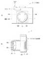
図1は、本発明の第1の実施の形態に係る撮像装置(撮像装置1)の全体構成を表したものである。この撮像装置1は、被写体2を撮像して撮像データDoutを出力するものであり、被写体2の側から、開口絞り10と、撮像レンズ11と、マイクロレンズアレイ12と、撮像素子13と、画像処理部14と、撮像素子駆動部15と、制御部16とから構成されている。 FIG. 1 shows the overall configuration of an imaging apparatus (imaging apparatus 1) according to a first embodiment of the present invention. This
開口絞り10は、撮像レンズ11の光学的な開口絞りである。この開口絞り10の詳細な構成については後述する。 The
撮像レンズ11は、被写体を撮像するためのメインレンズであり、例えば、ビデオカメラやスチルカメラ等で使用される一般的な撮像レンズにより構成される。 The
マイクロレンズアレイ12は、後述の複数のマイクロレンズが配列したものであり、撮像レンズ11の焦点面(図中の符号f1は、撮像レンズ11の焦点距離を表している)に配置されている。このマイクロレンズアレイ12の具体的な構成については後述する。 The
撮像素子13は、マイクロレンズアレイ12からの光を受光して撮像データを生成するものであり、マイクロレンズアレイ12の焦点面(図中の符号f2は、マイクロレンズアレイ12の焦点距離を表している)に配置されている。この撮像素子13は、マトリクス状に配列された複数のCCD(Charge Coupled Device;電荷結合素子)またはCMOS(Complementary Metal-Oxide Semiconductor)などの2次元撮像素子などにより構成されている。 The
このような撮像素子13の受光面(マイクロレンズアレイ12側の面)には、M×N(M,N:整数)個の撮像画素(画素P)がマトリクス状に配置され、複数の画素Pに対してマイクロレンズアレイ12内の1つのマイクロレンズが割り当てられるようになっている。この受光面上の画素Pの個数は、例えば、M×N=3720×2520=9374400個である。ここで、各マイクロレンズに割り当てられる画素数(m×n)は、再構築画像の任意の視野での分解能と関連しているため、これらm,nの値が大きくなるに従って、再構築画像の任意の視野での分解能が高くなる。一方、(M/m),(N/n)は、再構築画像の画素数(解像度)と関連しているため、これら(M/m),(N/n)の値が大きくなるに従って、再構築画像の画素数が高くなる。したがって、再構築画像の任意の視野での分解能と画素数とはトレードオフの関係となっている。 On the light receiving surface (surface on the
画像処理部14は、撮像素子13で得られた撮像データに対して所定の画像処理を施し、撮像データDoutとして出力するものである。具体的には、例えば「Light Field Photography」と呼ばれる手法を用いた演算処理を行い、これにより任意の視野での観察画像を再構築できるようになっている。 The
撮像素子駆動部15は、撮像素子13を駆動してその受光動作の制御を行うものである。 The image
制御部16は、画像処理部14、撮像素子駆動部15の動作を制御するものであり、例えばマイクロコンピュータなどにより構成される。 The
次に、図2を参照して、開口絞り10の具体的な構成について説明する。図2は、開口絞り10の概略構成を表す平面図である。 Next, a specific configuration of the
開口絞り10は、例えば円形状のものであり、4つの開口部10Aを有している。これらの開口部10Aは、例えば、開口絞り10の円周に沿って(円周側の領域に)、開口絞りの中心点に対して互いに点対称となるように設けられている。なお、開口部10Aの形状は特に限定されないが、サイズは小さい方が好ましい。これは、サイズが小さい程、光線の進行方向を抽出し易くなるためである。また、開口部10Aの数は、撮像素子13において各マイクロレンズに割り当てられる画素数と等しくなっている(本実施の形態では4つ)ことが好ましい。 The
続いて、図3(A)および図3(B)を参照して、マイクロレンズアレイ12の具体的な構成について説明する。図3(A)および図3(B)は、マイクロレンズアレイ12の平面構成を表したものである。 Next, a specific configuration of the
マイクロレンズアレイ12は、図3(A)に示したように、複数のマイクロレンズ12−1をマトリクス状に2次元配列したものである。マイクロレンズ12−1は、その平面形状が円形となっている。あるいは、図3(B)に示したように、正方形状のマイクロレンズ12−2が2次元配列した構成であってもよい。また、このようなマイクロレンズ12−1,12−2は、例えば液晶レンズ、液体レンズ、回折レンズなどにより構成されている。 As shown in FIG. 3A, the
また、一つのマイクロレンズに対して、撮像素子13における画素Pを2×2=4つ(4ピクセル)割り当てた構成となっており、これが本実施の形態における任意の視野での分解能となり、計4つの視野での画像が取得可能となる。一方、マイクロレンズアレイ12には、撮像素子13全体の画素数を4で割った数のマイクロレンズが設けられており、このマイクロレンズの数が本実施の形態における再構築画像の画素数となる。なお、以下では、マイクロレンズアレイ12として、図3(A)に挙げた円形のマイクロレンズアレイを2次元配置したものを用いて説明する。 In addition, 2 × 2 = 4 (4 pixels) of pixels P in the
次に、本実施の形態の撮像装置1の作用および効果について、図1〜図4および図10および図11を参照して説明する。但し、図10は本実施の形態の撮像素子13における受光領域を表し、図11は、画像処理の際に、図10の受光領域から所定の領域を抽出する様子を表すものである。 Next, operations and effects of the
まず、この撮像装置1の基本的な作用について図1〜図4を参照して説明する。撮像装置1では、撮像レンズ11による被写体2の像は、マイクロレンズアレイ12上に結像する。そして、マイクロレンズアレイ12への入射光線がこのマイクロレンズアレイ12を介して撮像素子13で受光される。このとき、マイクロレンズアレイ12への入射光線は、その入射方向に応じて、撮像素子13の異なる位置で受光される。 First, the basic operation of the
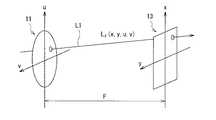
ここで、撮像素子13で受光される光について図4を参照して説明する。図4に示したように、撮像レンズ11の撮像レンズ面上において直交座標系(u,v)を、撮像素子13の撮像面上において直交座標系(x,y)をそれぞれ考え、撮像レンズ11の撮像レンズ面と撮像素子13の撮像面との距離をFとすると、図中に示したような撮像レンズ11および撮像素子13を通る光線L1は、4次元関数LF(x,y,u,v)で表されるため、光線の位置情報に加え、光線の進行方向が保持された状態で撮像素子13に記録される。すなわち、各マイクロレンズに割り当てられた複数の画素の配置によって光線の入射方向が決まっている。Here, the light received by the
このようにして撮像素子において受光がなされると、撮像素子駆動部15による駆動動作に従って、撮像素子13から撮像データが得られ、この撮像データが画像処理部14へ入力される。画像処理部14では、制御部16の制御に応じて、撮像データに対して所定の画像処理を施し、これにより撮像データDoutにより再構築画像が出力される。 When the image sensor receives light in this way, image data is obtained from the
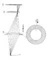
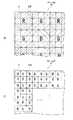
次に、この撮像装置1の特徴的な作用について、図5〜図9に示した従来の撮像装置と比較して、図10および図11を参照して説明する。なお、図5は従来の開口絞りを用いた撮像装置の概略構成を表し、図6は図5の撮像装置を用いた場合の撮像素子の受光領域、図7は図5の撮像装置で実際に取得した画像、図8および図9は従来の開口絞りを用いて各マイクロレンズに割り当てられる画素数を減らした際の受光領域を表すものである。 Next, the characteristic operation of the
図5に示したように、従来の撮像装置は、被写体2の側から、開口絞り100を有する撮像レンズ110と、マイクロレンズアレイ120と、撮像素子130とを備えており、開口絞り100は、その中央部に一つの円形の開口部100Aを有している。このため、開口絞り100Aを通過した全ての光線が、上述したように、その進行方向に関する情報を保持している。 As shown in FIG. 5, the conventional imaging apparatus includes an
従って、従来の構成では、図6に示したように、開口絞りの円形状が投影された受光領域130−1において受光がなされる。また、撮像素子130において、15×15=225個の画素Pが配置された領域に、一つのマイクロレンズが割り当てられている。また、上述したように、各マイクロレンズに割り当てられた画素Pの位置によって光線の入射方向が決定される。従って、マイクロレンズごとに、同じ位置に結像した一の画素Pの出力を抽出したのち、それらを合成する。これにより、例えば、図7に示したような、一の方向における再構築画像が取得される。この各マイクロレンズに割り当てられる画素Pが配置された領域(再構築画素領域130D)が、再構築画像の一画素分に相当する。 Therefore, in the conventional configuration, as shown in FIG. 6, light is received in the light receiving region 130-1 where the circular shape of the aperture stop is projected. In the
よって、撮像素子13上の画素数が一定である場合には、各マイクロレンズに割り当てられる画素数が少ない程、再構築画像の画素数が増え、分解能が高くなる。 Therefore, when the number of pixels on the
そこで、図8に示したように、従来の開口絞りを用いて、マイクロレンズの数を増やすことにより、各マイクロレンズに割り当てられる画素数を2×2=4つに設定した場合について考える。この場合、図9(A)に示したように、抽出画素P10では、その受光領域が扇形状となる。このとき、図9(B)に示したように、その円弧付近の領域132Aと頂角付近の領域132Bとでは、受光される光線の進行方向が異なるものとなる。このように、一つの抽出画素P10の受光領域130−1では、受光される光線の進行方向の分散が大きくなり、所望の進行方向の光線情報を得にくくなる。よって、単に各マイクロレンズに割り当てられる画素数を少なくするだけでは、抽出画素P10を合成して画像を再構築した場合、再構築画像の画素数を増やすことはできるものの、画質そのものが低下してしまう。 Therefore, as shown in FIG. 8, consider a case where the number of pixels assigned to each microlens is set to 2 × 2 = 4 by increasing the number of microlenses using a conventional aperture stop. In this case, as shown in FIG. 9A, in the extraction pixel P10, the light receiving region has a fan shape. At this time, as shown in FIG. 9B, the
これに対し、本実施の形態では、開口絞り10に4つの開口部10Aを点対称となるように設けることにより、図10に示したように、撮像素子13上には、各マイクロレンズに割り当てられる画素が配置された領域(再構築画素領域13D)に対して、この4つの開口部10Aに対応した4つの受光領域13−1が形成される。また、各マイクロレンズに割り当てられる画素Pの数を、開口部10Aの数に等しい4(2×2)つとしている。 On the other hand, in the present embodiment, four
このような構成により、図11に示したように、一つの抽出画素P1における受光領域13−1では、図9(A)および図9(B)に示した受光領域130−1に比べて、撮像素子13へ入射する光束が絞られるため、進行方向の制限された光線のみが開口部10Aを通過することとなる。よって、一つの抽出画素Pでの所望の進行方向における光線情報を取得し易くなる。 With such a configuration, as shown in FIG. 11, the light receiving region 13-1 in one extraction pixel P1 is compared with the light receiving region 130-1 shown in FIGS. 9A and 9B. Since the light beam incident on the
また、複数の開口部10Aが、開口絞り10の円周側の領域に配置されていることにより、正面方向に対してより大きな角度を有する視野での光線情報を取得することができる。 Further, since the plurality of
以上のように本実施の形態では、開口絞り10に4つの開口部10Aを設けることにより、撮像素子13に入射する光束が絞られ、各マイクロレンズに割り当てられる画素数を少なくした場合であっても、各画素Pでの所望の進行方向の光線情報を取得し易くなる。よって、画質を低下させることなく、再構築画像の画素数を増加させることができる。 As described above, in the present embodiment, the four
また、上記のような撮像装置1は、図12(A)および図12(B)に示したようなデジタルスチルカメラ3に適用することができる。なお、図12は、デジタルスチルカメラ3の概略構成を表し、(A)は正面図、(B)は側面図である。このデジタルスチルカメラ3は、筐体300の内部に撮像装置1を備えており、筐体300の上部には、シャッタ17、フラッシュ18、ファインダ光学系19などが設けられている。また、撮像装置1は、このようなカメラの他にも、位置センサや生体センサ、光学顕微鏡などに適用することが可能である。 Further, the
次に、本発明の変形例について説明する。 Next, a modified example of the present invention will be described.
(変形例1)
図13(A)および図13(B)は、本発明の変形例1に係るカラーフィルタ20,21の構成を表す平面図である。このカラーフィルタ20,21は、撮像素子13の受光面側に配置されることにより、撮像画像のカラー表示を可能にするものである。(Modification 1)
FIGS. 13A and 13B are plan views showing the configuration of the
図13(A)では、カラーフィルタ20は、マイクロレンズに対応する領域12D、すなわち2×2の画素配列ごとに色分けされた構成となっている。また、カラー配列としては、3原色のフィルタ、赤(R)、緑(G)、青(B)のフィルタの比率を1:2:1とし、緑が対角線上になるように規則的に配置された構成(配列A)を用いることができる。図13(B)では、カラーフィルタ21は、画素Pごとに色分けされた構成となっており、上記カラーフィルタ20と同じカラー配列(配列B)となっている。 In FIG. 13A, the color filter 20 is configured to be color-coded for each
このように、本発明において、所定の画素領域ごとに色分けされたカラーフィルタを配置することで、カラー表示が可能となる。この際、特に、図13(A)に示したカラーフィルタ20のように、マイクロレンズ対応領域12Dごとに色分けがなされていることにより、図13(B)とは異なり、マイクロレンズごとに同一の位置に配置された画素を抽出した場合、抽出後も同一のカラー配列とすることができる。よって、図13(B)と比べて、例えば色補間などの処理を施し易くなる。 As described above, in the present invention, color display can be performed by arranging color filters color-coded for each predetermined pixel region. At this time, in particular, as in the color filter 20 shown in FIG. 13A, the color is divided for each microlens-corresponding
(変形例2)
図14は、本発明の変形例2に係る開口絞り22の概略構成を表す平面図である。この開口絞り22は、4つの矩形の開口部22Aを有している。また、これらの開口部22Aは、開口絞り22の円周側に、点対称となるように設けられている。このように、複数の開口部の形状は、複数の開口部が互いに同一の形状であれば、開口部の形状は上記円形状に限定されず、多角形であってもよい。(Modification 2)
FIG. 14 is a plan view illustrating a schematic configuration of the
(変形例3)
図15は、本発明の変形例3に係る開口絞り23の概略構成を表す平面図である。また、この開口絞り23を用いた場合の、撮像素子の受光領域を図16、カラーフィルタの構成を図17(A)および図17(B)に示す。この開口絞り23は、8つの円形の開口部23Aを有している。また、これらの開口部23Aは、開口絞り23の円周側に、点対称となるように設けられている。これにより、図16に示したように、撮像素子13上には、各マイクロレンズに割り当てられる画素Pが配置された領域(再構築画素領域25D)に対して、この8つの開口部23Aに対応した8つの受光領域13−2が形成される。また、各マイクロレンズに割り当てられる画素Pの数を9(3×3)つとしている。(Modification 3)
FIG. 15 is a plan view illustrating a schematic configuration of the
また、カラー表示を行う場合には、図17(A)に示したように、各マイクロレンズに割り当てられる画素P、すなわち3×3の画素配列ごとに、色分けしたカラーフィルタ26を配置するか、あるいは、図17(B)に示したように、画素Pごとに色分けしたカラーフィルタ27を配置すればよい。但し、図17(A)のように、マイクロレンズに対応する領域ごとに色分けがされたカラーフィルタ26を用いることにより、図17(B)と異なり、マイクロレンズごとに画素を抽出する場合に抽出後の画像についても同一の配列とすることができるため、図17(B)に比べて、色補間などの処理を施し易くなる。 When performing color display, as shown in FIG. 17A, the
なお、開口絞り23の中央部分にもう一つ開口部23Aを設けることで、開口部23Aの数を9つとしてもよい。このように構成することで、任意の視野での光線に加え、正面方向に進行する光線を取得することができるため、正面方向における画像を再構築することができる。従って、アプリケーションによって正面での画像が必要とされる場合には、円周側に限らず、中央部分に開口部を設けるようにすることが好ましい。 The number of the
以上、実施の形態を挙げて本発明を説明したが、本発明はこれらの実施の形態に限定されるものではなく、種々の変形が可能である。例えば、上記実施の形態では、画像処理部14を、撮像装置1の構成要素の一つとして説明したが、必ずしもこの画像処理部が撮像装置の内部に設けられている必要はない。具体的には、画像処理部を、撮像装置とは別の装置、例えばPC(Personal Computer:パーソナルコンピュータ)などに設けておき、撮像装置で得られた撮像データをPCへ転送し、PCにおいて画像処理を施すようにすることも可能である。 Although the present invention has been described with reference to the embodiments, the present invention is not limited to these embodiments, and various modifications can be made. For example, in the above-described embodiment, the
また、上記実施の形態では、開口絞りの開口部の数と、各マイクロレンズに割り当てられる画素数とが同数の場合について説明したが、必ずしも同一である必要はなく、異なっていてもよい。 In the above embodiment, the case where the number of apertures of the aperture stop is the same as the number of pixels assigned to each microlens has been described, but it is not necessarily the same and may be different.
また、上記実施の形態では、開口絞りの位置を撮像レンズの被写体側(入射側)に配置した構成としているが、これに限定されず、撮像レンズの像側(出射側)あるいは、撮像レンズ内部に設けられた構成であってもよい。 In the above embodiment, the position of the aperture stop is arranged on the subject side (incident side) of the imaging lens. However, the present invention is not limited to this, and the imaging side of the imaging lens (exit side) or the inside of the imaging lens The structure provided in may be sufficient.
また、上記実施の形態では、カラーフィルタの配列を赤、緑、青が1:2:1の比率で、緑が対角線上に配置されるように配列したが、これに限定されず、他の比率や配置構成となるようにしてもよい。 In the above embodiment, the color filters are arranged such that red, green, and blue are arranged in a ratio of 1: 2: 1 and green is arranged diagonally. However, the present invention is not limited to this. You may make it become a ratio and arrangement configuration.
1…撮像装置、10…開口絞り、11…撮像レンズ、12…マイクロレンズアレイ、13…撮像素子、14…画像処理部、15…撮像素子駆動部、16…制御部、2…被写体。 DESCRIPTION OF
Claims (7)
Translated fromJapanese受光した光に基づいて撮像データを生成する撮像素子と、
前記撮像レンズ部と前記撮像素子との間で撮像レンズ部の焦点面上に配置されると共に、前記撮像素子の複数の画素に対して1つのマイクロレンズを有するマイクロレンズアレイ部とを備えた
ことを特徴とする撮像装置。An imaging lens unit having an aperture stop including a plurality of apertures;
An image sensor that generates imaging data based on the received light;
A microlens array unit disposed on a focal plane of the imaging lens unit between the imaging lens unit and the imaging device, and having one microlens for a plurality of pixels of the imaging device; An imaging apparatus characterized by the above.
ことを特徴とする請求項1記載の撮像装置。The imaging apparatus according to claim 1, further comprising an image processing unit configured to perform predetermined image processing on imaging data obtained from the imaging element.
前記抽出した画素データを合成することにより再構築画像を生成する
ことを特徴とする請求項2記載の撮像装置。The image processing unit extracts pixel data at the same position for each pixel region corresponding to each microlens from the imaging data,
The imaging device according to claim 2, wherein a reconstructed image is generated by combining the extracted pixel data.
ことを特徴とする請求項1に記載の撮像装置。The imaging apparatus according to claim 1, wherein the number of openings is equal to the number of pixels allocated to each microlens in the imaging element.
前記複数の開口部は、前記開口絞りの円周に沿って設けられている
ことを特徴とする請求項1に記載の撮像装置。The aperture stop is circular,
The imaging device according to claim 1, wherein the plurality of openings are provided along a circumference of the aperture stop.
ことを特徴とする請求項1に記載の撮像装置。The imaging device according to claim 1, wherein the plurality of openings are arranged point-symmetrically with respect to a center point of the aperture stop.
ことを特徴とする請求項1に記載の撮像装置。The image pickup apparatus according to claim 1, further comprising a color filter that is color-coded for each pixel region corresponding to each microlens on a light receiving surface side of the image pickup device.
Priority Applications (3)
| Application Number | Priority Date | Filing Date | Title |
|---|---|---|---|
| JP2007184211AJP4967873B2 (en) | 2007-07-13 | 2007-07-13 | Imaging device |
| US12/213,413US8130310B2 (en) | 2007-07-13 | 2008-06-19 | Image pickup apparatus |
| CN2008101335149ACN101345826B (en) | 2007-07-13 | 2008-07-11 | Image pickup apparatus |
Applications Claiming Priority (1)
| Application Number | Priority Date | Filing Date | Title |
|---|---|---|---|
| JP2007184211AJP4967873B2 (en) | 2007-07-13 | 2007-07-13 | Imaging device |
Publications (3)
| Publication Number | Publication Date |
|---|---|
| JP2009021919Atrue JP2009021919A (en) | 2009-01-29 |
| JP2009021919A5 JP2009021919A5 (en) | 2010-05-13 |
| JP4967873B2 JP4967873B2 (en) | 2012-07-04 |
Family
ID=40247699
Family Applications (1)
| Application Number | Title | Priority Date | Filing Date |
|---|---|---|---|
| JP2007184211AActiveJP4967873B2 (en) | 2007-07-13 | 2007-07-13 | Imaging device |
Country Status (3)
| Country | Link |
|---|---|
| US (1) | US8130310B2 (en) |
| JP (1) | JP4967873B2 (en) |
| CN (1) | CN101345826B (en) |
Cited By (9)
| Publication number | Priority date | Publication date | Assignee | Title |
|---|---|---|---|---|
| JP2010154493A (en)* | 2008-11-21 | 2010-07-08 | Sony Corp | Image pickup device |
| KR20100109408A (en)* | 2009-03-31 | 2010-10-08 | 소니 주식회사 | Solid-state imaging device, signal processing method thereof and image capturing apparatus |
| JP2010263501A (en)* | 2009-05-08 | 2010-11-18 | Sony Corp | Imaging device |
| JP2011239070A (en)* | 2010-05-07 | 2011-11-24 | Sony Corp | Solid-state image pickup device, manufacturing method for the same and electronic equipment |
| JP2014161014A (en)* | 2011-03-07 | 2014-09-04 | Panasonic Corp | Imaging apparatus and range finder |
| JP2015207815A (en)* | 2014-04-17 | 2015-11-19 | キヤノン株式会社 | Image pickup device and image pickup apparatus including image pickup device |
| JP2016006969A (en)* | 2013-01-15 | 2016-01-14 | オリンパス株式会社 | Imaging device and imaging apparatus |
| US9578235B2 (en) | 2013-10-18 | 2017-02-21 | Canon Kabushiki Kaisha | Image processing apparatus, control method, and recording medium for processing an image signal for which a focus state can be changed after image capture |
| US10051159B2 (en) | 2014-07-31 | 2018-08-14 | Panasonic Intellectual Property Management Co., Ltd. | Imaging apparatus and imaging system |
Families Citing this family (83)
| Publication number | Priority date | Publication date | Assignee | Title |
|---|---|---|---|---|
| US7834927B2 (en)* | 2001-08-22 | 2010-11-16 | Florida Atlantic University | Apparatus and method for producing video signals |
| JP4826152B2 (en)* | 2005-06-23 | 2011-11-30 | 株式会社ニコン | Image composition method and imaging apparatus |
| US10298834B2 (en) | 2006-12-01 | 2019-05-21 | Google Llc | Video refocusing |
| US8559705B2 (en) | 2006-12-01 | 2013-10-15 | Lytro, Inc. | Interactive refocusing of electronic images |
| US8019215B2 (en)* | 2007-08-06 | 2011-09-13 | Adobe Systems Incorporated | Method and apparatus for radiance capture by multiplexing in the frequency domain |
| US8244058B1 (en) | 2008-05-30 | 2012-08-14 | Adobe Systems Incorporated | Method and apparatus for managing artifacts in frequency domain processing of light-field images |
| JP5187145B2 (en)* | 2008-11-07 | 2013-04-24 | 株式会社ニコン | Image composition apparatus and method |
| US8279325B2 (en) | 2008-11-25 | 2012-10-02 | Lytro, Inc. | System and method for acquiring, editing, generating and outputting video data |
| US8289440B2 (en)* | 2008-12-08 | 2012-10-16 | Lytro, Inc. | Light field data acquisition devices, and methods of using and manufacturing same |
| US8189089B1 (en) | 2009-01-20 | 2012-05-29 | Adobe Systems Incorporated | Methods and apparatus for reducing plenoptic camera artifacts |
| US8908058B2 (en)* | 2009-04-18 | 2014-12-09 | Lytro, Inc. | Storage and transmission of pictures including multiple frames |
| JP5246424B2 (en)* | 2009-05-11 | 2013-07-24 | ソニー株式会社 | Imaging device |
| US8228417B1 (en) | 2009-07-15 | 2012-07-24 | Adobe Systems Incorporated | Focused plenoptic camera employing different apertures or filtering at different microlenses |
| US8400555B1 (en)* | 2009-12-01 | 2013-03-19 | Adobe Systems Incorporated | Focused plenoptic camera employing microlenses with different focal lengths |
| US8749620B1 (en) | 2010-02-20 | 2014-06-10 | Lytro, Inc. | 3D light field cameras, images and files, and methods of using, operating, processing and viewing same |
| US8817015B2 (en) | 2010-03-03 | 2014-08-26 | Adobe Systems Incorporated | Methods, apparatus, and computer-readable storage media for depth-based rendering of focused plenoptic camera data |
| CN103026170B (en) | 2010-08-06 | 2015-04-01 | 松下电器产业株式会社 | Imaging device and imaging method |
| JP5421207B2 (en) | 2010-08-25 | 2014-02-19 | 株式会社東芝 | Solid-state imaging device |
| US8749694B2 (en) | 2010-08-27 | 2014-06-10 | Adobe Systems Incorporated | Methods and apparatus for rendering focused plenoptic camera data using super-resolved demosaicing |
| US8803918B2 (en) | 2010-08-27 | 2014-08-12 | Adobe Systems Incorporated | Methods and apparatus for calibrating focused plenoptic camera data |
| US8724000B2 (en) | 2010-08-27 | 2014-05-13 | Adobe Systems Incorporated | Methods and apparatus for super-resolution in integral photography |
| US8665341B2 (en) | 2010-08-27 | 2014-03-04 | Adobe Systems Incorporated | Methods and apparatus for rendering output images with simulated artistic effects from focused plenoptic camera data |
| JP5254291B2 (en)* | 2010-09-07 | 2013-08-07 | 株式会社東芝 | Solid-state imaging device |
| JP5127899B2 (en) | 2010-09-14 | 2013-01-23 | 株式会社東芝 | Solid-state imaging device |
| JP5672989B2 (en)* | 2010-11-05 | 2015-02-18 | ソニー株式会社 | Imaging device |
| US8768102B1 (en) | 2011-02-09 | 2014-07-01 | Lytro, Inc. | Downsampling light field images |
| US9197798B2 (en) | 2011-03-25 | 2015-11-24 | Adobe Systems Incorporated | Thin plenoptic cameras using microspheres |
| US8717483B2 (en) | 2011-04-22 | 2014-05-06 | Panasonic Corporation | Imaging device, imaging system, and imaging method |
| WO2012143983A1 (en) | 2011-04-22 | 2012-10-26 | パナソニック株式会社 | Image capture device, imgae capture system, and image capture method |
| EP2725802A4 (en) | 2011-06-23 | 2014-07-02 | Panasonic Corp | IMAGING DEVICE |
| US9184199B2 (en) | 2011-08-01 | 2015-11-10 | Lytro, Inc. | Optical assembly including plenoptic microlens array |
| US10412367B2 (en)* | 2011-08-05 | 2019-09-10 | 3D Media Ltd | Multi-lens camera with a single image sensor |
| CN103314571B (en) | 2011-11-30 | 2017-09-29 | 松下知识产权经营株式会社 | Cameras and Camera Systems |
| CN104012076B (en)* | 2011-12-21 | 2017-11-17 | 夏普株式会社 | Imaging equipment and electronic information equipment |
| US8948545B2 (en) | 2012-02-28 | 2015-02-03 | Lytro, Inc. | Compensating for sensor saturation and microlens modulation during light-field image processing |
| US9420276B2 (en) | 2012-02-28 | 2016-08-16 | Lytro, Inc. | Calibration of light-field camera geometry via robust fitting |
| US8995785B2 (en) | 2012-02-28 | 2015-03-31 | Lytro, Inc. | Light-field processing and analysis, camera control, and user interfaces and interaction on light-field capture devices |
| US8831377B2 (en) | 2012-02-28 | 2014-09-09 | Lytro, Inc. | Compensating for variation in microlens position during light-field image processing |
| US8811769B1 (en) | 2012-02-28 | 2014-08-19 | Lytro, Inc. | Extended depth of field and variable center of perspective in light-field processing |
| JP5710835B2 (en)* | 2012-03-21 | 2015-04-30 | 富士フイルム株式会社 | Imaging device |
| CN104303493A (en) | 2012-05-09 | 2015-01-21 | 莱特洛公司 | Optimization of Optical Systems for Improved Light Field Capture and Manipulation |
| US9607424B2 (en) | 2012-06-26 | 2017-03-28 | Lytro, Inc. | Depth-assigned content for depth-enhanced pictures |
| US9858649B2 (en) | 2015-09-30 | 2018-01-02 | Lytro, Inc. | Depth-based image blurring |
| US10129524B2 (en) | 2012-06-26 | 2018-11-13 | Google Llc | Depth-assigned content for depth-enhanced virtual reality images |
| US8997021B2 (en) | 2012-11-06 | 2015-03-31 | Lytro, Inc. | Parallax and/or three-dimensional effects for thumbnail image displays |
| US9001226B1 (en) | 2012-12-04 | 2015-04-07 | Lytro, Inc. | Capturing and relighting images using multiple devices |
| US10334151B2 (en) | 2013-04-22 | 2019-06-25 | Google Llc | Phase detection autofocus using subaperture images |
| JP6286678B2 (en)* | 2013-07-12 | 2018-03-07 | パナソニックIpマネジメント株式会社 | Imaging device |
| JP2015060068A (en)* | 2013-09-18 | 2015-03-30 | 株式会社東芝 | Imaging lens and solid-state imaging device |
| CN104580869B (en)* | 2013-10-10 | 2018-06-05 | 华为技术有限公司 | A kind of light-field camera |
| EP2871830A1 (en)* | 2013-11-08 | 2015-05-13 | Thomson Licensing | Optical assembly for plenoptic camera |
| JP6548367B2 (en)* | 2014-07-16 | 2019-07-24 | キヤノン株式会社 | Image processing apparatus, imaging apparatus, image processing method and program |
| GB2544946B (en) | 2014-08-31 | 2021-03-10 | Berestka John | Systems and methods for analyzing the eye |
| US9635332B2 (en) | 2014-09-08 | 2017-04-25 | Lytro, Inc. | Saturated pixel recovery in light-field images |
| JP6598473B2 (en)* | 2015-02-27 | 2019-10-30 | キヤノン株式会社 | Imaging apparatus and image processing apparatus |
| US10275898B1 (en) | 2015-04-15 | 2019-04-30 | Google Llc | Wedge-based light-field video capture |
| US10444931B2 (en) | 2017-05-09 | 2019-10-15 | Google Llc | Vantage generation and interactive playback |
| US10540818B2 (en) | 2015-04-15 | 2020-01-21 | Google Llc | Stereo image generation and interactive playback |
| US10341632B2 (en) | 2015-04-15 | 2019-07-02 | Google Llc. | Spatial random access enabled video system with a three-dimensional viewing volume |
| US10565734B2 (en) | 2015-04-15 | 2020-02-18 | Google Llc | Video capture, processing, calibration, computational fiber artifact removal, and light-field pipeline |
| US10546424B2 (en) | 2015-04-15 | 2020-01-28 | Google Llc | Layered content delivery for virtual and augmented reality experiences |
| US10567464B2 (en) | 2015-04-15 | 2020-02-18 | Google Llc | Video compression with adaptive view-dependent lighting removal |
| US10419737B2 (en) | 2015-04-15 | 2019-09-17 | Google Llc | Data structures and delivery methods for expediting virtual reality playback |
| US10412373B2 (en) | 2015-04-15 | 2019-09-10 | Google Llc | Image capture for virtual reality displays |
| US11328446B2 (en) | 2015-04-15 | 2022-05-10 | Google Llc | Combining light-field data with active depth data for depth map generation |
| US10440407B2 (en) | 2017-05-09 | 2019-10-08 | Google Llc | Adaptive control for immersive experience delivery |
| US10469873B2 (en) | 2015-04-15 | 2019-11-05 | Google Llc | Encoding and decoding virtual reality video |
| US9979909B2 (en) | 2015-07-24 | 2018-05-22 | Lytro, Inc. | Automatic lens flare detection and correction for light-field images |
| CN106610521B (en)* | 2015-10-22 | 2019-11-19 | 中强光电股份有限公司 | Image capturing device and image capturing method |
| US10275892B2 (en) | 2016-06-09 | 2019-04-30 | Google Llc | Multi-view scene segmentation and propagation |
| CN106162113B (en)* | 2016-08-30 | 2019-03-15 | 辽宁中蓝电子科技有限公司 | Colour blackens the imaging sensor of white double-colored pixel unitary design |
| US10270947B2 (en)* | 2016-09-15 | 2019-04-23 | Microsoft Technology Licensing, Llc | Flat digital image sensor |
| US10679361B2 (en) | 2016-12-05 | 2020-06-09 | Google Llc | Multi-view rotoscope contour propagation |
| US10594945B2 (en) | 2017-04-03 | 2020-03-17 | Google Llc | Generating dolly zoom effect using light field image data |
| US10474227B2 (en) | 2017-05-09 | 2019-11-12 | Google Llc | Generation of virtual reality with 6 degrees of freedom from limited viewer data |
| US10354399B2 (en) | 2017-05-25 | 2019-07-16 | Google Llc | Multi-view back-projection to a light-field |
| US10545215B2 (en) | 2017-09-13 | 2020-01-28 | Google Llc | 4D camera tracking and optical stabilization |
| WO2019116364A1 (en)* | 2017-12-12 | 2019-06-20 | B.G. Negev Technologies And Applications Ltd., At Ben-Gurion University | Partial aperture imaging system |
| US10965862B2 (en) | 2018-01-18 | 2021-03-30 | Google Llc | Multi-camera navigation interface |
| CN108769462B (en)* | 2018-06-06 | 2020-05-05 | 北京邮电大学 | Free-view scene roaming method and device |
| JP7328025B2 (en)* | 2019-06-27 | 2023-08-16 | キヤノン株式会社 | OPTICAL DEVICE AND IMAGING SYSTEM INCLUDING THE SAME |
| CN110672883B (en)* | 2019-10-17 | 2020-10-30 | 中国科学院长春应用化学研究所 | A near-field super-resolution optical imaging method based on periodic nanohole array and lens dielectric microsphere array |
| KR20220131054A (en)* | 2021-03-19 | 2022-09-27 | 에스케이하이닉스 주식회사 | Image processing apparatus and method of operation thereof |
Citations (3)
| Publication number | Priority date | Publication date | Assignee | Title |
|---|---|---|---|---|
| JP2002320128A (en)* | 2001-04-20 | 2002-10-31 | Canon Inc | Card type camera |
| JP2005031460A (en)* | 2003-07-07 | 2005-02-03 | Canon Inc | Compound eye optical system |
| WO2006039486A2 (en)* | 2004-10-01 | 2006-04-13 | The Board Of Trustees Of The Leland Stanford Junior University | Imaging arrangements and methods therefor |
Family Cites Families (15)
| Publication number | Priority date | Publication date | Assignee | Title |
|---|---|---|---|---|
| TW262541B (en)* | 1994-05-09 | 1995-11-11 | Image Technology Internat Inc | |
| US6639629B1 (en)* | 1997-04-25 | 2003-10-28 | Konica Corporation | Camera having photographing elements for photoelectrically converting optical image into image signals |
| US6046466A (en)* | 1997-09-12 | 2000-04-04 | Nikon Corporation | Solid-state imaging device |
| JP2002529781A (en)* | 1998-11-12 | 2002-09-10 | ユーエス プレシジョン レンズ インコーポレイテッド | Color corrected projection lens using light diffraction surface |
| US6178046B1 (en)* | 1999-04-21 | 2001-01-23 | Intel Corporation | Anti-aliasing diffractive aperture and method of using same |
| JP2002124654A (en)* | 2000-10-13 | 2002-04-26 | Mitsubishi Electric Corp | Solid-state imaging device |
| JP4500434B2 (en)* | 2000-11-28 | 2010-07-14 | キヤノン株式会社 | Imaging apparatus, imaging system, and imaging method |
| JP4262446B2 (en)* | 2002-06-21 | 2009-05-13 | 富士フイルム株式会社 | Solid-state imaging device |
| JP4208232B2 (en)* | 2002-10-29 | 2009-01-14 | フジノン株式会社 | Projection-type image display apparatus having an irregular diaphragm installation structure for a projection lens and the same |
| US7405761B2 (en)* | 2003-10-01 | 2008-07-29 | Tessera North America, Inc. | Thin camera having sub-pixel resolution |
| CA2546015A1 (en)* | 2003-11-13 | 2005-06-02 | Polyfuel Inc. | Ion conductive copolymers containing one or more hydrophobic oligomers |
| US7372497B2 (en)* | 2004-04-28 | 2008-05-13 | Taiwan Semiconductor Manufacturing Company | Effective method to improve sub-micron color filter sensitivity |
| JP4826152B2 (en)* | 2005-06-23 | 2011-11-30 | 株式会社ニコン | Image composition method and imaging apparatus |
| US8243157B2 (en)* | 2006-02-07 | 2012-08-14 | The Board Of Trustees Of The Leland Stanford Junior University | Correction of optical aberrations |
| US7620309B2 (en)* | 2006-04-04 | 2009-11-17 | Adobe Systems, Incorporated | Plenoptic camera |
- 2007
- 2007-07-13JPJP2007184211Apatent/JP4967873B2/enactiveActive
- 2008
- 2008-06-19USUS12/213,413patent/US8130310B2/ennot_activeExpired - Fee Related
- 2008-07-11CNCN2008101335149Apatent/CN101345826B/ennot_activeExpired - Fee Related
Patent Citations (3)
| Publication number | Priority date | Publication date | Assignee | Title |
|---|---|---|---|---|
| JP2002320128A (en)* | 2001-04-20 | 2002-10-31 | Canon Inc | Card type camera |
| JP2005031460A (en)* | 2003-07-07 | 2005-02-03 | Canon Inc | Compound eye optical system |
| WO2006039486A2 (en)* | 2004-10-01 | 2006-04-13 | The Board Of Trustees Of The Leland Stanford Junior University | Imaging arrangements and methods therefor |
Cited By (22)
| Publication number | Priority date | Publication date | Assignee | Title |
|---|---|---|---|---|
| JP2010154493A (en)* | 2008-11-21 | 2010-07-08 | Sony Corp | Image pickup device |
| KR20100109408A (en)* | 2009-03-31 | 2010-10-08 | 소니 주식회사 | Solid-state imaging device, signal processing method thereof and image capturing apparatus |
| JP2010239337A (en)* | 2009-03-31 | 2010-10-21 | Sony Corp | Solid-state imaging device, signal processing method for solid-state imaging device, and imaging device |
| KR101696463B1 (en) | 2009-03-31 | 2017-01-23 | 소니 주식회사 | Solid-state imaging device, signal processing method thereof and image capturing apparatus |
| JP2010263501A (en)* | 2009-05-08 | 2010-11-18 | Sony Corp | Imaging device |
| US11671721B2 (en) | 2010-05-07 | 2023-06-06 | Sony Semiconductor Solutions Corporation | Solid-state imaging device, method of manufacturing solid-state imaging device, and electronic apparatus |
| US10050073B2 (en) | 2010-05-07 | 2018-08-14 | Sony Semiconductor Solutions Corporation | Solid-state imaging device, method of manufacturing solid-state imaging device, and electronic apparatus |
| US10978506B2 (en) | 2010-05-07 | 2021-04-13 | Sony Semiconductor Solutions Corporation | Solid-state imaging device, method of manufacturing solid-state imaging device, and electronic apparatus |
| US10720458B2 (en) | 2010-05-07 | 2020-07-21 | Sony Semiconductor Solutions Corporation | Solid-state imaging device, method of manufacturing solid-state imaging device, and electronic apparatus |
| US9438833B2 (en) | 2010-05-07 | 2016-09-06 | Sony Semiconductor Solutions Corporation | Solid-state imaging device, method of manufacturing solid-state imaging device, and electronic apparatus |
| US10355037B2 (en) | 2010-05-07 | 2019-07-16 | Sony Semiconductor Solutions Corporation | Solid-state imaging device, method of manufacturing solid-state imaging device, and electronic apparatus |
| JP2011239070A (en)* | 2010-05-07 | 2011-11-24 | Sony Corp | Solid-state image pickup device, manufacturing method for the same and electronic equipment |
| US10177184B2 (en) | 2010-05-07 | 2019-01-08 | Sony Semiconductor Solutions Corporation | Solid-state imaging device, method of manufacturing solid-state imaging device, and electronic apparatus |
| US9653499B2 (en) | 2010-05-07 | 2017-05-16 | Sony Semiconductor Solutions Corporation | Solid-state imaging device, method of manufacturing solid-state imaging device, and electronic apparatus |
| US9923005B2 (en) | 2010-05-07 | 2018-03-20 | Sony Corporation | Solid-state imaging device, method of manufacturing solid-state imaging device, and electronic apparatus |
| JP2014161014A (en)* | 2011-03-07 | 2014-09-04 | Panasonic Corp | Imaging apparatus and range finder |
| US9182602B2 (en) | 2011-03-07 | 2015-11-10 | Panasonic Intellectual Property Management Co., Ltd. | Image pickup device and rangefinder device |
| JPWO2014112002A1 (en)* | 2013-01-15 | 2017-01-19 | オリンパス株式会社 | Imaging device and imaging apparatus |
| JP2016006969A (en)* | 2013-01-15 | 2016-01-14 | オリンパス株式会社 | Imaging device and imaging apparatus |
| US9578235B2 (en) | 2013-10-18 | 2017-02-21 | Canon Kabushiki Kaisha | Image processing apparatus, control method, and recording medium for processing an image signal for which a focus state can be changed after image capture |
| JP2015207815A (en)* | 2014-04-17 | 2015-11-19 | キヤノン株式会社 | Image pickup device and image pickup apparatus including image pickup device |
| US10051159B2 (en) | 2014-07-31 | 2018-08-14 | Panasonic Intellectual Property Management Co., Ltd. | Imaging apparatus and imaging system |
Also Published As
| Publication number | Publication date |
|---|---|
| JP4967873B2 (en) | 2012-07-04 |
| CN101345826A (en) | 2009-01-14 |
| US8130310B2 (en) | 2012-03-06 |
| CN101345826B (en) | 2012-07-11 |
| US20090027542A1 (en) | 2009-01-29 |
Similar Documents
| Publication | Publication Date | Title |
|---|---|---|
| JP4967873B2 (en) | Imaging device | |
| JP4941332B2 (en) | Imaging device | |
| JP4483951B2 (en) | Imaging device | |
| JP5515396B2 (en) | Imaging device | |
| JP4905326B2 (en) | Imaging device | |
| JP5463718B2 (en) | Imaging device | |
| JP5672989B2 (en) | Imaging device | |
| JP4981124B2 (en) | Improved plenoptic camera | |
| US9609208B2 (en) | Image generation method, image generation apparatus, program, and storage medium | |
| JP6064040B2 (en) | Optimizing optics to improve light field capture and manipulation | |
| US9681057B2 (en) | Exposure timing manipulation in a multi-lens camera | |
| JP5067154B2 (en) | Imaging device | |
| US9826139B2 (en) | Image processing apparatus, image processing method, program, and image pickup apparatus having the image processing apparatus | |
| CN103688536B (en) | Image processing apparatus, image processing method | |
| JP2013546249A5 (en) | ||
| JP2010154493A (en) | Image pickup device | |
| JP5115068B2 (en) | Imaging device | |
| JP2015185943A (en) | Microlens with filter array and solid state image sensor | |
| JP2009290268A (en) | Imaging apparatus | |
| JP6600217B2 (en) | Image processing apparatus, image processing method, imaging apparatus, and control method thereof | |
| JP2015207815A (en) | Image pickup device and image pickup apparatus including image pickup device | |
| JP2015220600A (en) | Imaging apparatus, drive control device, control method and program |
Legal Events
| Date | Code | Title | Description |
|---|---|---|---|
| A521 | Request for written amendment filed | Free format text:JAPANESE INTERMEDIATE CODE: A523 Effective date:20100318 | |
| A621 | Written request for application examination | Free format text:JAPANESE INTERMEDIATE CODE: A621 Effective date:20100318 | |
| A977 | Report on retrieval | Free format text:JAPANESE INTERMEDIATE CODE: A971007 Effective date:20110627 | |
| A131 | Notification of reasons for refusal | Free format text:JAPANESE INTERMEDIATE CODE: A131 Effective date:20110823 | |
| A521 | Request for written amendment filed | Free format text:JAPANESE INTERMEDIATE CODE: A523 Effective date:20111014 | |
| TRDD | Decision of grant or rejection written | ||
| A01 | Written decision to grant a patent or to grant a registration (utility model) | Free format text:JAPANESE INTERMEDIATE CODE: A01 Effective date:20120306 | |
| A01 | Written decision to grant a patent or to grant a registration (utility model) | Free format text:JAPANESE INTERMEDIATE CODE: A01 | |
| A61 | First payment of annual fees (during grant procedure) | Free format text:JAPANESE INTERMEDIATE CODE: A61 Effective date:20120319 | |
| FPAY | Renewal fee payment (event date is renewal date of database) | Free format text:PAYMENT UNTIL: 20150413 Year of fee payment:3 | |
| FPAY | Renewal fee payment (event date is renewal date of database) | Free format text:PAYMENT UNTIL: 20150413 Year of fee payment:3 | |
| R250 | Receipt of annual fees | Free format text:JAPANESE INTERMEDIATE CODE: R250 | |
| R250 | Receipt of annual fees | Free format text:JAPANESE INTERMEDIATE CODE: R250 | |
| R250 | Receipt of annual fees | Free format text:JAPANESE INTERMEDIATE CODE: R250 | |
| R250 | Receipt of annual fees | Free format text:JAPANESE INTERMEDIATE CODE: R250 | |
| R250 | Receipt of annual fees | Free format text:JAPANESE INTERMEDIATE CODE: R250 |