JP2009021584A - High temperature material gate structure high temperature etching method - Google Patents
High temperature material gate structure high temperature etching methodDownload PDFInfo
- Publication number
- JP2009021584A JP2009021584AJP2008164459AJP2008164459AJP2009021584AJP 2009021584 AJP2009021584 AJP 2009021584AJP 2008164459 AJP2008164459 AJP 2008164459AJP 2008164459 AJP2008164459 AJP 2008164459AJP 2009021584 AJP2009021584 AJP 2009021584A
- Authority
- JP
- Japan
- Prior art keywords
- etching
- layer
- substrate
- chamber
- gas
- Prior art date
- Legal status (The legal status is an assumption and is not a legal conclusion. Google has not performed a legal analysis and makes no representation as to the accuracy of the status listed.)
- Pending
Links
Images


Classifications
- H—ELECTRICITY
- H01—ELECTRIC ELEMENTS
- H01L—SEMICONDUCTOR DEVICES NOT COVERED BY CLASS H10
- H01L21/00—Processes or apparatus adapted for the manufacture or treatment of semiconductor or solid state devices or of parts thereof
- H01L21/02—Manufacture or treatment of semiconductor devices or of parts thereof
- H01L21/04—Manufacture or treatment of semiconductor devices or of parts thereof the devices having potential barriers, e.g. a PN junction, depletion layer or carrier concentration layer
- H01L21/18—Manufacture or treatment of semiconductor devices or of parts thereof the devices having potential barriers, e.g. a PN junction, depletion layer or carrier concentration layer the devices having semiconductor bodies comprising elements of Group IV of the Periodic Table or AIIIBV compounds with or without impurities, e.g. doping materials
- H01L21/30—Treatment of semiconductor bodies using processes or apparatus not provided for in groups H01L21/20 - H01L21/26
- H01L21/302—Treatment of semiconductor bodies using processes or apparatus not provided for in groups H01L21/20 - H01L21/26 to change their surface-physical characteristics or shape, e.g. etching, polishing, cutting
- H01L21/306—Chemical or electrical treatment, e.g. electrolytic etching
- H01L21/3065—Plasma etching; Reactive-ion etching
- H—ELECTRICITY
- H01—ELECTRIC ELEMENTS
- H01L—SEMICONDUCTOR DEVICES NOT COVERED BY CLASS H10
- H01L21/00—Processes or apparatus adapted for the manufacture or treatment of semiconductor or solid state devices or of parts thereof
- H01L21/02—Manufacture or treatment of semiconductor devices or of parts thereof
- H01L21/04—Manufacture or treatment of semiconductor devices or of parts thereof the devices having potential barriers, e.g. a PN junction, depletion layer or carrier concentration layer
- H01L21/18—Manufacture or treatment of semiconductor devices or of parts thereof the devices having potential barriers, e.g. a PN junction, depletion layer or carrier concentration layer the devices having semiconductor bodies comprising elements of Group IV of the Periodic Table or AIIIBV compounds with or without impurities, e.g. doping materials
- H01L21/30—Treatment of semiconductor bodies using processes or apparatus not provided for in groups H01L21/20 - H01L21/26
- H01L21/31—Treatment of semiconductor bodies using processes or apparatus not provided for in groups H01L21/20 - H01L21/26 to form insulating layers thereon, e.g. for masking or by using photolithographic techniques; After treatment of these layers; Selection of materials for these layers
- H01L21/3105—After-treatment
- H01L21/311—Etching the insulating layers by chemical or physical means
- H01L21/31105—Etching inorganic layers
- H01L21/31111—Etching inorganic layers by chemical means
- H01L21/31116—Etching inorganic layers by chemical means by dry-etching
- H01L21/31122—Etching inorganic layers by chemical means by dry-etching of layers not containing Si, e.g. PZT, Al2O3
- H—ELECTRICITY
- H01—ELECTRIC ELEMENTS
- H01L—SEMICONDUCTOR DEVICES NOT COVERED BY CLASS H10
- H01L21/00—Processes or apparatus adapted for the manufacture or treatment of semiconductor or solid state devices or of parts thereof
- H01L21/02—Manufacture or treatment of semiconductor devices or of parts thereof
- H01L21/04—Manufacture or treatment of semiconductor devices or of parts thereof the devices having potential barriers, e.g. a PN junction, depletion layer or carrier concentration layer
- H01L21/18—Manufacture or treatment of semiconductor devices or of parts thereof the devices having potential barriers, e.g. a PN junction, depletion layer or carrier concentration layer the devices having semiconductor bodies comprising elements of Group IV of the Periodic Table or AIIIBV compounds with or without impurities, e.g. doping materials
- H01L21/30—Treatment of semiconductor bodies using processes or apparatus not provided for in groups H01L21/20 - H01L21/26
- H01L21/31—Treatment of semiconductor bodies using processes or apparatus not provided for in groups H01L21/20 - H01L21/26 to form insulating layers thereon, e.g. for masking or by using photolithographic techniques; After treatment of these layers; Selection of materials for these layers
- H01L21/3205—Deposition of non-insulating-, e.g. conductive- or resistive-, layers on insulating layers; After-treatment of these layers
- H01L21/321—After treatment
- H01L21/3213—Physical or chemical etching of the layers, e.g. to produce a patterned layer from a pre-deposited extensive layer
- H01L21/32133—Physical or chemical etching of the layers, e.g. to produce a patterned layer from a pre-deposited extensive layer by chemical means only
- H01L21/32135—Physical or chemical etching of the layers, e.g. to produce a patterned layer from a pre-deposited extensive layer by chemical means only by vapour etching only
- H01L21/32136—Physical or chemical etching of the layers, e.g. to produce a patterned layer from a pre-deposited extensive layer by chemical means only by vapour etching only using plasmas
- H01L21/32137—Physical or chemical etching of the layers, e.g. to produce a patterned layer from a pre-deposited extensive layer by chemical means only by vapour etching only using plasmas of silicon-containing layers
- H—ELECTRICITY
- H10—SEMICONDUCTOR DEVICES; ELECTRIC SOLID-STATE DEVICES NOT OTHERWISE PROVIDED FOR
- H10D—INORGANIC ELECTRIC SEMICONDUCTOR DEVICES
- H10D64/00—Electrodes of devices having potential barriers
- H10D64/01—Manufacture or treatment
- H10D64/031—Manufacture or treatment of data-storage electrodes
- H10D64/037—Manufacture or treatment of data-storage electrodes comprising charge-trapping insulators
Landscapes
- Engineering & Computer Science (AREA)
- Physics & Mathematics (AREA)
- Chemical & Material Sciences (AREA)
- Microelectronics & Electronic Packaging (AREA)
- Power Engineering (AREA)
- Condensed Matter Physics & Semiconductors (AREA)
- General Physics & Mathematics (AREA)
- Manufacturing & Machinery (AREA)
- Computer Hardware Design (AREA)
- General Chemical & Material Sciences (AREA)
- Chemical Kinetics & Catalysis (AREA)
- Plasma & Fusion (AREA)
- Inorganic Chemistry (AREA)
- Drying Of Semiconductors (AREA)
- ing And Chemical Polishing (AREA)
- Electrodes Of Semiconductors (AREA)
- Metal-Oxide And Bipolar Metal-Oxide Semiconductor Integrated Circuits (AREA)
- Semiconductor Memories (AREA)
- Non-Volatile Memory (AREA)
- Insulated Gate Type Field-Effect Transistor (AREA)
Abstract
Translated fromJapaneseDescription
Translated fromJapanese(発明の分野)
本発明の実施形態は、概して、高k材料の高温エッチング法に係り、特に、ゲート構造形成中における高k材料の高温エッチング法に関する。
(関連技術の説明)(Field of Invention)
Embodiments of the present invention generally relate to high-k material high temperature etching methods, and more particularly to high-k material high temperature etching methods during gate structure formation.
(Description of related technology)
半導体デバイスの次世代型超大規模集積化(VLSI)と超々大規模集積化(ULSI)にとって鍵となる技術の1つが、サブハーフミクロン以下の特徴部を信頼度高く製造することである。しかしながら、回路技術の限界に押され、VLSI及びULSI技術における相互接続部の小型化は、処理能力に更なる課題を課すこととなった。ゲートパターンを信頼性高く形成することが、VLSIとULSIの成功と個々の基板とダイの回路密度や品質の向上にあたっての継続的な取り組みに重要である。典型的には、ゲート構造はゲート誘電体層上に配置されたゲート電極を備える。ゲート構造を利用して、ゲート誘電体層の下のドレインとソース領域の間に形成されたチャネル領域における電荷キャリアの流れを制御している。 One of the key technologies for next-generation ultra-large scale integration (VLSI) and ultra-large scale integration (ULSI) of semiconductor devices is to reliably manufacture sub-half micron features. However, pushed by the limits of circuit technology, the miniaturization of interconnects in VLSI and ULSI technology has placed additional challenges on processing capabilities. Forming the gate pattern with high reliability is important for the success of VLSI and ULSI and the ongoing efforts to improve the circuit density and quality of individual substrates and dies. Typically, the gate structure comprises a gate electrode disposed on the gate dielectric layer. A gate structure is utilized to control the flow of charge carriers in the channel region formed between the drain and source regions under the gate dielectric layer.
高k誘電体(例えば、4より高い誘電率を有する材料)がゲート構造応用例においてゲート誘電体層として広く利用されている。高kゲート誘電体により低い酸化膜換算膜圧(EOT)と低いゲート漏れ電流が得られる。大抵の高k材料は周囲温度で比較的安定であるが、これらの材料はゲート構造製造過程でのエッチングが困難であることが判明している。加えて、慣用のエッチャントではゲート構造内に存在するその他の材料、例えばゲート電極及び/又はその下の材料に対しての高k材料をエッチングする際の選択性が低いため、その他の材料を覆う高k材料のインタフェース上にシリコンの窪み、フット、又はその他の関連する欠陥が残る。 High-k dielectrics (eg, materials having a dielectric constant higher than 4) are widely used as gate dielectric layers in gate structure applications. A high-k gate dielectric provides low oxide equivalent film pressure (EOT) and low gate leakage current. Most high-k materials are relatively stable at ambient temperatures, but these materials have proven difficult to etch during the gate structure fabrication process. In addition, conventional etchants cover other materials because they have low selectivity when etching high-k materials relative to other materials present in the gate structure, such as the gate electrode and / or underlying material. Silicon dimples, feet, or other related defects remain on the high-k material interface.
従って、ゲート構造の形成中に高k材料をエッチングするための改善された方法が当該分野において求められている。 Accordingly, there is a need in the art for improved methods for etching high k materials during the formation of gate structures.
ゲート構造内に配置された高k材料のエッチング方法を本発明で提供する。一実施形態において、高k材料のエッチング方法は、高k材料層をその上に有する基板をエッチングチャンバ内に設置し、少なくともハロゲン含有ガスを含むエッチングガス混合物からプラズマをエッチングチャンバ内に発生させ、プラズマの存在下で高k材料層をエッチングしながら基板温度を約100℃〜約250℃に維持することを含んでいてもよい。 A method of etching a high-k material disposed in a gate structure is provided in the present invention. In one embodiment, a method of etching a high-k material includes placing a substrate having a high-k material layer thereon in an etch chamber and generating a plasma in the etch chamber from an etch gas mixture that includes at least a halogen-containing gas. Maintaining the substrate temperature between about 100 ° C. and about 250 ° C. while etching the high-k material layer in the presence of plasma may be included.
別の実施形態においては、ゲート構造を形成するために膜積層体をエッチングする方法は、第1及び第2ポリシリコン層に挟持された高k材料を含む膜積層体をその上に有する基板をエッチングチャンバ内に設置し、基板上の第1ポリシリコン層をエッチングして高k材料が露出したトレンチを形成し、トレンチの側壁上に保護層を形成し、高k材料を保護されたトレンチを通してハロゲン含有ガスで温度約100℃〜約250℃でエッチングし、基板上に配置された第2ポリシリコン層をエッチングすることを含んでいてもよい。 In another embodiment, a method of etching a film stack to form a gate structure includes a substrate having thereon a film stack including a high-k material sandwiched between first and second polysilicon layers. Place in the etch chamber and etch the first polysilicon layer on the substrate to form a trench with exposed high-k material, form a protective layer on the sidewall of the trench, and pass the high-k material through the protected trench Etching with a halogen-containing gas at a temperature of about 100 ° C. to about 250 ° C., and etching a second polysilicon layer disposed on the substrate.
更に別の実施形態においては、ゲート構造を形成するために膜積層体をエッチングする方法は、第1及び第2ポリシリコン層に挟持された酸化ハフニウム含有層を含む膜積層体をその上に有する基板をエッチングチャンバ内に設置し、基板温度を約100℃〜約250℃に維持しながら第1ポリシリコン層、酸化ハフニウム含有層及び第2ポリシリコン層をエッチングチャンバ内で順番にエッチングすることを含んでいてもよい。 In yet another embodiment, a method for etching a film stack to form a gate structure has a film stack including a hafnium oxide-containing layer sandwiched between first and second polysilicon layers thereon. The substrate is placed in an etching chamber, and the first polysilicon layer, the hafnium oxide-containing layer, and the second polysilicon layer are sequentially etched in the etching chamber while maintaining the substrate temperature at about 100 ° C. to about 250 ° C. May be included.
更に別の実施形態においては、ゲート構造を形成するために膜積層体をエッチングする方法は、高k材料層の上に配置された金属ゲート電極をその上に有する基板をエッチングチャンバ内に設置し、金属ゲート電極層をエッチングして高k材料が露出したトレンチを形成し、高k材料をトレンチを通してハロゲン含有ガスを用いて約100℃〜約250℃でエッチングすることを含んでいてもよい。 In yet another embodiment, a method of etching a film stack to form a gate structure includes placing a substrate having a metal gate electrode disposed on a high-k material layer thereon in an etching chamber. Etching the metal gate electrode layer to form a trench with exposed high-k material, and etching the high-k material through the trench with a halogen-containing gas at about 100 ° C. to about 250 ° C.
一実施形態においては、基板上の高k材料をエッチングする方法は、その上に高k材料層を有する基板をエッチングチャンバ内に設置し、少なくともハロゲン含有ガスを含むエッチングガス混合物からプラズマをエッチングチャンバ内に形成し、プラズマの存在下で高k材料層をエッチングしながらエッチングチャンバの内側温度を約100℃を越えて維持し、プラズマの存在下で高k材料層をエッチングしながら基板温度を約100℃〜約250℃の間に維持することを含んでいてもよい。 In one embodiment, a method of etching a high-k material on a substrate includes placing a substrate having a high-k material layer thereon in an etching chamber and etching plasma from an etching gas mixture comprising at least a halogen-containing gas. The inner temperature of the etching chamber is maintained above about 100 ° C. while etching the high-k material layer in the presence of the plasma, and the substrate temperature is controlled while etching the high-k material layer in the presence of the plasma. Maintaining between 100 ° C. and about 250 ° C. may be included.
本発明は、概して、ゲート構造形成に適した膜積層体の一部である高k材料をエッチングするための方法に関する。一実施形態において、ゲート構造膜積層体の高k材料は温度約100℃〜約250℃でエッチングされる。別の実施形態において、高k材料と隣接するゲート電極層は共に約100℃〜約250℃の同様の温度でエッチングされる。本願に記載の処理は、サブミクロンの限界寸法を有する高k材料含有ゲート構造用途に有利に適している。又、この処理により、形成されるゲート構造の滑らかで垂直な、フットやシリコン窪みのない直線的なプロファイルが保たれる。エッチング処理は、単一のエッチングチャンバ内で順次実行してもよい。 The present invention generally relates to a method for etching high-k materials that are part of a film stack suitable for gate structure formation. In one embodiment, the high-k material of the gate structure film stack is etched at a temperature of about 100 ° C. to about 250 ° C. In another embodiment, both the high-k material and the adjacent gate electrode layer are etched at a similar temperature between about 100 degrees Celsius and about 250 degrees Celsius. The process described herein is advantageously suitable for high-k material containing gate structure applications having sub-micron critical dimensions. This process also maintains a smooth, vertical profile of the gate structure that is formed, free of foot and silicon depressions. The etching process may be performed sequentially in a single etching chamber.
本願に記載のエッチング処理はいずれの適切なプラズマエッチングチャンバ内で実行してもよく、例えば分離プラズマ供給源(DPS)、DPS−II、DPS−IIアドバントエッジHT、DPSプラス、又はDPS DT、HART、HART TSエッチリアクタが挙げられ、全てカリフォルニア州サンタクララのアプライドマテリアル社から入手可能である。本発明をその他の製造業者から入手可能な適切なプラズマエッチリアクタで実施してもよい。 The etching process described herein may be performed in any suitable plasma etching chamber, such as a separate plasma source (DPS), DPS-II, DPS-II Advantage Edge HT, DPS Plus, or DPS DT, HART, HART TS etch reactors, all available from Applied Materials, Inc., Santa Clara, California. The present invention may be practiced in any suitable plasma etch reactor available from other manufacturers.
図1は本発明の少なくとも1つの実施形態の実施に適した例示を目的としたエッチング処理チャンバ100の一実施形態の概略図である。チャンバ100は蓋部120を支持する導電性チャンバ壁部130を含む。壁部130は電気アース134に接続されている。蓋部120により処理チャンバ100の内部容量の上限を定める平坦な天井部、ドーム型天井部又はその他の形状の天井部が構成される。 FIG. 1 is a schematic diagram of one embodiment of an
少なくとも1つの誘導コイルアンテナセグメント112が、高周波(RF)ソース118へと整合回路119を介して連結されている。アンテナセグメント112は蓋部120の外側に位置されており、処理ガスから形成されたプラズマ155をチャンバ内に維持するために利用される。一実施形態において、誘導コイルアンテナ112に印加されるソースRF電力は約0ワットから約2500ワットの範囲にあり、周波数は約50kHz〜約13.56MHzである。別の実施形態において、誘導コイルアンテナ112に印加されるソースRF電力は約200ワットから約2000ワットの範囲にあり、例えば800ワットである。 At least one induction
蓋部120は処理中に蓋部120の内側表面162の温度を制御するのに適した1つ以上の温度制御素子を含んでいてもよい。一実施形態において、温度制御素子はその内部を流体が流れるように構成された1つ以上の導管164を含む。導管164内を循環する流体の温度は、既定の温度を維持する必要性に応じて、蓋部120を選択的に加熱又は冷却することで蓋部120の内側表面162の温度を制御する形で調節することができる。或いは、制御素子は抵抗ヒータ、ランプ及び/又は冷却装置であってもよい。 The
処理チャンバ100は基板支持台座部116(バイアス印加素子)も含み、台座部は、通常、RF信号を生成し、周波数約13.56MHzで約1500ワット以下(例えば、バイアス電力ゼロ)のバイアス電力を発生可能な第2(バイアス印加)RFソース122に連結されている。バイアス印加ソース122は基板支持台座部116に整合回路123を介して連結されている。基板支持台座部116に印加されるバイアス電力はDC又はRFであってもよい。 The
稼働中、基板114を基板支持台座部116上に載置し、静電チャック、真空、又は機械的な固締といった慣用の技法を用いてその上に保持する。ガス状成分はガスパネル138から処理チャンバ100へと供給口を通して供給され、ガス状混合物150を生成する。プラズマ155はガス状混合物150から生成される。一実施形態において、供給口は処理チャンバ100の蓋部120内に位置されたノズル170内に納められている。ノズル170は基板114の中央に向かって下方向に第1ガス状成分を供給するための少なくとも第1排出口と、処理チャンバ100の壁部130に向かって半径方向外側に第2ガス状成分を供給するための少なくとも第2排出口174を含む。このようにして、ガス混合物の第1及び第2ガス状成分の分散は、基板の中央と縁部との間で半径方向に制御することができる。混合物150から生成されるプラズマは、RF電力をRFソース118と122からそれぞれアンテナ112と基板支持台座部116に印加することで処理チャンバ100内で維持される。エッチングチャンバ100内部の圧力は、チャンバ100と真空ポンプ136との間に据えられた絞り弁127を用いて制御する。チャンバ壁部130の表面温度は、チャンバ100の壁部130内に位置された液体含有導管(図示せず)を用いて制御される。 In operation, the
基板114の温度は、支持台座部116の温度を安定させ、導管149を通して熱伝導ガスを供給源148から基板114の背面と台座部表面上の溝部(図示せず)との間に画成された流路に流すことで制御する。熱伝導ガスとしてヘリウムガスを用いて基板支持台座部116と基板114との間の熱伝導を促進してもよい。エッチング処理中、基板114を基板支持台座部116内に取り付けられた抵抗ヒータ125によって、DC電源124を介して定常状態温度まで加熱する。台座部116と基板114との間に供給されるヘリウムにより、基板114の均一な加熱が促進される。蓋部120と基板支持台座部116の双方の温度を制御することで、基板114の温度を約100℃〜約500℃に維持することができる。 The temperature of the
その他の形態のエッチングチャンバも本発明の実施に使用できることは、当業者なら理解できる。例えば、遠隔プラズマ供給源を備えたチャンバ、マイクロ波プラズマチャンバ、電子サイクロトロン共鳴(ECR)プラズマチャンバ等を利用して本発明を実行してもよい。 Those skilled in the art will appreciate that other forms of etching chambers can be used to practice the present invention. For example, the present invention may be implemented using a chamber with a remote plasma source, a microwave plasma chamber, an electron cyclotron resonance (ECR) plasma chamber, and the like.
中央演算処理装置(CPU)144、メモリ142、及びCPU144用のサポート回路146を含む制御装置140はDPSエッチング処理チャンバ100の各種コンポーネントに連結されており、エッチング処理の制御を円滑に行う。上述したようなチャンバの制御を促進するために、CPU144は様々なチャンバ及びサブプロセッサを制御するための、工業環境で使用可能ないずれの形態の汎用コンピュータプロセッサの1つであってもよい。メモリ142はCPU144に連結されている。メモリ142つまりコンピュータ可読性媒体は1つ以上の容易に入手可能なメモリ、例えばランダムアクセスメモリ(RAM)、読み出し専用メモリ(ROM)、フロッピー(商標名)ディスク、ハードディスク、又はその他のいずれの形式のローカル又はリモートデジタルストレージであってもよい。サポート回路146はCPU144に連結され、慣用のやり方でプロセッサをサポートする。これらの回路はキャッシュ、電力供給源、クロック回路、入力/出力回路、サブシステム等を含む。本願に記載されるようなエッチング処理は、通常、ソフトウェアルーチンとしてメモリ142に記憶される。ソフトウェアルーチンは、CPU144により制御されているハードウェアとは離れて設置された第2CPU(図示せず)に記憶させても及び/又は実行させてもよい。 A
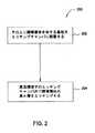
図2は図示のチャンバ100又は別の適した処理チャンバで実行することができるエッチング処理200の一実施形態のフロー図である。処理200は基板114を図1に図示されるような例示的な処理チャンバ100等のエッチング処理チャンバへと搬送する(例えば、設置する)ブロック202から開始される。基板114は高k材料誘電体層を含む膜積層体をその上に有する。一実施形態において、高k材料層は二酸化ハフニウム(HfO2)、二酸化ジルコニウム(ZrO2)、ハフニウムシリケート酸化物(HfSiO4)、ハフニウムアルミニウム酸化物(HfAlO)、ジルコニウムシリケート酸化物(ZrSiO4)、二酸化タンタル(TaO2)、酸化アルミニウム、アルミニウムドープ二酸化ハフニウム、ビスマスストロンチウムチタン(BST)、又はプラチナジルコニウムチタン(PZT)その他の少なくとも1つである。高k材料誘電体層114の一部がパターン形成されたマスク層を通して露出する。基板114は半導体基板、シリコンウェハ、ガラス基板等のいずれであってもよい。 FIG. 2 is a flow diagram of one embodiment of an
ブロック204で、露出した高k材料層を、パターン形成されたマスク層によって画成された開口部を通して高温環境内でプラズマエッチングする。高k材料層は、膜積層体のその下の層の上面が露出するまでエッチングされる。高k材料層は高温環境内でエッチングする。具体的には、チャンバコンポーネントの少なくとも一部を、高k材料層のエッチング中、約100℃より高い温度に維持する。室温で実行する慣用の高kエッチング処理中、エッチング中に発生するエッチングした高k材料の副生成物は、チャンバから排出される揮発性ガスとならず、比較的低温のチャンバ表面上で凝結する傾向がある。一実施形態においては、エッチング中、蓋部120の温度を約100℃〜約250℃に維持するため、絶縁性の高kエッチング副生成物が蓋部120上で凝結してエッチング処理の推進に使用するプラズマへの電力の結合を阻害することがない。従って、蓋部120を実質的に清浄な状態に維持することで、より均一で正確なプラズマ制御が達成され、より予測し易い、均一で正確なエッチング性能が得られる。 At
加えて、エッチング中の高k材料層の温度は、約80℃より高い温度で維持される。一実施形態において、高k材料層の温度は加熱した基板支持体を用いることで約100℃〜約250℃、例えば約130℃〜約220℃、例えば約150℃に維持される。上述したように、エッチング温度を温度約100℃〜約250℃に制御することで、高kエッチング副生成物を揮発性生成物として容易に生成し、チャンバから排出、除去することができ、より正確なプロファイルとパターン転写を行うことができる。揮発性生成物の生成により、チャンバからの残留物の排出も促進され、基板114上のエッチング後の表面が清浄となる。更に、高k材料層のエッチング用に制御した基板温度は実質的に慣用の技法のものより高いため、妥当な高k材料エッチング速度を維持するためのバイアス電力は必要なく、これによりその下の層及び/又は基板に不要な窪みを形成したり表面の損傷を招く可能性のあるイオン衝突を回避することができる。 In addition, the temperature of the high-k material layer during etching is maintained at a temperature greater than about 80 ° C. In one embodiment, the temperature of the high-k material layer is maintained at about 100 ° C. to about 250 ° C., such as about 130 ° C. to about 220 ° C., such as about 150 ° C., using a heated substrate support. As described above, by controlling the etching temperature to a temperature of about 100 ° C. to about 250 ° C., a high-k etching by-product can be easily generated as a volatile product, and discharged and removed from the chamber. Accurate profile and pattern transfer can be performed. Generation of volatile products also facilitates the discharge of residues from the chamber and cleans the etched surface on the
高k材料層は処理ガス混合物から生成したプラズマの存在下でエッチングする。一実施形態において、処理ガス混合物は少なくともハロゲン含有ガスを含む。例示的な実施形態においては、ハロゲン含有ガスは塩素含有ガスであってもよい。ハロゲン含有ガスの適切な例にはBCl3、Cl2等が含まれる。ハロゲン含有ガス内のハロゲン元素が高k材料層をエッチングし、高k材料層を基板114から除去する。高k材料層がハフニウムを含有する実施形態においては、処理ガスから放出された塩素元素がハフニウム含有材料から放出されたハフニウム元素と反応し、処理チャンバから容易に排出される揮発性副生成物である塩化ハフニウムを生成する。高温での高kエッチング処理により副生成物の揮発性は上昇するため、エッチング副生成物は基板支持体及び蓋部(又はその他の高温チャンバ表面)から効率的に除去され、エッチング処理後の表面は清浄で残留物のないものとなる。The high-k material layer is etched in the presence of a plasma generated from the process gas mixture. In one embodiment, the process gas mixture includes at least a halogen-containing gas. In an exemplary embodiment, the halogen containing gas may be a chlorine containing gas. Suitable examples of halogen-containing gases include BCl3 , Cl2 and the like. The halogen element in the halogen-containing gas etches the high-k material layer and removes the high-k material layer from the
任意で、炭化水素ガスを処理ガスに供給してもよい。炭化水素ガスにより、エッチング処理中にエッチングされた高k材料層とマスク層の側面に堆積する高分子材料が得られる。これにより限界寸法とプロファイル制御が改善される。炭化水素ガスの例にはCH4、CHF3、CH2F2及びその組み合わせが含まれる。Optionally, a hydrocarbon gas may be supplied to the process gas. The hydrocarbon gas provides a polymeric material that deposits on the sides of the high-k material layer and mask layer etched during the etching process. This improves critical dimension and profile control. Examples of hydrocarbon gases include CH4 , CHF3 , CH2 F2 and combinations thereof.
幾つかの処理パラメータは、高k材料層のエッチング中に調節してもよい。一実施形態においては、高kエッチング処理ガスの存在下でのチャンバ圧は約2mTorr〜約500mTorr、例えば約20mTorrに調節される。RFソース電力を印加して、高kエッチング処理ガスから生成したプラズマを維持してもよい。例えば、約0ワット〜約1500ワットの電力を誘導結合アンテナソースに印加して、プラズマをエッチングチャンバ内部で維持してもよい。RFバイアス電力は約0ワット〜約1000ワット、例えば約250ワットで印加してもよい。一実施形態においては、バイアス電力を使用しないことからイオンの衝突が軽減され、ゲート下のシリコンソースとドレインに望ましくない窪みが発生するのが大幅に抑制される。或いは、バイアス電力を必要に応じて排除してもよい。高kエッチング処理ガスはチャンバへと流量約0sccm〜約500sccmで流すことができる。例えば、ハロゲン含有ガスを流量約5sccm〜約500sccm、例えば約30sccm〜約100sccmで供給してもよい。炭化水素ガスは流量約0sccm〜約100sccm、例えば約0sccm〜約10sccmで供給してもよい。不活性ガスを流量約0sccm〜約500sccmで供給してもよい。基板温度は約80℃より高く、例えば約120℃より高く、例えば約150℃に維持する。 Some processing parameters may be adjusted during the etching of the high-k material layer. In one embodiment, the chamber pressure in the presence of a high-k etch process gas is adjusted to about 2 mTorr to about 500 mTorr, such as about 20 mTorr. RF source power may be applied to maintain the plasma generated from the high-k etch process gas. For example, about 0 watts to about 1500 watts of power may be applied to the inductively coupled antenna source to maintain the plasma inside the etch chamber. The RF bias power may be applied from about 0 watts to about 1000 watts, such as about 250 watts. In one embodiment, since no bias power is used, ion bombardment is mitigated, and undesirable depressions in the silicon source and drain under the gate are greatly suppressed. Alternatively, the bias power may be eliminated as necessary. The high-k etch process gas can be flowed into the chamber at a flow rate between about 0 sccm and about 500 sccm. For example, the halogen-containing gas may be supplied at a flow rate between about 5 sccm and about 500 sccm, such as between about 30 sccm and about 100 sccm. The hydrocarbon gas may be supplied at a flow rate between about 0 sccm and about 100 sccm, such as between about 0 sccm and about 10 sccm. The inert gas may be supplied at a flow rate between about 0 sccm and about 500 sccm. The substrate temperature is higher than about 80 ° C., for example, higher than about 120 ° C., for example, maintained at about 150 ° C.
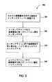
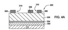
図3は図示のチャンバ100又はその他の適した処理チャンバで実行し得るエッチング処理250の一実施形態のフロー図である。図4A−4Dは処理250の各段階に対応する複合基板の一部の概略断面図である。処理250は図4A−4Dにおけるゲート構造の形成を説明するものであるが、処理250はその他の構造の形成にも有益に利用できる。 FIG. 3 is a flow diagram of one embodiment of an
処理250は基板114をエッチング処理チャンバ、例えば図1に図示されるような例示としての処理チャンバ100に搬送する(つまり設置する)ブロック252から開始される。図4Aに図示の実施形態においては、基板114はゲート構造の製造に適した高k材料の誘電体層304を含む膜積層体300をその上に有している。基板114は半導体基板、シリコンウェハ、ガラス基板等のいずれであってもよい。膜積層体300を構成している複数の層は1つ以上の適した慣用の堆積法、例えば原子層蒸着(ALD)、物理気相蒸着(PVD)、化学気相蒸着(CVD)、プラズマCVD(PECVD)等を用いて形成することができる。
一実施形態において、膜積層体300は高k誘電体層304(高k材料は4.0より高い誘電率を有している)を挟持している少なくとも1つ以上の層302、306を含む。膜積層体300は誘電体層(図示せず)上に、又は基板114上に直接的に配置してもよい。誘電体層の適切な例には酸化物層、窒化物層、窒化チタン層、酸化物と窒化物層の複合体、窒化物層を挟持する少なくとも1つ以上の酸化物層、及びその組み合わせその他が含まれるが、これに限定されるものではない。パターン形成されたマスク308、例えばハードマスク、フォトレジストマスク、又はその組み合わせを開口部310を介して膜積層体300の一部を露出し、その上に特徴部をエッチングするためのエッチングマスクとして使用してもよい。 In one embodiment, the
図4Aに図示の実施形態において、高k材料層304は二酸化ハフニウム(HfO2)、二酸化ジルコニウム(ZrO2)、ハフニウムシリケート酸化物(HfSiO4)、ハフニウムアルミニウム酸化物(HfAlO)、ジルコニウムシリケート酸化物(ZrSiO4)、二酸化タンタル(TaO2)、酸化アルミニウム、アルミニウムドープ二酸化ハフニウム、ビスマスストロンチウムチタン(BST)、又はプラチナジルコニウムチタン(PZT)、その他の層であってもよい。例示的な実施形態において、高k材料はハフニウムアルミニウム酸化物(HfAlO)である。高k材料層304の厚さは約10Å〜約500Å、例えば約50Å〜約300Å、例えば約150Åである。In the embodiment illustrated in FIG. 4A, the high-
第1層306は高k材料層304上に配置され、1つ以上の層を含む場合がある。一実施形態において、第1層306はゲート構造でゲート電極層として利用されるポリシリコン層である。或いは、第1層306はゲート電極に利用する金属材料であってもよい。金属ゲート電極の例にはタングステン(W)、ケイ化タングステン(WSi)、タングステンポリシリコン(W/ポリ)、タングステン合金、タンタル(Ta)、窒化タンタル(TaN)、窒化タンタルケイ素(TaSiN)、及び窒化チタン(TiN)その他が含まれる。更に別の実施形態において、ゲート電極層306は金属材料の上に配置されたポリシリコン層を含む複合膜であってもよい。この特定の実施形態において、ゲート電極層306は窒化チタン(TiN)層上に配置されたポリシリコン層であってもよい。図4Aに図示の実施形態において、高k材料層304上に配置された第1層306はポリシリコン層である。第1層306の厚さは約500Å〜約4000Å、例えば約800Å〜約2500Å、例えば約1650Åである。 The
第2層302は高k材料層304の下に配置されており、この層もまた1つ以上の層を含んでいてもよい。一実施形態において、第2層302は誘電体層、例えばポリシリコン層、酸化ケイ素層、窒化ケイ素層、酸窒化ケイ素層又はその組み合わせであってもよい。第2層302が存在しない一部の実施形態においては、膜積層体300の高k材料層304を基板114上に直接的に堆積してもよい。図4Aに図示の実施形態において、第2層302はポリシリコン層であり、厚さは約50Å〜約2000Å、例えば約100Å〜約1000Å、例えば約500Åである。 The
ブロック254でエッチング処理を実行し、図4Bに図示されるように、パターンが形成されたマスク308によって画成された開口部310を通して基板114上の第1層306をエッチングして、第1層306にトレンチ320を形成する。ブロック254で実行するエッチング処理は第1層306の異なる部位をエッチングするための1つ以上のエッチング工程を有していてもよい。一実施形態において、エッチング処理は単一工程のエッチング処理、つまり高k材料層304が露出するまで第1層306を一工程でエッチングするものであってもよい。別の実施形態において、エッチング処理は基板114上の第1層306の異なる部位をエッチングするための複数の工程を含むものであってもよい。 An etching process is performed at
例示的な実施形態においては、複数のエッチング工程を実行して第1層306をエッチングし、膜積層体300の高k材料層304を露出させる。ブレイクスルーエッチングをまず最初に行って、第1層306の上面、例えば自然酸化物部位をエッチングしてもよい。ブレイクスルーエッチング用のエッチングガス混合物はフッ化炭素ガスを含む。ガス混合物から生成したプラズマから発生した反応性種は酸化ケイ素等の自然酸化物と反応し、SiF4及びCO2等の揮発性反応生成物を生成し、これらは処理チャンバから排出される。ブレイクスルーエッチング用のエッチングガス混合物の適切な例にはCF4、CHF3、CH2F2、CH3F、C4F8等が含まれる。任意で、不活性ガスをエッチングガス混合物と共に供給してもよい。適切な不活性ガスの例にはAr、He、Kr、Ne等が含まれる。In the exemplary embodiment, multiple etching steps are performed to etch the
ブレイクスルーエッチング中のエッチングガス混合物存在下のチャンバ圧は調節される。ある例示的な実施形態において、エッチングチャンバ内の処理圧力は約2mTorr〜約100mTorr、例えば約4mTorrに調節される。RFソース電力を印加してエッチングガス混合物から形成されたプラズマを維持してもよい。例えば、約100ワット〜約1500ワット、例えば約300ワットの電力を誘導結合アンテナソースに印加して、プラズマをエッチングチャンバ内で維持してもよい。RFバイアス電力を約100ワット〜約1500ワット、例えば約100ワットで印加してもよい。ブレイクスルーエッチング用のエッチングガス混合物はチャンバ内へと流量約50sccm〜約1000sccmで流してもよい。例えば、フッ化炭素ガスは流量約5sccm〜約500sccm、例えば100sccmで供給してもよい。不活性ガスは流量約0sccm〜約500sccmで供給してもよい。基板温度は約30℃〜約500℃で維持する。別の実施形態において、基板は約80℃より高い温度、例えば約100℃〜約250℃、例えば約130℃〜約220℃、例えば約150℃で維持する。 The chamber pressure in the presence of the etching gas mixture during breakthrough etching is adjusted. In an exemplary embodiment, the process pressure in the etch chamber is adjusted to about 2 mTorr to about 100 mTorr, such as about 4 mTorr. RF source power may be applied to maintain a plasma formed from the etching gas mixture. For example, a power of about 100 watts to about 1500 watts, such as about 300 watts, may be applied to the inductively coupled antenna source to maintain the plasma in the etching chamber. The RF bias power may be applied from about 100 watts to about 1500 watts, such as about 100 watts. The etch gas mixture for breakthrough etching may flow into the chamber at a flow rate between about 50 sccm and about 1000 sccm. For example, the fluorocarbon gas may be supplied at a flow rate between about 5 sccm and about 500 sccm, such as 100 sccm. The inert gas may be supplied at a flow rate between about 0 sccm and about 500 sccm. The substrate temperature is maintained at about 30 ° C. to about 500 ° C. In another embodiment, the substrate is maintained at a temperature greater than about 80 ° C, such as from about 100 ° C to about 250 ° C, such as from about 130 ° C to about 220 ° C, such as about 150 ° C.
自然酸化物にブレイクスルーエッチングを施した後、メインエッチングを行って第1層306の主要部位のエッチングを行う。第1層306をパターン形成されたマスク308を介してエッチングし、その下の高k材料304の上面312が露出するまで第1層306にトレンチ320を形成する。ブレイクスルーエッチングとメインエッチングは基板114をエッチングチャンバから取り出すことなく連続的に行ってもよい。メインエッチング工程用のエッチングガス混合物は少なくともハロゲン含有ガスとフッ化炭素ガスを含む。ハロゲン含有ガスの適切な例にはHBr、HCl、Cl2、Br2、NF3、その組み合わせ等が含まれる。フッ化炭素ガスの適切な例にはCF4、CHF3、CH2F2、CH3F、C4F8、その組み合わせが含まれる。任意で、キャリアガス、例えばO2、N2、その組み合わせ等及び不活性ガスをエッチングガス混合物と共に供給してもよい。不活性ガスの適切な例にはAr、He、Kr等が含まれる。特定の実施形態において、メインエッチングガス混合物にはHBrガス、NF3ガス、CF4ガス、O2ガス、N2ガス及びHeガスが含まれていてもよい。After the breakthrough etching is performed on the natural oxide, the main etching is performed and the main portion of the
一実施形態において、ブレイクスルーエッチング及びメインエッチング中に第1層306のエッチングに利用する処理パラメータは、実質的に同様のやり方で制御してもよい。別の実施形態において、ブレイクスルーエッチング及びメインエッチング中に第1層306のエッチングに利用する処理パラメータは、異なる処理要件に応じて異なっていてもよい。更に、更に別の実施形態において、第1層306のメインエッチング中の処理パラメータを必要に応じて変更し、メインエッチング処理を2つ以上の工程からなるエッチング処理としてもよい。 In one embodiment, the process parameters utilized for etching the
一実施形態において、メインエッチング用ガス混合物のチャンバ圧は第1層306のエッチングに調節する。ある例示的な実施形態において、エッチングチャンバ内の処理圧は約2mTorr〜約100mTorr、例えば約7mTorrに調節される。RFソース電力を印加することで、エッチングガス混合物から形成したプラズマを維持してもよい。例えば、電力約100ワット〜約1500ワット、例えば約300ワットを誘導結合型アンテナソースに印加し、プラズマをエッチングチャンバ内で維持してもよい。約100ワット〜約1000ワット、例えば約150ワット〜約250ワットのRFバイアス電力を印加してもよい。メインエッチング中のエッチングガス混合物はチャンバ内へと流量約50sccm〜約1000sccmで流してもよい。例えば、ハロゲン含有ガスは流量約5sccm〜約500sccm、例えば170sccmで供給してもよい。フッ化炭素ガスは流量約5sccm〜約500sccm、例えば約40sccm〜約70sccmで供給してもよい。不活性ガスは流量約0sccm〜約500sccmで供給してもよい。基板温度は約30℃〜約500℃で維持される。別の実施形態において、基板温度は約80より高く、例えば約120℃より高く、例えば約150℃で維持される。 In one embodiment, the chamber pressure of the main etching gas mixture is adjusted to etch the
図4Bに図示されるように第1層306にトレンチ320が形成された後、オーバーエッチング処理を行って、エッチングした第1層306の側壁322上に保護層を堆積するのみならず、基板114上に残留している第1層306のトポグラフィをエッチングしてもよい。露出した側壁322上に堆積された保護層により、基板114上に残留している第1層306のトポグラフィのエッチングの最中及び/又は続くエッチング処理中に側壁が攻撃されるのを防止し、これによりプロファイル制御の喪失とパターン変形を防止する。 After the
一実施形態において、ブロック254での第1層306のエッチングのメインエッチング処理で使用するガス混合物に加えて、ケイ素とハロゲンを含有したガスを添加して、基板114上に残存する第1層306のトポグラフィをエッチングしてもよい。ガス混合物への添加に適したガスの例にはSiCl4等が含まれる。ケイ素とハロゲンを含有するガスから発生したハロゲン反応性種により、エッチング残留物と残存する第1層306が基板表面から除去される。加えて、ケイ素・ハロゲン含有ガスから発生したケイ素反応性種は第1層306と反応し、エッチングした表面にケイ素側壁保護層を形成し、これにより堅固な側壁の保護が得られる。この堅固な側壁保護により、第1層306は続く高k材料層304とその下の第2層302のエッチング処理中の攻撃から保護される。In one embodiment, in addition to the gas mixture used in the main etch process of etching the
ブロック256で、高k材料層304の露出した上面312をパターン形成したマスク308とトレンチ320によって画成された開口部310を通して高温環境下でエッチングする。高k材料層304を、図4Cに図示されるように、その下の第2層302の上面314が露出するまでエッチングする。一実施形態において、高温環境は、処理チャンバ100の蓋部120の温度を約100℃〜約150℃、例えば約120℃に維持することで得られる。 At
高k材料層304のエッチングに利用する高kエッチングガス混合物としては、第1層306の側壁322を覆うケイ素保護層とその下の第2層302よりも高k材料層304に対して高い選択性を有するものを選択する。第1層306の側壁322は堅牢な保護層によって保護されているため、比較的高い処理温度、例えば慣用の技法で使用する室温処理よりも高いものを用いて高k材料層304をエッチングしてもよく、第1層306に形成されるトレンチのプロファイルに悪影響が及ぼされることはない。一実施形態において、高k材料層304は約80℃より高い温度、例えば約100℃〜約250℃、例えば約130℃〜約220℃、例えば約150℃でエッチングする。室温で行う慣用の高kエッチング処理においては、エッチング中に発生する、エッチング済みの高k材料の副生成物はチャンバから排出される揮発性反応生成物を生成せずに基板表面上に蓄積する傾向があり、これによりパターン転写が不良となる。従って、約100℃〜約250℃の間でエッチング温度を制御することで、高kエッチング副生成物を揮発性生成物として容易に生成し、チャンバから排出、除去し、より正確なプロファイルとパターン転写を得ることができる。揮発性生成物を生成することでチャンバからの残留物の排出も促進され、基板114のエッチング後の表面が清浄となる。更に、高k材料層304のエッチングに向けて制御した基板温度は実質的に慣用の技法よりも高いため、妥当な高k材料エッチング速度を維持するためにバイアス電力を必要とせず、下層及び/又は基板に不要な窪みや表面の損傷を生じる可能性のある衝突が回避できる。 As a high-k etching gas mixture used for etching the high-
一実施形態において、高k材料層304のエッチング用に供給される高kガス混合物は少なくともハロゲン含有ガスを含む。例示的な実施形態において、ハロゲン含有ガスは塩素含有ガスであってもよい。適したハロゲン含有ガスの例にはBCl3、Cl2等が含まれる。ハロゲン含有ガスに含まれるハロゲン元素が高k材料層304をエッチングし、高k材料層304を基板114から除去する。ハロゲン含有ガスがBCl3である実施形態においては、ハロゲン含有ガスにより材料304とその下の第1層306との間で高い選択性が得られる。例えば、高k材料層304がハフニウム・酸化物含有材料である実施形態の場合、エッチングプラズマ解離中にBCl3ガスから放出されるホウ素元素がハフニウム・酸化物含有材料から放出される酸素元素と反応し、BxOy保護層を基板の露出面上に形成する。エッチング処理中に形成されたBxOy保護層はケイ素表面、例えばエッチングされた上層又は先だって露出された下層を不動態化し、これにより基板上のエッチングしたくないその他の領域がエッチング中に攻撃に曝され、基板上に窪みや欠陥が生じることが防止される。BCl3ガスから放出される塩素元素はハフニウム・酸化物含有材料から放出されるハフニウム元素と反応して、チャンバから排出される塩化ハフニウム(HfCl4)揮発性副生成物を生成する。高温での高kエッチング処理により副生成物の揮発性が上昇するため、エッチング副生成物は基板から効率よく除去され、エッチング処理後、基板上にはエッチング後の清浄で残留物のない表面が残る。従って、垂直方向に真っ直ぐに延びた、欠陥のない(窪みやフットのない)構造と隣接する層に対しての高い選択性を実現可能な高kエッチング処理が得られる。In one embodiment, the high-k gas mixture supplied for etching the high-
任意で、炭化水素ガスをガス混合物に供給してもよい。炭化水素ガスにより、エッチング処理中のプラズマ解離の間に、図4Cに図示の、第1層306の側壁322とエッチングした高k材料層304の側壁324上に堆積される高分子材料が得られる。炭化水素ガスの例にはCH4、CHF3、CH2F2、及びその組み合わせが含まれる。Optionally, hydrocarbon gas may be supplied to the gas mixture. The hydrocarbon gas provides a polymeric material that is deposited on the
一実施形態においては、高k材料304を上部第1層306のエッチングに使用するものと同一のチャンバ内でエッチングし、膜積層体300のエッチングを1つのチャンバ内に統合してもよい。ブロック254及び256でのエッチング処理を、基板114を処理チャンバ100から取り出すことなく連続的に行ってもよい。第1層306のエッチング用に選択する温度を、高k材料304のエッチング用に構成した温度と実質的に同じに制御し、基板温度の変更、安定化のために待機することなく基板114を効率的にエッチングしてもよい。一実施形態において、ブロック256での高k材料エッチング処理とブロック254での第1層306のエッチングの双方を80℃より高い温度、例えば約100℃〜約200℃の同様の温度で行ってもよい。一実施形態において、第1層306と高k材料304の双方のエッチング用の温度は約80℃より高く、例えば約100℃〜約250℃、例えば約130℃〜約220℃、例えば約150℃に制御する。 In one embodiment, the high-
高k材料層304をエッチングしながら、幾つかの処理パラメータを調節してもよい。ブロック254で調節した処理パラメータを、ブロック256で調節した処理パラメータへと円滑に移行させてもよい。一実施形態において、高kエッチングガス混合物の存在下でのチャンバ圧は約2mTorr〜約500mTorr、例えば約20mTorrに調節される。RFソース電力を印加して、高kエッチングガス混合物から生成したプラズマを維持してもよい。例えば、約0ワット〜約1500ワットの電力を誘導結合アンテナソースに印加して、エッチングチャンバ内でプラズマを維持してもよい。RFバイアス電力を約0ワット〜約1000ワット、例えば約250ワットで印加してもよい。一実施形態においては、バイアス電力を使用しないことからイオンの衝突が軽減され、ゲート下のシリコンソースとドレインに望ましくない窪みが発生するのが大幅に抑制される。或いは、必要に応じてバイアス電力を排除してもよい。高kエッチングガス混合物をチャンバへと流量0sccm〜約500sccmで流してもよい。例えば、ハロゲン含有ガスを流量約5sccm〜約500sccm、例えば約30sccm〜約100sccmで供給してもよい。炭化水素ガスは流量約0sccm〜約100sccm、例えば約0sccm〜約10sccmで供給してもよい。不活性ガスを流量約0sccm〜約500sccmで供給してもよい。基板温度は約80℃より高く、例えば約120℃より高く、例えば約150℃に維持する。 While etching the high-
任意で、酸素ガスフラッシュ処理を、ブロック256での高kガス混合物のエッチングチャンバ内への供給に先立って行ってもよい。酸素ガスフラッシュ処理は、第1層306のエッチング後の側壁322上への酸化層の形成を補佐することで、エッチングした表面上に表面不動態層を設ける。第1層306はケイ素含有材料であるため、チャンバに供給された酸素ガスは第1層306のケイ素元素と反応し、側壁にケイ素酸化物保護層が形成される。酸素ガスフラッシュ処理で使用する処理パラメータは調節する。一実施形態において、チャンバ圧は約2mTorr〜約500mTorr、例えば約20mTorrで調節される。約200ワットから約2000ワットのRFソース電力を誘導結合アンテナソースに印加して、エッチングチャンバ内でプラズマを維持してもよい。酸素ガスは流量約20sccm〜約500sccm、例えば約50sccm〜約150sccmで供給してもよい。或いは、He又はAr等の不活性ガスを流量約0sccm〜約500sccmで供給してもよい。基板温度は約80℃より高い温度、例えば約100℃〜約250℃、例えば約130℃〜約220℃、例えば約150℃で維持する。 Optionally, an oxygen gas flush process may be performed prior to supplying the high-k gas mixture into the etch chamber at
ブロック258で、パターン形成されたマスク308とトレンチ320によって画成された開口部310を通して膜積層体300の第2層302をエッチングする。図4Dに図示されるように、エッチング処理により、基板114の上面316が露出するまで第2層302をエッチングする。ブロック258で実行するエッチング処理は、第1層306をエッチングするためのブロック254で実行するエッチング処理と同様に、第2層302の異なる部位をエッチングするための1つ以上のエッチング工程を有していてもよい。一実施形態において、エッチング処理は単一の工程からなるエッチング処理、つまり下の基板114の上面316が露出するまで第2層302をエッチングするものであってもよい。別の実施形態において、エッチング処理は基板114上の第2層302の異なる部位をエッチングするための複数の工程を含んでいてもよい。 At
例示的な実施形態においてはブロック258で2工程エッチング処理を行って、膜積層体300の第2層306をエッチングしてもよい。第一に、ブレイクスルーエッチングをまず最初に行って、第2層302の表面へとエッチングを施す。ブレイクスルーエッチング用のエッチングガス混合物はフッ化炭素ガスを含む。ブロック258での第2層302のブレイクスルーに用いるブレイクスルーガス混合物は、上述したようなブロック254での第1層306のブレイクスルーに用いたブレイクスルーガス混合物と実質的に同じであってもよい。任意で、不活性ガスをエッチングガス混合物と共に供給してもよい。適切な不活性ガスの例にはAr、He、Kr、Ne等が含まれる。 In an exemplary embodiment, a second step etch process may be performed at
ブレイクスルーエッチングを施した後、メインエッチングを行ってマスク開口部310を通して露出した第2層306の残留部位のエッチングを行う。ブレイクスルーエッチングとメインエッチングは基板114をエッチングチャンバから取り出すことなく連続的に行ってもよい。第1及び第2層306、302の双方がポリシリコン層である実施形態においては、第1及び第2層306、302の主要部位のエッチングに使用するガス混合物と処理パラメータは実質的に同じであってもよい。メインエッチング用のエッチングガス混合物は少なくともハロゲン含有ガスとフッ化炭素ガスを含む。ハロゲン含有ガスの適切な例にはHBr、HCl、Cl2、Br2、NF3、その組み合わせ等が含まれる。適したフッ化炭素ガスの例にはCF4、CHF3、CH2F2、CH3F、C4F8、その組み合わせ等が含まれる。任意で、キャリアガス、例えばO2、N2、N2O、NO2、その組み合わせ等及び不活性ガスをエッチングガス混合物と共に供給してもよい。不活性ガスの適切な例にはAr、He、Kr、Ne等が含まれる。一実施形態において、メインエッチング工程用のエッチングガス混合物にはHBrガス、NF3ガス、CF4ガス、O2ガス、N2ガス及びHeガスが含まれていてもよい。ブロック258で調節する処理パラメータはブロック254について記載したものと実質的に同様に制御してもよい。After performing breakthrough etching, main etching is performed to etch the remaining portion of the
膜積層体300の第2層302を上部第1層306と高k材料304のエッチングに用いたチャンバと同一のチャンバでエッチングし、膜積層体300のエッチングを単一のチャンバに統合してもよい。第1層306、高k材料304及び第2層302は同様の温度でエッチングされることから、基板の温度を各層のエッチング処理に用いる安定した処理温度にする際に必要な時間が短縮され、スループットが向上する。 Even if the
その他の高kエッチング処理を高温環境での高k材料層のエッチングで利用するよう適合させることも考えられる(例えば、蓋部120等のチャンバ表面を約100℃より高い温度に維持する)。これに限定するものではないが、2006年3月21日出願の米国特許出願第11/386054号、2007年7月12日出願の米国特許出願第11/777259号、2007年4月17日出願の米国特許出願第11/736562号、2007年7月6日出願の米国特許仮出願第60/948376号、及び2002年3月6日出願の米国特許第6806095号に記載の高kエッチング処理に変更を加えて、上述したようなチャンバ表面温度の調節による高温エッチング環境の実現を含めてもよい。 It is contemplated that other high-k etch processes may be adapted for use in etching high-k material layers in high temperature environments (eg, maintaining chamber surfaces such as
図5A−Cは上述の高kエッチング処理を用いて有益にエッチングし得る異なる膜積層体に対応する複合基板の一部の概略断面図である。例えば、図5Aは高k誘電体層504を有する膜積層体510を図示している。高k誘電体層504はハフニウム含有材料、例えばHf2O、HfSiO、HfSiN等である。高k誘電体層504と基板114との間には高モビリティインタフェース層502が配置されている。高モビリティインタフェース層502は通常、薄いSiON層である。高モビリティインタフェース層502のSiON材料は、層502の化学量論がHfとSiONの混合により積層体全体として最終的により高いkが得られることを含み得ることでランク付けすることができる。適したインタフェース層の例は、2003年4月4日出願の米国特許出願第10/407930号に記載されている。金属ゲート層512は高k誘電体層504上に配置されている。低抵抗層514は金属ゲート層512上に配置されている。 5A-C are schematic cross-sectional views of portions of a composite substrate corresponding to different film stacks that can be beneficially etched using the high-k etch process described above. For example, FIG. 5A illustrates a
別の実施形態において、図5Bは高k誘電体層504を有する膜積層体530を示している。高モビリティインタフェース層502は高k誘電体層504と基板114との間に配置されている。薄い誘電性キャップ層532が高k誘電体層504の上に配置されている。金属ゲート層534が誘電性キャップ層532上に配置されている。低抵抗層536、例えばポリシリコンが金属ゲート層534上に配置されている。 In another embodiment, FIG. 5B shows a
別の実施形態において、図5CはTANOS構造体等の電荷トラップ型のフラッシュメモリデバイスに適した膜積層体550を図示している。膜積層体550は基板114上に配置されたトンネル酸化物層552を含む。電荷トラップ型窒化物層554はトンネル酸化物層552上に配置されている。高k誘電体層504は電荷トラップ型窒化物層554上に配置されている。高WP金属層556は高k誘電体層504上に配置されている。低抵抗層558、例えばPVD金属層は高WP金属層556上に配置される。 In another embodiment, FIG. 5C illustrates a
従って、本発明により高温エッチング処理によって高k材料層をエッチングするための改善された方法が得られる。高温エッチング処理により、高k材料がパターン転写の損失なく効率的にエッチングされるため、欠陥のない、エッチング後の表面が清浄な、望ましいプロファイルと寸法の構造が形成され、有利である。 Thus, the present invention provides an improved method for etching high k material layers by high temperature etching processes. The high temperature etching process advantageously etches high-k materials without loss of pattern transfer, which results in the formation of a desired profile and dimension structure that is defect-free and has a clean post-etch surface.
上記記載は本発明の実施形態を対象としているが、本発明の基本的な範囲から逸脱することなく本発明のその他及び更なる実施形態を創作することができ、本発明の範囲は特許請求の範囲に基づいて定められる。 While the above description is directed to embodiments of the invention, other and further embodiments of the invention may be created without departing from the basic scope of the invention, the scope of the invention being claimed. Determined based on range.
本発明の説明は添付図面と共に詳細な説明を考慮することで容易に理解可能である。
円滑な理解のために、可能な限り、図に共通する同一の要素は同一の参照番号を用いて表した。一実施形態における要素と特徴は、特に記載することなく別の実施形態にて便宜上利用可能である。 To facilitate understanding, wherever possible, the same reference numbers are used to identify the same elements that are common to the figures. Elements and features in one embodiment may be conveniently used in another embodiment without specific description.
しかしながら、添付図面は本発明の例示的な実施形態を図示するに過ぎず、本発明はその他の同等に効果的な実施形態も含み得るため、本発明の範囲を制限すると解釈されないことに留意すべきである。 It should be noted, however, that the attached drawings are only illustrative of exemplary embodiments of the present invention and that the present invention may include other equally effective embodiments and therefore should not be construed as limiting the scope of the invention. Should.
Claims (15)
Translated fromJapanese少なくともハロゲン含有ガスを含むエッチングガス混合物からプラズマをエッチングチャンバ内に発生させ、
プラズマの存在下で高k材料層をエッチングしながら基板温度を約100℃〜約250℃に維持することを含む高k材料をエッチングする方法。Placing a substrate having a high-k material layer thereon in an etching chamber;
Generating a plasma in an etching chamber from an etching gas mixture comprising at least a halogen-containing gas;
A method of etching a high-k material comprising maintaining a substrate temperature between about 100 ° C. and about 250 ° C. while etching the high-k material layer in the presence of a plasma.
基板上の第1ポリシリコン層をエッチングして高k材料が露出したトレンチを形成し、
トレンチの側壁上に保護層を形成し、
高k材料を保護されたトレンチを通してハロゲン含有ガスで温度約100℃〜約250℃でエッチングし、
基板上に配置された第2ポリシリコン層をエッチングすることを含むゲート構造を形成するために膜積層体をエッチングする方法。A substrate having a film stack including a high-k material, which is a hafnium oxide layer or a hafnium aluminum oxide layer, sandwiched between first and second polysilicon layers is placed in an etching chamber;
Etching the first polysilicon layer on the substrate to form a trench exposing the high-k material;
Forming a protective layer on the sidewalls of the trench;
Etching high-k material through a protected trench with a halogen-containing gas at a temperature of about 100 ° C. to about 250 ° C .;
A method of etching a film stack to form a gate structure comprising etching a second polysilicon layer disposed on a substrate.
第1ガス混合物を供給して第1ポリシリコン層をエッチングし、
第2ガス混合物を供給して第1ポリシリコン層をオーバーエッチングすることを更に含み、第2ガス混合物の供給がケイ素含有ガスを第2ガス混合物と共に供給することを更に含む請求項8記載の方法。The etching of the first polysilicon layer is
Supplying a first gas mixture to etch the first polysilicon layer;
9. The method of claim 8, further comprising supplying a second gas mixture to over-etch the first polysilicon layer, wherein supplying the second gas mixture further includes supplying a silicon-containing gas with the second gas mixture. .
基板温度を約100℃〜約250℃に維持しながら第1ポリシリコン層、酸化ハフニウム含有層及び第2ポリシリコン層をエッチングチャンバ内で順番にエッチングすることを含み、第1ポリシリコン層、酸化ハフニウム含有層及び第2ポリシリコン層を順番にエッチングすることが、酸化ハフニウム含有層のエッチングに先立ってSiCl4ガスを供給してエッチングした第1ポリシリコン層の側壁上に保護層を形成することを更に含み、
プラズマの存在下で高k材料層をエッチングしながら、エッチングチャンバの内側表面の温度を約100℃〜約150℃に維持することを含む、ゲート構造を形成するために膜積層体をエッチングする方法。A substrate having thereon a film stack including a hafnium oxide-containing layer sandwiched between first and second polysilicon layers is placed in an etching chamber;
Etching the first polysilicon layer, the hafnium oxide-containing layer, and the second polysilicon layer sequentially in an etching chamber while maintaining the substrate temperature at about 100 ° C. to about 250 ° C. Etching the hafnium-containing layer and the second polysilicon layer sequentially forms a protective layer on the sidewalls of the etched first polysilicon layer by supplying SiCl4 gas prior to etching the hafnium oxide-containing layer. Further including
A method of etching a film stack to form a gate structure comprising maintaining a temperature of an inner surface of an etching chamber between about 100 ° C. and about 150 ° C. while etching a high-k material layer in the presence of a plasma .
ハロゲン含有ガスを供給して酸化ハフニウム含有層をエッチングすることを更に含み、ハロゲン含有ガスがBCl3及びCl2の少なくとも1つを含む請求項13記載の方法。Etching the first polysilicon layer, the hafnium oxide-containing layer and the second polysilicon layer in order,
The method of claim 13, further comprising: supplying a halogen-containing gas to etch the hafnium oxide-containing layer, wherein the halogen-containing gas includes at least one of BCl3 and Cl2 .
金属ゲート電極層をエッチングして高k材料が露出したトレンチを形成し、
高k材料をトレンチを通してハロゲン含有ガスを用いて約100℃〜約250℃でエッチングすることを含む高k材料をエッチングする方法。A substrate having a metal gate electrode disposed thereon overlying a high-k material layer is placed in an etching chamber;
Etching the metal gate electrode layer to form a trench with exposed high-k material;
A method of etching a high-k material comprising etching the high-k material through a trench with a halogen-containing gas at about 100 ° C. to about 250 ° C.
Applications Claiming Priority (2)
| Application Number | Priority Date | Filing Date | Title |
|---|---|---|---|
| US94658107P | 2007-06-27 | 2007-06-27 | |
| US98715907P | 2007-11-12 | 2007-11-12 |
Publications (1)
| Publication Number | Publication Date |
|---|---|
| JP2009021584Atrue JP2009021584A (en) | 2009-01-29 |
Family
ID=39683533
Family Applications (1)
| Application Number | Title | Priority Date | Filing Date |
|---|---|---|---|
| JP2008164459APendingJP2009021584A (en) | 2007-06-27 | 2008-06-24 | High temperature material gate structure high temperature etching method |
Country Status (6)
| Country | Link |
|---|---|
| US (2) | US8501626B2 (en) |
| EP (1) | EP2009681A3 (en) |
| JP (1) | JP2009021584A (en) |
| KR (1) | KR101106882B1 (en) |
| CN (1) | CN102610515B (en) |
| TW (1) | TWI479562B (en) |
Cited By (5)
| Publication number | Priority date | Publication date | Assignee | Title |
|---|---|---|---|---|
| JP2011101017A (en)* | 2009-11-09 | 2011-05-19 | Tokyo Electron Ltd | Trench liner removing method |
| JP2019175921A (en)* | 2018-03-27 | 2019-10-10 | 株式会社Kokusai Electric | Manufacturing method of semiconductor device, substrate processing apparatus, and program |
| KR20210081241A (en)* | 2019-12-23 | 2021-07-01 | 에스피티에스 테크놀러지스 리미티드 | Method of plasma etching |
| JP2021535589A (en)* | 2018-08-15 | 2021-12-16 | エヴァテック・アーゲー | Methods and equipment for low particle plasma etching |
| KR20230058309A (en) | 2021-10-22 | 2023-05-03 | 주식회사 히타치하이테크 | Plasma treatment method |
Families Citing this family (15)
| Publication number | Priority date | Publication date | Assignee | Title |
|---|---|---|---|---|
| US8304349B2 (en)* | 2008-08-18 | 2012-11-06 | Taiwan Semiconductor Manufacturing Company, Ltd. | Method to integrate gate etching as all-in-one process for high K metal gate |
| US8679962B2 (en) | 2008-08-21 | 2014-03-25 | Taiwan Semiconductor Manufacturing Company, Ltd. | Integrated circuit metal gate structure and method of fabrication |
| US7776755B2 (en)* | 2008-09-05 | 2010-08-17 | Taiwan Semiconductor Manufacturing Company, Ltd. | Solution for polymer and capping layer removing with wet dipping in HK metal gate etching process |
| JP5377993B2 (en)* | 2009-01-30 | 2013-12-25 | 株式会社日立ハイテクノロジーズ | Plasma processing method |
| DE112010003598T5 (en)* | 2009-09-09 | 2013-01-24 | Ulvac, Inc. | Method for operating a substrate processing device |
| US8501628B2 (en)* | 2010-03-23 | 2013-08-06 | Tokyo Electron Limited | Differential metal gate etching process |
| US20120244693A1 (en)* | 2011-03-22 | 2012-09-27 | Tokyo Electron Limited | Method for patterning a full metal gate structure |
| JP5968130B2 (en)* | 2012-07-10 | 2016-08-10 | 東京エレクトロン株式会社 | Plasma processing method and plasma processing apparatus |
| JP6163446B2 (en)* | 2014-03-27 | 2017-07-12 | 株式会社東芝 | Manufacturing method of semiconductor device |
| US9852923B2 (en)* | 2015-04-02 | 2017-12-26 | Applied Materials, Inc. | Mask etch for patterning |
| US10867843B2 (en)* | 2016-12-05 | 2020-12-15 | Taiwan Semiconductor Manufacturing Co., Ltd. | Method and system for fabrication semiconductor device |
| US20180261464A1 (en)* | 2017-03-08 | 2018-09-13 | Tokyo Electron Limited | Oxide film removing method, oxide film removing apparatus, contact forming method, and contact forming system |
| WO2020100339A1 (en)* | 2019-06-26 | 2020-05-22 | 株式会社日立ハイテク | Plasma processing method |
| JP7390134B2 (en)* | 2019-08-28 | 2023-12-01 | 東京エレクトロン株式会社 | Etching processing method and etching processing equipment |
| CN113643973B (en)* | 2020-04-27 | 2024-11-08 | 中微半导体设备(上海)股份有限公司 | A method and device for low temperature etching |
Citations (6)
| Publication number | Priority date | Publication date | Assignee | Title |
|---|---|---|---|---|
| JPS60154622A (en)* | 1984-01-25 | 1985-08-14 | Hitachi Ltd | Etching method |
| JPH06275564A (en)* | 1993-03-18 | 1994-09-30 | Hitachi Ltd | Microwave plasma etching device |
| WO2005094244A2 (en)* | 2004-03-16 | 2005-10-13 | Lam Research Corporation | System, method and apparatus for self-cleaning dry etch |
| JP2006179834A (en)* | 2004-12-24 | 2006-07-06 | Kyoto Univ | Semiconductor processing apparatus cleaning method and silicon substrate etching method |
| JP2007501533A (en)* | 2003-05-30 | 2007-01-25 | 東京エレクトロン株式会社 | Method and system for etching high-k dielectric materials |
| JP2007073952A (en)* | 2005-08-22 | 2007-03-22 | Applied Materials Inc | Method for etching high dielectric constant materials |
Family Cites Families (34)
| Publication number | Priority date | Publication date | Assignee | Title |
|---|---|---|---|---|
| US5071714A (en)* | 1989-04-17 | 1991-12-10 | International Business Machines Corporation | Multilayered intermetallic connection for semiconductor devices |
| JPH0383335A (en)* | 1989-08-28 | 1991-04-09 | Hitachi Ltd | Etching method |
| JP3127454B2 (en)* | 1990-08-08 | 2001-01-22 | ソニー株式会社 | Etching method of silicon-based material to be etched |
| US5188979A (en)* | 1991-08-26 | 1993-02-23 | Motorola Inc. | Method for forming a nitride layer using preheated ammonia |
| JP3198586B2 (en)* | 1992-02-14 | 2001-08-13 | ソニー株式会社 | Dry etching method |
| US5337207A (en)* | 1992-12-21 | 1994-08-09 | Motorola | High-permittivity dielectric capacitor for use in a semiconductor device and process for making the same |
| US5356833A (en)* | 1993-04-05 | 1994-10-18 | Motorola, Inc. | Process for forming an intermetallic member on a semiconductor substrate |
| US5674782A (en)* | 1993-12-31 | 1997-10-07 | Samsung Electronics Co., Ltd. | Method for efficiently removing by-products produced in dry-etching |
| US5776356A (en)* | 1994-07-27 | 1998-07-07 | Sharp Kabushiki Kaisha | Method for etching ferroelectric film |
| US5705433A (en)* | 1995-08-24 | 1998-01-06 | Applied Materials, Inc. | Etching silicon-containing materials by use of silicon-containing compounds |
| US6319730B1 (en)* | 1999-07-15 | 2001-11-20 | Motorola, Inc. | Method of fabricating a semiconductor structure including a metal oxide interface |
| US6270568B1 (en)* | 1999-07-15 | 2001-08-07 | Motorola, Inc. | Method for fabricating a semiconductor structure with reduced leakage current density |
| US6323143B1 (en)* | 2000-03-24 | 2001-11-27 | Taiwan Semiconductor Manufacturing Company | Method for making silicon nitride-oxide ultra-thin gate insulating layers for submicrometer field effect transistors |
| US6184072B1 (en)* | 2000-05-17 | 2001-02-06 | Motorola, Inc. | Process for forming a high-K gate dielectric |
| US6300202B1 (en)* | 2000-05-18 | 2001-10-09 | Motorola Inc. | Selective removal of a metal oxide dielectric |
| US6444512B1 (en) | 2000-06-12 | 2002-09-03 | Motorola, Inc. | Dual metal gate transistors for CMOS process |
| US6297095B1 (en)* | 2000-06-16 | 2001-10-02 | Motorola, Inc. | Memory device that includes passivated nanoclusters and method for manufacture |
| US6204141B1 (en)* | 2000-09-13 | 2001-03-20 | Taiwan Semiconductor Mfg. Co. Ltd. | Method of manufacturing a deep trench capacitor |
| US6326261B1 (en)* | 2001-01-05 | 2001-12-04 | United Microelectronics Corp. | Method of fabricating a deep trench capacitor |
| US6348386B1 (en)* | 2001-04-16 | 2002-02-19 | Motorola, Inc. | Method for making a hafnium-based insulating film |
| US6511872B1 (en)* | 2001-07-10 | 2003-01-28 | Agere Systems Inc. | Device having a high dielectric constant material and a method of manufacture thereof |
| US20060252265A1 (en)* | 2002-03-06 | 2006-11-09 | Guangxiang Jin | Etching high-kappa dielectric materials with good high-kappa foot control and silicon recess control |
| US6806095B2 (en) | 2002-03-06 | 2004-10-19 | Padmapani C. Nallan | Method of plasma etching of high-K dielectric materials with high selectivity to underlying layers |
| US6855643B2 (en)* | 2002-07-12 | 2005-02-15 | Padmapani C. Nallan | Method for fabricating a gate structure |
| US7009281B2 (en)* | 2003-03-14 | 2006-03-07 | Lam Corporation | Small volume process chamber with hot inner surfaces |
| US20040198069A1 (en) | 2003-04-04 | 2004-10-07 | Applied Materials, Inc. | Method for hafnium nitride deposition |
| US20040209468A1 (en)* | 2003-04-17 | 2004-10-21 | Applied Materials Inc. | Method for fabricating a gate structure of a field effect transistor |
| TWI304230B (en) | 2003-05-30 | 2008-12-11 | Tokyo Electron Ltd | Method and system for etching a high-k dielectric material |
| US6955964B2 (en)* | 2003-11-05 | 2005-10-18 | Promos Technologies, Inc. | Formation of a double gate structure |
| US7250373B2 (en)* | 2004-08-27 | 2007-07-31 | Applied Materials, Inc. | Method and apparatus for etching material layers with high uniformity of a lateral etch rate across a substrate |
| JP4554461B2 (en)* | 2005-07-26 | 2010-09-29 | 株式会社日立ハイテクノロジーズ | Manufacturing method of semiconductor device |
| US20070202700A1 (en)* | 2006-02-27 | 2007-08-30 | Applied Materials, Inc. | Etch methods to form anisotropic features for high aspect ratio applications |
| US7780862B2 (en) | 2006-03-21 | 2010-08-24 | Applied Materials, Inc. | Device and method for etching flash memory gate stacks comprising high-k dielectric |
| US8722547B2 (en) | 2006-04-20 | 2014-05-13 | Applied Materials, Inc. | Etching high K dielectrics with high selectivity to oxide containing layers at elevated temperatures with BC13 based etch chemistries |
- 2008
- 2008-06-24JPJP2008164459Apatent/JP2009021584A/enactivePending
- 2008-06-25USUS12/146,303patent/US8501626B2/ennot_activeExpired - Fee Related
- 2008-06-25EPEP08158919Apatent/EP2009681A3/ennot_activeWithdrawn
- 2008-06-27TWTW097124332Apatent/TWI479562B/ennot_activeIP Right Cessation
- 2008-06-27CNCN201210058517.7Apatent/CN102610515B/ennot_activeExpired - Fee Related
- 2008-06-27KRKR1020080061782Apatent/KR101106882B1/ennot_activeExpired - Fee Related
- 2013
- 2013-06-28USUS13/929,969patent/US20130344701A1/ennot_activeAbandoned
Patent Citations (7)
| Publication number | Priority date | Publication date | Assignee | Title |
|---|---|---|---|---|
| JPS60154622A (en)* | 1984-01-25 | 1985-08-14 | Hitachi Ltd | Etching method |
| JPH06275564A (en)* | 1993-03-18 | 1994-09-30 | Hitachi Ltd | Microwave plasma etching device |
| JP2007501533A (en)* | 2003-05-30 | 2007-01-25 | 東京エレクトロン株式会社 | Method and system for etching high-k dielectric materials |
| WO2005094244A2 (en)* | 2004-03-16 | 2005-10-13 | Lam Research Corporation | System, method and apparatus for self-cleaning dry etch |
| JP2007529895A (en)* | 2004-03-16 | 2007-10-25 | ラム リサーチ コーポレーション | Self-cleaning dry etching system, method and apparatus |
| JP2006179834A (en)* | 2004-12-24 | 2006-07-06 | Kyoto Univ | Semiconductor processing apparatus cleaning method and silicon substrate etching method |
| JP2007073952A (en)* | 2005-08-22 | 2007-03-22 | Applied Materials Inc | Method for etching high dielectric constant materials |
Cited By (9)
| Publication number | Priority date | Publication date | Assignee | Title |
|---|---|---|---|---|
| JP2011101017A (en)* | 2009-11-09 | 2011-05-19 | Tokyo Electron Ltd | Trench liner removing method |
| JP2019175921A (en)* | 2018-03-27 | 2019-10-10 | 株式会社Kokusai Electric | Manufacturing method of semiconductor device, substrate processing apparatus, and program |
| JP2021535589A (en)* | 2018-08-15 | 2021-12-16 | エヴァテック・アーゲー | Methods and equipment for low particle plasma etching |
| JP7419343B2 (en) | 2018-08-15 | 2024-01-22 | エヴァテック・アーゲー | Method and apparatus for low particle plasma etching |
| KR20210081241A (en)* | 2019-12-23 | 2021-07-01 | 에스피티에스 테크놀러지스 리미티드 | Method of plasma etching |
| JP2021100104A (en)* | 2019-12-23 | 2021-07-01 | エスピーティーエス テクノロジーズ リミティド | Method of plasma etching |
| JP7616866B2 (en) | 2019-12-23 | 2025-01-17 | エスピーティーエス テクノロジーズ リミティド | Plasma Etching Method |
| KR102840879B1 (en)* | 2019-12-23 | 2025-07-30 | 에스피티에스 테크놀러지스 리미티드 | Method of plasma etching |
| KR20230058309A (en) | 2021-10-22 | 2023-05-03 | 주식회사 히타치하이테크 | Plasma treatment method |
Also Published As
| Publication number | Publication date |
|---|---|
| KR101106882B1 (en) | 2012-01-25 |
| US20130344701A1 (en) | 2013-12-26 |
| CN102610515A (en) | 2012-07-25 |
| CN102610515B (en) | 2014-10-15 |
| TW200908144A (en) | 2009-02-16 |
| EP2009681A3 (en) | 2010-07-28 |
| EP2009681A2 (en) | 2008-12-31 |
| TWI479562B (en) | 2015-04-01 |
| KR20080114626A (en) | 2008-12-31 |
| US8501626B2 (en) | 2013-08-06 |
| US20090004870A1 (en) | 2009-01-01 |
Similar Documents
| Publication | Publication Date | Title |
|---|---|---|
| US8501626B2 (en) | Methods for high temperature etching a high-K material gate structure | |
| US6767824B2 (en) | Method of fabricating a gate structure of a field effect transistor using an alpha-carbon mask | |
| US6759286B2 (en) | Method of fabricating a gate structure of a field effect transistor using a hard mask | |
| KR102483741B1 (en) | Apparatus and methods for spacer deposition and selective removal in advanced patterning processes | |
| US7368392B2 (en) | Method of fabricating a gate structure of a field effect transistor having a metal-containing gate electrode | |
| US7368394B2 (en) | Etch methods to form anisotropic features for high aspect ratio applications | |
| US7431795B2 (en) | Cluster tool and method for process integration in manufacture of a gate structure of a field effect transistor | |
| US20090004875A1 (en) | Methods of trimming amorphous carbon film for forming ultra thin structures on a substrate | |
| US20070202700A1 (en) | Etch methods to form anisotropic features for high aspect ratio applications | |
| TWI881953B (en) | Memory cell fabrication and device for 3d nand applications | |
| US20060252265A1 (en) | Etching high-kappa dielectric materials with good high-kappa foot control and silicon recess control | |
| US6902681B2 (en) | Method for plasma etching of high-K dielectric materials | |
| US20150064914A1 (en) | Method of etching a boron doped carbon hardmask | |
| JP2004336029A (en) | Method for manufacturing gate structure of field effect transistor | |
| US9595451B1 (en) | Highly selective etching methods for etching dielectric materials | |
| US6855643B2 (en) | Method for fabricating a gate structure | |
| US10497578B2 (en) | Methods for high temperature etching a material layer using protection coating | |
| JP2024020242A (en) | Fabrication of vertical transistors for memory applications | |
| US7910488B2 (en) | Alternative method for advanced CMOS logic gate etch applications | |
| US20060060565A9 (en) | Method of etching metals with high selectivity to hafnium-based dielectric materials | |
| TW202242953A (en) | Tin oxide and tin carbide materials for semiconductor patterning applications | |
| CN101339903A (en) | Method for high temperature etching of high-K material gate structures | |
| US20050176191A1 (en) | Method for fabricating a notched gate structure of a field effect transistor |
Legal Events
| Date | Code | Title | Description |
|---|---|---|---|
| A621 | Written request for application examination | Free format text:JAPANESE INTERMEDIATE CODE: A621 Effective date:20110623 | |
| A521 | Request for written amendment filed | Free format text:JAPANESE INTERMEDIATE CODE: A523 Effective date:20120822 | |
| A977 | Report on retrieval | Free format text:JAPANESE INTERMEDIATE CODE: A971007 Effective date:20130228 | |
| A131 | Notification of reasons for refusal | Free format text:JAPANESE INTERMEDIATE CODE: A131 Effective date:20130312 | |
| A521 | Request for written amendment filed | Free format text:JAPANESE INTERMEDIATE CODE: A523 Effective date:20130531 | |
| A131 | Notification of reasons for refusal | Free format text:JAPANESE INTERMEDIATE CODE: A131 Effective date:20131001 | |
| A601 | Written request for extension of time | Free format text:JAPANESE INTERMEDIATE CODE: A601 Effective date:20131230 | |
| A602 | Written permission of extension of time | Free format text:JAPANESE INTERMEDIATE CODE: A602 Effective date:20140109 | |
| A601 | Written request for extension of time | Free format text:JAPANESE INTERMEDIATE CODE: A601 Effective date:20140130 | |
| A602 | Written permission of extension of time | Free format text:JAPANESE INTERMEDIATE CODE: A602 Effective date:20140204 | |
| A601 | Written request for extension of time | Free format text:JAPANESE INTERMEDIATE CODE: A601 Effective date:20140301 | |
| A602 | Written permission of extension of time | Free format text:JAPANESE INTERMEDIATE CODE: A602 Effective date:20140306 | |
| A02 | Decision of refusal | Free format text:JAPANESE INTERMEDIATE CODE: A02 Effective date:20140708 | |
| A521 | Request for written amendment filed | Free format text:JAPANESE INTERMEDIATE CODE: A523 Effective date:20141104 | |
| A911 | Transfer to examiner for re-examination before appeal (zenchi) | Free format text:JAPANESE INTERMEDIATE CODE: A911 Effective date:20141111 | |
| A912 | Re-examination (zenchi) completed and case transferred to appeal board | Free format text:JAPANESE INTERMEDIATE CODE: A912 Effective date:20141212 |