JP2009021492A - Plasma reaction vessel - Google Patents
Plasma reaction vesselDownload PDFInfo
- Publication number
- JP2009021492A JP2009021492AJP2007184418AJP2007184418AJP2009021492AJP 2009021492 AJP2009021492 AJP 2009021492AJP 2007184418 AJP2007184418 AJP 2007184418AJP 2007184418 AJP2007184418 AJP 2007184418AJP 2009021492 AJP2009021492 AJP 2009021492A
- Authority
- JP
- Japan
- Prior art keywords
- dielectric
- faraday shield
- plasma
- reaction vessel
- plasma reaction
- Prior art date
- Legal status (The legal status is an assumption and is not a legal conclusion. Google has not performed a legal analysis and makes no representation as to the accuracy of the status listed.)
- Pending
Links
- 238000006243chemical reactionMethods0.000titleclaimsabstractdescription37
- 238000012545processingMethods0.000claimsabstractdescription17
- 230000006698inductionEffects0.000claimsdescription15
- 238000001816coolingMethods0.000abstractdescription8
- 230000001939inductive effectEffects0.000abstractdescription3
- 239000000758substrateSubstances0.000description10
- 239000007789gasSubstances0.000description7
- 238000005530etchingMethods0.000description6
- 238000000034methodMethods0.000description4
- 238000013021overheatingMethods0.000description3
- 238000004544sputter depositionMethods0.000description3
- 229910052782aluminiumInorganic materials0.000description2
- XAGFODPZIPBFFR-UHFFFAOYSA-NaluminiumChemical compound[Al]XAGFODPZIPBFFR-UHFFFAOYSA-N0.000description2
- 239000003989dielectric materialSubstances0.000description2
- 230000000694effectsEffects0.000description2
- 238000007747platingMethods0.000description2
- 230000001681protective effectEffects0.000description2
- 238000009623Bosch processMethods0.000description1
- RYGMFSIKBFXOCR-UHFFFAOYSA-NCopperChemical compound[Cu]RYGMFSIKBFXOCR-UHFFFAOYSA-N0.000description1
- BQCADISMDOOEFD-UHFFFAOYSA-NSilverChemical compound[Ag]BQCADISMDOOEFD-UHFFFAOYSA-N0.000description1
- PNEYBMLMFCGWSK-UHFFFAOYSA-Naluminium oxideInorganic materials[O-2].[O-2].[O-2].[Al+3].[Al+3]PNEYBMLMFCGWSK-UHFFFAOYSA-N0.000description1
- -1and among theseChemical compound0.000description1
- 238000004380ashingMethods0.000description1
- 239000003990capacitorSubstances0.000description1
- 239000000919ceramicSubstances0.000description1
- 229910052802copperInorganic materials0.000description1
- 239000010949copperSubstances0.000description1
- 238000012937correctionMethods0.000description1
- 238000006073displacement reactionMethods0.000description1
- 230000002708enhancing effectEffects0.000description1
- 238000009616inductively coupled plasmaMethods0.000description1
- 238000010849ion bombardmentMethods0.000description1
- 239000000463materialSubstances0.000description1
- 229910052751metalInorganic materials0.000description1
- 239000002184metalSubstances0.000description1
- 238000012986modificationMethods0.000description1
- 230000004048modificationEffects0.000description1
- 230000002093peripheral effectEffects0.000description1
- 238000009832plasma treatmentMethods0.000description1
- 239000010453quartzSubstances0.000description1
- 239000012495reaction gasSubstances0.000description1
- VYPSYNLAJGMNEJ-UHFFFAOYSA-Nsilicon dioxideInorganic materialsO=[Si]=OVYPSYNLAJGMNEJ-UHFFFAOYSA-N0.000description1
- 229910052709silverInorganic materials0.000description1
- 239000004332silverSubstances0.000description1
- 238000007751thermal sprayingMethods0.000description1
Images

Landscapes
- Drying Of Semiconductors (AREA)
Abstract
Description
Translated fromJapanese本発明は、基板に対してエッチングやアッシングなどの各種プラズマ処理を行うためのプラズマ反応容器に関する。 The present invention relates to a plasma reaction vessel for performing various plasma treatments such as etching and ashing on a substrate.
通常、誘導結合プラズマ処理装置は、処理容器の一部が誘電体で構成されている。プラズマ処理を行う際には処理容器の外部に設けられた誘導コイルに高周波電力を印加し、誘電体を介して容器内のガスを励起する。この結果、容器内のガスはプラズマ状態となり、このプラズマが処理対象物(基板)に触れることによりエッチング等のプロセスが行われる。 Usually, in the inductively coupled plasma processing apparatus, a part of the processing container is made of a dielectric. When plasma processing is performed, high frequency power is applied to an induction coil provided outside the processing container, and the gas in the container is excited through the dielectric. As a result, the gas in the container becomes a plasma state, and this plasma touches the object to be processed (substrate), and a process such as etching is performed.
このようなプラズマ処理装置において、誘導コイルと誘電体との間にファラデーシールドを配置する構成が知られている。ファラデーシールドを配置しない場合は、コイル近傍の誘電体内壁が集中的にスパッタされる傾向があるが、ファラデーシールドを配置することによりスパッタが低減かつ分散され、誘電体内壁の損傷が低減されるという効果が得られる。 In such a plasma processing apparatus, a configuration in which a Faraday shield is disposed between an induction coil and a dielectric is known. When the Faraday shield is not arranged, the dielectric body wall near the coil tends to be intensively sputtered, but by arranging the Faraday shield, spatter is reduced and dispersed, and damage to the dielectric body wall is reduced. An effect is obtained.
一例として、特許文献1には、誘導コイルと装置壁との間にファラデーシールドを備えるプラズマ反応装置が記載されている。ファラデーシールドは誘導コイルと装置壁との間において反応装置を取り囲むようにほぼ接触配置され、誘導コイルとプラズマ反応装置との間における変位電流の発生を取り除く役割を果たす。結果として、反応装置壁のイオン衝撃エネルギーが低下し、装置壁に対して生じるエッチング、スパッタリングの影響を小さくすることができる。 As an example,
また、他の例として、特許文献2には、ファラデーシールドの形状を短冊状とし、交互に上端部および下端部が連続した形状を有するプラズマ処理装置が記載されている。ファラデーシールドがこのような特徴的な形状を備えることにより、プラズマ発生の効率低下およびジュール熱の発生を防止することが可能となっている。 As another example,
ところで、プラズマ処理装置の誘電体はプラズマ処理の条件によっては熱を持つことがあり、場合によっては自身の熱により破損してしまうおそれがある。そのため、通常は誘電体の外部に設けたファンによって送風冷却を行うが、上記特許文献1や特許文献2に開示されているような、誘電体の周囲にファラデーシールドを配置している構成では、ファンからの風がファラデーシールドによって遮られてしまい、誘電体の表面に到達しない。このため、誘電体を効率よく冷却することができないという問題があった。 By the way, the dielectric of the plasma processing apparatus may have heat depending on the conditions of the plasma processing, and in some cases, it may be damaged by its own heat. Therefore, normally, cooling with a fan provided outside the dielectric is performed. However, in the configuration in which a Faraday shield is disposed around the dielectric, as disclosed in
本発明はこのような問題を解決するために成されたものであり、その目的とするところは、誘電体の周囲や近傍にファラデーシールドを配置したプラズマ反応容器において、誘電体の冷却を効率的に行えるようにすることにある。 The present invention has been made to solve such problems, and the object of the present invention is to efficiently cool the dielectric in a plasma reaction vessel in which a Faraday shield is arranged around or in the vicinity of the dielectric. It is to be able to do it.
以上のようにして成された本発明に係るプラズマ反応容器は、
誘導コイルと誘電体との間にファラデーシールドが設けられたプラズマ処理用のプラズマ反応容器であって、該ファラデーシールドが該誘電体と一体的に形成されていることを特徴としている。The plasma reaction vessel according to the present invention formed as described above,
A plasma reaction vessel for plasma processing in which a Faraday shield is provided between an induction coil and a dielectric, wherein the Faraday shield is formed integrally with the dielectric.
ここで「一体的に形成されている」とは、物理的に一体化しているという意味であっても良いし、実質的に接していて、両者が密接不可分の状態にあるという意味であっても良い。 Here, “integrally formed” may mean that they are physically integrated, or that they are substantially in contact with each other and are in an inseparable state. Also good.
本発明のプラズマ反応容器は、ファラデーシールドが誘電体に一体的に配置されているため、冷却のための風がファラデーシールドにあたることによって、誘電体の冷却を行うことが可能となる。よって、誘電体の過熱を防止することができる。 In the plasma reaction container of the present invention, since the Faraday shield is integrally disposed on the dielectric, the dielectric can be cooled by the cooling air hitting the Faraday shield. Therefore, overheating of the dielectric can be prevented.
ボッシュプロセスのように、誘導コイルに例えば1000W以上の高周波電力を印加してエッチングを行うプロセスの場合などには誘電体の過熱が問題となることがある。しかし、本発明に係るプラズマ反応容器を利用することにより、誘電体内壁における集中的なスパッタを防ぎ、且つ、誘電体の過熱を防ぐことができる。 When the etching is performed by applying high-frequency power of, for example, 1000 W or more to the induction coil as in the Bosch process, overheating of the dielectric may be a problem. However, by using the plasma reaction vessel according to the present invention, it is possible to prevent intensive sputtering on the dielectric body wall and to prevent overheating of the dielectric.
以下、本発明に係るプラズマ反応容器の実施形態について説明する。 Hereinafter, embodiments of the plasma reactor according to the present invention will be described.
本発明のプラズマ反応容器は、誘電体、誘導コイル、及びファラデーシールドを含んでいる。 The plasma reaction vessel of the present invention includes a dielectric, an induction coil, and a Faraday shield.
誘電体の形状は円筒形や半球状、円錐台形状、板状などであって、特に限定されることはない。即ち、本発明のプラズマ反応容器は、誘電体を含んで成る各種のプラズマ処理装置用のプラズマ反応容器とすることができる。なお、本発明においていうプラズマ反応容器は通常、プラズマ処理装置の一部を成している。 The shape of the dielectric is cylindrical, hemispherical, frustoconical, plate-like, etc., and is not particularly limited. That is, the plasma reaction vessel of the present invention can be a plasma reaction vessel for various plasma processing apparatuses including a dielectric. In the present invention, the plasma reaction vessel usually forms part of a plasma processing apparatus.
誘電体の素材としては、セラミック、石英、アルミナなどが好適に利用されるが、これも特に限定されるものではない。 As the dielectric material, ceramic, quartz, alumina or the like is preferably used, but this is not particularly limited.
ファラデーシールドは、誘電体の外側表面つまり反応容器の外側面の一部もしくは全体に、誘電体と一体的に形成される。
ファラデーシールドはメッキによって誘電体表面に形成することもできるが、メッキに比べて厚みを上げることができるという点からすると、溶射によって形成することが好ましい。The Faraday shield is formed integrally with the dielectric on a part or the whole of the outer surface of the dielectric, that is, the outer surface of the reaction vessel.
Although the Faraday shield can be formed on the dielectric surface by plating, it is preferably formed by thermal spraying from the viewpoint that the thickness can be increased as compared with plating.
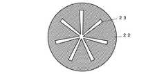
ファラデーシールドの形状は、従来知られているファラデーシールドの各種形状とすればよく、例えば誘電体が円筒形状の場合にはその誘電体の外周面に設ければよい。また、誘電体が板状の場合には図3に示すように、放射形状とすることもできる。 The shape of the Faraday shield may be various types of conventionally known Faraday shields. For example, when the dielectric is cylindrical, it may be provided on the outer peripheral surface of the dielectric. Further, when the dielectric is plate-shaped, it can be a radial shape as shown in FIG.
ファラデーシールドの素材は、アルミニウム、銀、銅といった、電気抵抗の小さい金属が望ましく、これらのうち、加工が容易という点で、特にアルミニウムが好ましい。
ファラデーシールドの厚みは、5〜200μmとすることができ、好ましくは25〜100μmの範囲とするのがよい。厚みが25μm以下になると、電気抵抗が大きくなる傾向がある。The material of the Faraday shield is desirably a metal having a low electrical resistance such as aluminum, silver, or copper, and among these, aluminum is particularly preferable in terms of easy processing.
The thickness of the Faraday shield can be 5 to 200 μm, and preferably 25 to 100 μm. When the thickness is 25 μm or less, the electric resistance tends to increase.
ファラデーシールドは接地しなくてもよく、接地してもよく、また、コンデンサを介して接地してもよい。接地の有無や方法によって、スパッタの量をコントロールすることができる。 The Faraday shield may not be grounded, may be grounded, or may be grounded via a capacitor. The amount of spatter can be controlled by the presence / absence and method of grounding.
以下、本発明に係るプラズマ反応容器の構成例について図面を参照しつつ説明する。 Hereinafter, a configuration example of a plasma reaction vessel according to the present invention will be described with reference to the drawings.
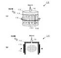
[構成例1]
図1は、本発明の一実施例に係るプラズマ反応容器10の(A)概略図、(B)概略断面図である。図1に示すプラズマ反応容器10は、誘電体12によって内部が中空である円筒形状を有しており、誘電体12の外表面にはファラデーシールド13が一体的に形成されている。ファラデーシールド13の外周には誘導コイル14が巻回(本実施例では一周回)されている。[Configuration example 1]
FIG. 1 is a (A) schematic view and (B) a schematic cross-sectional view of a
ファラデーシールド13には複数のスリット131が設けられており、このスリット131を介して誘導コイル14から発生した誘導電力が反応容器10の内部に到達し、ガス入力部16から導入される反応ガスがプラズマ化される。図1には示していないが、プラズマ反応容器10の下部には基板が配置されており、このプラズマによってスパッタリング等の各種プラズマ処理が基板に対して実行される。
なお、ファラデーシールド13には、ファラデーシールドが誘電体12の外周を一周回することがないように、切れ目132が設けられている。これによって誘導コイル14に流れる電流とは逆向きの電流がファラデーシールド13に流れることがない。The Faraday shield 13 is provided with a plurality of
The Faraday shield 13 is provided with a
プラズマ反応容器10の外部からは図示せぬ送風装置によって冷却風が導入される。冷却風は誘電体12と一体的に形成されているファラデーシールド13に向けられており、プロセス中のファラデーシールド13及び誘電体12の過熱を防止する。 Cooling air is introduced from the outside of the
[構成例2]
図2は本発明の他の実施例に係るプラズマ反応容器20の概略断面図である。
反応壁29によって形成される反応室の内部に下部電極28が設けられおり、その下部電極28上に基板27が載置されている。基板27の上部には平板状の誘電体22が基板27と平行に配置されている。そして、誘電体22の上部表面にはファラデーシールド23が一体的に形成されている。このファラデーシールド23は、平面図である図3に示すように、放射形状を有している。誘電体22及びファラデーシールド23の上部には誘導コイル24が配置されており、この誘導コイル24に高周波電力が印加されることによって反応室内にプラズマ5が形成され、基板27の処理が行われる。[Configuration example 2]
FIG. 2 is a schematic cross-sectional view of a
A
プラズマ反応容器20の外部には図示せぬ送風装置が設けられており、ファラデーシールド23及び誘電体22の表面に冷却風が導入される。これらファラデーシールド23及び誘電体22は一体的に形成されているから、この冷却風によって、誘電体22の過熱が防止される。 A blower (not shown) is provided outside the
以上、本発明に係るプラズマ反応容器について説明したが、上記説明は例に過ぎない。従って、誘電体の表面にファラデーシールドを一体的に形成するという本発明の精神内において、適宜に変形や修正を行ってももちろん構わない。 Although the plasma reaction container according to the present invention has been described above, the above description is only an example. Therefore, it is of course possible to make appropriate modifications and corrections within the spirit of the present invention that the Faraday shield is integrally formed on the surface of the dielectric.
例えば、誘電体表面がエッチングによって削られることを防止する効果をより高めることを目的として、本発明に係るプラズマ反応容器が、側壁保護膜を形成するガスおよび基板をエッチングするガスを交互に導入する保護ガス導入手段を更に備えるようにすることもできる。 For example, the plasma reaction vessel according to the present invention alternately introduces a gas for forming the sidewall protective film and a gas for etching the substrate for the purpose of further enhancing the effect of preventing the dielectric surface from being etched by etching. A protective gas introducing means may be further provided.
10、20…プラズマ反応容器
12、22…誘電体
13、23…ファラデーシールド
131…スリット
132…切れ目
14、24…誘導コイル
16…ガス入力部
27…基板
28…下部電極
29…反応壁
5…プラズマDESCRIPTION OF
Claims (3)
Translated fromJapanesePriority Applications (1)
| Application Number | Priority Date | Filing Date | Title |
|---|---|---|---|
| JP2007184418AJP2009021492A (en) | 2007-07-13 | 2007-07-13 | Plasma reaction vessel |
Applications Claiming Priority (1)
| Application Number | Priority Date | Filing Date | Title |
|---|---|---|---|
| JP2007184418AJP2009021492A (en) | 2007-07-13 | 2007-07-13 | Plasma reaction vessel |
Publications (1)
| Publication Number | Publication Date |
|---|---|
| JP2009021492Atrue JP2009021492A (en) | 2009-01-29 |
Family
ID=40360855
Family Applications (1)
| Application Number | Title | Priority Date | Filing Date |
|---|---|---|---|
| JP2007184418APendingJP2009021492A (en) | 2007-07-13 | 2007-07-13 | Plasma reaction vessel |
Country Status (1)
| Country | Link |
|---|---|
| JP (1) | JP2009021492A (en) |
Cited By (7)
| Publication number | Priority date | Publication date | Assignee | Title |
|---|---|---|---|---|
| CN103503579A (en)* | 2011-02-03 | 2014-01-08 | 泰克纳等离子系统公司 | High performance induction plasma torch |
| KR20140051250A (en)* | 2011-06-15 | 2014-04-30 | 램 리써치 코포레이션 | Power grid for plasma chamber |
| CN104302084A (en)* | 2013-07-17 | 2015-01-21 | 朗姆研究公司 | Air cooled faraday shield and methods for using the same |
| CN104576278A (en)* | 2013-10-10 | 2015-04-29 | 中微半导体设备(上海)有限公司 | Faraday shield plate and plasma treatment system using Faraday shield plate |
| JP2016081863A (en)* | 2014-10-22 | 2016-05-16 | パナソニックIpマネジメント株式会社 | Plasma processing device |
| JP2016082190A (en)* | 2014-10-22 | 2016-05-16 | パナソニックIpマネジメント株式会社 | Plasma processing equipment |
| JP2018117137A (en)* | 2013-08-07 | 2018-07-26 | 北京北方華創微電子装備有限公司Beijing Naura Microelectronics Equipment Co., Ltd. | Pre-cleaning chamber and semiconductor processing apparatus |
Citations (1)
| Publication number | Priority date | Publication date | Assignee | Title |
|---|---|---|---|---|
| JP2001085195A (en)* | 1999-09-13 | 2001-03-30 | Hitachi Ltd | High frequency discharge device and plasma processing method |
- 2007
- 2007-07-13JPJP2007184418Apatent/JP2009021492A/enactivePending
Patent Citations (1)
| Publication number | Priority date | Publication date | Assignee | Title |
|---|---|---|---|---|
| JP2001085195A (en)* | 1999-09-13 | 2001-03-30 | Hitachi Ltd | High frequency discharge device and plasma processing method |
Cited By (12)
| Publication number | Priority date | Publication date | Assignee | Title |
|---|---|---|---|---|
| CN103503579A (en)* | 2011-02-03 | 2014-01-08 | 泰克纳等离子系统公司 | High performance induction plasma torch |
| US9380693B2 (en) | 2011-02-03 | 2016-06-28 | Tekna Plasma Systems Inc. | High performance induction plasma torch |
| US10893600B2 (en) | 2011-02-03 | 2021-01-12 | Tekna Plasma Systems Inc. | High performance induction plasma torch |
| KR20140051250A (en)* | 2011-06-15 | 2014-04-30 | 램 리써치 코포레이션 | Power grid for plasma chamber |
| JP2014519717A (en)* | 2011-06-15 | 2014-08-14 | ラム リサーチ コーポレーション | Energizing grid for plasma chamber |
| US9966236B2 (en) | 2011-06-15 | 2018-05-08 | Lam Research Corporation | Powered grid for plasma chamber |
| KR101902607B1 (en)* | 2011-06-15 | 2018-09-28 | 램 리써치 코포레이션 | Power grid for plasma chamber |
| CN104302084A (en)* | 2013-07-17 | 2015-01-21 | 朗姆研究公司 | Air cooled faraday shield and methods for using the same |
| JP2018117137A (en)* | 2013-08-07 | 2018-07-26 | 北京北方華創微電子装備有限公司Beijing Naura Microelectronics Equipment Co., Ltd. | Pre-cleaning chamber and semiconductor processing apparatus |
| CN104576278A (en)* | 2013-10-10 | 2015-04-29 | 中微半导体设备(上海)有限公司 | Faraday shield plate and plasma treatment system using Faraday shield plate |
| JP2016081863A (en)* | 2014-10-22 | 2016-05-16 | パナソニックIpマネジメント株式会社 | Plasma processing device |
| JP2016082190A (en)* | 2014-10-22 | 2016-05-16 | パナソニックIpマネジメント株式会社 | Plasma processing equipment |
Similar Documents
| Publication | Publication Date | Title |
|---|---|---|
| KR102374521B1 (en) | Placing table and plasma treatment apparatus | |
| TWI778005B (en) | Plasma processing device | |
| JP2009021492A (en) | Plasma reaction vessel | |
| TWI667730B (en) | Electrostatic chuck, mounting table, plasma processing device, and manufacturing method of electrostatic chuck | |
| JP5630667B2 (en) | Substrate processing equipment | |
| KR20130077880A (en) | Plasma processing apparatus | |
| TW201448032A (en) | Plasma processing device | |
| JP7154105B2 (en) | Cleaning method and plasma processing apparatus | |
| JP2014195047A (en) | Mounting table and plasma processing device | |
| TW201436034A (en) | Substrate support for plasma etch operations | |
| KR20160065382A (en) | Support unit and apparatus for treating substrate with the support unit | |
| TWM459518U (en) | Faraday shielding apparatus and plasma processing equipment with temperature reduction function | |
| WO2013172456A1 (en) | Plasma processing apparatus and plasma processing method | |
| US20180019099A1 (en) | Plasma processing apparatus | |
| JP2020043328A (en) | Plasma processing equipment | |
| KR102015381B1 (en) | Plasma generating device and apparatus for treating substrate comprising the same | |
| KR102799000B1 (en) | Plasma processing apparatus | |
| KR101569886B1 (en) | Substrate supporting unit and substrate treating apparatus including the same | |
| US6864640B2 (en) | Plasma processing method and apparatus thereof | |
| KR20210027648A (en) | Apparatus for treating substrate and method for cleaning chamber | |
| KR101909473B1 (en) | Apparatus for treating substrate | |
| JP2011129515A (en) | Electrode for discharge lamp | |
| JP6304550B2 (en) | Plasma processing equipment | |
| KR101375539B1 (en) | Plasma ignition | |
| KR101408790B1 (en) | Apparatus for treating substrate |
Legal Events
| Date | Code | Title | Description |
|---|---|---|---|
| A621 | Written request for application examination | Free format text:JAPANESE INTERMEDIATE CODE: A621 Effective date:20100331 | |
| RD02 | Notification of acceptance of power of attorney | Effective date:20100331 Free format text:JAPANESE INTERMEDIATE CODE: A7422 | |
| A131 | Notification of reasons for refusal | Free format text:JAPANESE INTERMEDIATE CODE: A131 Effective date:20110920 | |
| A977 | Report on retrieval | Free format text:JAPANESE INTERMEDIATE CODE: A971007 Effective date:20110922 | |
| A02 | Decision of refusal | Free format text:JAPANESE INTERMEDIATE CODE: A02 Effective date:20120403 |