JP2009016863A - Non-volatile reprogrammable interconnect cell with FN tunnel and sensing device - Google Patents
Non-volatile reprogrammable interconnect cell with FN tunnel and sensing deviceDownload PDFInfo
- Publication number
- JP2009016863A JP2009016863AJP2008226043AJP2008226043AJP2009016863AJP 2009016863 AJP2009016863 AJP 2009016863AJP 2008226043 AJP2008226043 AJP 2008226043AJP 2008226043 AJP2008226043 AJP 2008226043AJP 2009016863 AJP2009016863 AJP 2009016863A
- Authority
- JP
- Japan
- Prior art keywords
- column
- voltage
- row
- cell
- floating gate
- Prior art date
- Legal status (The legal status is an assumption and is not a legal conclusion. Google has not performed a legal analysis and makes no representation as to the accuracy of the status listed.)
- Pending
Links
Images


Classifications
- G—PHYSICS
- G11—INFORMATION STORAGE
- G11C—STATIC STORES
- G11C16/00—Erasable programmable read-only memories
- G11C16/02—Erasable programmable read-only memories electrically programmable
- G11C16/04—Erasable programmable read-only memories electrically programmable using variable threshold transistors, e.g. FAMOS
- G11C16/0408—Erasable programmable read-only memories electrically programmable using variable threshold transistors, e.g. FAMOS comprising cells containing floating gate transistors
- G11C16/0441—Erasable programmable read-only memories electrically programmable using variable threshold transistors, e.g. FAMOS comprising cells containing floating gate transistors comprising cells containing multiple floating gate devices, e.g. separate read-and-write FAMOS transistors with connected floating gates
- H—ELECTRICITY
- H10—SEMICONDUCTOR DEVICES; ELECTRIC SOLID-STATE DEVICES NOT OTHERWISE PROVIDED FOR
- H10B—ELECTRONIC MEMORY DEVICES
- H10B69/00—Erasable-and-programmable ROM [EPROM] devices not provided for in groups H10B41/00 - H10B63/00, e.g. ultraviolet erasable-and-programmable ROM [UVEPROM] devices
Landscapes
- Engineering & Computer Science (AREA)
- Microelectronics & Electronic Packaging (AREA)
- Design And Manufacture Of Integrated Circuits (AREA)
- Non-Volatile Memory (AREA)
- Logic Circuits (AREA)
- Semiconductor Memories (AREA)
- Read Only Memory (AREA)
Abstract
Translated fromJapaneseDescription
Translated fromJapanese本発明は、現場でプログラムできる集積回路、特に現場でプログラムできるゲートアレー(FPGA)に係り、より詳細には、FPGAのスイッチング素子として使用されるフローティングゲートMOSトランジスタに係る。 The present invention relates to on-site programmable integrated circuits, and more particularly to on-site programmable gate arrays (FPGAs), and more particularly to floating gate MOS transistors used as switching elements in FPGAs.
一般に、FPGAは、論理素子と、数千又は数万のプログラム可能な相互接続部を伴う配線相互接続部とのアレーを有し、ユーザはFPGAを定められた機能をもつ集積回路へと構成することができる。各々のプログラム可能な相互接続部即ちスイッチは、集積回路の2つの回路ノードを接続して、配線相互接続をメーク(又はブレーク)したり、或いは論理素子の機能(1つ又は複数)をセットしたりすることができる。 In general, an FPGA has an array of logic elements and wiring interconnects with thousands or tens of thousands of programmable interconnects, and the user configures the FPGA into an integrated circuit with a defined function. be able to. Each programmable interconnect or switch connects two circuit nodes of an integrated circuit to make (or break) a wiring interconnect, or to set the function (s) of a logic element Can be.
FPGAは、プログラム可能な相互接続部としてメモリセル又はアンチフューズのいずれかを使用する。メモリセルは再プログラム可能であり、そしてアンチフューズは1回しかプログラムできない。新規な不揮発性メモリ型のプログラム可能な相互接続部が、本発明の譲受人に譲渡されたロバートJ.リップ、リチャードD.フリーマン、ロバートU.ブローズ、ジョンM.ケイウッド及びジョセフG.ノーラン三世の1996年11月21日出願の「汎用の不揮発性の再プログラム可能なスイッチ(A GENERAL PURPOSE, NON-VOLATILE REPROGRAMMABLE SWITCH) 」と題する米国特許出願第08/754,116号に開示されている。この特許出願に開示されたFPGAでは、不揮発性の再プログラム可能なトランジスタメモリ(NVM)セルを使用し、FPGAの配線及び回路素子をランダムに相互接続するための汎用のスイッチング素子が形成される。基本的に、NVMセルは、充電及び/又は放電できるフローティングゲートをもつMOSトランジスタを有している。フローティングゲートの充電及び/又は放電は、NVM技術の不揮発性プログラミング特徴を与える。 FPGAs use either memory cells or antifuses as programmable interconnects. The memory cell can be reprogrammed and the antifuse can be programmed only once. A novel non-volatile memory type programmable interconnect is described in Robert J., assigned to the assignee of the present invention. Lip, Richard D. Freeman, Robert U. Blows, John M. Kaywood and Joseph G. Nolan III disclosed in US patent application Ser. No. 08 / 754,116 entitled “A GENERAL PURPOSE, NON-VOLATILE REPROGRAMMABLE SWITCH” filed on Nov. 21, 1996. Yes. In the FPGA disclosed in this patent application, a non-volatile reprogrammable transistor memory (NVM) cell is used to form a general-purpose switching element for randomly interconnecting the wiring and circuit elements of the FPGA. Basically, an NVM cell has a MOS transistor with a floating gate that can be charged and / or discharged. Floating gate charging and / or discharging provides the non-volatile programming feature of NVM technology.
FPGA、実際には、いかなる集積回路においても、FPGAの素子は、回路を効率的にレイアウトするためにできるだけコンパクトであると共に、できるだけ容易に製造できることが重要である。本発明の譲受人に譲渡されたロバートU.ブローズ氏の「FNトンネリング及びプログラミング式の不揮発性の再プログラム可能な相互接続セル(Non-Volatile Reprogrammable Interconnect Cell With FN Tunneling and Programming) 」と題する1995年7月28日出願の米国特許出願第08/508,914号は、上記米国特許出願第08/754,116号に開示されたプログラム可能な相互接続部の1つの非常にコンパクトなセルに向けられる。各々選択的にプログラムできるこのような相互接続部の効率的なアレーが達成される。各プログラム可能な相互接続セルは、第1のMOSトランジスタを有し、このMOSトランジスタは、第1及び第2の回路ノードに各々接続された第1及び第2のソース/ドレインと、第1のMOSトランジスタをゲートの電荷量に応じてオフ及びオンに切り換えるためのフローティングゲートとを有する。又、セルは、第1のMOSトランジスタのフローティングゲートに接続されると共に、トンネル酸化物層を経てプログラミング/消去ラインに接続されたトンネルデバイスと、上記フローティングゲートに容量性結合された制御ゲートと、上記酸化物層のトンネル作用を制御可能に禁止するための少なくとも1つのトンネル制御ラインとを有する。このトンネル制御ライン及びプログラミング/消去ラインは、トンネル酸化物層の下の領域に接近しているがそこから横方向に変位されたPN接合を形成する。逆バイアスのもとでは、接合の電荷空乏領域がトンネル酸化物の下の領域を経て延び、トンネル作用を阻止する。これは、各プログラム可能な相互接続部を選択的にプログラムできるようにする。 In an FPGA, in fact, in any integrated circuit, it is important that the elements of the FPGA are as compact as possible and can be manufactured as easily as possible to efficiently lay out the circuit. Robert U.S. assigned to the assignee of the present invention. US patent application Ser. No. 08/08, filed Jul. 28, 1995, entitled “FN Tunneling and Programming Non-Volatile Reprogrammable Interconnect Cell With FN Tunneling and Programming” 508,914 is directed to one very compact cell of the programmable interconnect disclosed in the above-mentioned US patent application Ser. No. 08 / 754,116. An efficient array of such interconnects, each of which can be selectively programmed, is achieved. Each programmable interconnect cell has a first MOS transistor, the MOS transistor having first and second source / drains connected to the first and second circuit nodes, respectively, and a first And a floating gate for switching the MOS transistor off and on in accordance with the amount of charge of the gate. The cell is also connected to the floating gate of the first MOS transistor and connected to the programming / erasing line through the tunnel oxide layer; a control gate capacitively coupled to the floating gate; And at least one tunnel control line for controllably inhibiting the tunneling of the oxide layer. The tunnel control line and programming / erase line form a PN junction that is close to, but laterally displaced from, the region below the tunnel oxide layer. Under reverse bias, the charge depletion region of the junction extends through the region below the tunnel oxide, preventing tunneling. This allows each programmable interconnect to be selectively programmed.
本発明は、製造収率、信頼性、プログラミング速度、スレッシュホールド限界及びコストを改善したFPGAセル及びアレー構造体の改良に向けられる。セルは、共通のフローティングゲートを有するゲートスイッチトランジスタ及びゲート感知トランジスタを備え、感知トランジスタは、トランジスタのドレイン及びフローティングゲートへの及びそこからのファウラー・ノルトハイム電子トンネル作用によりスイッチトランジスタのプログラミング及び消去も与える。セル又はFPGAタイルのアレーにおいては、2本の列ラインが各列における感知トランジスタのソース及びドレイン領域に各々接続され、これは、感知トランジスタ及びスイッチトランジスタのスレッシュホールド電圧を感知し、ひいては、スイッチトランジスタのプログラム状態又は消去状態を測定するのに使用される。 The present invention is directed to improvements in FPGA cells and array structures with improved manufacturing yield, reliability, programming speed, threshold limits and cost. The cell comprises a gate switch transistor and a gate sense transistor having a common floating gate, which also provides programming and erasure of the switch transistor by Fowler-Nordheim electron tunneling to and from the transistor drain and floating gate. . In an array of cells or FPGA tiles, two column lines are connected to the source and drain regions of the sense transistors in each column, respectively, which sense the threshold voltages of the sense transistors and switch transistors, and thus switch transistors. It is used to measure the program state or erase state.
本発明の特徴によれば、セルのプログラム障害は、行選択/非選択電圧ウインドウを列選択/非選択電圧ウインドウと電圧VUUD だけ重畳することにより減少される。この電圧は、行及び列が両方とも非選択であるプログラムビットのストレスを増加するが、行又は列のみ(両方ではない)が非選択である消去ビットのストレスを減少する。ここで使用する「ストレス」とは、時間と共に障害を生じる可能性を有する電界を意味する。又、ここで使用する「障害」とは、特定の時間中に外部から付与される1組のバイアス状態によりフローティングゲートから電荷が除去(又は追加)されるために生じるFPGAセルのスレッシュホールド電圧の不所望な変化を意味する。According to a feature of the present invention, cell programming failure is reduced by superimposing the row selection / non-selection voltage window by the column V /UD voltage window and the voltage VUUD . This voltage increases the stress of program bits where both rows and columns are unselected, but reduces the stress of erase bits where only rows or columns (but not both) are unselected. As used herein, “stress” means an electric field that has the potential to cause failure over time. As used herein, “failure” refers to the threshold voltage of an FPGA cell that is generated when a charge is removed (or added) from a floating gate by a set of externally applied bias states during a specific time. It means an undesired change.
本発明並びにその目的及び特徴は、添付図面を参照した以下の詳細な説明及び特許請求の範囲から容易に明らかとなろう。
図1は、スイッチトランジスタ10と、ファウラー・ノルトハイムトンネルデバイス及び感知トランジスタ12とを含む本発明によるFPGAセルを示す回路図である。スイッチトランジスタは、そのトランジスタのドレイン及びソース領域に各々接続された接点14及び16を有し、そして感知トランジスタ12は、そのトランジスタのドレイン及びソース領域に各々接続された接点18及び20を有する。感知トランジスタのドレインは、ドレインの列(メタル)ライン22にも接続され、そしてそのソースは、ソースの列(メタル)ライン24にも接続される。これら列ライン22、24は、1つの列における感知トランジスタの全てのソース及びドレイン領域に接続される。スイッチトランジスタ10及び感知増幅器12は、共通のフローティングゲート26を共用し、このフローティングゲートは、スイッチトランジスタ10の制御ゲート28と、感知トランジスタ12の制御ゲート30との間に配置される。これら制御ゲートは、行(ポリ2)ライン32に接続される。The invention and its objects and features will become more readily apparent from the following detailed description and appended claims when taken with the accompanying drawings.
FIG. 1 is a circuit diagram illustrating an FPGA cell according to the present invention including a
図2の感知トランジスタの断面図に明確に示されたように、感知トランジスタのフローティングゲート26は、感知トランジスタのN+ドープされたドレイン34及び/又はソース35に密接当接又は重畳して配置され、厚みが80Åないし120Å程度の特殊なトンネル酸化物36がフローティングゲート26とN+ドレイン34とを分離し、矢印38で示すように、フローティングゲートとドレイン領域との間に電子のトンネル作用が容易に生じるようにしている。従って、FPGAセルの消去は、ドレインソース及びチャンネル領域からフローティングゲートへの電子のトンネル作用によって生じる。FPGAセルのプログラミングは、フローティングゲートからドレイン及び/又はソースへの電子のトンネル作用によって生じる。 As clearly shown in the cross-sectional view of the sensing transistor of FIG. 2, the
図3は、図1のFPGAセルのレイアウトの平面図である。スイッチトランジスタ10及び感知トランジスタ12は、半導体ウェハにおいて離間水平整列状態にあり、フローティングゲート26は、トランジスタ10のソース及びドレインと感知トランジスタ12のソース及びドレインとの間のチャンネル領域に重畳する第1のポリシリコンライン(ポリ1)を含む。ポリ1ラインは、セルの各側で終り、隣接セルへ続かない。2つのトランジスタの制御ゲート28、30は、第2のポリシリコンライン(ポリ2)32によって形成され、これは、ポリ1ラインの上に延び、そしてそれと自己整列される。ポリ2ラインは、その行に配列されたセルの全てのトランジスタへと続く。ドレイン列ライン22は、ドレインへの接点18に接続され、そしてその列の全ての感知トランジスタのドレイン端子に接触するように垂直方向に続く。同様に、ソース列メタルライン24は、ソース接点20に係合し、そしてその列の感知トランジスタの全てのソース領域に接触するように垂直方向に延びる。従って、FPGAセルのある列において、全ての感知トランジスタのソースは、ソース列と称する1つの列ラインに接続され、そして全てのドレインは、ドレイン列と称する第2の列ラインに接続される。図3に示すセルは、これも又プログラム及び消去機能を遂行する隣接感知デバイスに対し共用ソース接点の半分と共用ドレイン接点の半分とを含む。上記したように、感知デバイスは、スイッチトランジスタがFPGAアレーに配線されアクセスできないので、各FPGAセルのプログラムされた状態又は消去された状態をテストするために必要とされる。 FIG. 3 is a plan view of the layout of the FPGA cell of FIG. The
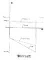
FPGAタイルは、例えば、コアタイルの場合に32行x5列のFPGAセルのアレーより成る。図4及び5は、各々、このようなアレーにおける2列及び4行の回路図及び平面図である。図1ないし3の参照番号が、図4及び5において全てのポリ1フローティングゲート26、ポリ2行ライン32、ドレイン列ライン22及びソースメタル列ライン24と共に使用される。4つの行は、Rowi ないしRowi+3 で示され、ドレイン列は、DCOLj 及びDCOLj+1 で示され、そしてソース列は、SCOLj 及びSCOLj+1 で指示されている。感知トランジスタのアレーにおいて各ビットのプログラム及び消去された感知トランジスタのスレッシュホールドの測定は、列の各非選択ビットの感知トランジスタを「オフ」にバイアスしそして選択ビットを限界処理(margining) することによりNOR ROMがアクセスされるのと同様に実行される。この測定「限界処理」は、選択されたセルの制御ゲート(行)電圧を変えながら、ドレイン電流がある基準レベルの上となるか下となるかを検出することにより行われる。行バイアスは、多数の動作モードをもつ列ドライバにより駆動される。それらは、「消去」中にはアレーに対して高い正の電圧を供給しなければならず、「プログラム」及び「読み取り」中には正及び負の電圧を行に供給しなければならず、そして「動作」モード中には一定の正のバイアスを供給しなければならない。列バイアスは列ドライバにより付与される。プログラムするためには、列が正の電圧に対して対として駆動されねばならない。対の一方は、その他方が接地レベルに保持される間に「読み取り」中の電流を感知しながら低い正の電圧レベルに強制される。他の全ての時間には、それらが両方とも接地又は開路される。For example, in the case of a core tile, the FPGA tile includes an array of FPGA cells of 32 rows × 5 columns. 4 and 5 are a circuit diagram and a plan view of two columns and four rows, respectively, in such an array. 1 through 3 are used with all
テーブル1は、全ての動作モードに対しおおよその行及び列並びにピーク電圧レベルを示す。プログラムの障害は、行選択/非選択ウインドウ電圧を列選択/非選択ウインドウ電圧とVUUD だけ重畳することによって許容レベルに減少される。この電圧は、行及び列の両方が非選択であるプログラムビットにはストレスを及ぼすが、行又は列のみ(両方ではない)が非選択である消去ビットのプログラミングストレスを減少する。これらの方式は、理想的な例であり、周辺回路のブレークダウン電圧や、行対列のプログラミング時間要素を考慮して、電圧レベルを調整することができる。
テーブル1
消去 プログラム 読み取り/限界 動作
選択行 VERASE -VP /(2*RR ) -VR から+VR 0VからVCC
へ傾斜 へ傾斜
選択列対 両方=0V +VP /(2*(1-Rc )) ドレイン列≒1V 両方=0V
へ両方傾斜 ソース列=0V
非選択行 - VUUP -(VR +Δ) -
非選択列 - 0V 0V -Table 1 shows the approximate row and column and peak voltage levels for all operating modes. Program failures are reduced to an acceptable level by superimposing the row selection / non-selection window voltage by the column selection / non-selection window voltage by VUUD . This voltage stresses program bits where both rows and columns are unselected, but reduces the programming stress of erase bits where only rows or columns (but not both) are unselected. These methods are ideal examples, and the voltage level can be adjusted in consideration of the breakdown voltage of the peripheral circuit and the row-to-column programming time factor.
Table 1
Erase Program Read / Limit Operation
Selected row VERASE -VP / (2 * RR ) -VR to + VR 0V to VCC
Tilt to tilt to tilt
Selected column pair Both = 0V + VP / (2 * (1-Rc )) Drain column ≒ 1V Both = 0V
Both slopes Source row = 0V
Unselectedrow-VUUP-(VR+ Δ)-
Non-selected column-0V 0V-
図6は、「消去」中に行に印加される電圧の波形を示す。これはバルク動作であるから、障害は生じない。消去中に、感知トランジスタのドレイン/ソース、及び表面を逆に有するチャンネルから、フローティングポリシリコンゲートへと電子のトンネル作用が生じる。これは、スイッチ及び感知トランジスタのフローティングゲートに負の電荷を残し、行(制御ゲート)からフローティングゲートに相補的な電圧が接続されない限りそれらを「オフ」にする。 FIG. 6 shows the waveform of the voltage applied to the row during “erase”. Since this is a bulk operation, no failure occurs. During erasure, electron tunneling occurs from the drain / source of the sense transistor and the channel having the opposite surface to the floating polysilicon gate. This leaves negative charges on the floating gates of the switch and sense transistor, turning them off unless a complementary voltage is connected from the row (control gate) to the floating gate.
書き込み又は「プログラミング」動作は、選択、消去されたスイッチ及び感知トランジスタを「オン」状態に戻すのに使用される。これは、行に負の電圧をそして列対に正の電圧を強制することにより行われる。フローティングゲートは、感知トランジスタのドレイン及びソースに対して負に駆動され、そしてフローティングゲートからドレイン接合へ電子のトンネル作用が生じ、ドレイン接合は、図2に示すように、片側又は両側においてフローティングゲート及びポリシリコンゲート積層体の下に述べるように処理される。この動作は、フローティングゲートに正の正味電荷を残し、これは、スイッチ及び感知トランジスタを「オン」状態にする。 A write or “programming” operation is used to return the selected, erased switch and sense transistor to the “on” state. This is done by forcing a negative voltage on the row and a positive voltage on the column pair. The floating gate is driven negatively with respect to the drain and source of the sensing transistor and electron tunneling occurs from the floating gate to the drain junction, the drain junction being connected to the floating gate on one or both sides as shown in FIG. Processed as described below the polysilicon gate stack. This action leaves a net positive charge on the floating gate, which turns the switch and sense transistor “on”.
図7は、「プログラム」動作中の選択された行及び列に対する波形を示す。行(制御ゲート)は、負に傾斜され、一方、列ラインは、正に傾斜されて、フローティングゲートから電子を除去し、これは、プログラミング後にフローティングゲートに正の正味電荷を残す。 FIG. 7 shows waveforms for selected rows and columns during a “program” operation. The row (control gate) is tilted negative, while the column line is tilted positive to remove electrons from the floating gate, which leaves a positive net charge on the floating gate after programming.
図8は、「プログラム」動作中に選択された行及び非選択の列に適用される波形を示す。
図9は、「プログラム」動作中に非選択の行及び選択された列に対する電圧波形を示す。
図10は、「プログラム」動作中に行及び列の両方が非選択の場合の電圧波形を示す。FIG. 8 shows waveforms applied to selected rows and unselected columns during a “program” operation.
FIG. 9 shows voltage waveforms for unselected rows and selected columns during a “program” operation.
FIG. 10 shows the voltage waveform when both row and column are unselected during a “program” operation.
読み取り限界処理動作中に、選択されたタイル(図4)の感知トランジスタは「オン」にされ、そしてアレーの残り部分における全ての非選択の行は負の電圧にされて、それらを「オフ」にする。選択された行の電圧は、「消去」ビットに対して高い傾斜にされる。バイアスが低い電圧にセットされた状態で列がスレッシュホールド電流に達すると、行電圧がそのビットの「消去限界」として記録される。同様に、行電圧は、プログラムされたビットに対して負に傾斜され、そしてスレッシュホールド電流の電圧が「プログラム限界」となる。 During the read limit processing operation, the sense transistors of the selected tile (FIG. 4) are turned “on” and all unselected rows in the rest of the array are brought to a negative voltage to “off” them. To. The voltage of the selected row is ramped high with respect to the “erase” bit. When the column reaches the threshold current with the bias set to a low voltage, the row voltage is recorded as the “erase limit” for that bit. Similarly, the row voltage is negatively ramped with respect to the programmed bit, and the threshold current voltage becomes the “program limit”.
FPGAの動作モードでは、全ての行に正のDCバイアスが印加される。これは、スイッチの動作の電圧ウインドウを、消去されたセルに対する弱い「オフ」から、プログラムされたセルに対する強い「オン」へシフトし、そして「オフ」のスイッチの電流を妨げずに全振幅信号を「オン」のスイッチに通過できるようにする。
プログラミング中に行及び列に印加される電圧の選択/非選択ウインドウを重畳することにより書き込み障害が最小にされる。これは、行又は列のいずれかが選択された非選択のセルにおける障害領域を減少するが、行も列も選択されないセルの障害バイアスを増加させる。行及び列の電圧ウインドウは、全ての場合のプログラミング障害を最小にするように重畳される。In the FPGA operation mode, a positive DC bias is applied to all rows. This shifts the voltage window of the switch operation from a weak “off” for the erased cell to a strong “on” for the programmed cell, and the full amplitude signal without disturbing the “off” switch current. Can be passed through the “on” switch.
Write failures are minimized by superimposing selected / unselected windows of voltages applied to rows and columns during programming. This reduces the failure area in unselected cells where either row or column is selected, but increases the failure bias of cells where no row or column is selected. The row and column voltage windows are superimposed to minimize programming disturbances in all cases.
逆極性の時間的にリニアな電圧傾斜を選択された行及び列に印加することにより、他の波形の作用に対しその選択された行又は列における非選択のセルからの電荷除去が最小にされる。
従来の行プログラミングに代わって列プログラミングを使用して全体的な障害を減少することができる。この解決策の効果は、行及び列の結合比の相違により非選択の行の障害が非選択の列よりも大きくなることである。しかしながら、この解決策の欠点は、回路の面積、テストの複雑さ及びテスト時間に関して、列のプログラミングの実施にコストがかかることである。By applying a time-linear voltage ramp of opposite polarity to the selected row and column, charge removal from unselected cells in that selected row or column is minimized relative to the effects of other waveforms. The
Column programming can be used in place of traditional row programming to reduce overall failure. The effect of this solution is that non-selected row faults are larger than non-selected columns due to differences in row and column coupling ratios. However, the disadvantage of this solution is that the implementation of the column programming is expensive with respect to circuit area, test complexity and test time.
上記したFPGAセル及びアレーは、若干のマスクと共に従来のEEPROM−CMOS処理を用いて容易に製造される。プログラミング及び消去にトンネル酸化物を使用することにより、非自己整列のEPROMセル構造体及びそれに関連したマスキング処理段階の使用が回避される。2デバイスのセル構造は、面積が小さく、消去及びプログラミングの両方の状態に対して各ビットの完全な限界処理が達成される。 The above-described FPGA cells and arrays are easily manufactured using conventional EEPROM-CMOS processing with some masks. By using tunnel oxide for programming and erasing, the use of non-self-aligned EPROM cell structures and associated masking steps are avoided. The two-device cell structure is small in area and complete limit processing of each bit is achieved for both erase and programming states.
特定の実施形態を参照して本発明を説明したが、これは、単に本発明を例示するものに過ぎず、本発明をこれに限定するものではない。請求の範囲に規定された本発明の真の精神及び範囲から逸脱せずに種々の変更や応用がなされることが当業者に明らかであろう。 Although the present invention has been described with reference to particular embodiments, this is merely illustrative of the invention and is not intended to limit the invention thereto. It will be apparent to those skilled in the art that various modifications and variations can be made without departing from the true spirit and scope of the invention as defined in the claims.
10 スイッチトランジスタ
12 感知トランジスタ
14、16、18、20 接点
26 共通のフローティングゲート
28、30 制御ゲート
34 ドレイン
35 ソース
36 トンネル酸化物10
Claims (2)
Translated fromJapaneseそれぞれのセルが同じ行にあるセルの第1の電界効果トランジスタと整列した第1のフローティングゲート電界効果トランジスタ、及び同じ行にあるセルの第2の電界効果トランジスタと整列した第2のフローティングゲート電界効果トランジスタを有しており、セルの前記第1及び第2の電界効果トランジスタが同じ列にあるセルの第1及び第2のフローティングゲート電界効果トランジスタと整列しているものにおいて、
非選択の相互接続部について少ない障害で相互接続部を選択的にプログラムする方法であって、
a)第1の2つの電圧レベルの間の電圧を列選択ラインに印加し、これによって1つの列を選択する段階と、
b)第2の2つの電圧レベルの間の電圧を行選択ラインを印加し、これによって1つの行を選択する段階とを備え、
前記第1の2つの電界レベルと前記第2の2つの電圧レベルとを電圧のオフセットを有するように重畳させ、これによって、ただ1つの列と行が選択された場合の列と行にあるセルが減少したプログラム電圧ストレスを有するようにする方法。An array of programmable interconnects for selectively connecting circuit nodes of an integrated circuit and arranged in rows and columns, each programmable to connect and disconnect circuit nodes In an array containing a number of interconnected cells,
A first floating gate field effect transistor aligned with a first field effect transistor of each cell in the same row and a second floating gate field aligned with a second field effect transistor of the cell in the same row Comprising an effect transistor, wherein the first and second field effect transistors of the cell are aligned with the first and second floating gate field effect transistors of the cells in the same column;
A method of selectively programming an interconnect with few failures for an unselected interconnect,
a) applying a voltage between the first two voltage levels to the column select line, thereby selecting a column;
b) applying a row selection line to a voltage between the second two voltage levels, thereby selecting a row;
The first two electric field levels and the second two voltage levels are superimposed with a voltage offset so that cells in columns and rows when only one column and row are selected To have reduced program voltage stress.
Applications Claiming Priority (1)
| Application Number | Priority Date | Filing Date | Title |
|---|---|---|---|
| US08/829,374US5838040A (en) | 1997-03-31 | 1997-03-31 | Nonvolatile reprogrammable interconnect cell with FN tunneling in sense |
Related Parent Applications (1)
| Application Number | Title | Priority Date | Filing Date |
|---|---|---|---|
| JP08132798ADivisionJP4347922B2 (en) | 1997-03-31 | 1998-03-27 | Nonvolatile reprogrammable interconnect cell with FN tunnel and sensing device |
Publications (1)
| Publication Number | Publication Date |
|---|---|
| JP2009016863Atrue JP2009016863A (en) | 2009-01-22 |
Family
ID=25254365
Family Applications (2)
| Application Number | Title | Priority Date | Filing Date |
|---|---|---|---|
| JP08132798AExpired - LifetimeJP4347922B2 (en) | 1997-03-31 | 1998-03-27 | Nonvolatile reprogrammable interconnect cell with FN tunnel and sensing device |
| JP2008226043APendingJP2009016863A (en) | 1997-03-31 | 2008-09-03 | Non-volatile reprogrammable interconnect cell with FN tunnel and sensing device |
Family Applications Before (1)
| Application Number | Title | Priority Date | Filing Date |
|---|---|---|---|
| JP08132798AExpired - LifetimeJP4347922B2 (en) | 1997-03-31 | 1998-03-27 | Nonvolatile reprogrammable interconnect cell with FN tunnel and sensing device |
Country Status (3)
| Country | Link |
|---|---|
| US (1) | US5838040A (en) |
| JP (2) | JP4347922B2 (en) |
| DE (1) | DE19813653B4 (en) |
Families Citing this family (23)
| Publication number | Priority date | Publication date | Assignee | Title |
|---|---|---|---|---|
| JPH11121722A (en)* | 1997-10-17 | 1999-04-30 | Mitsubishi Electric Corp | Gate array and method of manufacturing semiconductor integrated circuit using gate array |
| US6137728A (en)* | 1998-12-04 | 2000-10-24 | Gatefield Corporation | Nonvolatile reprogrammable interconnect cell with programmable buried source/drain in sense transistor |
| US6072720A (en)* | 1998-12-04 | 2000-06-06 | Gatefield Corporation | Nonvolatile reprogrammable interconnect cell with programmable buried bitline |
| US6125059A (en)* | 1999-05-14 | 2000-09-26 | Gatefield Corporation | Method for erasing nonvolatile memory cells in a field programmable gate array |
| DE59914039D1 (en)* | 1999-10-20 | 2007-01-18 | Infineon Technologies Ag | Programmable FPGA cell |
| US6515912B1 (en)* | 2000-04-14 | 2003-02-04 | Koninklijke Philips Electronics N.V. | Semiconductor device |
| US6327178B1 (en) | 2000-07-18 | 2001-12-04 | Micron Technology, Inc. | Programmable circuit and its method of operation |
| US6597609B2 (en) | 2001-08-30 | 2003-07-22 | Micron Technology, Inc. | Non-volatile memory with test rows for disturb detection |
| DE10146216A1 (en)* | 2001-09-19 | 2003-04-10 | Infineon Technologies Ag | Semiconductor structure, memory arrangement and method for producing a semiconductor structure |
| DE60315985T2 (en)* | 2002-07-08 | 2008-05-21 | Nxp B.V. | CLEARABLE AND PROGRAMMABLE NON VOLATILE CELL |
| US6970383B1 (en) | 2003-06-10 | 2005-11-29 | Actel Corporation | Methods of redundancy in a floating trap memory element based field programmable gate array |
| US7430137B2 (en)* | 2004-09-09 | 2008-09-30 | Actel Corporation | Non-volatile memory cells in a field programmable gate array |
| US7161841B1 (en)* | 2005-06-29 | 2007-01-09 | Actel Corporation | Method for erasing programmable interconnect cells for field programmable gate arrays using reverse bias voltage |
| US7245535B2 (en)* | 2005-09-21 | 2007-07-17 | Actel Corporation | Non-volatile programmable memory cell for programmable logic array |
| EP2047476B1 (en)* | 2006-07-27 | 2010-12-22 | STMicroelectronics SA | Charge retention circuit for time measurement |
| FR2904464A1 (en)* | 2006-07-27 | 2008-02-01 | St Microelectronics Sa | EEPROM LOAD RETENTION CIRCUIT FOR TIME MEASUREMENT |
| FR2904463A1 (en)* | 2006-07-27 | 2008-02-01 | St Microelectronics Sa | PROGRAMMING A LOAD RETENTION CIRCUIT FOR TIME MEASUREMENT |
| JP4512752B2 (en) | 2008-10-30 | 2010-07-28 | 独立行政法人産業技術総合研究所 | Reconfigurable integrated circuit |
| US8410815B2 (en) | 2010-12-02 | 2013-04-02 | Infineon Technologies Ag | Transistor arrangement and integrated circuit |
| EP3070846B1 (en) | 2013-11-15 | 2020-04-01 | Asahi Kasei Microdevices Corporation | Voltage detector and method for setting baseline voltage |
| CN107302003A (en)* | 2017-06-22 | 2017-10-27 | 中国电子科技集团公司第五十八研究所 | Radioresistance Sence Switch type nFLASH switch element structures and preparation method thereof |
| CN107180833B (en)* | 2017-06-22 | 2021-05-25 | 中国电子科技集团公司第五十八研究所 | A kind of radiation-resistant Sense-Switch type pFLASH switch unit structure and preparation method thereof |
| CN111668223A (en)* | 2020-06-16 | 2020-09-15 | 中国电子科技集团公司第五十八研究所 | A high-power, low-leakage Sense-Switch pFLASH cell structure |
Citations (2)
| Publication number | Priority date | Publication date | Assignee | Title |
|---|---|---|---|---|
| JPS6432494A (en)* | 1987-07-27 | 1989-02-02 | Mitsubishi Electric Corp | Non-volatile semiconductor storage device |
| WO1997005662A1 (en)* | 1995-07-28 | 1997-02-13 | Zycad Corporation | Nonvolatile reprogrammable interconnect cell with fn tunneling and programming method thereof |
Family Cites Families (12)
| Publication number | Priority date | Publication date | Assignee | Title |
|---|---|---|---|---|
| DE3136517C2 (en)* | 1980-09-26 | 1985-02-07 | Tokyo Shibaura Denki K.K., Kawasaki, Kanagawa | Non-volatile semiconductor memory device |
| US4695979A (en)* | 1985-09-09 | 1987-09-22 | Texas Instruments Incorporated | Modified four transistor EEPROM cell |
| US5016217A (en)* | 1988-05-17 | 1991-05-14 | Ict International Cmos Technology, Inc. | Logic cell array using CMOS EPROM cells having reduced chip surface area |
| US5101378A (en)* | 1988-06-15 | 1992-03-31 | Advanced Micro Devices, Inc. | Optimized electrically erasable cell for minimum read disturb and associated method of sensing |
| JPH02199698A (en)* | 1989-01-30 | 1990-08-08 | Kawasaki Steel Corp | Semiconductor memory device |
| JP2829156B2 (en)* | 1991-07-25 | 1998-11-25 | 株式会社東芝 | Redundancy circuit for nonvolatile semiconductor memory device |
| US5247478A (en)* | 1992-03-06 | 1993-09-21 | Altera Corporation | Programmable transfer-devices |
| US5329487A (en)* | 1993-03-08 | 1994-07-12 | Altera Corporation | Two transistor flash EPROM cell |
| WO1996001499A1 (en)* | 1994-07-05 | 1996-01-18 | Zycad Corporation | A general purpose, non-volatile reprogrammable switch |
| US5488586A (en)* | 1994-10-24 | 1996-01-30 | Altera Corporation | Method and apparatus for erasing an array of electrically erasable programmable read only memory cells |
| US5594363A (en)* | 1995-04-07 | 1997-01-14 | Zycad Corporation | Logic cell and routing architecture in a field programmable gate array |
| US5640344A (en)* | 1995-07-25 | 1997-06-17 | Btr, Inc. | Programmable non-volatile bidirectional switch for programmable logic |
- 1997
- 1997-03-31USUS08/829,374patent/US5838040A/ennot_activeExpired - Lifetime
- 1998
- 1998-03-27JPJP08132798Apatent/JP4347922B2/ennot_activeExpired - Lifetime
- 1998-03-27DEDE19813653Apatent/DE19813653B4/ennot_activeExpired - Fee Related
- 2008
- 2008-09-03JPJP2008226043Apatent/JP2009016863A/enactivePending
Patent Citations (2)
| Publication number | Priority date | Publication date | Assignee | Title |
|---|---|---|---|---|
| JPS6432494A (en)* | 1987-07-27 | 1989-02-02 | Mitsubishi Electric Corp | Non-volatile semiconductor storage device |
| WO1997005662A1 (en)* | 1995-07-28 | 1997-02-13 | Zycad Corporation | Nonvolatile reprogrammable interconnect cell with fn tunneling and programming method thereof |
Also Published As
| Publication number | Publication date |
|---|---|
| DE19813653B4 (en) | 2005-09-15 |
| JPH10294381A (en) | 1998-11-04 |
| DE19813653A1 (en) | 1998-10-29 |
| US5838040A (en) | 1998-11-17 |
| JP4347922B2 (en) | 2009-10-21 |
Similar Documents
| Publication | Publication Date | Title |
|---|---|---|
| JP2009016863A (en) | Non-volatile reprogrammable interconnect cell with FN tunnel and sensing device | |
| JP2847322B2 (en) | Memory array having a plurality of electrically programmable and erasable memory cells | |
| KR100475119B1 (en) | Method for operating NOR type flash memory comprising SONOS cells | |
| US6191980B1 (en) | Single-poly non-volatile memory cell having low-capacitance erase gate | |
| EP0925586B1 (en) | Fowler-nordheim (f-n) tunneling for pre-programming in a floating gate memory device | |
| USRE37311E1 (en) | Parallel type nonvolatile semiconductor memory device and method of using the same | |
| US5313427A (en) | EEPROM array with narrow margin of voltage thresholds after erase | |
| US5371028A (en) | Method for making single transistor non-volatile electrically alterable semiconductor memory device | |
| US6252273B1 (en) | Nonvolatile reprogrammable interconnect cell with FN tunneling device for programming and erase | |
| JPS61265869A (en) | Electrically alterable non-volatile memory | |
| KR100655279B1 (en) | The nonvolatile semiconductor memory device | |
| JPH09213094A (en) | Semiconductor memory and information reading method for semiconductor memory | |
| US6125059A (en) | Method for erasing nonvolatile memory cells in a field programmable gate array | |
| US4845538A (en) | E2 prom cell including isolated control diffusion | |
| JP2725575B2 (en) | Nonvolatile semiconductor memory device and write characteristic recovery method thereof | |
| US20040120188A1 (en) | Novel two-transistor flash cell for large endurance application | |
| WO2007018912A2 (en) | Channel discharging after erasing flash memory devices | |
| US7164606B1 (en) | Reverse fowler-nordheim tunneling programming for non-volatile memory cell | |
| US6819594B2 (en) | Electrically erasable programmable logic device | |
| US5390146A (en) | Reference switching circuit for flash EPROM | |
| US20050007824A1 (en) | Novel two-transistor flash cell for large endurance application | |
| JPS6120958B2 (en) | ||
| US6416556B1 (en) | Structure and method of operating an array of non-volatile memory cells with source-side programming | |
| JPH08227589A (en) | Nonvolatile memory | |
| JP2959066B2 (en) | Nonvolatile semiconductor memory device and driving method thereof |
Legal Events
| Date | Code | Title | Description |
|---|---|---|---|
| A977 | Report on retrieval | Free format text:JAPANESE INTERMEDIATE CODE: A971007 Effective date:20090930 | |
| A131 | Notification of reasons for refusal | Free format text:JAPANESE INTERMEDIATE CODE: A131 Effective date:20110602 | |
| A02 | Decision of refusal | Free format text:JAPANESE INTERMEDIATE CODE: A02 Effective date:20120112 |