JP2009010348A - Channel layer and method for forming the same, thin film transistor including the channel layer, and method for manufacturing the same - Google Patents
Channel layer and method for forming the same, thin film transistor including the channel layer, and method for manufacturing the sameDownload PDFInfo
- Publication number
- JP2009010348A JP2009010348AJP2008131631AJP2008131631AJP2009010348AJP 2009010348 AJP2009010348 AJP 2009010348AJP 2008131631 AJP2008131631 AJP 2008131631AJP 2008131631 AJP2008131631 AJP 2008131631AJP 2009010348 AJP2009010348 AJP 2009010348A
- Authority
- JP
- Japan
- Prior art keywords
- channel layer
- film transistor
- layer
- forming
- thin film
- Prior art date
- Legal status (The legal status is an assumption and is not a legal conclusion. Google has not performed a legal analysis and makes no representation as to the accuracy of the status listed.)
- Pending
Links
Images


Classifications
- H—ELECTRICITY
- H10—SEMICONDUCTOR DEVICES; ELECTRIC SOLID-STATE DEVICES NOT OTHERWISE PROVIDED FOR
- H10D—INORGANIC ELECTRIC SEMICONDUCTOR DEVICES
- H10D30/00—Field-effect transistors [FET]
- H10D30/60—Insulated-gate field-effect transistors [IGFET]
- H10D30/67—Thin-film transistors [TFT]
- H10D30/674—Thin-film transistors [TFT] characterised by the active materials
- H10D30/6755—Oxide semiconductors, e.g. zinc oxide, copper aluminium oxide or cadmium stannate
Landscapes
- Thin Film Transistor (AREA)
- Dram (AREA)
Abstract
Translated fromJapaneseDescription
Translated fromJapanese本発明は半導体素子に関し、より詳細には、チャンネル層とその形成方法、及び該チャンネル層を含む薄膜トランジスタとその製造方法に関する。 The present invention relates to a semiconductor device, and more particularly to a channel layer and a method for forming the channel layer, and a thin film transistor including the channel layer and a method for manufacturing the thin film transistor.
薄膜トランジスタ(Thin Film Transistor)は、液晶表示装置又は有機発光表示装置のような平板表示装置でスイッチング素子として使われる。薄膜トランジスタの移動度(mobility)又は漏れ電流などは、電荷キャリアの移動する経路であるチャンネル層の物質及び状態に大きく左右される。 A thin film transistor is used as a switching element in a flat panel display such as a liquid crystal display or an organic light emitting display. The mobility or leakage current of the thin film transistor depends greatly on the material and state of the channel layer, which is a path through which charge carriers move.
現在、商用化されている液晶表示装置の場合、薄膜トランジスタのチャンネル層は、殆ど非晶質シリコン層である。薄膜トランジスタのチャンネル層が非晶質シリコン層であるとき、電荷移動度は、0.5cm2/Vs前後と非常に低いために、液晶表示装置の動作速度を速めがたいという問題点がある。In the case of a liquid crystal display device that is currently commercialized, the channel layer of the thin film transistor is almost an amorphous silicon layer. When the channel layer of the thin film transistor is an amorphous silicon layer, the charge mobility is as low as about 0.5 cm2 / Vs, which makes it difficult to increase the operation speed of the liquid crystal display device.
このため、非晶質シリコン層より移動度の大きい酸化物半導体物質層、例えばZnO系(based)物質層を薄膜トランジスタのチャンネル層として使用するための研究が進められている。ZnO系の物質層の移動度は、非晶質シリコン層の移動度の数十倍以上であることが可能であるために、ZnO系の物質層をチャンネル層として使用した薄膜トランジスタは、次世代表示装置の駆動素子として期待を集めている。 Therefore, research for using an oxide semiconductor material layer having a higher mobility than an amorphous silicon layer, for example, a ZnO-based material layer, as a channel layer of a thin film transistor is underway. Since the mobility of the ZnO-based material layer can be several tens of times the mobility of the amorphous silicon layer, a thin film transistor using the ZnO-based material layer as a channel layer is a next generation display. Expectation is attracting as a drive element of the device.
そこで、本発明は上記従来の問題点に鑑みてなされたものであって、本発明の目的は、非晶質シリコンより高い移動度を有する物質によって形成されたチャンネル層とその形成方法、及び該チャンネル層を含む薄膜トランジスタとその製造方法提供することにある。 Accordingly, the present invention has been made in view of the above-described conventional problems, and an object of the present invention is to provide a channel layer formed of a material having a higher mobility than amorphous silicon, a method for forming the channel layer, and the method. A thin film transistor including a channel layer and a method for manufacturing the same are provided.
上記目的を達成するためになされた本発明のチャンネル層は、薄膜トランジスタに用いるチャンネル層であって、遷移金属のドーピングされたIZO(Indium Zinc Oxide)を含むことを特徴とする。
前記チャンネル層は、a(In2O3)・b(ZnO)(ここで、a、bは、それぞれa>0、b>0の条件を満足する実数)物質によって形成されたものであり得る。
前記チャンネル層は、a(In2O3)・b(ZnO)(ここで、a、bは、それぞれ0<a≦1、b≧1の条件を満足する実数)物質によって形成されたものであり得る。
前記遷移金属は、9〜11族元素のうちの少なくともいずれか一つであり得る。
前記遷移金属は、Ni又はCuであり得る。
前記遷移金属のドーピング濃度は、103〜1022atom/cm3であり得る。The channel layer of the present invention made to achieve the above object is a channel layer used for a thin film transistor, and includes IZO (Indium Zinc Oxide) doped with a transition metal.
The channel layer may be formed of a (In2 O3 ) · b (ZnO) (where a and b are real numbers satisfying conditions of a> 0 and b> 0, respectively). .
The channel layer is formed of a (In2 O3 ) · b (ZnO) (where a and b are real numbers satisfying the conditions of 0 <a ≦ 1 and b ≧ 1 respectively). possible.
The transition metal may be at least one of group 9-11 elements.
The transition metal can be Ni or Cu.
The doping concentration of the transition metal may be 103 to 1022 atoms / cm3 .
上記目的を達成するためになされた本発明の薄膜トランジスタは、基板上に備わるゲート電極及び前記チャンネル層と、前記ゲート電極と前記チャンネル層との間に備わるゲート絶縁層と、前記チャンネル層の両端にそれぞれ接触するソース電極及びドレイン電極とを備えることを特徴とする。
前記ゲート電極は、前記チャンネル層上に形成され得る。その場合、前記ゲート絶縁層と前記ゲート電極との上に、保護層が更に備わり得る。
前記ゲート電極は、前記チャンネル層の下部に形成され得る。その場合、前記ゲート絶縁層、前記チャンネル層、前記ソース電極及び前記ドレイン電極上に、保護層が更に備わり得る。In order to achieve the above object, the thin film transistor of the present invention includes a gate electrode and a channel layer provided on a substrate, a gate insulating layer provided between the gate electrode and the channel layer, and both ends of the channel layer. A source electrode and a drain electrode which are in contact with each other are provided.
The gate electrode may be formed on the channel layer. In that case, a protective layer may be further provided on the gate insulating layer and the gate electrode.
The gate electrode may be formed under the channel layer. In that case, a protective layer may be further provided on the gate insulating layer, the channel layer, the source electrode, and the drain electrode.
上記目的を達成するためになされた本発明のチャンネル層の形成方法は、薄膜トランジスタで使われるチャンネル層の形成方法であって、チャンネル形成のための半導体物質層を設ける段階と、前記半導体物質層をパターニングしてチャンネル層を形成する段階と、を有し、前記半導体物質層は、遷移金属のドーピングされたIZOを含むことを特徴とする。 In order to achieve the above object, a method for forming a channel layer according to the present invention is a method for forming a channel layer used in a thin film transistor, comprising: providing a semiconductor material layer for forming a channel; and Patterning to form a channel layer, wherein the semiconductor material layer includes transition metal doped IZO.
上記目的を達成するためになされた本発明の一特徴による薄膜トランジスタの製造方法は、基板上に前記本発明のチャンネル層の形成方法によってチャンネル層を形成する段階と、前記チャンネル層の両端にそれぞれ接触するソース電極及びドレイン電極を形成する段階と、前記チャンネル層の露出部、前記ソース電極及び前記ドレイン電極上にゲート絶縁層を形成する段階と、前記ゲート絶縁層上にゲート電極を形成する段階と、を有する。
前記ゲート絶縁層と前記ゲート電極との上に保護層を形成する段階を更に有することができる。In order to achieve the above object, a method of manufacturing a thin film transistor according to one aspect of the present invention includes a step of forming a channel layer on a substrate by the method of forming a channel layer of the present invention, and contacting both ends of the channel layer. Forming a source electrode and a drain electrode, forming a gate insulating layer on the exposed portion of the channel layer, the source electrode and the drain electrode, and forming a gate electrode on the gate insulating layer; Have.
The method may further include forming a protective layer on the gate insulating layer and the gate electrode.
上記目的を達成するためになされた本発明の他の特徴による薄膜トランジスタの製造方法は、基板上にゲート電極とゲート絶縁層とを順に形成する段階と、前記ゲート絶縁層上に前記本発明のチャンネル層の形成方法によってチャンネル層を形成する段階と、前記チャンネル層の両端にそれぞれ接触するソース電極及びドレイン電極を形成する段階と、を有する。
前記ゲート絶縁層、前記チャンネル層、前記ソース電極及び前記ドレイン電極上に保護層を形成する段階を更に有することができる。According to another aspect of the present invention, there is provided a method of manufacturing a thin film transistor, comprising: sequentially forming a gate electrode and a gate insulating layer on a substrate; and forming the channel of the present invention on the gate insulating layer. Forming a channel layer by a layer forming method, and forming a source electrode and a drain electrode in contact with both ends of the channel layer, respectively.
The method may further include forming a protective layer on the gate insulating layer, the channel layer, the source electrode, and the drain electrode.
このような本発明を利用すれば、電荷移動度の高いチャンネル層を含む薄膜トランジスタを具現できる。 By using the present invention, a thin film transistor including a channel layer having high charge mobility can be realized.
本発明は、薄膜トランジスタのチャンネル層として、遷移金属のドーピングされたIZO層を使用する。このような本発明を利用すれば、スイッチング特性に優れ、動作速度の速い薄膜トランジスタを具現できる。 The present invention uses an IZO layer doped with a transition metal as a channel layer of a thin film transistor. By using the present invention, a thin film transistor having excellent switching characteristics and high operating speed can be realized.
以下、本発明のチャンネル層とその形成方法、及び該チャンネル層を含む薄膜トランジスタとその製造方法を実施するための最良の形態の具体例を、図面を参照しながら詳細に説明する。添付された図面に示された層や領域の幅及び厚さは、明細書の明確性のために多少誇張されるように図示されている。 Hereinafter, a specific example of the best mode for carrying out a channel layer and a method for forming the same, and a thin film transistor including the channel layer and a method for manufacturing the same will be described in detail with reference to the drawings. The widths and thicknesses of the layers and regions shown in the accompanying drawings are illustrated as exaggerated for the sake of clarity.
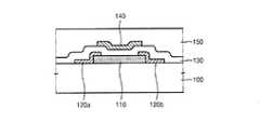
図1は、本発明の実施例1による薄膜トランジスタ(以下、本発明の第1薄膜トランジスタ)を示している。本発明の第1薄膜トランジスタは、ゲート電極140がチャンネル層110上に形成されるトップゲート構造である。 FIG. 1 shows a thin film transistor (hereinafter referred to as a first thin film transistor of the present invention) according to Example 1 of the present invention. The first thin film transistor of the present invention has a top gate structure in which the
図1を参照すれば、基板100上にチャンネル層110が形成されている。基板100は、シリコン基板、ガラス基板及びプラスチック基板のうちの一つであって、透明又は不透明であり得る。基板100上に、ソース電極120a及びドレイン電極120bがチャンネル層110の両端にそれぞれ接触するように形成されている。ソース電極120a及びドレイン電極120bは、単一金属層又は多重金属層であり得る。基板100上に、チャンネル層110、ソース電極120a及びドレイン電極120bを覆うゲート絶縁層130が形成されている。ゲート絶縁層130上に、ゲート電極140が形成されている。ゲート電極140は、チャンネル層110上に位置する。ゲート電極140は、ソース電極120aと同じ金属であるが、他の金属でもあり得る。ゲート絶縁層130上に、ゲート電極140を覆う保護層150が形成されている。ゲート絶縁層130及び保護層150は、シリコン酸化物層又はシリコン窒化物層であり得る。 Referring to FIG. 1, a
一方、チャンネル層110、ソース電極120a、ドレイン電極120b、ゲート絶縁層130及びゲート電極140の厚さは、それぞれ30〜200nm、10〜200nm、10〜200nm、50〜300nm及び100〜300nmほどであり得る。 Meanwhile, the thicknesses of the
チャンネル層110は、遷移金属のドーピングされたIZO(Indium Zinc Oxide)層である。IZO層は、a(In2O3)・b(ZnO)層であり得る。ここで、a及びbは、それぞれa>0及びb>0の条件を満足する実数であるが、0<a≦1及びb≧1の条件を満足する実数であることが望ましい。遷移金属は、9〜11族元素(Co、Rh、Ir、Mt、Ni、Pd、Pt、Ds、Cu、Ag、Au、Rg)のうちの少なくともいずれか一つであり得る。例えば、遷移金属は、Ni又はCuであり得る。遷移金属のドーピング濃度は、103〜1022atom/cm3であることが望ましい。The
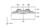
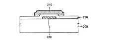
図2は、本発明の実施例2による薄膜トランジスタ(以下、本発明の第2薄膜トランジスタ)を示している。本発明の第2薄膜トランジスタは、ゲート電極240がチャンネル層210の下に形成されるボトムゲート構造である。 FIG. 2 shows a thin film transistor (hereinafter referred to as a second thin film transistor of the present invention) according to Example 2 of the present invention. The second thin film transistor of the present invention has a bottom gate structure in which the
図2を参照すれば、基板200上にゲート電極240が形成されており、基板200上に、ゲート電極240を覆うゲート絶縁層230が形成されている。ゲート電極240の上側のゲート絶縁層230上に、チャンネル層210が形成されている。チャンネル層210は、遷移金属のドーピングされたIZO層であり得る。チャンネル層210のX軸方向の幅は、ゲート電極240のX軸方向の幅より大きくあり得る。ゲート絶縁層230上に、ソース電極220a及びドレイン電極220bがチャンネル層210の両端にそれぞれ接触するように形成されている。ゲート絶縁層230上に、チャンネル層210、ソース電極220a及びドレイン電極220bを覆う保護層250が形成されている。図2の基板200、チャンネル層210、ソース電極220a、ドレイン電極220b、ゲート絶縁層230、ゲート電極240、保護層250それぞれの材質及び厚さは、図1の基板100、チャンネル層110、ソース電極120a、ドレイン電極120b、ゲート絶縁層130、ゲート電極140、保護層150それぞれのそれらと同一であり得る。 Referring to FIG. 2, a
図3乃至図8は、本発明の実施例1による薄膜トランジスタの製造方法(以下、本発明の第1方法)を示している。図1と図3乃至図8とで同じ図面符号は、同じ構成要素を示す。 3 to 8 show a method of manufacturing a thin film transistor (hereinafter referred to as a first method of the present invention) according to the first embodiment of the present invention. The same reference numerals in FIG. 1 and FIGS. 3 to 8 denote the same components.
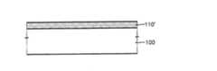
図3を参照すれば、基板100上に、チャンネル用の半導体物質層110’を形成する。半導体物質層110’は、遷移金属のドーピングされたIZO層であり得る。遷移金属は、9〜11族元素のうちの少なくともいずれか一つであり得る。遷移金属のドーピング濃度は、103〜1022atom/cm3であることが望ましい。半導体物質層110’は、スパッタリング法又は蒸発(evaporation)法のような物理気相蒸着(PVD:Physical Vapor Deposition)法で形成できる。半導体物質層110’の形成に1個以上のターゲットが使われ、遷移金属は、ターゲットに含まれていることが可能である。例えば、1個以上のターゲットは、In2O3及びGa2O3のうちの少なくとも一つと、遷移金属とを含むことができる。もしターゲットが遷移金属を含まないならば、基板100上に未ドーピングIZO層が形成されるが、その場合、未ドーピングIZO層に遷移金属イオンを注入(implantation)することにより、半導体物質層110’を形成できる。従って、半導体物質層110’は、遷移金属のドーピングされたa(In2O3)・b(ZnO)層であり得る。ここで、a及びbは、それぞれa>0及びb>0の条件を満足する実数であるが、0<a≦1及びb≧1の条件を満足する実数であることが望ましい。Referring to FIG. 3, a
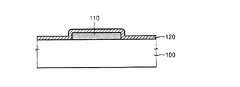
図4を参照すれば、半導体物質層110’をパターニングしてチャンネル層110を形成する。 Referring to FIG. 4, the
図5を参照すれば、基板100上に、チャンネル層110を覆うソース/ドレイン電極層120を形成する。ソース/ドレイン電極層120は、単一金属層又は多重金属層によって形成できる。 Referring to FIG. 5, a source /
図6を参照すれば、ソース/ドレイン電極層120を所定の方法、例えばドライエッチング法によってパターニングし、チャンネル層110の上部ならば一部を露出させ、チャンネル層110両端にそれぞれ接触されたソース電極120a及びドレイン電極120bを形成する。 Referring to FIG. 6, the source /
図7を参照すれば、基板100上に、チャンネル層110の露出した部分とソース電極120a及びドレイン電極120bとを覆うゲート絶縁層130を形成する。ゲート絶縁層130は、シリコン酸化物又はシリコン窒化物によって形成できる。次に、ゲート絶縁層130上に、ゲート電極140を形成する。ゲート電極140は、チャンネル層110上に位置するように形成する。ゲート電極140は、ソース/ドレイン電極層120と同じ金属又は異なる金属によって形成できる。 Referring to FIG. 7, a
図8を参照すれば、ゲート絶縁層130上に、ゲート電極140を覆うように保護層150を形成する。保護層150は、シリコン酸化物又はシリコン窒化物によって形成できる。このような方法によって形成された薄膜トランジスタは、所定温度でアニーリング可能である。 Referring to FIG. 8, the
図9乃至図12は、本発明の実施例2による薄膜トランジスタの製造方法(以下、本発明の第2方法)を示している。本発明の第2方法は、ボトムゲート構造の薄膜トランジスタの製造方法である。図2と図9乃至図12とで同じ図面符号は、同じ構成要素を示す。 9 to 12 show a method of manufacturing a thin film transistor according to the second embodiment of the present invention (hereinafter, the second method of the present invention). The second method of the present invention is a method of manufacturing a bottom gate thin film transistor. The same reference numerals in FIG. 2 and FIGS. 9 to 12 denote the same components.
図9を参照すれば、基板200上にゲート電極240を形成し、基板200上にゲート電極240を覆うゲート絶縁層230を形成する。 Referring to FIG. 9, the
図10を参照すれば、ゲート絶縁層230上にチャンネル層210を形成する。このとき、チャンネル層210は、ゲート電極240上に位置するように形成する。ここで、チャンネル層210は、図3及び図4を参照して説明したチャンネル層110の形成方法と同じ方法によって形成でき、図2のチャンネル層210と等価であり得る。 Referring to FIG. 10, the
図11を参照すれば、ゲート絶縁層230上に、チャンネル層210の両端にそれぞれ接触してチャンネル層210の上部面の一部を露出させるソース電極220a及びドレイン電極220bを形成する。 Referring to FIG. 11, a
図12を参照すれば、基板200上に、チャンネル層210の露出した部分と、ソース電極220a及びドレイン電極220bとを覆う保護層250を形成する。 Referring to FIG. 12, a
図13は、本発明の実施例2によって製造した薄膜トランジスタのドレイン電圧Vd別のゲート電圧Vg−ドレイン電流Idの特性を示している。図13は、NiのドーピングされたIZO層をチャンネル層210として使用した薄膜トランジスタについての結果である。このとき、チャンネル層210で、Zn、In及びNiの含有量比は、Zn:In:Ni=1:1.0121:0.0079(atomic ratio)ほどである。 FIG. 13 shows the characteristics of gate voltage Vg−drain current Id for each drain voltage Vd of the thin film transistor manufactured according to Example 2 of the present invention. FIG. 13 shows the results for a thin film transistor using a Ni-doped IZO layer as the
図14は、本発明の実施例との比較のための比較例によって製造した薄膜トランジスタのドレイン電圧Vd別のゲート電圧Vg−ドレイン電流Idの特性を示している。図14は、未ドーピングIZO層をチャンネル層として使用した薄膜トランジスタについての結果である。比較例によって製造した薄膜トランジスタで、チャンネル層の材質を除外した残りの構成は、図2のそれと同一である。 FIG. 14 shows characteristics of gate voltage Vg-drain current Id for each drain voltage Vd of a thin film transistor manufactured by a comparative example for comparison with the embodiment of the present invention. FIG. 14 shows the results for the thin film transistor using the undoped IZO layer as the channel layer. In the thin film transistor manufactured according to the comparative example, the remaining configuration excluding the material of the channel layer is the same as that of FIG.
図13及び図14を参照すれば、本発明による薄膜トランジスタは、10.1Vほどの高いVdでもすぐれたスイッチング特性を示す一方、比較例による薄膜トランジスタは、0.1Vほどの低いVdでもスイッチング特性が示されないということが分かる。このような結果は、本発明の薄膜トランジスタのチャンネル層210にドーピングされた遷移金属がチャンネル層210の電気伝導度を適切に調節するためである。更に具体的に説明すれば、比較例による薄膜トランジスタのチャンネル層は、4個の原子価原子を有するInを含み、遷移金属を含まない。このような比較例のチャンネル層は、過度に大きい電気伝導度を有し、注目すべきゲート電圧範囲でスイッチング特性を示さない。一方、本発明による薄膜トランジスタのチャンネル層210は、4つ未満の原子価電子を有する遷移金属を含むために、スイッチングのための適切な電気伝導度を有しうる。また、比較例のチャンネル層、すなわち未ドーピングIZO層は、光に非常に敏感に反応するために、表示装置のチャンネル層として適用するのに不適であるが、遷移金属のドーピングされたチャンネル層110、210は、光に対して安定的であるゆえに、表示装置のチャンネル層として適用するのに適している。 Referring to FIGS. 13 and 14, the thin film transistor according to the present invention exhibits excellent switching characteristics even at Vd as high as 10.1V, while the thin film transistor according to the comparative example exhibits switching characteristics even at Vd as low as 0.1V. I understand that it is not done. This is because the transition metal doped in the
併せて、図13の結果から、本発明による薄膜トランジスタのオン(ON)電流とオフ(OFF)電流との比(ON/OFF current ratio)は、106ほどと高いことが分かる。また、本発明の薄膜トランジスタは、30cm2/Vsほどの高い移動度を有する。従って、本発明の薄膜トランジスタは、優秀なスイッチング特性を示すことができる。In addition, it can be seen from the results of FIG. 13 that the ratio (ON / OFF current ratio) of the thin film transistor according to the present invention is as high as 106 . The thin film transistor of the present invention has a high mobility of about 30 cm2 / Vs. Therefore, the thin film transistor of the present invention can exhibit excellent switching characteristics.
上記の説明で多くの事項が具体的に記載されているが、それらは、発明の範囲を限定するものと見るより、望ましい実施形態の例示として解釈されねばならない。例えば、本発明の属する技術分野で当業者ならば、薄膜トランジスタの構成要素及び構造は、それぞれ多様化されて変形され得るということが分かる。また、薄膜トランジスタは、液晶表示装置や有機発光表示装置の分野だけではなく、メモリ素子及び論理素子の分野などにも適用され得るということが分かる。よって、本発明は、上述の実施形態に限られるものではなく、本発明の技術的範囲から逸脱しない範囲内で多様に変更実施することが可能である。 Although many items have been specifically described in the above description, they should be construed as examples of preferred embodiments rather than as limiting the scope of the invention. For example, those skilled in the art to which the present invention pertains can understand that the components and structure of the thin film transistor can be varied and modified. Further, it can be seen that the thin film transistor can be applied not only to the fields of liquid crystal display devices and organic light emitting display devices, but also to the fields of memory elements and logic elements. Therefore, the present invention is not limited to the above-described embodiment, and various modifications can be made without departing from the technical scope of the present invention.
本発明のチャンネル層とその形成方法、及び該チャンネル層を含む薄膜トランジスタとその製造方法は、例えば、スイッチング素子関連の技術分野に効果的に適用可能である。 The channel layer and the method for forming the same according to the present invention, and the thin film transistor including the channel layer and the method for manufacturing the thin film transistor can be effectively applied to, for example, the technical field related to switching elements.
100、200 基板
110、210 チャンネル層
110’ 半導体物質層
120 ソース/ドレイン電極層
120a、220a ソース電極
120b、220b ドレイン電極
130、230 ゲート絶縁層
140、240 ゲート電極
150、250 保護層100, 200
Claims (25)
Translated fromJapanese遷移金属のドーピングされたIZOを含むことを特徴とするチャンネル層。A channel layer used for a thin film transistor,
A channel layer comprising a transition metal doped IZO.
前記ゲート電極と前記チャンネル層との間に備わるゲート絶縁層と、
前記チャンネル層の両端にそれぞれ接触するソース電極及びドレイン電極と、を備えることを特徴とする薄膜トランジスタ。A gate electrode provided on a substrate and the channel layer according to claim 1;
A gate insulating layer provided between the gate electrode and the channel layer;
A thin film transistor comprising: a source electrode and a drain electrode that are in contact with both ends of the channel layer, respectively.
チャンネル形成のための半導体物質層を設ける段階と、
前記半導体物質層をパターニングしてチャンネル層を形成する段階と、を有し、
前記半導体物質層は、遷移金属のドーピングされたIZOを含むことを特徴とするチャンネル層の形成方法。A method of forming a channel layer used in a thin film transistor,
Providing a semiconductor material layer for channel formation;
Patterning the semiconductor material layer to form a channel layer,
The method for forming a channel layer, wherein the semiconductor material layer includes IZO doped with a transition metal.
前記チャンネル層の両端にそれぞれ接触するソース電極及びドレイン電極を形成する段階と、
前記チャンネル層の露出部、前記ソース電極及び前記ドレイン電極上にゲート絶縁層を形成する段階と、
前記ゲート絶縁層上にゲート電極を形成する段階と、を有することを特徴とする薄膜トランジスタの製造方法。Forming a channel layer according to claim 14 on a substrate;
Forming a source electrode and a drain electrode respectively in contact with both ends of the channel layer;
Forming a gate insulating layer on the exposed portion of the channel layer, the source electrode and the drain electrode;
Forming a gate electrode on the gate insulating layer. A method of manufacturing a thin film transistor, comprising:
前記ゲート絶縁層上に請求項14に記載のチャンネル層を形成する段階と、
前記チャンネル層の両端にそれぞれ接触するソース電極及びドレイン電極を形成する段階と、を有することを特徴とする薄膜トランジスタの製造方法。Forming a gate electrode and a gate insulating layer on the substrate in order;
Forming a channel layer according to claim 14 on the gate insulating layer;
Forming a source electrode and a drain electrode in contact with both ends of the channel layer, respectively.
Applications Claiming Priority (1)
| Application Number | Priority Date | Filing Date | Title |
|---|---|---|---|
| KR1020070063826AKR101344483B1 (en) | 2007-06-27 | 2007-06-27 | Thin film transistor |
Publications (1)
| Publication Number | Publication Date |
|---|---|
| JP2009010348Atrue JP2009010348A (en) | 2009-01-15 |
Family
ID=40159323
Family Applications (1)
| Application Number | Title | Priority Date | Filing Date |
|---|---|---|---|
| JP2008131631APendingJP2009010348A (en) | 2007-06-27 | 2008-05-20 | Channel layer and method for forming the same, thin film transistor including the channel layer, and method for manufacturing the same |
Country Status (4)
| Country | Link |
|---|---|
| US (1) | US8324628B2 (en) |
| JP (1) | JP2009010348A (en) |
| KR (1) | KR101344483B1 (en) |
| CN (1) | CN101335301B (en) |
Cited By (5)
| Publication number | Priority date | Publication date | Assignee | Title |
|---|---|---|---|---|
| JP2011119675A (en)* | 2009-10-30 | 2011-06-16 | Semiconductor Energy Lab Co Ltd | Semiconductor device |
| JP2011129888A (en)* | 2009-11-06 | 2011-06-30 | Semiconductor Energy Lab Co Ltd | Semiconductor device |
| JP2012256399A (en)* | 2010-08-06 | 2012-12-27 | Semiconductor Energy Lab Co Ltd | Semiconductor device and method for driving the same |
| KR101728943B1 (en) | 2015-04-24 | 2017-04-20 | 경희대학교 산학협력단 | Sensor for recognizing touch |
| US10890761B2 (en) | 2015-04-24 | 2021-01-12 | University-Industry Cooperation Group Of Kyung Hee University | Photoreactive sensor including optical amplification phototransistor, and display panel and vehicle control system including photoreactive sensor |
Families Citing this family (9)
| Publication number | Priority date | Publication date | Assignee | Title |
|---|---|---|---|---|
| CN104157694A (en)* | 2009-09-30 | 2014-11-19 | 大日本印刷株式会社 | Substrate for flexible device, flexible device, thin film transistor and method for manufacturing same |
| CN104332177B (en) | 2009-11-20 | 2018-05-08 | 株式会社半导体能源研究所 | Non-volatile latch circuit and logic circuit, and use its semiconductor devices |
| EP2348531B1 (en)* | 2010-01-26 | 2021-05-26 | Samsung Electronics Co., Ltd. | Thin film transistor and method of manufacturing the same |
| CN103828061B (en)* | 2011-10-07 | 2018-02-13 | 应用材料公司 | Carry out the method for deposit silicon-containing materials using argon-dilution |
| US9312257B2 (en)* | 2012-02-29 | 2016-04-12 | Semiconductor Energy Laboratory Co., Ltd. | Semiconductor device |
| JP6051960B2 (en)* | 2012-03-19 | 2016-12-27 | 株式会社リコー | Conductive thin film, coating liquid for forming conductive thin film, field effect transistor, and method of manufacturing field effect transistor |
| JP6516978B2 (en) | 2013-07-17 | 2019-05-22 | 株式会社半導体エネルギー研究所 | Semiconductor device |
| CN105514211B (en)* | 2015-12-18 | 2017-08-25 | 河南大学 | A kind of transparent field effect ultraviolet detector of grid voltage control and preparation method thereof |
| US11710775B2 (en)* | 2020-05-29 | 2023-07-25 | Taiwan Semiconductor Manufacturing Co., Ltd. | Ferroelectric field effect transistor |
Citations (3)
| Publication number | Priority date | Publication date | Assignee | Title |
|---|---|---|---|---|
| JP2006165528A (en)* | 2004-11-10 | 2006-06-22 | Canon Inc | Image display device |
| JP2006165529A (en)* | 2004-11-10 | 2006-06-22 | Canon Inc | Amorphous oxide and field effect transistor |
| JP2007073703A (en)* | 2005-09-06 | 2007-03-22 | Canon Inc | Thin film transistor and thin film diode |
Family Cites Families (8)
| Publication number | Priority date | Publication date | Assignee | Title |
|---|---|---|---|---|
| JP4089858B2 (en) | 2000-09-01 | 2008-05-28 | 国立大学法人東北大学 | Semiconductor device |
| JP4090716B2 (en)* | 2001-09-10 | 2008-05-28 | 雅司 川崎 | Thin film transistor and matrix display device |
| JP4164562B2 (en) | 2002-09-11 | 2008-10-15 | 独立行政法人科学技術振興機構 | Transparent thin film field effect transistor using homologous thin film as active layer |
| JP2004193446A (en) | 2002-12-13 | 2004-07-08 | Sanyo Electric Co Ltd | Method for manufacturing semiconductor device and method for manufacturing thin film transistor |
| JP2004235180A (en) | 2003-01-28 | 2004-08-19 | Sanyo Electric Co Ltd | Semiconductor device and manufacturing method thereof |
| US7262463B2 (en)* | 2003-07-25 | 2007-08-28 | Hewlett-Packard Development Company, L.P. | Transistor including a deposited channel region having a doped portion |
| TWI221341B (en)* | 2003-09-18 | 2004-09-21 | Ind Tech Res Inst | Method and material for forming active layer of thin film transistor |
| US7145174B2 (en) | 2004-03-12 | 2006-12-05 | Hewlett-Packard Development Company, Lp. | Semiconductor device |
- 2007
- 2007-06-27KRKR1020070063826Apatent/KR101344483B1/ennot_activeExpired - Fee Related
- 2008
- 2008-02-29USUS12/073,102patent/US8324628B2/ennot_activeExpired - Fee Related
- 2008-03-31CNCN2008100886159Apatent/CN101335301B/ennot_activeExpired - Fee Related
- 2008-05-20JPJP2008131631Apatent/JP2009010348A/enactivePending
Patent Citations (3)
| Publication number | Priority date | Publication date | Assignee | Title |
|---|---|---|---|---|
| JP2006165528A (en)* | 2004-11-10 | 2006-06-22 | Canon Inc | Image display device |
| JP2006165529A (en)* | 2004-11-10 | 2006-06-22 | Canon Inc | Amorphous oxide and field effect transistor |
| JP2007073703A (en)* | 2005-09-06 | 2007-03-22 | Canon Inc | Thin film transistor and thin film diode |
Cited By (19)
| Publication number | Priority date | Publication date | Assignee | Title |
|---|---|---|---|---|
| US10510757B2 (en) | 2009-10-30 | 2019-12-17 | Semiconductor Energy Laboratory Co., Ltd. | Semiconductor device including storage element |
| US9685447B2 (en) | 2009-10-30 | 2017-06-20 | Semiconductor Energy Laboratory Co., Ltd. | Semiconductor device comprising transistor including oxide semiconductor |
| US12211534B2 (en) | 2009-10-30 | 2025-01-28 | Semiconductor Energy Laboratory Co., Ltd. | Semiconductor device |
| US12205622B2 (en) | 2009-10-30 | 2025-01-21 | Semiconductor Energy Laboratory Co., Ltd. | Semiconductor device |
| US11963374B2 (en) | 2009-10-30 | 2024-04-16 | Semiconductor Energy Laboratory Co., Ltd. | Semiconductor device |
| US9105511B2 (en) | 2009-10-30 | 2015-08-11 | Semiconductor Energy Laboratory Co., Ltd. | Semiconductor device comprising oxide semiconductor |
| US9373640B2 (en) | 2009-10-30 | 2016-06-21 | Semiconductor Energy Laboratory Co., Ltd. | Semiconductor device |
| US11322498B2 (en) | 2009-10-30 | 2022-05-03 | Semiconductor Energy Laboratory Co., Ltd. | Semiconductor device |
| US10811417B2 (en) | 2009-10-30 | 2020-10-20 | Semiconductor Energy Laboratory Co., Ltd. | Semiconductor device |
| TWI574388B (en)* | 2009-10-30 | 2017-03-11 | 半導體能源研究所股份有限公司 | Semiconductor device |
| US8896042B2 (en) | 2009-10-30 | 2014-11-25 | Semiconductor Energy Laboratory Co., Ltd. | Semiconductor device comprising oxide semiconductor |
| JP2011119675A (en)* | 2009-10-30 | 2011-06-16 | Semiconductor Energy Lab Co Ltd | Semiconductor device |
| US10056385B2 (en) | 2009-11-06 | 2018-08-21 | Semiconductor Energy Laboratory Co., Ltd. | Semiconductor device including write access transistor whose oxide semiconductor layer including channel formation region |
| JP2011129888A (en)* | 2009-11-06 | 2011-06-30 | Semiconductor Energy Lab Co Ltd | Semiconductor device |
| US9589961B2 (en) | 2009-11-06 | 2017-03-07 | Semiconductor Energy Laboratory Co., Ltd. | Semiconductor device including write access transistor having channel region including oxide semiconductor |
| US9001566B2 (en) | 2009-11-06 | 2015-04-07 | Semiconductor Energy Laboratory Co., Ltd. | Method for driving semiconductor device |
| JP2012256399A (en)* | 2010-08-06 | 2012-12-27 | Semiconductor Energy Lab Co Ltd | Semiconductor device and method for driving the same |
| US10890761B2 (en) | 2015-04-24 | 2021-01-12 | University-Industry Cooperation Group Of Kyung Hee University | Photoreactive sensor including optical amplification phototransistor, and display panel and vehicle control system including photoreactive sensor |
| KR101728943B1 (en) | 2015-04-24 | 2017-04-20 | 경희대학교 산학협력단 | Sensor for recognizing touch |
Also Published As
| Publication number | Publication date |
|---|---|
| CN101335301A (en) | 2008-12-31 |
| CN101335301B (en) | 2013-09-18 |
| US8324628B2 (en) | 2012-12-04 |
| KR20080114357A (en) | 2008-12-31 |
| US20090001432A1 (en) | 2009-01-01 |
| KR101344483B1 (en) | 2013-12-24 |
Similar Documents
| Publication | Publication Date | Title |
|---|---|---|
| JP2009010348A (en) | Channel layer and method for forming the same, thin film transistor including the channel layer, and method for manufacturing the same | |
| CN101304046B (en) | Thin film transistor and method for forming the same | |
| JP5536328B2 (en) | Transistor and manufacturing method thereof | |
| CN101661952B (en) | Amorphous oxide semiconductor and thin film transistor using same | |
| US8466462B2 (en) | Thin film transistor and method of fabricating the same | |
| KR101413655B1 (en) | Method for manufacturing oxide semiconductor thin film transistor | |
| US20120025187A1 (en) | Transistors, methods of manufacturing transistors, and electronic devices including transistors | |
| CN102136499B (en) | Thin-film transistor and manufacture method thereof | |
| US9048163B2 (en) | Transistor, electronic device including transistor, and manufacturing methods thereof | |
| KR101238823B1 (en) | The thin film transistor and the manufacuring method thereof | |
| KR20090119666A (en) | Semiconductor device and manufacturing method | |
| JP2011071476A (en) | Thin film transistor, display device using the same, and method of manufacturing thin film transistor | |
| TW200937534A (en) | Method for manufacturing field-effect transistor | |
| JP2010016126A (en) | Thin film field effect transistor, fabrication process therefor, and display device using the same | |
| CN104885189A (en) | Metal oxide tft with improved temperature stability | |
| KR20150030518A (en) | Thin film transistor and manufacturing method thereof | |
| JP6260326B2 (en) | Thin film transistor device and manufacturing method thereof | |
| KR102231372B1 (en) | Metal oxide thin film transistor and preparation method thereof | |
| KR20110080118A (en) | A thin film transistor having a multilayer etch stop layer and a method of manufacturing the same | |
| KR101088366B1 (en) | Thin film transistor having buried layer and manufacturing method thereof | |
| KR102537352B1 (en) | Thin film trnasistor having doped oxide semiconductor layer, method for manufacturing the same and display device comprising the same | |
| KR102849626B1 (en) | CMOS thin film inverter device having oxide semiconductor and method of fabricating the same | |
| KR102571072B1 (en) | Thin Film Transistor and Preparation Method Thereof | |
| KR101303428B1 (en) | Oxide thin film transistor and thereof |
Legal Events
| Date | Code | Title | Description |
|---|---|---|---|
| A621 | Written request for application examination | Free format text:JAPANESE INTERMEDIATE CODE: A621 Effective date:20110511 | |
| A521 | Request for written amendment filed | Free format text:JAPANESE INTERMEDIATE CODE: A523 Effective date:20120426 | |
| A977 | Report on retrieval | Free format text:JAPANESE INTERMEDIATE CODE: A971007 Effective date:20130215 | |
| A131 | Notification of reasons for refusal | Free format text:JAPANESE INTERMEDIATE CODE: A131 Effective date:20130219 | |
| A521 | Request for written amendment filed | Free format text:JAPANESE INTERMEDIATE CODE: A523 Effective date:20130517 | |
| A02 | Decision of refusal | Free format text:JAPANESE INTERMEDIATE CODE: A02 Effective date:20130702 |