JP2009010105A - Wafer laser processing method - Google Patents
Wafer laser processing methodDownload PDFInfo
- Publication number
- JP2009010105A JP2009010105AJP2007168933AJP2007168933AJP2009010105AJP 2009010105 AJP2009010105 AJP 2009010105AJP 2007168933 AJP2007168933 AJP 2007168933AJP 2007168933 AJP2007168933 AJP 2007168933AJP 2009010105 AJP2009010105 AJP 2009010105A
- Authority
- JP
- Japan
- Prior art keywords
- laser beam
- wafer
- layer
- crack
- layers
- Prior art date
- Legal status (The legal status is an assumption and is not a legal conclusion. Google has not performed a legal analysis and makes no representation as to the accuracy of the status listed.)
- Granted
Links
Images


Classifications
- H—ELECTRICITY
- H01—ELECTRIC ELEMENTS
- H01L—SEMICONDUCTOR DEVICES NOT COVERED BY CLASS H10
- H01L21/00—Processes or apparatus adapted for the manufacture or treatment of semiconductor or solid state devices or of parts thereof
- H01L21/70—Manufacture or treatment of devices consisting of a plurality of solid state components formed in or on a common substrate or of parts thereof; Manufacture of integrated circuit devices or of parts thereof
- H01L21/77—Manufacture or treatment of devices consisting of a plurality of solid state components or integrated circuits formed in, or on, a common substrate
- H01L21/78—Manufacture or treatment of devices consisting of a plurality of solid state components or integrated circuits formed in, or on, a common substrate with subsequent division of the substrate into plural individual devices
- B—PERFORMING OPERATIONS; TRANSPORTING
- B23—MACHINE TOOLS; METAL-WORKING NOT OTHERWISE PROVIDED FOR
- B23K—SOLDERING OR UNSOLDERING; WELDING; CLADDING OR PLATING BY SOLDERING OR WELDING; CUTTING BY APPLYING HEAT LOCALLY, e.g. FLAME CUTTING; WORKING BY LASER BEAM
- B23K26/00—Working by laser beam, e.g. welding, cutting or boring
- B23K26/36—Removing material
- B23K26/40—Removing material taking account of the properties of the material involved
- B—PERFORMING OPERATIONS; TRANSPORTING
- B23—MACHINE TOOLS; METAL-WORKING NOT OTHERWISE PROVIDED FOR
- B23K—SOLDERING OR UNSOLDERING; WELDING; CLADDING OR PLATING BY SOLDERING OR WELDING; CUTTING BY APPLYING HEAT LOCALLY, e.g. FLAME CUTTING; WORKING BY LASER BEAM
- B23K26/00—Working by laser beam, e.g. welding, cutting or boring
- B23K26/50—Working by transmitting the laser beam through or within the workpiece
- B23K26/53—Working by transmitting the laser beam through or within the workpiece for modifying or reforming the material inside the workpiece, e.g. for producing break initiation cracks
- B—PERFORMING OPERATIONS; TRANSPORTING
- B28—WORKING CEMENT, CLAY, OR STONE
- B28D—WORKING STONE OR STONE-LIKE MATERIALS
- B28D5/00—Fine working of gems, jewels, crystals, e.g. of semiconductor material; apparatus or devices therefor
- B28D5/0005—Fine working of gems, jewels, crystals, e.g. of semiconductor material; apparatus or devices therefor by breaking, e.g. dicing
- B28D5/0011—Fine working of gems, jewels, crystals, e.g. of semiconductor material; apparatus or devices therefor by breaking, e.g. dicing with preliminary treatment, e.g. weakening by scoring
- B—PERFORMING OPERATIONS; TRANSPORTING
- B23—MACHINE TOOLS; METAL-WORKING NOT OTHERWISE PROVIDED FOR
- B23K—SOLDERING OR UNSOLDERING; WELDING; CLADDING OR PLATING BY SOLDERING OR WELDING; CUTTING BY APPLYING HEAT LOCALLY, e.g. FLAME CUTTING; WORKING BY LASER BEAM
- B23K2103/00—Materials to be soldered, welded or cut
- B23K2103/50—Inorganic material, e.g. metals, not provided for in B23K2103/02 – B23K2103/26
Landscapes
- Engineering & Computer Science (AREA)
- Physics & Mathematics (AREA)
- Optics & Photonics (AREA)
- Mechanical Engineering (AREA)
- Plasma & Fusion (AREA)
- Manufacturing & Machinery (AREA)
- Microelectronics & Electronic Packaging (AREA)
- Power Engineering (AREA)
- Computer Hardware Design (AREA)
- General Physics & Mathematics (AREA)
- Condensed Matter Physics & Semiconductors (AREA)
- Chemical & Material Sciences (AREA)
- Chemical Kinetics & Catalysis (AREA)
- General Chemical & Material Sciences (AREA)
- Oil, Petroleum & Natural Gas (AREA)
- Laser Beam Processing (AREA)
- Dicing (AREA)
- Processing Of Stones Or Stones Resemblance Materials (AREA)
Abstract
Translated fromJapaneseDescription
Translated fromJapanese本発明は、半導体ウェーハ等のウェーハに形成された分割予定ラインに沿ってレーザ光線を照射し、ウェーハの内部に分割予定ラインに沿って変質層を形成するレーザ加工方法に関する。 The present invention relates to a laser processing method for irradiating a laser beam along a predetermined division line formed on a wafer such as a semiconductor wafer and forming a deteriorated layer along the predetermined division line inside the wafer.
半導体デバイスのチップ製造工程においては、略円盤状の半導体ウェーハの表面に、格子状に配列された分割予定ラインによって複数の矩形状の領域を区画し、これら矩形領域にICやLSI等の電子回路や、MEMS(Micro Electro Mechanical System)と呼ばれる微小電気機械素子を形成した後、ウェーハを分割予定ラインに沿って切断して、矩形領域を半導体チップとして得ている。ウェーハの厚さは、600〜800μm程度が一般的であり、この厚さから、必要に応じて裏面研削して薄化加工される場合もあるが、用途によっては薄化されずに、その程度の厚さの状態でウェーハを分割する場合もある。 In the semiconductor device chip manufacturing process, a plurality of rectangular areas are defined on the surface of a substantially disk-shaped semiconductor wafer by dividing lines arranged in a lattice pattern, and electronic circuits such as ICs and LSIs are formed in these rectangular areas. Alternatively, after forming a microelectromechanical element called MEMS (Micro Electro Mechanical System), the wafer is cut along a division line to obtain a rectangular region as a semiconductor chip. The thickness of the wafer is generally about 600 to 800 μm, and from this thickness, it may be thinned by grinding the back surface as necessary, but it is not thinned depending on the application. In some cases, the wafer is divided in the thickness state.
ウェーハを切断する手段としては、高速回転させた薄い円盤状のブレードをウェーハに切り込ませるダイシング法が一般的である。このダイシング法は、平坦かつシャープな切断面が得られるなどの利点があるが、チップ間の分割予定ラインの幅が、用いるブレードの厚さ(主に10〜30μm程度)相当以上の寸法を必要とするため、切断代が比較的大きく、ウェーハ1枚当たりのチップ個数をなるべく多く得て生産性を向上させる面では不利である。 As a means for cutting the wafer, a dicing method is generally used in which a thin disk-shaped blade rotated at a high speed is cut into the wafer. This dicing method has an advantage that a flat and sharp cut surface can be obtained. However, the width of the line to be divided between chips needs to be larger than the thickness of the blade to be used (mainly about 10 to 30 μm). Therefore, the cutting allowance is relatively large, which is disadvantageous in terms of improving the productivity by obtaining as many chips as possible per wafer.
一方、近年では、透過性のレーザ光線を分割予定ラインに沿ってウェーハ内部に照射して物理的強度が低下した変質層を形成し、次いでウェーハに外力を与えることにより、分割予定ラインに沿ってウェーハが割断され、個片化したチップを得るといったレーザ法も採用されてきている。このレーザ法では、切断代がダイシング法と比較すると格段に小さく、生産性の面では有利とされている。ところが、上記のように薄化されることなく比較的厚い状態のままのウェーハをレーザ法で分割するにあたり、1本の分割予定ラインについてレーザ光線を1回照射して変質層を一層形成しても、厚さに比して変質層の割合が小さく、円滑に分割されない場合がある。 On the other hand, in recent years, a translucent laser beam is irradiated along the planned dividing line to the inside of the wafer to form a deteriorated layer having reduced physical strength, and then an external force is applied to the wafer along the planned dividing line. A laser method has also been adopted in which a wafer is cleaved to obtain individual chips. In this laser method, the cutting allowance is much smaller than that in the dicing method, which is advantageous in terms of productivity. However, when a wafer that has remained relatively thin without being thinned as described above is divided by the laser method, one layer of a deteriorated layer is formed by irradiating a laser beam once on one division planned line. However, the proportion of the deteriorated layer is small compared to the thickness, and may not be divided smoothly.
そこで、1本の分割予定ラインについてレーザ光線を複数段階に照射して多層の変質層を形成し、割断を容易、かつ精密に実施可能とした技術が知られている(特許文献1参照)。また、照射するレーザ光線の波長を、従来の1064nmから、ウェーハ内部への透過性がより良好な1100〜2000nm(好ましくは1300〜1600nm)に変えることにより、変質層を効率よく形成する技術も提案されている。 In view of this, a technique is known in which a laser beam is irradiated to a plurality of stages on a single division line to form a multi-layered altered layer so that cleaving can be performed easily and precisely (see Patent Document 1). Also proposed is a technique for efficiently forming a deteriorated layer by changing the wavelength of the laser beam to be irradiated from the conventional 1064 nm to 1100 to 2000 nm (preferably 1300 to 1600 nm) with better transparency into the wafer. Has been.
例えば、625μmの厚さのウェーハにレーザ光線を照射して割断する場合には、従来の1064nm波長のレーザ光線では、ウェーハの厚さ方向に概ね18層程度の多層な変質層が必要である。これはすなわち、レーザ光線照射を1本の分割予定ラインについて18回行うことになり、照射回数が多くて加工効率がよいとは言えない。一方、1342nm波長のレーザ光線を使用すれば変質層は8層程度で割断が可能であり、加工効率は改善される。ところが1342nm波長のレーザ光線を照射しても、多層の変質層を厚さ方向に近接して形成することは、実際には困難である。多層の変質層を形成した場合、形成された変質層から、隣接する変質層に向かってクラック層が延びて到達した状態となることにより、円滑な割断が実現できるとされている。したがって多層の変質層を近接して形成することができないと、隣接する変質層へのクラック層の到達が起こりにくく、割断不良が起こりやすい。 For example, when a wafer having a thickness of 625 μm is cleaved by irradiating it with a laser beam, a conventional laser beam with a wavelength of 1064 nm requires a multi-layered alteration layer of about 18 layers in the thickness direction of the wafer. In other words, the laser beam irradiation is performed 18 times for one division planned line, and it cannot be said that the processing efficiency is good due to the large number of irradiation times. On the other hand, if a laser beam having a wavelength of 1342 nm is used, the altered layer can be cleaved with about 8 layers, and the processing efficiency is improved. However, even if a laser beam having a wavelength of 1342 nm is irradiated, it is actually difficult to form a multi-layered altered layer close to the thickness direction. When a multi-layered altered layer is formed, it is said that a smooth cleaving can be realized by a crack layer extending from the formed altered layer toward an adjacent altered layer. Therefore, if the multi-layered deteriorated layer cannot be formed close to the cracked layer, it is difficult for the cracked layer to reach the adjacent deteriorated layer, and cleaving failure is likely to occur.
隣接する変質層を近接して形成することが困難な理由としては、一旦形成された変質層と、この変質層から延びるクラック層の近辺では、結晶レベルでの歪みや欠陥層が形成されており、その部分にレーザ光線を照射しても良好に集光されないため多光子吸収が十分になされないからと推測されている。このため、先に形成した第1の変質層に隣接する第2の変質層を形成する場合は、第1の変質層から延びるクラック層からある程度離間させて形成することを余儀なくされ、結果として、第1の変質層から延びるクラック層が第2の変質層に到達していない状態となって、割断不良が起こりやすくなる。 The reason why it is difficult to form adjacent deteriorated layers close to each other is that strains and defect layers at the crystal level are formed in the vicinity of the once formed deteriorated layer and the crack layer extending from this deteriorated layer. It is presumed that the multi-photon absorption is not sufficiently performed because the light is not condensed well even if the portion is irradiated with the laser beam. For this reason, in the case of forming the second deteriorated layer adjacent to the first deteriorated layer formed earlier, it is inevitably formed to be separated from the crack layer extending from the first deteriorated layer to some extent. The crack layer extending from the first deteriorated layer does not reach the second deteriorated layer, so that cleaving defects are likely to occur.
よって本発明は、加工効率を低下させることなく、容易、かつ確実にウェーハを割断することができるウェーハのレーザ加工方法を提供することを目的としている。 Therefore, an object of the present invention is to provide a wafer laser processing method capable of cleaving a wafer easily and reliably without lowering the processing efficiency.
本発明は、レーザ光線を、ウェーハに形成された分割予定ラインに沿って、該ウェーハの一面側からウェーハ内部に照射するレーザ光線照射動作を複数回にわたって行うにあたり、該動作を行う都度、レーザ光線の焦点位置を入射方向に段階的に変化させ、これによってウェーハの内部に、分割予定ラインに沿った複数の変質層を、ウェーハの厚さ方向に複数層形成するウェーハのレーザ加工方法であって、保持台に、ウェーハの他面を合わせ、かつ、一面を露出させて保持するウェーハ保持工程と、上記レーザ光線照射動作を、保持台に保持したウェーハの他面側から一面側にわたって複数回行うことにより、変質層と、該変質層から一面方向に延びるクラック層とからなる複数の複合層を、入射方向に間隔を空けて段階的に形成する第1のレーザ光線照射工程と、第1のレーザ光線照射工程で形成された複数の複合層の間に、レーザ光線の焦点位置を合わせてレーザ光線を照射し、これによってクラック層を一面方向に延伸させて該方向に隣接する変質層に到達させる第2のレーザ光線照射工程とを備えることを特徴としている。 In the present invention, when performing laser beam irradiation operation for irradiating a laser beam to the inside of the wafer from one side of the wafer along a predetermined division line formed on the wafer a plurality of times, each time the operation is performed, the laser beam A wafer laser processing method in which a plurality of deteriorated layers along a planned dividing line are formed in a wafer in a thickness direction by changing a focal position of the wafer stepwise in an incident direction. The wafer holding step of holding the other surface of the wafer on the holding table and exposing one surface, and the laser beam irradiation operation are performed a plurality of times from the other surface side of the wafer held on the holding table to the one surface side. In this way, a plurality of composite layers composed of a deteriorated layer and a crack layer extending in one surface direction from the deteriorated layer are formed stepwise at intervals in the incident direction. The laser beam is irradiated between the plurality of composite layers formed in the laser beam irradiation step and the first laser beam irradiation step so that the focal position of the laser beam is adjusted, thereby extending the crack layer in one surface direction. And a second laser beam irradiation step for reaching a deteriorated layer adjacent in the direction.
本発明によれば、第1のレーザ光線照射工程によってウェーハ内部に形成された複数の複合層(変質層+クラック層)の間には、クラック層が存在していないが、クラック層から延びる結晶欠陥などの影響によりレーザ光線を照射しても多光子吸収はなされず、変質層は形成されにくい。しかし、レーザ光線の照射によってすでに存在する変質層から延びるクラック層を延伸させる作用が見込まれる。第2のレーザ光線照射工程ではこの非クラック層にレーザ光線を照射し、クラック層を隣接する複合層の変質層に延伸させる。これによってクラック層を変質層に到達させることができる。このため、ウェーハの割断を行った際には、その割断を、容易、かつ円滑に行うことができ、割断不良を招くことがない。また、本発明では第2のレーザ光線照射工程を行うことによって、第1のレーザ光線照射工程によって形成する変質層の数を低減することができ、双方の工程によるレーザ光線照射の総回数も、従来の割断可能なレーザ光線照射回数より低減させることができる。このため、加工効率の低下も抑えられる。 According to the present invention, there is no crack layer between the plurality of composite layers (modified layer + crack layer) formed in the wafer by the first laser beam irradiation step, but the crystal extending from the crack layer Even if the laser beam is irradiated due to the influence of defects or the like, multiphoton absorption is not performed, and an altered layer is difficult to form. However, the effect | action which extends the crack layer extended from the already existing altered layer by irradiation of a laser beam is anticipated. In the second laser beam irradiation step, the non-crack layer is irradiated with a laser beam, and the crack layer is stretched to the deteriorated layer of the adjacent composite layer. As a result, the crack layer can reach the altered layer. For this reason, when the wafer is cleaved, the cleaving can be performed easily and smoothly without causing a cleaving failure. In the present invention, by performing the second laser beam irradiation step, the number of altered layers formed by the first laser beam irradiation step can be reduced, and the total number of laser beam irradiations by both steps is also as follows. This can be reduced from the conventional number of times of laser beam irradiation that can be cleaved. For this reason, a decrease in processing efficiency can be suppressed.
なお、第2のレーザ光線照射工程においては、複合層の間の全ての非クラック層にレーザ光線を照射する必要はなく、適宜に選択した非クラック層に照射しても割断は可能である。このように第2のレーザ光線照射工程で全ての非クラック層にレーザ光線を照射しない場合には、加工効率をより向上させることができる。 In the second laser beam irradiation step, it is not necessary to irradiate all the non-crack layers between the composite layers with laser beams, and the cleaving is possible even if the non-crack layers selected appropriately are irradiated. Thus, when not irradiating all the non-crack layers with a laser beam in the second laser beam irradiation step, the processing efficiency can be further improved.
本発明では、ウェーハ内部に照射するレーザ光線の波長は、1100〜2000nm、好ましくは1300〜1600nmに設定することが、ウェーハ内部への透過性がより良好であり、加工効率を一層向上させることができる観点から好適である。 In the present invention, the wavelength of the laser beam applied to the inside of the wafer is set to 1100 to 2000 nm, preferably 1300 to 1600 nm, because the transparency to the inside of the wafer is better and the processing efficiency is further improved. It is suitable from the viewpoint of being able to.
本発明によれば、第1のレーザ光線照射工程で形成された複数の複合層(変質層+クラック層)の間にレーザ光線の焦点位置を合わせてレーザ光線を照射する(第2のレーザ光線照射工程)ことにより、クラック層を、隣接する複合層の変質層に延伸させて到達させることができ、これにより、加工効率を低下させることなく、容易、かつ確実にウェーハを割断することができるといった効果を奏する。 According to the present invention, a laser beam is irradiated with the focal position of the laser beam being adjusted between the plurality of composite layers (modified layer + crack layer) formed in the first laser beam irradiation step (second laser beam). (Irradiation step), the crack layer can be extended to reach the deteriorated layer of the adjacent composite layer, and thereby the wafer can be cleaved easily and reliably without reducing the processing efficiency. There are effects such as.
以下、図面を参照して本発明に係る一実施形態を説明する。
[1]半導体ウェーハ
図1の符号1は、厚さが600〜800μm程度と比較的厚さ寸法が大きい円盤状の半導体ウェーハを示している。このウェーハ1の表面には格子状の分割予定ライン2によって複数の矩形状の半導体チップ(デバイス)3が区画されており、これら半導体チップ3の表面には、ICやLSI等の図示せぬ電子回路が形成されている。ウェーハ1の周面の所定箇所には、半導体の結晶方位を示すV字状の切欠き(ノッチ)4が形成されている。Hereinafter, an embodiment according to the present invention will be described with reference to the drawings.
[1] Semiconductor
ウェーハ1は、本発明の一実施形態のレーザ加工方法により、分割予定ライン2に沿って内部にレーザ光線が照射されて変質層が形成され、この変質層を割断して各半導体チップ3に個片化される。一実施形態のレーザ加工方法は、図2に示すレーザ加工装置を用いて好適に実施される。 A
[2]レーザ加工装置による変質層の形成
上記ウェーハ1は、レーザ加工装置10が備える水平なチャックテーブル11上に、半導体チップ3が形成された表面側を上に向けて保持される(ウェーハ保持工程)。チャックテーブル11の上方には、レーザ光線を垂直下向きに照射するレーザヘッド21が配設されている。チャックテーブル11は、装置10の基台12上において水平なX軸方向およびY軸方向に移動自在に設けられたXY移動テーブル13に設置されており、このXY移動テーブル13がX軸方向やY軸方向に移動することにより、レーザヘッド21から分割予定ライン2にレーザ光線が照射される。[2] Formation of Altered Layer by Laser Processing Device The
XY移動テーブル13は、基台12上にX軸方向に移動自在に設けられたX軸ベース30と、このX軸ベース30上にY軸方向に移動自在に設けられたY軸ベース40との組み合わせで構成されている。X軸ベース30は、基台12上に固定されたX軸方向に延びる一対の平行なガイドレール31に摺動自在に取り付けられており、モータ32でボールねじ33を作動させるX軸駆動機構34によってX軸方向に移動させられる。一方、Y軸ベース40は、X軸ベース30上に固定されたY軸方向に延びる一対の平行なガイドレール41に摺動自在に取り付けられており、モータ42でボールねじ43を作動させるY軸駆動機構44によってY軸方向に移動させられる。 The XY moving table 13 includes an
チャックテーブル11は、ワーク(この場合、ウェーハ1)を真空作用により吸着して保持する一般周知の真空チャック式のものであって、Y軸ベース40上に回転自在に支持されており、図示せぬ回転駆動機構によって一方向または両方向に回転させられる。そしてチャックテーブル11は、X軸ベース30およびY軸ベース40の移動に伴って、X軸方向やY軸方向に移動させられる。 The chuck table 11 is of a generally known vacuum chuck type that holds a workpiece (in this case, the wafer 1) by vacuum action and is rotatably supported on the Y-
チャックテーブル11上に保持されたウェーハ1は、チャックテーブル11を回転させることにより、一方向に延びる各分割予定ライン2がX軸方向と平行とされ、これに直交する他方向に延びる各分割予定ライン2がY軸方向と平行とされ、その状態が、チャックテーブル11が停止することで固定される。そしてこの状態を保持して、XY移動テーブル13のX軸ベース30とY軸ベース40とを適宜に移動させながら、レーザヘッド21から照射されるレーザ光線が分割予定ライン2に沿って表面側からウェーハ1の内部に照射される。本実施形態では、ウェーハ1の内部にレーザ光線の焦点位置を設定し、その焦点位置に変質層を形成する。 The
レーザヘッド21はチャックテーブル11上に向かってY軸方向に延びるケーシング22の先端に設けられている。このケーシング22は、基台11の上面に立設されたコラム14に、鉛直方向(Z軸方向)に沿って上下動自在に設けられており、コラム14内に収容された図示せぬ上下駆動機構によって上下動させられる。 The
レーザヘッド21には、YAGレーザ発振器、あるいはYVO4レーザ発振器からなるパルスレーザ発振器が接続されており、このレーザ発振器で発振されたレーザが、レーザヘッド21から鉛直下向きにレーザ光線として照射されるようになっている。レーザ発振器で発振されるレーザは、ウェーハ内部への透過性が良好で変質層を確実に形成し、もって割断を容易とする種類とされ、例えば出力1〜5W、波長が1100〜2000nm、好ましくは1300〜1600nmの特性を有するものが好適に用いられる。 The
レーザヘッド21からのレーザ光線の照射位置は、ケーシング22の一側方にアーム23を介して取り付けられた顕微鏡24の撮像に基づいて制御される。この顕微鏡24は、ケーシング22の上下動に伴いレーザヘッド21とともに上下動して焦点調整がなされる。チャックテーブル11に保持されたウェーハ1は、レーザ光線照射に先立ち、顕微鏡24の下方に移動させられて顕微鏡24により表面のパターン画像が撮像される。そして撮像されたウェーハ表面のパターン画像は、図示せぬ画像処理手段に取り込まれ、この画像処理手段によって切断すべき分割予定ライン2が検出される。さらに、この画像処理手段により検出された分割予定ライン2のデータに基づき、チャックテーブル11およびXY移動テーブル13の移動動作や、レーザヘッド21からのレーザ光線照射といった動作が制御される。なお、顕微鏡24として赤外線顕微鏡を用いれば、裏面側を露出させてウェーハ1をチャックテーブル11上に保持し、この状態で顕微鏡24によりウェーハ1の裏面から内部を透過して表面のパターン画像を撮像して、分割予定ライン2を認識することもできる。これによりウェーハ1の裏面側からレーザ光を照射することも可能である。 The irradiation position of the laser beam from the
上記レーザ加工装置10では、X軸ベース30をX軸方向に移動させながらレーザヘッド21から分割予定ライン2にレーザ光線を照射することにより、X軸方向と平行な分割予定ライン2に沿ってウェーハ内部に変質層が形成される。また、Y軸ベース40をY軸方向に移動させながらレーザヘッド21から分割予定ライン2にレーザ光線を照射することにより、Y軸方向と平行な分割予定ライン2に沿ってウェーハ内部に変質層が形成される。レーザ光線を照射する際には、ウェーハ内部に焦点位置を合わせて変質層を形成するために、ケーシング22を上下動させてレーザヘッド21の上下位置を調整し、レーザ光線の焦点位置がウェーハ内部の目的高さに設定される。 In the
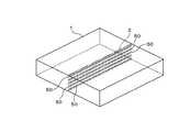
上記のようにして、X軸方向およびY軸方向と平行な全ての分割予定ライン2に沿ってレーザ光線が照射されてウェーハ内部に変質層が形成されるが、本実施形態では、1本の分割予定ライン2に対するレーザ光線照射動作を、複数回にわたって行い、かつ、この動作を繰り返す都度、レーザ光線の焦点位置を、ウェーハ1の、チャックテーブル11に近接する裏面近傍部分から表面側にわたって段階的に変化させて、図3に示すように、変質層50を複数層形成する(第1のレーザ光線照射工程)。さらにこの工程の後には、複数の変質層50の間にレーザ光線を照射する(第2のレーザ光線照射工程)。以下に、これら工程について詳述する。 As described above, the laser beam is irradiated along all the
[2−1]第1のレーザ光線照射工程
図4(a)に示すように、1本の分割予定ライン2の、ウェーハ1の内部における裏面1bに近接した高さ位置にレーザ光線Lの焦点位置を合わせ、その分割予定ライン2に沿って水平にレーザ光線Lを照射して、変質層50(第1の変質層50a)を形成する。変質層50aが形成されるに伴い、この変質層50aからは上方の表面側に延びる多数のクラックからなるクラック層51が形成される。ここでは、第1の変質層50aと、この第1の変質層50aから派生したクラック層51とを複合層(第1の複合層52A)52と称する。[2-1] First Laser Beam Irradiation Step As shown in FIG. 4A, the focal point of the laser beam L at a height position in the vicinity of the
次いで図4(b)に示すように、第1の複合層52Aの上方(ウェーハの表面1a側)に、間隔を空けて段階的にレーザ光線Lを照射して、複数の複合層52を形成する。この場合、複合層52を5層(第1〜第5の複合層52A,52B,52C,52D,52E)形成しており、これら複合層52(52A〜52E)は、第1〜第5の変質層50a,50b,50c,50d,50eにクラック層51が派生してなるものである。また、各複合層52の間隔は均等であって、その間隔は必ず確保され、そのためのレーザ光線の焦点位置の厚さ方向の間隔は、例えば20μm程度とされる。第1のレーザ光線照射工程において複合層52の直上に照射するレーザ光線の焦点位置は、直下の複合層52のクラック層51よりも上方に設定され、したがって複合層52間にはクラック層51が存在しない非クラック層53が設けられる。なお、複合層52はウェーハ1の厚さ全域にわたっては形成せず、最も表面側の複合層52と表面1aとの間には所定の間隔を空けておく。これは、表面1aに形成された半導体チップ3をレーザ光線で損傷させないためである。 Next, as shown in FIG. 4B, a plurality of
[2−2]第2のレーザ光線照射工程
図4(c)に示すように、ウェーハ1の裏面1bに最も近接した複合層52Aと、その上の複合層52Bとの間の非クラック層53に、レーザ光線Lの焦点位置を合わせて照射する。これによって、変質層50aの形成時に形成されたクラック層51は上方に延伸し、延伸クラック層54が上方の変質層50bに到達する。このような非クラック層53へのレーザ光線Lの照射を、図4(d)に示すように複合層52の間の非クラック層53に対して行う。同図の場合は、複合層52C,52Dの間の非クラック層53にはあえてレーザ光線は照射していないが、全ての複合層52の間の非クラック層53にレーザ光線を照射してもよい。[2-2] Second Laser Beam Irradiation Step As shown in FIG. 4C, the
このようにして1本の分割予定ライン2に複数の複合層52が形成され、かつ、これら複合層52の間の非クラック層53にレーザ光線Lが適宜照射されて、クラック層51が、隣接する変質層50に到達することにより、この後のウェーハ割断作業を容易、かつ確実に行うことができる。 In this way, a plurality of
例えば、直径:150mm、厚さ:400μm程度で、半導体チップ3のサイズが1.5mm程度のウェーハに対して、上記と同様に第1および第2のレーザ光線照射工程を行って5層の複合層52を形成し、かつ3層の延伸クラック層54を形成することにより、ウェーハを割断しやすくなる。この時のレーザ光線の照射条件は、レーザ光線の波長が1342nmのパルスレーザで、繰り返し周波数は150kHz、レーザ光線の集光レンズのNA(開口数)は0.8、チャックテーブル11の移動速度(XYテーブル13による加工送り速度)は300mm/secである。 For example, for a wafer having a diameter of about 150 mm and a thickness of about 400 μm and a
非クラック層53へのレーザ光線照射は1回でもよいが、XYテーブル13の往復動作で複数回にわたり重ねて行ってもよい。また、第1のレーザ光線照射工程での変質層50の形成のためのレーザ光線の波長と、第2のレーザ光線照射工程で非クラック層53に照射するレーザ光線の波長は同一であってよいが、異なる波長であってもよい。特に変質層50を形成するためのレーザ光線はパルスレーザであることが好ましく、一方、非クラック層53に照射するレーザ光線はパルスレーザの他、CW(Continuous Wave)レーザであってもよい。さらに、非クラック層53に照射するレーザ光線の集光レンズのNA(開口数)は、変質層50を形成するためのレーザ光線のものと同じか、もしくは小さい方が好ましい。 The
以上のようにして、X軸方向およびY軸方向に延びる全ての分割予定ライン2に対して複数層の複合層(変質層50+クラック層51)52を形成し、次に、複合層52間の全ての非クラック層53、あるいは適宜に選択した非クラック層53にレーザ光線Lを照射して延伸クラック層54を形成したら、ウェーハ1をチャックテーブル11から取り外し、次のウェーハ割断工程に移る。 As described above, a plurality of composite layers (modified
ウェーハ1の割断は、図5に示すように、周囲にダイシングフレーム61が貼り付けられたダイシングテープ62にウェーハ1の裏面側を貼着する。図中破線は、複合層(変質層50+クラック層51)52および延伸クラック層54が内部に形成されている分割予定ライン2を示している。ウェーハ1は、ダイシングテープ62およびダイシングフレーム61を介して、ブレーキング装置等の外力付与装置にセットされ、ダイシングテープ62にテンションを付与するなどの外力を付与されることにより、分割予定ライン2が割断され、各半導体チップ3に個片化される。 As shown in FIG. 5, the
[3]一実施形態の作用効果
上記一実施形態によれば、第1のレーザ光線照射工程によってウェーハ内部に形成された複数の複合層(変質層50+クラック層51)52の間には、クラック層が存在していない非クラック層53となっているが、この部分はクラック層51から延びる結晶欠陥などの影響によりレーザ光線を照射しても多光子吸収はなされず、変質層は形成されにくい。しかし、レーザ光線の照射によってすでに存在する変質層50から延びるクラック層51を延伸させる作用が見込まれる。第2のレーザ光線照射工程ではこの非クラック層53にレーザ光線を照射することにより、クラック層51を、隣接する変質層50に延伸させている。これによって第1のレーザ光線照射工程で形成されたクラック層51が、隣接する変質層50に到達し、このため、ウェーハ1の割断を、容易、かつ円滑に行うことができ、割断不良を招くことがないといった効果が奏される。[3] Advantageous Effects of One Embodiment According to the one embodiment, cracks are not formed between the plurality of composite layers (modified
また、第2のレーザ光線照射工程を行うことによって、第1のレーザ光線照射工程によって形成する変質層50の数を低減することができ、双方の工程によるレーザ光線照射の総回数も、従来の割断可能なレーザ光線照射回数より低減させることができる。このため、加工効率の低下も抑えられる。さらに、複合層52の間の全ての非クラック層53にレーザ光線を照射する必要はなく、適宜に選択した非クラック層53に照射しても割断は可能であり、このように第2のレーザ光線照射工程で全ての非クラック層53にレーザ光線を照射しない場合には、加工効率をより向上させることができる。 Further, by performing the second laser beam irradiation step, the number of altered
次に、本発明の実施例を説明して本発明の効果を実証する。なお、以下の実施例および比較例で作成したウェーハ試料は、それぞれ10枚ずつである。
[実施例1]
直径が150mmで厚さが400μmの素材段階のシリコンウェーハを試料とした。このウェーハは、格子状の分割予定ラインによって形成したチップ領域に電子回路を設けるといったデバイスパターンを表面に形成していない、いわゆる「ミラーウェーハ」である。このウェーハを、図2に示したものと同様のレーザ加工装置のチャックテーブルに表面側を上にしてセットした。そしてこのウェーハに、1.5mm間隔の仮想の分割予定ラインを設定し、全ての仮想分割予定ラインに、5層の複合層(変質層+クラック層)を、裏面に近接する位置から20μmの間隔をおいて段階的に形成し、次いで、複合層の間の4つの非クラック層のうちの3つに対してレーザ光線を照射し、延伸クラック層を形成した。すなわち、1本の分割予定ラインに対して、レーザ光線照射動作を8回行った。なお、レーザ光線はパルスレーザであり、照射の条件は以下の通りとした。Next, examples of the present invention will be described to demonstrate the effects of the present invention. The number of wafer samples prepared in the following examples and comparative examples is 10 each.
[Example 1]
A sample silicon wafer having a diameter of 150 mm and a thickness of 400 μm was used as a sample. This wafer is a so-called “mirror wafer” in which a device pattern is not formed on the surface such that an electronic circuit is provided in a chip region formed by a grid-like division line. This wafer was set on the chuck table of a laser processing apparatus similar to that shown in FIG. Then, virtual splitting lines with an interval of 1.5 mm are set on this wafer, and five composite layers (modified layers + crack layers) are placed on all the virtual splitting lines at a distance of 20 μm from the position close to the back surface. Then, three of the four non-crack layers between the composite layers were irradiated with a laser beam to form a stretched crack layer. That is, the laser beam irradiation operation was performed 8 times for one division planned line. The laser beam was a pulse laser, and the irradiation conditions were as follows.
・光源…LD励起QスイッチNd:YVO4レーザ
・波長…1342nm
・繰り返し周波数 …150kHz
・出力…出力1.2W(最も表面側の複合層を形成する際は0.6W)
・レーザ光線の集光レンズのNA(開口数)…0.8
・チャックテーブルの移動速度(加工送り速度)…300mm/sec
・パルス幅:105ns
・集光スポット径:φ1.5μmLight source: LD excitation Q switch Nd: YVO4 laser Wavelength: 1342 nm
・ Repetition frequency: 150 kHz
-Output: Output 1.2W (0.6W when forming the most surface side composite layer)
・ NA (numerical aperture) of condensing lens of laser beam ... 0.8
・ Movement speed of chuck table (processing feed speed) ... 300mm / sec
・ Pulse width: 105ns
・ Condensing spot diameter: φ1.5μm
[実施例2]
実施例1と同様のミラーウェーハの表面に、1.5mmの間隔で格子状の分割予定ラインを実際に形成し、さらに分割予定ラインで区画されたチップ領域に適宜な電子回路を形成して、デバイスパターンが形成された「パターンウェーハ」を試料として得た。このウェーハに対して、実施例1と全く同様にしてレーザ光線を照射し、全ての分割予定ラインの内部に、5層の複合層(変質層+クラック層)+3層の延伸非クラック層を形成した。[Example 2]
On the surface of the mirror wafer similar to that in Example 1, a grid-like division planned line is actually formed at an interval of 1.5 mm, and an appropriate electronic circuit is formed in a chip area partitioned by the division planned line, A “pattern wafer” on which a device pattern was formed was obtained as a sample. This wafer was irradiated with a laser beam in exactly the same manner as in Example 1 to form 5 composite layers (modified layer + crack layer) + 3 stretched non-crack layers inside all the division lines. did.
[比較例1]
実施例1と同様のミラーウェーハに対して、複合層を形成するレーザ光線の出力を0.8W(最も表面側の複合層を形成する際は0.5W)、形成する複合層を8層、複合層の間にはレーザ光線を照射しないという条件とし、この他は実施例1と同様の条件で、分割予定ラインに8層の複合層のみを形成した。[Comparative Example 1]
For the same mirror wafer as in Example 1, the output of the laser beam for forming the composite layer is 0.8 W (0.5 W when forming the composite layer on the most surface side), and 8 composite layers are formed. Only the composite layer of 8 layers was formed in the division | segmentation schedule line on the conditions which do not irradiate a laser beam between composite layers on the conditions similar to Example 1 except this.
[比較例2]
実施例2と同様のパターンウェーハに対して、比較例1と全く同様の条件でレーザ光線を照射し、分割予定ラインに8層の複合層のみを形成した。[Comparative Example 2]
The same pattern wafer as in Example 2 was irradiated with a laser beam under exactly the same conditions as in Comparative Example 1, and only 8 composite layers were formed on the planned division lines.
[比較例3]
実施例1と同様のミラーウェーハに対して、複合層を形成するレーザ光線の出力を1.2W(最も表面側の複合層を形成する際は0.6W)、形成する複合層を5層、複合層の間にはレーザ光線を照射しないという条件とし、この他は実施例1と同様の条件で、分割予定ラインに5層の複合層のみを形成した。[Comparative Example 3]
For the same mirror wafer as in Example 1, the output of the laser beam for forming the composite layer is 1.2 W (0.6 W when forming the composite layer on the most surface side), and 5 composite layers are formed. Only the composite layer of 5 layers was formed in the division | segmentation schedule line on the conditions which do not irradiate a laser beam between composite layers on the conditions similar to Example 1 except this.
[比較例4]
実施例2と同様のパターンウェーハに対して、比較例3と全く同様の条件でレーザ光線を照射し、分割予定ラインに5層の複合層のみを形成した。[Comparative Example 4]
The same pattern wafer as in Example 2 was irradiated with a laser beam under exactly the same conditions as in Comparative Example 3, and only five composite layers were formed on the planned division lines.
[割断試験]
実施例1,2および比較例1〜4の各ウェーハ10枚ずつを、図5に示すようにしてダイシングテープに貼着し、ブレーキング装置にセットして外力を付与してウェーハの割断を試みた。割断状況の結果は以下の通りであった。なお、割断率とは、1枚のウェーハに形成された半導体チップが全て分割して個片化された状況を100%としている。また、割断面を観察した結果を付記した。[Cleaving test]
Ten wafers of each of Examples 1 and 2 and Comparative Examples 1 to 4 are attached to a dicing tape as shown in FIG. 5, set on a braking device and applied with external force to try to cleave the wafer. It was. The result of the cleaving situation was as follows. The cleaving rate is defined as 100% when all the semiconductor chips formed on one wafer are divided and separated into individual pieces. Moreover, the result of observing the fractured surface was added.
・割断率
実施例1(ミラーウェーハ) … 割断率:100%
実施例2(パターンウェーハ) … 割断率:100%
比較例1(ミラーウェーハ) … 割断率: 90%
比較例2(パターンウェーハ) ※実施せず
比較例3(ミラーウェーハ) … 割断率:100%
比較例4(パターンウェーハ) … 10枚中2,3枚に2%程度の割れ残り発生-Cleaving rate Example 1 (mirror wafer) ... Cleaving rate: 100%
Example 2 (pattern wafer) ... Cleaving rate: 100%
Comparative Example 1 (mirror wafer) ... Cleaving rate: 90%
Comparative example 2 (pattern wafer) * Not implemented Comparative example 3 (mirror wafer) ... Cleaving rate: 100%
Comparative Example 4 (pattern wafer) ... 2% of 10 out of 2 cracks remaining on 2 sheets
・割断面の状態
変質層が5層の実施例1,2および比較例3,4の割断面はほぼ同様であり、変質層と結晶層(非クラック層)の交互の縞模様が明確に観察された。これは、ウェーハ厚さに対する変質層の数が比較的少なく、変質層の間隔が大きかったためとみられる。一方、変質層が8層の比較例1,2では、変質層の数が多いことから隣接する変質層どうしがかなり近接し、連続しているように見えた。-State of fractured surface The fractured surfaces of Examples 1 and 2 and Comparative Examples 3 and 4 with 5 altered layers are almost the same, and the alternating stripe pattern of the altered layer and the crystalline layer (non-cracked layer) is clearly observed. It was done. This is probably because the number of deteriorated layers relative to the wafer thickness is relatively small and the interval between the deteriorated layers is large. On the other hand, in Comparative Examples 1 and 2 having 8 deteriorated layers, since the number of deteriorated layers was large, adjacent deteriorated layers appeared to be quite close and continuous.
上記の結果によれば、本発明に基づく実施例1,2は割断率が100%と良好な結果を示した。一方、実施例1,2において行った変質層間へのレーザ光線照射を省略した比較例3,4では、比較的割断されやすいミラーウェーハ(比較例3)では割断率が100%であったものの、割断されにくいパターンウェーハ(比較例4)は100%を得られなかった。これにより、変質層間の非クラック層にレーザ光線を照射してクラック層を変質層に到達させることによる本発明の効果が実証された。また、比較例1,2のうち、ミラーウェーハは割断率が90%であり、変質層が比較的密に形成されることによる割断率の低下が認められた。なお、比較例2のパターンウェーハはミラーウェーハよりも割断されにくいものであることから、割断率が90%を超えることは望めず、したがって割断は実施しなかった。 According to said result, Example 1, 2 based on this invention showed the favorable result with a cleaving rate of 100%. On the other hand, in Comparative Examples 3 and 4 in which the laser beam irradiation to the altered layer performed in Examples 1 and 2 was omitted, although the cleaving rate was 100% in the relatively easily cleaved mirror wafer (Comparative Example 3), The pattern wafer (Comparative Example 4) that is difficult to cleave could not obtain 100%. Thereby, the effect of the present invention by irradiating the non-cracked layer between the altered layers with a laser beam to reach the altered layer was demonstrated. In Comparative Examples 1 and 2, the mirror wafer had a cleaving rate of 90%, and a reduction in the cleaving rate was observed due to the formation of the altered layer relatively densely. In addition, since the pattern wafer of Comparative Example 2 is more difficult to cleave than a mirror wafer, the cleaving rate cannot be expected to exceed 90%, and therefore cleaving was not performed.
1…半導体ウェーハ
1a…ウェーハの表面(一面)
1b…ウェーハの裏面(他面)
2…分割予定ライン
3…半導体チップ
10…レーザ加工装置
11…チャックテーブル(保持台)
50…変質層
51…クラック層
54…延伸クラック層
52…複合層
53…非クラック層
L…レーザ光線DESCRIPTION OF
1b ... Back side of wafer (other side)
2 ...
50 ...
Claims (2)
Translated fromJapanese保持台に、ウェーハの他面を合わせ、かつ、一面を露出させて保持するウェーハ保持工程と、
前記レーザ光線照射動作を、前記保持台に保持したウェーハの前記他面側から前記一面側にわたって複数回行うことにより、前記変質層と、該変質層から一面方向に延びるクラック層とからなる複数の複合層を、入射方向に間隔を空けて段階的に形成する第1のレーザ光線照射工程と、
第1のレーザ光線照射工程で形成された複数の前記複合層の間に、レーザ光線の焦点位置を合わせてレーザ光線を照射し、これによって前記クラック層を前記一面方向に延伸させて該方向に隣接する前記変質層に到達させる第2のレーザ光線照射工程と
を備えることを特徴とするウェーハのレーザ加工方法。When performing laser beam irradiation operation for irradiating the inside of the wafer from one side of the wafer along the scheduled division line formed on the wafer a plurality of times, the focal position of the laser beam is changed each time the operation is performed. A method of laser processing a wafer, wherein a plurality of altered layers along a predetermined division line are formed in the wafer in a stepwise manner in the incident direction, thereby forming a plurality of altered layers in the thickness direction of the wafer,
A wafer holding step for aligning the other surface of the wafer with the holding table and exposing and holding one surface,
By performing the laser beam irradiation operation a plurality of times from the other surface side to the one surface side of the wafer held on the holding table, a plurality of the altered layer and a plurality of crack layers extending in the one surface direction from the altered layer. A first laser beam irradiation step of forming the composite layer stepwise with an interval in the incident direction;
A laser beam is irradiated between the plurality of composite layers formed in the first laser beam irradiation step so that the focal position of the laser beam is adjusted, thereby extending the crack layer in the one surface direction in this direction. And a second laser beam irradiation step for arriving at the deteriorated layer adjacent thereto.
Priority Applications (2)
| Application Number | Priority Date | Filing Date | Title |
|---|---|---|---|
| JP2007168933AJP5162163B2 (en) | 2007-06-27 | 2007-06-27 | Wafer laser processing method |
| US12/138,623US7642174B2 (en) | 2007-06-27 | 2008-06-13 | Laser beam machining method for wafer |
Applications Claiming Priority (1)
| Application Number | Priority Date | Filing Date | Title |
|---|---|---|---|
| JP2007168933AJP5162163B2 (en) | 2007-06-27 | 2007-06-27 | Wafer laser processing method |
Publications (2)
| Publication Number | Publication Date |
|---|---|
| JP2009010105Atrue JP2009010105A (en) | 2009-01-15 |
| JP5162163B2 JP5162163B2 (en) | 2013-03-13 |
Family
ID=40161090
Family Applications (1)
| Application Number | Title | Priority Date | Filing Date |
|---|---|---|---|
| JP2007168933AActiveJP5162163B2 (en) | 2007-06-27 | 2007-06-27 | Wafer laser processing method |
Country Status (2)
| Country | Link |
|---|---|
| US (1) | US7642174B2 (en) |
| JP (1) | JP5162163B2 (en) |
Cited By (19)
| Publication number | Priority date | Publication date | Assignee | Title |
|---|---|---|---|---|
| WO2010090111A1 (en)* | 2009-02-09 | 2010-08-12 | 浜松ホトニクス株式会社 | Workpiece cutting method |
| WO2010122866A1 (en)* | 2009-04-20 | 2010-10-28 | 浜松ホトニクス株式会社 | Laser machining method |
| JP2010247189A (en)* | 2009-04-16 | 2010-11-04 | Shin Etsu Polymer Co Ltd | Method of manufacturing semiconductor wafer and apparatus therefor |
| WO2011013449A1 (en)* | 2009-07-29 | 2011-02-03 | 西進商事株式会社 | Laser scribe processing method |
| WO2011093113A1 (en)* | 2010-01-27 | 2011-08-04 | 浜松ホトニクス株式会社 | Laser processing method |
| JP2012084682A (en)* | 2010-10-12 | 2012-04-26 | Disco Abrasive Syst Ltd | Method for dividing optical device unit |
| JP2012091233A (en)* | 2009-08-03 | 2012-05-17 | Hamamatsu Photonics Kk | Laser beam machining method |
| JP2013048244A (en)* | 2011-07-27 | 2013-03-07 | Toshiba Mach Co Ltd | Laser dicing method |
| JP2013175499A (en)* | 2012-02-23 | 2013-09-05 | Disco Abrasive Syst Ltd | Method of dividing wafer |
| US8755107B2 (en) | 2010-01-27 | 2014-06-17 | Hamamatsu Photonics K.K. | Laser processing system |
| US8871540B2 (en) | 2011-07-27 | 2014-10-28 | Toshiba Kikai Kabushiki Kaisha | Laser dicing method |
| US8895345B2 (en) | 2010-06-24 | 2014-11-25 | Toshiba Kikai Kabushiki Kaisha | Dicing methods |
| JP2015030040A (en)* | 2013-08-02 | 2015-02-16 | ロフィン−ジナール テクノロジーズ インコーポレイテッド | System for performing laser filamentation within transparent material |
| US9050683B2 (en) | 2012-06-29 | 2015-06-09 | Toshiba Kikai Kabushiki Kaisha | Laser dicing method |
| JP2016146446A (en)* | 2015-02-09 | 2016-08-12 | 株式会社ディスコ | Wafer generation method |
| JP2018207009A (en)* | 2017-06-07 | 2018-12-27 | 株式会社ディスコ | Workpiece processing method |
| KR20210108310A (en) | 2020-02-25 | 2021-09-02 | 가부시기가이샤 디스코 | Method of manufacturing chip |
| JP2023026125A (en)* | 2021-08-12 | 2023-02-24 | 株式会社ディスコ | Processing method of work-piece |
| JP2023032215A (en)* | 2021-08-26 | 2023-03-09 | 株式会社ディスコ | Processing method |
Families Citing this family (14)
| Publication number | Priority date | Publication date | Assignee | Title |
|---|---|---|---|---|
| JP4634089B2 (en)* | 2004-07-30 | 2011-02-16 | 浜松ホトニクス株式会社 | Laser processing method |
| KR100674440B1 (en)* | 2005-08-12 | 2007-01-25 | 주식회사 파이컴 | Probe card manufacturing method and apparatus |
| US20110300692A1 (en)* | 2008-10-29 | 2011-12-08 | Oerlikon Solar Ag, Trubbach | Method for dividing a semiconductor film formed on a substrate into plural regions by multiple laser beam irradiation |
| JP5379604B2 (en) | 2009-08-21 | 2013-12-25 | 浜松ホトニクス株式会社 | Laser processing method and chip |
| JP5620669B2 (en)* | 2009-10-26 | 2014-11-05 | 東芝機械株式会社 | Laser dicing method and laser dicing apparatus |
| JP5452247B2 (en)* | 2010-01-21 | 2014-03-26 | 東芝機械株式会社 | Laser dicing equipment |
| JP5507294B2 (en)* | 2010-03-05 | 2014-05-28 | 東芝機械株式会社 | Grinding machine with distance measuring function |
| EP2657958B1 (en)* | 2010-11-10 | 2016-02-10 | Toyota Jidosha Kabushiki Kaisha | Method of manufacturing semiconductor device |
| US9636783B2 (en) | 2014-04-30 | 2017-05-02 | International Business Machines Corporation | Method and apparatus for laser dicing of wafers |
| JP6669594B2 (en)* | 2016-06-02 | 2020-03-18 | 株式会社ディスコ | Wafer generation method |
| JP6935224B2 (en)* | 2017-04-25 | 2021-09-15 | 株式会社ディスコ | Wafer generation method |
| JP7033485B2 (en)* | 2018-04-17 | 2022-03-10 | 株式会社ディスコ | Cutting blade shaping method |
| CN108827689A (en)* | 2018-09-06 | 2018-11-16 | 广东工业大学 | A kind of cell micro-dissection system |
| US11664276B2 (en)* | 2018-11-30 | 2023-05-30 | Texas Instruments Incorporated | Front side laser-based wafer dicing |
Citations (4)
| Publication number | Priority date | Publication date | Assignee | Title |
|---|---|---|---|---|
| JP2006108459A (en)* | 2004-10-07 | 2006-04-20 | Disco Abrasive Syst Ltd | Laser processing method and laser processing apparatus for silicon wafer |
| JP2006315017A (en)* | 2005-05-11 | 2006-11-24 | Canon Inc | Laser cutting method and member to be cut |
| JP2006332556A (en)* | 2005-05-30 | 2006-12-07 | Disco Abrasive Syst Ltd | Wafer division method |
| JP2007157887A (en)* | 2005-12-02 | 2007-06-21 | Disco Abrasive Syst Ltd | Wafer division method |
Family Cites Families (8)
| Publication number | Priority date | Publication date | Assignee | Title |
|---|---|---|---|---|
| JP4659300B2 (en)* | 2000-09-13 | 2011-03-30 | 浜松ホトニクス株式会社 | Laser processing method and semiconductor chip manufacturing method |
| JP3626442B2 (en) | 2000-09-13 | 2005-03-09 | 浜松ホトニクス株式会社 | Laser processing method |
| KR100701013B1 (en)* | 2001-05-21 | 2007-03-29 | 삼성전자주식회사 | Method and apparatus for cutting non-metallic substrate using laser beam |
| JP2005268752A (en)* | 2004-02-19 | 2005-09-29 | Canon Inc | Laser cleaving method, member to be cleaved, and semiconductor element chip |
| US7550367B2 (en)* | 2004-08-17 | 2009-06-23 | Denso Corporation | Method for separating semiconductor substrate |
| JP4942313B2 (en)* | 2005-07-07 | 2012-05-30 | 株式会社ディスコ | Wafer laser processing method |
| JP4769560B2 (en)* | 2005-12-06 | 2011-09-07 | 株式会社ディスコ | Wafer division method |
| JP2007235008A (en)* | 2006-03-03 | 2007-09-13 | Denso Corp | Dividing method for wafer, and chip |
- 2007
- 2007-06-27JPJP2007168933Apatent/JP5162163B2/enactiveActive
- 2008
- 2008-06-13USUS12/138,623patent/US7642174B2/enactiveActive
Patent Citations (4)
| Publication number | Priority date | Publication date | Assignee | Title |
|---|---|---|---|---|
| JP2006108459A (en)* | 2004-10-07 | 2006-04-20 | Disco Abrasive Syst Ltd | Laser processing method and laser processing apparatus for silicon wafer |
| JP2006315017A (en)* | 2005-05-11 | 2006-11-24 | Canon Inc | Laser cutting method and member to be cut |
| JP2006332556A (en)* | 2005-05-30 | 2006-12-07 | Disco Abrasive Syst Ltd | Wafer division method |
| JP2007157887A (en)* | 2005-12-02 | 2007-06-21 | Disco Abrasive Syst Ltd | Wafer division method |
Cited By (36)
| Publication number | Priority date | Publication date | Assignee | Title |
|---|---|---|---|---|
| WO2010090111A1 (en)* | 2009-02-09 | 2010-08-12 | 浜松ホトニクス株式会社 | Workpiece cutting method |
| KR101757937B1 (en)* | 2009-02-09 | 2017-07-13 | 하마마츠 포토닉스 가부시키가이샤 | Workpiece cutting method |
| CN102307699B (en)* | 2009-02-09 | 2015-07-15 | 浜松光子学株式会社 | Cutting method of object to be processed |
| CN102307699A (en)* | 2009-02-09 | 2012-01-04 | 浜松光子学株式会社 | Workpiece cutting method |
| US8728914B2 (en) | 2009-02-09 | 2014-05-20 | Hamamatsu Photonics K.K. | Workpiece cutting method |
| JP5632751B2 (en)* | 2009-02-09 | 2014-11-26 | 浜松ホトニクス株式会社 | Processing object cutting method |
| US8865568B2 (en) | 2009-02-09 | 2014-10-21 | Hamamatsu Photonics K.K | Workpiece cutting method |
| JP2010247189A (en)* | 2009-04-16 | 2010-11-04 | Shin Etsu Polymer Co Ltd | Method of manufacturing semiconductor wafer and apparatus therefor |
| WO2010122866A1 (en)* | 2009-04-20 | 2010-10-28 | 浜松ホトニクス株式会社 | Laser machining method |
| CN102405124A (en)* | 2009-04-20 | 2012-04-04 | 浜松光子学株式会社 | Laser machining method |
| US9076855B2 (en) | 2009-04-20 | 2015-07-07 | Hamamatsu Photonics K.K. | Laser machining method |
| WO2011013449A1 (en)* | 2009-07-29 | 2011-02-03 | 西進商事株式会社 | Laser scribe processing method |
| US8779327B2 (en) | 2009-07-29 | 2014-07-15 | Seishin Trading Co., Ltd. | Laser scribe processing method |
| JP2012091233A (en)* | 2009-08-03 | 2012-05-17 | Hamamatsu Photonics Kk | Laser beam machining method |
| JP2012115906A (en)* | 2009-08-03 | 2012-06-21 | Hamamatsu Photonics Kk | Laser beam machining device |
| US8755107B2 (en) | 2010-01-27 | 2014-06-17 | Hamamatsu Photonics K.K. | Laser processing system |
| WO2011093113A1 (en)* | 2010-01-27 | 2011-08-04 | 浜松ホトニクス株式会社 | Laser processing method |
| US8828891B2 (en) | 2010-01-27 | 2014-09-09 | Hamamatsu Photonics K.K. | Laser processing method |
| CN102725096A (en)* | 2010-01-27 | 2012-10-10 | 浜松光子学株式会社 | Laser processing method |
| KR101757952B1 (en) | 2010-01-27 | 2017-07-13 | 하마마츠 포토닉스 가부시키가이샤 | Laser processing method |
| TWI501831B (en)* | 2010-01-27 | 2015-10-01 | Hamamatsu Photonics Kk | Laser processing method |
| JP2011152561A (en)* | 2010-01-27 | 2011-08-11 | Hamamatsu Photonics Kk | Laser machining method |
| US8895345B2 (en) | 2010-06-24 | 2014-11-25 | Toshiba Kikai Kabushiki Kaisha | Dicing methods |
| JP2012084682A (en)* | 2010-10-12 | 2012-04-26 | Disco Abrasive Syst Ltd | Method for dividing optical device unit |
| US8871540B2 (en) | 2011-07-27 | 2014-10-28 | Toshiba Kikai Kabushiki Kaisha | Laser dicing method |
| JP2013048244A (en)* | 2011-07-27 | 2013-03-07 | Toshiba Mach Co Ltd | Laser dicing method |
| JP2013175499A (en)* | 2012-02-23 | 2013-09-05 | Disco Abrasive Syst Ltd | Method of dividing wafer |
| US9050683B2 (en) | 2012-06-29 | 2015-06-09 | Toshiba Kikai Kabushiki Kaisha | Laser dicing method |
| JP2015037808A (en)* | 2013-08-02 | 2015-02-26 | ロフィン−ジナール テクノロジーズ インコーポレイテッド | Method and apparatus for performing laser filamentation inside a transparent material |
| JP2015030040A (en)* | 2013-08-02 | 2015-02-16 | ロフィン−ジナール テクノロジーズ インコーポレイテッド | System for performing laser filamentation within transparent material |
| JP2016146446A (en)* | 2015-02-09 | 2016-08-12 | 株式会社ディスコ | Wafer generation method |
| JP2018207009A (en)* | 2017-06-07 | 2018-12-27 | 株式会社ディスコ | Workpiece processing method |
| KR20210108310A (en) | 2020-02-25 | 2021-09-02 | 가부시기가이샤 디스코 | Method of manufacturing chip |
| JP2023026125A (en)* | 2021-08-12 | 2023-02-24 | 株式会社ディスコ | Processing method of work-piece |
| JP7693447B2 (en) | 2021-08-12 | 2025-06-17 | 株式会社ディスコ | Workpiece machining method |
| JP2023032215A (en)* | 2021-08-26 | 2023-03-09 | 株式会社ディスコ | Processing method |
Also Published As
| Publication number | Publication date |
|---|---|
| JP5162163B2 (en) | 2013-03-13 |
| US7642174B2 (en) | 2010-01-05 |
| US20090004828A1 (en) | 2009-01-01 |
Similar Documents
| Publication | Publication Date | Title |
|---|---|---|
| JP5162163B2 (en) | Wafer laser processing method | |
| KR101979397B1 (en) | Method of dividing substrate with pattern | |
| JP2010003817A (en) | Laser dicing method, and laser dicing device | |
| JP5090897B2 (en) | Wafer dividing method | |
| JP2006150385A (en) | Laser cleaving method | |
| KR20090123777A (en) | Wafer Segmentation Method | |
| JP2007173475A (en) | Wafer division method | |
| JP2007317935A (en) | Semiconductor substrate, substrate cleaving method, and element chip manufacturing method | |
| TWI697946B (en) | Wafer processing method | |
| KR20090124928A (en) | Wafer Segmentation Method | |
| JP2006108273A (en) | Wafer dividing method and dividing apparatus | |
| CN105935842A (en) | Method of manufacturing device chips | |
| CN107053499B (en) | wafer processing method | |
| KR20210108310A (en) | Method of manufacturing chip | |
| TWI704608B (en) | Wafer processing method | |
| JP5453123B2 (en) | Cutting method | |
| JP5598801B2 (en) | Laser dicing method, chip manufacturing method, and laser processing apparatus | |
| JP2011171382A (en) | Dividing method | |
| CN107030389B (en) | wafer processing method | |
| JP5116382B2 (en) | Laser processing method | |
| JP2014121718A (en) | Laser machining apparatus | |
| KR101012332B1 (en) | Semiconductor wafer cutting system | |
| JP6525840B2 (en) | Wafer processing method | |
| JP6525833B2 (en) | Wafer processing method | |
| JP2007194515A (en) | Wafer division method |
Legal Events
| Date | Code | Title | Description |
|---|---|---|---|
| A621 | Written request for application examination | Free format text:JAPANESE INTERMEDIATE CODE: A621 Effective date:20100511 | |
| A977 | Report on retrieval | Free format text:JAPANESE INTERMEDIATE CODE: A971007 Effective date:20120517 | |
| A131 | Notification of reasons for refusal | Free format text:JAPANESE INTERMEDIATE CODE: A131 Effective date:20120521 | |
| A521 | Request for written amendment filed | Free format text:JAPANESE INTERMEDIATE CODE: A523 Effective date:20120719 | |
| A131 | Notification of reasons for refusal | Free format text:JAPANESE INTERMEDIATE CODE: A131 Effective date:20120831 | |
| A521 | Request for written amendment filed | Free format text:JAPANESE INTERMEDIATE CODE: A523 Effective date:20121030 | |
| TRDD | Decision of grant or rejection written | ||
| A01 | Written decision to grant a patent or to grant a registration (utility model) | Free format text:JAPANESE INTERMEDIATE CODE: A01 Effective date:20121129 | |
| A61 | First payment of annual fees (during grant procedure) | Free format text:JAPANESE INTERMEDIATE CODE: A61 Effective date:20121217 | |
| R150 | Certificate of patent or registration of utility model | Ref document number:5162163 Country of ref document:JP Free format text:JAPANESE INTERMEDIATE CODE: R150 Free format text:JAPANESE INTERMEDIATE CODE: R150 | |
| FPAY | Renewal fee payment (event date is renewal date of database) | Free format text:PAYMENT UNTIL: 20151221 Year of fee payment:3 | |
| FPAY | Renewal fee payment (event date is renewal date of database) | Free format text:PAYMENT UNTIL: 20151221 Year of fee payment:3 | |
| R250 | Receipt of annual fees | Free format text:JAPANESE INTERMEDIATE CODE: R250 | |
| R250 | Receipt of annual fees | Free format text:JAPANESE INTERMEDIATE CODE: R250 | |
| R250 | Receipt of annual fees | Free format text:JAPANESE INTERMEDIATE CODE: R250 | |
| R250 | Receipt of annual fees | Free format text:JAPANESE INTERMEDIATE CODE: R250 | |
| R250 | Receipt of annual fees | Free format text:JAPANESE INTERMEDIATE CODE: R250 | |
| R250 | Receipt of annual fees | Free format text:JAPANESE INTERMEDIATE CODE: R250 | |
| R250 | Receipt of annual fees | Free format text:JAPANESE INTERMEDIATE CODE: R250 | |
| R250 | Receipt of annual fees | Free format text:JAPANESE INTERMEDIATE CODE: R250 | |
| R250 | Receipt of annual fees | Free format text:JAPANESE INTERMEDIATE CODE: R250 | |
| R250 | Receipt of annual fees | Free format text:JAPANESE INTERMEDIATE CODE: R250 |