JP2009009571A - Method and device for level 2 cache/nest address translation - Google Patents
Method and device for level 2 cache/nest address translationDownload PDFInfo
- Publication number
- JP2009009571A JP2009009571AJP2008165291AJP2008165291AJP2009009571AJP 2009009571 AJP2009009571 AJP 2009009571AJP 2008165291 AJP2008165291 AJP 2008165291AJP 2008165291 AJP2008165291 AJP 2008165291AJP 2009009571 AJP2009009571 AJP 2009009571A
- Authority
- JP
- Japan
- Prior art keywords
- cache
- level
- caches
- address
- processor
- Prior art date
- Legal status (The legal status is an assumption and is not a legal conclusion. Google has not performed a legal analysis and makes no representation as to the accuracy of the status listed.)
- Pending
Links
Images


Classifications
- G—PHYSICS
- G06—COMPUTING OR CALCULATING; COUNTING
- G06F—ELECTRIC DIGITAL DATA PROCESSING
- G06F12/00—Accessing, addressing or allocating within memory systems or architectures
- G06F12/02—Addressing or allocation; Relocation
- G06F12/08—Addressing or allocation; Relocation in hierarchically structured memory systems, e.g. virtual memory systems
- G06F12/10—Address translation
- G06F12/1027—Address translation using associative or pseudo-associative address translation means, e.g. translation look-aside buffer [TLB]
- G06F12/1045—Address translation using associative or pseudo-associative address translation means, e.g. translation look-aside buffer [TLB] associated with a data cache
- G06F12/1063—Address translation using associative or pseudo-associative address translation means, e.g. translation look-aside buffer [TLB] associated with a data cache the data cache being concurrently virtually addressed
- G—PHYSICS
- G06—COMPUTING OR CALCULATING; COUNTING
- G06F—ELECTRIC DIGITAL DATA PROCESSING
- G06F12/00—Accessing, addressing or allocating within memory systems or architectures
- G06F12/02—Addressing or allocation; Relocation
- G06F12/08—Addressing or allocation; Relocation in hierarchically structured memory systems, e.g. virtual memory systems
- G06F12/0802—Addressing of a memory level in which the access to the desired data or data block requires associative addressing means, e.g. caches
- G06F12/0806—Multiuser, multiprocessor or multiprocessing cache systems
- G06F12/0811—Multiuser, multiprocessor or multiprocessing cache systems with multilevel cache hierarchies
- Y—GENERAL TAGGING OF NEW TECHNOLOGICAL DEVELOPMENTS; GENERAL TAGGING OF CROSS-SECTIONAL TECHNOLOGIES SPANNING OVER SEVERAL SECTIONS OF THE IPC; TECHNICAL SUBJECTS COVERED BY FORMER USPC CROSS-REFERENCE ART COLLECTIONS [XRACs] AND DIGESTS
- Y02—TECHNOLOGIES OR APPLICATIONS FOR MITIGATION OR ADAPTATION AGAINST CLIMATE CHANGE
- Y02D—CLIMATE CHANGE MITIGATION TECHNOLOGIES IN INFORMATION AND COMMUNICATION TECHNOLOGIES [ICT], I.E. INFORMATION AND COMMUNICATION TECHNOLOGIES AIMING AT THE REDUCTION OF THEIR OWN ENERGY USE
- Y02D10/00—Energy efficient computing, e.g. low power processors, power management or thermal management
Landscapes
- Engineering & Computer Science (AREA)
- Theoretical Computer Science (AREA)
- Physics & Mathematics (AREA)
- General Engineering & Computer Science (AREA)
- General Physics & Mathematics (AREA)
- Memory System Of A Hierarchy Structure (AREA)
Abstract
Description
Translated fromJapanese本発明は、一般的には、プロセッサにおける命令の実行に関するものである。 The present invention generally relates to the execution of instructions in a processor.
現在のコンピュータ・システムは、一般に、コンピュータ・システムにおいて情報を処理するために使用し得るプロセッサを含む幾つもの集積回路(IC)を内蔵している。プロセッサによって処理されるデータは、プロセッサによって実行されるコンピュータ命令と、コンピュータ命令を使用してプロセッサにより操作されるデータとを含み得る。コンピュータ命令およびデータは、一般に、コンピュータ・システムにおけるメイン・メモリに格納される。 Current computer systems typically incorporate a number of integrated circuits (ICs) that include a processor that can be used to process information in the computer system. Data processed by the processor may include computer instructions executed by the processor and data manipulated by the processor using computer instructions. Computer instructions and data are typically stored in main memory in a computer system.
プロセッサは、一般に、一連の小さいステップで命令を実行することによって命令を処理する。場合によっては、プロセッサによって処理される命令の数を増加させるために(従って、プロセッサの速度を高めるために)、プロセッサがパイプライン化されることがある。パイプライン化はプロセッサ内に個別のステージを設けることを指し、その場合、各ステージが、命令を実行するために必要な1つまたは複数の小さいステップを遂行する。場合によっては、パイプラインは、(他の回路に加えて)、プロセッサ・コアと呼ばれるプロセッサの一部に設けられることもある。 A processor typically processes instructions by executing the instructions in a series of small steps. In some cases, the processor may be pipelined to increase the number of instructions processed by the processor (and thus to increase the speed of the processor). Pipelining refers to providing separate stages within a processor, where each stage performs one or more small steps necessary to execute an instruction. In some cases, the pipeline (in addition to other circuitry) may be provided in a portion of the processor called the processor core.
プロセッサは、データおよび命令に対する速いアクセス並びにプロセッサの良好な利用を提供するために、幾つものキャッシュを有することがある。キャッシュは、一般にメイン・メモリよりも小さく、一般にプロセッサと同じダイ(即ち、チップ)上に作成されたメモリである。現在のプロセッサは、一般に幾つものレベルのキャッシュを有する。プロセッサのコアに最も近接して設けられる最速のキャッシュはレベル1キャッシュ(L1キャッシュ)と呼ばれる。プロセッサは、一般に、L1キャッシュのほかに、レベル2キャッシュ(L2キャッシュ)と呼ばれる二次的な大型キャッシュを有する。場合によっては、プロセッサは、他の更なるキャッシュ・レベル(例えば、L3キャッシュおよびL4キャッシュ)を有することもある。 A processor may have several caches to provide fast access to data and instructions and good utilization of the processor. A cache is memory that is typically smaller than main memory and is typically created on the same die (ie, chip) as the processor. Current processors typically have several levels of cache. The fastest cache provided closest to the core of the processor is called a
現在のプロセッサは、大きな実アドレスのセットをアクセスするために、ソフトウェア・プログラムが1セットの有効アドレスを使用することを可能にする、アドレス変換を提供する。キャッシュへのアクセス中に、ロードまたはストア命令によって提供される有効アドレスが、実アドレスに変換され、L1キャッシュにアクセスするために使用され得る。従って、プロセッサは、L1キャッシュがロード命令またはストア命令によってアクセスされる前に、アドレス変換を行うように構成された回路を含むことがある。しかし、アドレス変換のために、L1キャッシュに対するアクセス・タイムが増加することがある。更に、各コアがアドレス変換を行うような複数のコアをプロセッサが含む場合、アドレス変換回路を設けるオーバヘッドおよび複数のプログラムを実行しながらアドレス変換を行うオーバヘッドは望ましくないものになることがある。 Current processors provide address translation that allows a software program to use a set of effective addresses to access a large set of real addresses. During access to the cache, the effective address provided by the load or store instruction can be converted to a real address and used to access the L1 cache. Thus, the processor may include circuitry configured to perform address translation before the L1 cache is accessed by a load or store instruction. However, access time for the L1 cache may increase due to address translation. Furthermore, when a processor includes a plurality of cores in which each core performs address conversion, the overhead of providing an address conversion circuit and the overhead of performing address conversion while executing a plurality of programs may be undesirable.
従って、必要なことは、プロセッサ・キャッシュをアクセスするための方法および装置の改良である。 Therefore, what is needed is an improved method and apparatus for accessing the processor cache.
本発明の目的は、一般的には、プロセッサ・コアをアクセスするための方法を提供することである。 An object of the present invention is generally to provide a method for accessing a processor core.
本発明の方法の一実施例は、要求されたデータの要求された有効アドレスを使用して、プロセッサの1つまたは複数のレベル1キャッシュにおいてその要求されたデータをアクセスする。プロセッサの1つまたは複数のレベル1キャッシュがその要求された有効アドレスに対応する要求されたデータを含んでいない場合、その要求された有効アドレスは実アドレスに変換される。ルックアサイド・バッファが、プロセッサの1つまたは複数のレベル1キャッシュの各々における各キャッシュ・ラインに対して1つの対応するエントリを含む。対応するエントリは、有効アドレスからキャッシュ・ラインに対する実アドレスへの変換を表す。変換された実アドレスはレベル2キャッシュをアクセスするために使用される。 One embodiment of the method of the present invention uses the requested effective address of the requested data to access the requested data in one or
本発明の一実施例は、1つまたは複数のレベル1キャッシュ、1つのレベル2キャッシュ、およびルックアサイド・バッファを含むプロセッサも提供する。プロセッサは、更に、要求されたデータの要求された有効アドレスを使用して、プロセッサの1つまたは複数のレベル1キャッシュにおける要求されたデータをアクセスするように構成された回路を含む。プロセッサの1つまたは複数のレベル1キャッシュがその要求された有効アドレスに対応する要求されたデータを含んでいない場合、要求された有効アドレスは実アドレスに変換される。ルックアサイド・バッファは、プロセッサの1つまたは複数のレベル1キャッシュの各々における各キャッシュ・ラインに対する対応するエントリを含んでいる。その対応するエントリは、有効アドレスからキャッシュ・ラインに対する実アドレスへの変換を表す。回路は、レベル2のキャッシュをアクセスするためにその変換された実アドレスを使用するようにも構成される。 One embodiment of the present invention also provides a processor that includes one or
本発明の一実施例は、1つのレベル2キャッシュおよびプロセッサを含むシステムを提供する。プロセッサは、1つまたは複数のレベル1キャッシュおよびルックアサイド・バッファを含み、ルックアサイド・バッファは、プロセッサの1つまたは複数のレベル1キャッシュの各々に置かれた各キャッシュ・ラインに対して1つの対応するエントリを含むように構成される。対応するエントリは、キャッシュ・ラインに対する有効アドレスから実アドレスへの変換を表す。プロセッサは、更に、要求されたデータの要求された有効アドレスを使用して、プロセッサの1つまたは複数のレベル1キャッシュにおける要求されたデータをアクセスするように構成された回路を含む。プロセッサの1つまたは複数のレベル1キャッシュがその要求された有効アドレスに対応する要求されたデータを含んでいない場合、要求された有効アドレスは実アドレスに変換される。変換された実アドレスはレベル2キャッシュをアクセスするために使用される。 One embodiment of the present invention provides a system that includes a
本発明の一実施例は、設計対象の設計、製造、および試験の少なくとも1つを行うためにマシン可読記憶媒体において具体化された設計構造体を提供する。一般に、設計構造体はプロセッサを含む。プロセッサは、一般に、1つまたは複数のレベル1キャッシュと、レベル2キャッシュと、ルックアサイド・バッファと、回路とを含む。その回路は、プロセッサの1つまたは複数のレベル1キャッシュ内の要求されたデータを、その要求されたデータの要求された有効アドレスを使用してアクセスするように、および、プロセッサの1つまたは複数のレベル1キャッシュがその要求された有効アドレスに対応する要求されたデータを含んでいない場合、その要求された有効アドレスを実アドレスに変換するように構成される。なお、ルックアサイド・バッファが、プロセッサの1つまたは複数のレベル1キャッシュの各々における各キャッシュ・ラインに対して1つの対応エントリを含み、その対応エントリがキャッシュ・ラインに対する有効アドレスから実アドレスへの変換を表す。更に、その回路は、レベル2キャッシュをアクセスするためにその変換された実アドレスを使用するように構成される。 One embodiment of the present invention provides a design structure embodied in a machine-readable storage medium for performing at least one of designing, manufacturing, and testing a design object. In general, the design structure includes a processor. A processor typically includes one or
本発明の別の実施例も、設計対象の設計、製造、および試験の少なくとも1つを行うためにマシン可読記憶媒体において具体化された設計構造体を提供する。一般に、システムはレベル2キャッシュおよびプロセッサを含む。そのプロセッサは、一般に、1つまたは複数のレベル1キャッシュと、そのプロセッサの1つまたは複数のレベル1キャッシュの各々に収納された各キャッシュ・ラインに対して1つの対応するエントリ含むように構成されたルックアサイド・バッファと、回路とを含む。なお、その対応エントリはキャッシュ・ラインに対する有効アドレスから実アドレスへの変換を表す。その回路は、プロセッサの1つまたは複数のレベル1キャッシュにおける要求されたデータを、その要求されたデータの要求された有効アドレスを使用してアクセスし、プロセッサの1つまたは複数のレベル1キャッシュがその要求された有効アドレスに対応する要求されたデータを含んでいない場合にはその要求された有効アドレスを実アドレスに変換し、レベル2キャッシュをアクセスするためにその変換された実アドレスを使用するように構成される。 Another embodiment of the present invention also provides a design structure embodied in a machine readable storage medium for performing at least one of designing, manufacturing, and testing a design object. Generally, the system includes a
本発明は、一般的には、プロセッサにおけるキャッシュ・メモリにアクセスするための方法および装置を提供する。その方法は、要求されたデータの要求された有効アドレスを使用して、プロセッサの1つまたは複数のレベル1キャッシュにおける要求されたデータをアクセスすることを含む。プロセッサの1つまたは複数のレベル1キャッシュがその要求された有効アドレスに対応する要求されたデータを含んでいない場合、要求された有効アドレスは実アドレスに変換される。ルックアサイド・バッファは、プロセッサの1つまたは複数のレベル1キャッシュの各々における各キャッシュ・ラインに対して1つの対応するエントリを含んでいる。対応するエントリは、キャッシュ・ラインに対する有効アドレスから実アドレスへの変換を表す。変換された実アドレスは、レベル2キャッシュをアクセスするために使用される。 The present invention generally provides a method and apparatus for accessing cache memory in a processor. The method includes accessing the requested data in one or
以下では、本発明の実施例に対する参照が行われる。しかし、本発明が特定の記述された実施例に限定されないということは当然である。代わりに、下記の特徴および要素のいずれの組み合わせも、それが種々の実施例に関連していても或いは関連していなくても、本発明を実装および実施することを意図するものである。更に、様々な実施例において、本発明は従来技術を越えた多くの利点をもたらす。しかし、本発明の実施例は他の可能な解決法、および/または、従来技術を越えた利点を得ることが可能であるが、特定の利点が所与の実施例によって得られるか否かは本発明を限定するものではない。従って、下記のような視点、特徴、実施例、および利点は単に例示的なものであり、「特許請求の範囲」において明示的に記述される場合を除けば、本発明の要素または限定と見なされるべきではない。同様に、「発明」に対する言及は、本明細書において開示されたすべての発明的な主題を概括したものと解釈されるべきではなく、「特許請求の範囲」において明示的に記述された場合を除けば、本発明の要素または限定であると見なすべきではない。In the following, reference will be made to embodiments of the invention. However, it should be understood that the invention is not limited to specific described embodiments. Instead, any combination of the following features and elements is intended to implement and implement the invention whether or not it relates to various embodiments. Furthermore, in various embodiments, the present invention provides many advantages over the prior art. However, embodiments of the present invention can provide other possible solutions and / or advantages over the prior art, but whether a particular advantage can be obtained by a given embodiment. It is not intended to limit the invention. Accordingly, the following aspects, features, examples, and advantages are merely exemplary and are considered elements or limitations of the invention except where expressly stated in the claims. Should not be. Similarly, references to “invention” should not be construed as an overview of all inventive subject matter disclosed herein, but as explicitly stated in the “claims”. Apart from that, they should not be considered as elements or limitations of the invention.
以下は、添付図面に示された本発明の実施例の詳細な説明である。それらの実施例は例示的なものであって、本発明を明瞭に伝授し得る程度に詳細なものである。しかし、提示された細部の意義は、実施例の予測される変更の程度を限定することを意図するものではなく、むしろ、これの意図するところは、「特許請求の範囲」によって定義された本発明の主旨および範囲内におけるすべての修正物、均等物、および代替物をカバーすることである。 The following is a detailed description of embodiments of the invention illustrated in the accompanying drawings. These examples are illustrative and are detailed enough to clearly convey the invention. However, the significance of the details presented is not intended to limit the extent of anticipated changes in the embodiments; rather, it is intended that this be defined by the claims. It is intended to cover all modifications, equivalents, and alternatives within the spirit and scope of the invention.
本発明の実施例は、システム、例えば、コンピュータ・システムにおいて利用することが可能であり、そのシステムに関連して説明される。本明細書において使用されるように、システムは、プロセッサおよびキャッシュ・メモリを利用する任意のシステムを含み、パーソナル・コンピュータ、インターネット装置、デジタル・メディア装置、ポータブル・デジタル・アシスタント(PDA)、ポータブル音楽/ビデオ・プレーヤ、およびビデオゲーム・コンソールを含み得る。キャッシュ・メモリは、そのキャッシュ・メモリを利用するプロセッサと同じダイ(DIe)上に設置されてもよいが、プロセッサおよびキャッシュ・メモリが種々のダイ(個別のモジュールにおける個別のチップまたは単一のモジュールにおける個別のチップ)の上に設置されてもよい。 Embodiments of the invention can be utilized in a system, eg, a computer system, and are described in connection with that system. As used herein, a system includes any system that utilizes a processor and cache memory, such as a personal computer, internet device, digital media device, portable digital assistant (PDA), portable music. / Video players and video game consoles. The cache memory may be located on the same die (DIe) as the processor that utilizes the cache memory, but the processor and cache memory may be located on different dies (individual chips or single modules in separate modules). On a separate chip).
複数のプロセッサ・コアおよび複数のL1キャッシュを有するプロセッサ(ここでは、各プロセッサ・コアが命令の実行のために複数のパイプラインを使用する)に関しては後述するが、本発明の実施例は、キャッシュを利用する任意のプロセッサが利用し得るものである。なお、そのプロセッサは、単一の処理コアを有するプロセッサを含む。一般に、本発明の実施例は、任意のプロセッサが利用し得るものであり、如何なる特定の構成にも制限されない。更に、L1命令キャッシュ(L1IキャッシュまたはIキャッシュ)およびL1データ・キャッシュ(L1DキャッシュまたはDキャッシュ)に分割されたL1キャッシュに関しても後述するが、本発明の実施例は、統合L1キャッシュが利用される構成においても利用することが可能である。更に、L1キャッシュ・ディレクトリを利用するL1キャッシュに関しても後述するが、本発明の実施例は、キャッシュ・ディレクトリが使用されないものにおいても利用することが可能である。 Although described below with respect to processors having multiple processor cores and multiple L1 caches, where each processor core uses multiple pipelines for instruction execution, embodiments of the present invention are Any processor that uses can be used. The processor includes a processor having a single processing core. In general, embodiments of the invention may be utilized by any processor and are not limited to any particular configuration. Further, an L1 cache divided into an L1 instruction cache (L1I cache or I cache) and an L1 data cache (L1D cache or D cache) will be described later. However, the embodiment of the present invention uses an integrated L1 cache. It can also be used in the configuration. Further, although an L1 cache that uses the L1 cache directory will be described later, the embodiment of the present invention can be used even in a case where the cache directory is not used.
A.例示的システムの概要
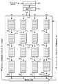
図1は、本発明の一実施例によるシステム100を示すブロック図である。システム100は、命令およびデータを格納するためのシステム・メモリ102と、図形処理のためのグラフィックス処理ユニット104と、外部装置と通信するためのI/Oインターフェース106と、命令およびデータを長期保存するための記憶装置108と、命令およびデータを処理するためのプロセッサ110とを含み得る。A. Exemplary System Overview FIG. 1 is a block diagram illustrating a
本発明の一実施例によれば、プロセッサ110は、1つのL2キャッシュ112および複数のL1キャッシュ116を有し得るし、各L1キャッシュ116は複数のプロセッサ・コア114の1つによって利用される。一実施例によれば、各プロセッサ・コア114はパイプライン化されてもよく、その場合、各命令は一連の小さいステップで遂行され、各ステップは異なるパイプライン・ステージによって遂行される。 According to one embodiment of the present invention,
図2は、本発明の一実施例によるプロセッサ110を示すブロック図である。単純化するために、図2は、プロセッサ110の単一のコア114を示し、そのコア114に関連して説明される。一実施例では、各コア114は同じもの(例えば、同じパイプライン・ステージを有する同じパイプラインを含むもの)であってもよい。別の実施例では、各コア114は異なるもの(例えば、相異なるパイプライン・ステージを有する相異なるパイプラインを含むもの)であってもよい。 FIG. 2 is a block diagram illustrating a
本発明の一実施例では、L2キャッシュ112は、プロセッサ110によって使用される命令およびデータの一部を含み得る。場合によっては、プロセッサ110は、L2キャッシュ112に含まれていない命令およびデータを要求し得る。要求された命令およびデータがL2キャッシュ112に含まれていない場合、その要求された命令およびデータは(より高いレベルのキャッシュまたはシステム・メモリ102のいずれかから)検索され、L2キャッシュ112に収納されてもよい。 In one embodiment of the invention, the
上記ように、場合によっては、L2キャッシュ112は、各々が個別のL1キャッシュ116を使用する1つまたは複数のプロセッサ・コア114によって共有されることもある。一実施例では、プロセッサ110は、1つまたは複数のプロセッサ・コア114およびL1キャッシュ116によって共用される回路をネスト216内に設け得る。従って、所与のプロセッサ・コア114がL2キャッシュ112からの命令を要求するとき、その命令は、先ず、1つまたは複数のプロセッサ・コア114によって共用されるネスト216内のプリレデコーダ兼スケジューラ220によって処理され得る。ネスト216は、更に詳しく後述されるL2キャッシュ・アクセス回路210も含み得るし、その回路216は、共用のL2キャッシュ112をアクセスするために1つまたは複数のプロセッサ・コア114によっても使用されることもある。 As described above, in some cases, the
本発明の一実施例では、命令は、Iラインと呼ばれるグループでL2キャッシュ112からフェッチすることが可能である。同様に、データは、Dラインと呼ばれるグループでL2キャッシュ112からフェッチすることが可能である。図1に示されたL1キャッシュ116は、2つの部分、即ち、Iラインを格納するためのL1命令キャッシュ(Iキャッシュ)222およびDラインを格納するためのL1データ・キャッシュ(Dキャッシュ)224に分割することが可能である。IラインおよびDラインは、L2キャッシュ・アクセス回路210を使用してL2キャッシュ112からフェッチすることが可能である。 In one embodiment of the present invention, instructions can be fetched from
L2キャッシュ112から検索されたIラインは、プリデコーダ兼スケジューラ220によって処理され、Iキャッシュ222に収納されてもよい。プロセッサのパフォーマンスを更に改善するために、命令は、例えば、IラインがL2(または、もっと高レベルの)キャッシュから検索されるとき、および命令がL1キャッシュ116に収納される前に、プリデコードされてもよい。そのようなプリデコーディングは、アドレス生成機能、ブランチ予測機能、および、命令実行を制御するディスパッチ情報(フラッグのセット)として得られるスケジューリング機能(命令が発生されるべき順序を決定する)のような様々な機能を含み得る。例えば、本発明の実施例は、デコーディングがプロセッサにおける別のロケーションで行なわれる場合にも、例えば、命令がL1キャッシュ116から検索された後にデコーディングが行なわれる場合にも使用し得る。 The I line retrieved from the
場合によっては、プリデコーダ兼スケジューラ220は、複数のコア114とL1キャッシュ116との間で共用し得る。同様に、L2キャッシュ112からフェッチされるDラインはDキャッシュ224に収納可能である。各IラインおよびDラインにおける1つのビットは、L2キャッシュ112における情報のラインがIラインまたはDラインのどちらであるかを追跡するためにも使用し得る。任意選択的には、L2キャッシュ112からIラインおよび/またはDラインにおけるデータをフェッチする代わりに、データは、別の方法で、例えば、少量の、多量の、または可変量のデータをフェッチすることによってL2キャッシュ112からフェッチされてもよい。 In some cases, predecoder and
一実施例では、Iキャッシュ222およびDキャッシュ224は、現在どのIラインおよびDラインがIキャッシュ222およびDキャッシュ224にあるかを追跡するために、それぞれ、Iキャッシュ・ディレクトリ223およびDキャッシュ・ディレクトリ225を有し得る。IラインまたはDラインがIキャッシュ222またはDキャッシュ224に加えられるとき、対応するエントリがIキャッシュ・ディレクトリ223またはDキャッシュ・ディレクトリ225に収納される。IラインまたはDラインがIキャッシュ222またはDキャッシュ225から除去されるとき、Iキャッシュ・ディレクトリ223またはDキャッシュ・ディレクトリ225における対応するエントリが除去される。Dキャッシュ・ディレクトリ225を利用するDキャッシュ224に関しては後述されるが、本発明の実施例は、Dキャッシュ・ディレクトリ225が利用されない場合にも利用し得る。そのような場合、Dキャッシュ224自体に格納されたデータは、どのようなDラインがDキャッシュ224に存在するかを表し得る。 In one embodiment, I-cache 222 and D-
一実施例では、コア114のための命令をフェッチするために、命令フェッチ回路236が使用可能である。例えば、命令フェッチ回路236は、コア114において実行されている現在の命令を追跡するプログラム・カウンタを含み得る。ブランチ命令に遭遇するとき、プログラム・カウンタを変更するために、コア114内のブランチ・ユニットが使用可能である。L1Iキャッシュ222からフェッチされた命令を格納するために、Iライン・バッファ232が使用可能である。後述のようにコア114へ並行に送出されるIラインバッファ232における命令を命令グループにグループ化するために、送出キュー234および関連の回路が使用可能である。場合によっては、送出キュー234は、適切な命令グループを形成するためにプリデコーダ兼スケジューラ220によって提供される情報を使用し得る。 In one embodiment, instruction fetch circuit 236 can be used to fetch instructions for
送出キュー234からの命令を受け取ることに加えて、コア114は種々のロケーションからデータを受け取り得る。コア114がデータ・レジスタからのデータを要求する場合、データを得るためにレジスタ・ファイル240が使用可能である。コア114がメモリ・ロケーションからのデータを要求する場合、Dキャッシュ224からデータをロードするために、キャッシュ・ロードおよびストア回路250が使用可能である。そのようなロードが行なわれる場合、必要なデータを求める要求がDキャッシュ224に送出されることが可能である。同時に、所望のデータがDキャッシュ224において見つかったかどうかを決定するために、Dキャッシュ・ディレクトリ225がチェックされる。Dキャッシュ224が所望のデータを含んでいる場合、Dキャッシュ・ディレクトリ225は、Dキャッシュ224が所望のデータを含んでいるということおよびDキャッシュ・アクセスがその後の或る時点で完了し得るということを表す。Dキャッシュ224が所望のデータを含んでいない場合、Dキャッシュ・ディレクトリ225は、Dキャッシュ224が所望のデータを含んでいないということを表す。Dキャッシュ・ディレクトリ225はDキャッシュ224よりも速くアクセスされることが可能であるので、Dキャッシュ・アクセスが完了する前に所望のデータに対する要求を(例えば、L2アクセス回路210を使用して)L2キャッシュ112に送出し得る。 In addition to receiving instructions from the
場合によっては、データがコア114において修正されることもある。修正されたデータは、レジスタ・ファイル240書き込まれるかまたはメモリ102に格納される。データをレジスタ・ファイル240に書き戻すために書き戻し回路238が使用可能である。場合によっては、書き戻し回路238は、データをDキャッシュに書き戻すためにキャッシュ・ロードおよびストア回路250を利用し得る。任意選択的には、コア114が、ストアを行うためにキャッシュ・ロードおよびストア回路250直接アクセスし得る。場合によっては、命令をIキャッシュ222に書き戻すためにも、書き戻し回路238が使用可能である。 In some cases, data may be modified at
上記のように、送出キュー234は、命令グループを形成し且つ形成された命令グループをコア114に送出するために使用し得る。送出キュー234は、Iラインおける命令を回転することおよび組み合せることによって適切な命令グループを形成するための回路も含み得る。送出グループの形成は、送出グループにおける命令相互間の従属性および、更に詳しく後述するように、命令の順序付けから達成することが可能である最適化のような幾つかの事柄を勘案し得る。一旦送出グループが形成されると、その送出グループはプロセッサ・コア114と並行してディスパッチされてもよい。場合によっては、命令グループはコア114における各パイプラインに対して1つの命令を含み得る。任選択的に、命令グループは少数の命令を含み得る。 As described above,
本発明の一実施例によれば、1つまたは複数のプロセッサ・コア114はカスケード型遅延実行パイプライン構成を利用し得る。図3に示される例では、コア114は4つのパイプラインをカスケード型構成で含む。任意選択的には、このような構成において、少数(2つ以上)のパイプライン或いは多数(4つ以上)のパイプラインが使用可能である。更に、図3に示されるパイプラインの物理的なレイアウトは例示的なものであって、必ずしも、カスケード型遅延実行パイプライン・ユニットの実際の物理的なレイアウトを暗示するものではない。 According to one embodiment of the invention, one or
一実施例では、カスケード型遅延実行パイプライン構成における各パイプライン(P0、P1、P2、およびP3)は実行ユニット310を含み得る。実行ユニット310は、所与のパイプラインに対して1つまたは複数の機能を遂行し得る。例えば、実行ユニット310は命令のフェッチおよびデコードのすべて或いは一部分を遂行し得る。実行ユニットによって遂行されるデコードは、複数のコア114の間で共用されるか、または任意選択的に単一のコア114によって利用されるプリデコーダ兼スケジューラ220によって共用されてもよい。実行ユニット310は、レジスタ・ファイル240からデータを読み取り、アドレスを計算し、整数演算機能を(例えば、演算論理ユニット即ちALUを使用して)遂行し、浮動小数点演算機能を遂行し、命令ブランチを実行し、データ・アクセス機能(例えば、メモリからのロードおよびストア)を遂行し、データを(例えば、レジスタ・ファイル240における)レジスタに書き戻すことができる。場合によっては、コア114は、命令フェッチ回路236、レジスタ・ファイル240、キャッシュ・ロードおよびストア回路250、書き戻し回路238、並びにこれらの機能を遂行するための任意の他の回路を利用し得る。 In one embodiment, each pipeline (P0, P1, P2, and P3) in a cascaded delayed execution pipeline configuration may include an execution unit 310. Execution unit 310 may perform one or more functions for a given pipeline. For example, execution unit 310 may perform all or part of instruction fetching and decoding. The decoding performed by the execution unit may be shared among
一実施例では、各実行ユニット310が同じ機能を遂行し得る(例えば、各実行ユニット310がロード/ストア機能を遂行し得る)。任意選択的に、各実行ユニット310(または、実行ユニットの種々のグループ)は種々の機能セットを遂行し得る。更に、場合によっては、各コア114における実行ユニット310は、他のコアに設けられた実行ユニット310と同じであってもよく、またはそれとは異なっていてもよい。例えば、或るコアでは、実行ユニット3100および3102がロード/ストアおよび演算機能を遂行し得るし、一方、実行ユニット3101および3102が演算機能だけを遂行し得る。In one embodiment, each execution unit 310 may perform the same function (eg, each execution unit 310 may perform a load / store function). Optionally, each execution unit 310 (or different groups of execution units) may perform different function sets. Furthermore, depending on the case, the execution unit 310 in each core 114 may be the same as the execution unit 310 provided in the other core, or may be different. For example, in certain cores, execution units 3100 and 3102 may perform load / store and arithmetic functions, while execution units 3101 and 3102 may perform only arithmetic functions.
一実施例では、図示のように、実行ユニット310における実行は、他の実行ユニット310に関して遅延態様でも遂行可能である。図示の構成は、カスケード型遅延構成とも呼ばれることもあるが、図示のレイアウトは、必ずしも、実行ユニットの実際の物理的構成を表すものではない。そのような構成では、命令グループにおける4つの命令(便宜上、I0、I1、I2、I3と呼ばれる)がパイプラインP0、P1、P2、P3に並行して送出される場合、各命令を他の各命令に関して遅延態様で実行することが可能である。それは、例えば、命令I0が、先ず、パイプラインP0に対する実行ユニット3100において実行され、次に、命令I1が、パイプラインP1に対する実行ユニット3101において実行される、等々である。その後、命令I0が実行ユニット3100において実行され終わった後、実行ユニット3100が命令I1を実行し始める、等々となり、従って、コア114に並行して送出された命令が互いに関して遅延態様で実行される。In one embodiment, as shown, execution in execution unit 310 may be performed in a delayed manner with respect to other execution units 310. The illustrated configuration may also be referred to as a cascaded delay configuration, but the illustrated layout does not necessarily represent the actual physical configuration of the execution unit. In such a configuration, if four instructions in an instruction group (referred to as I0, I1, I2, and I3 for convenience) are sent in parallel to the pipelines P0, P1, P2, and P3, each instruction is transferred to each other It is possible to execute in a delayed manner with respect to the instruction. It may, for example, instruction I0 is first executed in the execution unit 3100 with respect to the pipeline P0, then, instruction I1 is executed in the execution unit 3101 for a pipeline P1, and so on. Then, after the instruction I0 has finished being executed in the execution unit 3100, execution unit 3100 starts executing instructions I1, becomes so, therefore, execution command sent in parallel to the
一実施例では、或る実行ユニット310は互いに関して遅延し得るし、一方、他の実行ユニット310は互いに関して遅延し得ない。第2命令の実行が第1命令の実行に従属する場合、転送パス312は、第1の命令から第2の命令に結果を転送するために使用可能である。図示の転送パス312は単に例示的なものであり、コア114は、実行ユニット310における種々のポイントから他の実行ユニット310への、或いは同じ実行ユニット310への、更なる転送パスを有してもよい。 In one embodiment, some execution units 310 may be delayed with respect to each other while other execution units 310 may not be delayed with respect to each other. If the execution of the second instruction is dependent on the execution of the first instruction, the
一実施例では、実行ユニット310によって実行されていない命令は、遅延キュー320またはターゲット遅延キュー330に保持されることが可能である。遅延キュー320は、実行ユニット310によって実行されていない命令グループにおける命令を保持するために使用可能である。例えば、命令I0が実行ユニット3100において実行されている間、命令I1、I2、およびI3は遅延キュー330に保持されることが可能である。一旦命令が遅延キュー330を通過してしまうと、その命令は適切な実行ユニット310に送出され、実行されることが可能である。ターゲット遅延キュー330は、実行ユニット310によって既に実行された命令の結果を保持するために使用し得る。場合によっては、ターゲット遅延キュー330における結果が処理のために実行ユニット310に転送され、それの無効化が適切である場合には無効化される。同様に、状況によっては、後述のように遅延キュー320における命令を無効化することも可能である。In one embodiment, instructions that are not being executed by execution unit 310 may be held in
一実施例では、命令グループにおける命令の各々が遅延キュー320、実行ユニット310、およびターゲット遅延キュー330を通過した後、その結果(例えば、データ、および、後述のように、命令)がレジスタ・ファイル或いはL1Iキャッシュ222、および/または、Dキャッシュ224のいずれかに書き戻されることがある。場合によっては、レジスタの最近修正された値を書き戻し且つ無効化された結果を廃棄するために書き戻し回路306を使用してもよい。 In one embodiment, after each instruction in the instruction group passes through
B.キャッシュ・メモリのアクセス
本発明の一実施例では、各プロセッサ・コア114に対するL1キャッシュ116は、有効アドレスを使用してアクセスされ得る。L1キャッシュ116が個別のL1Iキャッシュ222およびL1Dキャッシュ224を使用する場合、キャッシュ222および224の各々も有効アドレスを使用してアクセスされ得る。場合によっては、プロセッサ・コア114による命令の実行により直接与えられる有効アドレスを使ってL1キャッシュ116をアクセスすることによって、アドレス変換により生じた処理オーバーヘッドはL1キャッシュ・アクセス中に除去され、それによって、プロセッサ・コア114がL1キャッシュ116をアクセスする速度を増加させ、消費電力を減少させ得る。B. Cache Memory Access In one embodiment of the invention, the
場合によっては、複数のプログラムが、種々のデータをアクセスするために同じ有効アドレスを使用し得る。例えば、第1プログラムは、第1実アドレスRA1に対応するデータをアクセスするために第1有効アドレスEA1が使用される、ということを表す第1アドレス変換を使用し得る。第2のプログラムは、EA1が第2実アドレスRA2をアクセスするために使用される、ということを表すために第2アドレス変換を使用し得る。各プログラムに対して種々のアドレス変換を使用することによって、プログラムの各々に対する有効アドレスは、大きい実アドレス空間における種々の実アドレスに変換され、それによって、種々のプログラムが間違ったデータを不注意にアクセスすることを防ぐことが可能である。アドレス変換は、例えば、システム・メモリ102におけるページ・テーブルおいて維持されてもよい。プロセッサ110によって使用されるアドレス変換の部分は、例えば、変換ルックアサイド・バッファまたはセグメント・ルックアサイド・バッファのようなルックアサイド・バッファにおいてキャッシュすることが可能である。 In some cases, multiple programs may use the same effective address to access different data. For example, the first program may use a first address translation that indicates that the first effective address EA1 is used to access data corresponding to the first real address RA1. The second program may use the second address translation to indicate that EA1 is used to access the second real address RA2. By using different address translations for each program, the effective address for each of the programs is translated into different real addresses in a large real address space, so that different programs inadvertently misplace the wrong data. It is possible to prevent access. Address translation may be maintained, for example, in a page table in
場合によっては、有効アドレスを使用してL1キャッシュ116におけるデータがアクセスされてもよいので、同じ有効アドレスを使用する種々のプログラムが間違ったデータを不注意にアクセスしないようにするという要望がある。例えば、第1プログラムがL1キャッシュ116をアクセスするためにEA1、即ち、第2プログラムによっても使用されるRA2と呼ぶべきアドレス、を使用する場合、第1プログラムは、RA2に対応するデータではなくRA1に対応するデータをL1キャッシュ116から受け取らなければならない。 In some cases, data in the
従って、本発明の一実施例では、プロセッサ110は、コア114に対してL1キャッシュ116をアクセスするためにプロセッサ110のコア114において使用されている各有効アドレスに対して、L1キャッシュ116におけるデータが、実行されているプログラムによって使用されるアドレス変換のための正しいデータである、ということを保証することができる。従って、有効アドレスEA1が実アドレスRA1に変換するということを表す第1プログラムに対するエントリを、プロセッサ110によって使用されるルックアサイド・バッファが含む場合、プロセッサ110は、有効アドレスEA1を有するとしてマークされたL1キャッシュ116におけるいずれのデータも実アドレスRA1に格納された同じデータである、ということを保証し得る。EA1に対するアドレス変換エントリがルックアサイド・バッファから除去される場合、対応するデータは、それが存在すれば、L1キャッシュ116から取り除かれ、それによって、L1キャッシュ116におけるデータがすべてルックアサイド・バッファに有効な変換エントリを有する、ということことを保証することができる。アドレス変換のために使用されるルックアサイド・バッファにおける対応するエントリによりL1キャッシュ116におけるすべてのデータがマップされる、ということを保証することによって、L1キャッシュ116は、所与のプログラムがL1キャッシュ116からの間違ったデータを不注意に受け取ることを防ぐと同時に、有効アドレスを使用してアクセスされることが可能である。 Thus, in one embodiment of the present invention,
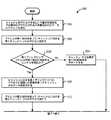
図4は、本発明の一実施例に従ってL1キャッシュ116(例えば、Dキャッシュ224)をアクセスするためのプロセス400を示すフローチャートである。プロセス400が開始すると、ステップ402において、アクセスされるべきデータの有効アドレスを含むアクセス命令が受け取られる。アクセス命令は、プロセッサ・コア114が受け取るロード命令或いはストア命令であってもよい。ステップ404において、アクセス命令は、プロセッサ・コア114により、例えば、ロード・ストア機能を有する実行ユニット310の1つにおいて実行される。 FIG. 4 is a flowchart illustrating a
ステップ406において、プロセッサ・コア114に対するL1キャッシュ116が、アクセス命令の有効アドレスに対応するデータを含むかどうかを決定するために、そのアクセス命令の有効アドレスはアドレス変換なしで使用されることが可能である。ステップ408において、L1キャッシュ116が有効アドレスに対応するデータを含むという決定が行われる場合、ステップ410において、そのアクセスのためのデータがL1キャッシュ116から提供される。しかし、ステップ408において、L1キャッシュ116がそのデータを含まないという決定が行われる場合、ステップ412において、有効アドレスに対応するデータを検索する要求がL2キャッシュ・アクセス回路210に送られる。L2キャッシュ・アクセス回路210は、例えば、L2キャッシュ112からデータをフェッチするか、またはより高いレベルのキャッシュ・メモリ階層から、例えば、システム・メモリ102からデータを検索し、その検索されたデータをL2キャッシュ112に収納し得る。次に、ステップ414において、そのアクセス命令に対するデータがL2キャッシュ112から提供されることが可能である。 In
図5は、本発明の一実施例に従って、有効アドレスを使用してL1Dキャッシュ224にアクセスするための回路を示すブロック図である。上記のように、本発明の実施例は、統合されたL1キャッシュ116或いはL1Iキャッシュ222が有効アドレスによってアクセスされる場合にも使用し得る。一実施例では、L1Dキャッシュ224が、バンク0 502およびバンク1 504のような複数のバンクを含み得る。L1Dキャッシュ224は、例えば、L1Dキャッシュ224に適用されたロード・ストア有効アドレス(LS0、LS1、LS2、LS3)に従って2つの4倍長ワードまたは4つの2倍長ワード(DW0、DW1、DW0’、DW1’)を読取るために使用することができる複数のポートを含み得る。L1Dキャッシュ224は、ダイレクト・マップされたセット・アソシエイティブ・キャッシュまたは完全アソシエイティブ・キャッシュであってもよい。 FIG. 5 is a block diagram illustrating a circuit for accessing the
一実施例では、Dキャッシュ・ディレクトリ225は、L1Dキャッシュ224をアクセスするために使用することが可能である。例えば、要求されたデータに対する有効アドレスEAがディレクトリ225に提供されることがある。ディレクトリ225もダイレクト・マップされたセット・アソシエイティブ・キャッシュまたは完全アソシエイティブ・キャッシュであってもよい。ディレクトリ225がアソシエイティブである場合、有効アドレスの一部分(EA SEL)は、要求されたデータに関する情報にアクセスするために、ディレクトリ225に対する選択回路510によって使用されてもよい。ディレクトリ225が、要求されたデータの有効アドレスに対応するエントリを含んでいない場合、ディレクトリ225は、例えば、より高いレベルのキャッシュ階層から(例えば、L2キャッシュ112或いはシステム・メモリ102から)データを要求するために使用されるミス信号をアサートし得る。しかし、ディレクトリ225が、要求されたデータの有効アドレスに対応するエントリを含んでいる場合、エントリは、要求されたデータを提供するためにL1Dキャッシュ224の選択回路506および508によって使用されることが可能である。 In one embodiment, D-
本発明の一実施例では、L1キャッシュ116、L1Dキャッシュ224、および/または、L1Iキャッシュ222もスプリット・キャッシュ・ディレクトリを使用してアクセスされることが可能である。例えば、キャッシュ・ディレクトリへのアクセスを分割することによって、ディレクトリへのアクセスはより速く行なわれ、それによって、キャッシュ・メモリ・システムをアクセスするときにプロセッサ110のパフォーマンスを改善し得る。有効アドレスによってキャッシュをアクセスすることに関して説明したが、スプリット・キャッシュ・ディレクトリは、任意のタイプのアドレス(例えば、実アドレスまたは有効アドレス)によってアクセスされる任意のキャッシュ・レベル(例えば、L1、L2等)を用いて使用されてもよい。 In one embodiment of the present invention,
図6および図7は、本発明の一実施例に従って、スプリット・ディレクトリを使用してキャッシュにアクセスするためのプロセス600を示すフローチャートである。プロセス600が開始すると、ステップ602において、キャッシュをアクセスする要求が受け取られる。要求は、アクセスされるべきデータのアドレス(例えば、実アドレスまたは有効アドレス)を含み得る。次に、ステップ604において、そのアドレスの第1部分(例えば、上位桁ビットまたは下位桁ビット)が、キャッシュに対する第1ディレクトリへのアクセスを行うために使用される。第1ディレクトリはアドレスの一部分を用いてアクセスすることが可能であるので、第1ディレクトリのサイズは縮小され、それによって、第1ディレクトリがより大きいディレクトリよりも速くアクセスされることを可能にする。 6 and 7 are flowcharts illustrating a
ステップ620において、第1ディレクトリが、要求されたデータのアドレスの第1部分に対応するエントリを含んでいるかどうか、に関する決定が行われる。ディレクトリが第1部分に対するエントリを含んでいないという決定が行われる場合、ステップ624において、キャッシュ・ミスを表す第1信号をアサートすることが可能である。キャッシュ・ミスを表す第1信号を検知したことに応答して、ステップ628において、要求されたデータをフェッチするという要求がより高いレベルのキャッシュ・メモリに送られる。上記のように、第1ディレクトリが小さく且つ大きいディレクトリより速くアクセスされ得るので、キャッシュ・ミスを表す第1信号をアサートし、より高いレベルのキャッシュからメモリをフェッチし始めるべきであるかどうかに関するの決定をより速く行うことができる。第1ディレクトリに対するアクセス・タイムが短いために、第1信号は早期ミス信号とも呼ばれ得る。 At
第1ディレクトリが第1部分に対するエントリを含んでいる場合、ステップ608において、第1ディレクトリへのアクセスからの結果を使用してキャッシュからのデータを選択することが可能である。上記のように、第1ディレクトリは小さく且つ大きなディレクトリより速くアクセスされるので、キャッシュからのデータの選択はより速く行うことが可能である。従って、キャッシュ・アクセスは、大きい統合ディレクトリを利用するシステムの場合よりも速く完了し得る。 If the first directory contains an entry for the first portion, in
場合によっては、アドレスの一部分(例えば、アドレスの上位桁ビット)を使用して、キャッシュからのデータの選択が行なわれるので、キャッシュから選択されたデータは、実行されているプログラムによって要求されたデータと一致しないことがある。例えば、2つのアドレスが同じ上位桁ビットを持つことがあり得るが、下位桁ビットは異なることがある。選択されたデータが、要求されたデータに対するアドレスの下位桁ビットとは異なる下位桁ビットを有するアドレスを持つ場合、選択されたデータは要求されたデータと一致し得ない。従って、場合によっては、選択されたデータがその要求されたデータであるという高い確率は存在するが、それの絶対的な確信は存在しないので、キャッシュからのデータの選択は推測的なものであると考えることができる。 In some cases, selection of data from the cache is performed using a portion of the address (eg, the upper digit bits of the address) so that the data selected from the cache is the data requested by the program being executed. May not match. For example, two addresses can have the same high order bits, but the low order bits can be different. If the selected data has an address with a lower digit bit that is different from the lower digit bit of the address for the requested data, the selected data cannot match the requested data. Thus, in some cases, there is a high probability that the selected data is the requested data, but there is no absolute belief in it, so the selection of data from the cache is speculative. Can be considered.
一実施例では、正しいデータがキャッシュから選択されたということを確認するために、キャッシュに対する第2ディレクトリを使用してもよい。例えば、第2ディレクトリは、ステップ610において、アドレスの第2部分を用いてアクセスすることが可能である。ステップ622において、第2ディレクトリが、第1ディレクトリからのエントリと一致するアドレスの第2部分に対応するエントリを含んでいるかどうかに関する決定が行われる。例えば、第1ディレクトリおよび第2ディレクトリにおけるエントリはタグを付加されてもよく、或いは各ディレクトリにおける対応するロケーションに格納されてもよく、それによって、アドレスの第1部分およびアドレスの第2部分を含む単一の一致アドレスにそのエントリが対応するということを表す。 In one embodiment, a second directory for the cache may be used to confirm that the correct data has been selected from the cache. For example, the second directory can be accessed at
第2ディレクトリがアドレスの第2部分に対応する一致エントリを含んでいない場合、ステップ626において、キャッシュ・ミスを表す第2信号がアサートされてもよい。上記第1信号がアサートされないときでも、第2信号がアサートされるので、第2信号は遅延キャッシュ・ミス信号と呼ばれることもある。ステップ628において、要求されたデータをL2キャッシュ112のような高いレベルのキャッシュ・メモリからフェッチするという要求を送るために、第2信号を使用することも可能である。第2信号は、誤って選択されたデータが、別のメモリ・ロケーションに格納されること、レジスタに格納されること、またはオペレーションにおいて使用されることを防ぐために使用されてもよい。ステップ630において、要求されたデータが高いレベルのキャッシュ・メモリから提供される。 If the second directory does not contain a matching entry corresponding to the second portion of the address, then at
第2ディレクトリがアドレスの第2部分に対応する一致したエントリを含んでいる場合、ステップ614において第3信号がアサートされる。第3信号は、第1ディレクトリを使用して選択されたデータが要求されたデータと一致するということを確認し得る。ステップ616では、キャッシュ・アクセス要求に対する選択されたデータをキャッシュから供給することが可能である。例えば、選択されたデータは、演算オペレーションにおいて使用され、別のメモリ・アドレスに格納され、或いはレジスタに格納されてもよい。 If the second directory contains a matched entry corresponding to the second part of the address, then at step 614, a third signal is asserted. The third signal may confirm that the data selected using the first directory matches the requested data. In
図6および図7に示され且つ上述されたプロセス600のステップに関して、提供された順序は単に例示的なものである。一般に、それらのステップは任意の適切な順序で遂行されてもよい。例えば、選択されたデータは、第1ディレクトリがアクセスされた後で、且つその選択が第2ディレクトリによって確認される前に、提供される。選択され且つ提供されたデータが要求されたデータではないということを第2ディレクトリが表す場合、その後のステップは、当業者には明らかなように、推測的に選択されたデータを用いて遂行されたすべてのアクションを取消すために行われる。更に、場合によっては、第2ディレクトリは第1ディレクトリの前にアクセスされてもよい。 With respect to the steps of the
場合によっては、上記のように、複数のアドレスが同じ上桁ビットまたは下位桁ビットを有することがある。従って、第1ディレクトリは、アドレスの所与の部分(例えば、第1ディレクトリおよび第2ディレクトリの構成の仕方次第で上位桁ビットまたは下位桁ビット)と一致する複数のエントリを有することがある。一実施例では、第1ディレクトリが、要求されたデータに対するアドレスの所与の部分と一致する複数のエントリを含んでいる場合、第1ディレクトリからエントリの1つが選択され、キャッシュからデータを選択するために使用される。例えば、第1ディレクトリにおける複数のエントリのうちの最近使用されたエントリがキャッシュからデータを選択するために使用されてもよい。その選択は、要求されたデータのアドレスに対する正しいエントリが使用されたかどうかを決定するために後で確認されてもよい。 In some cases, as described above, multiple addresses may have the same upper or lower digit bits. Thus, the first directory may have multiple entries that match a given portion of the address (eg, upper or lower digit bits depending on how the first and second directories are configured). In one embodiment, if the first directory includes multiple entries that match a given portion of the address for the requested data, one of the entries from the first directory is selected to select the data from the cache. Used for. For example, a recently used entry of the plurality of entries in the first directory may be used to select data from the cache. The selection may be verified later to determine if the correct entry for the requested data address has been used.
第1ディレクトリからのエントリの選択が正しくなかった場合、1つまたは複数の他のエントリがキャッシュからデータを選択するために使用されてもよく、その1つまたは複数の他のエントリは、それが、要求されたデータに対するアドレスと一致するかどうかを決定するために使用されてもよい。第1ディレクトリにおける他のエントリの1つが要求されたデータに対するアドレスと一致し、更に第2ディレクトリからの対応するエントリを用いて確認される場合、その選択されたデータは、その後のオペレーションにおいて使用することが可能である。第1ディレクトリにおけるいずれのエントリも第2ディレクトリにおけるエントリと一致しない場合、キャッシュ・ミスが信号され、データがより高いレベルのキャッシュ・メモリ階層からフェッチされる。 If the entry selection from the first directory was incorrect, one or more other entries may be used to select data from the cache, and the one or more other entries May be used to determine if it matches the address for the requested data. If one of the other entries in the first directory matches the address for the requested data and is further confirmed using the corresponding entry from the second directory, the selected data is used in subsequent operations. It is possible. If any entry in the first directory does not match the entry in the second directory, a cache miss is signaled and the data is fetched from a higher level cache memory hierarchy.
図8は、本発明の一施例に従って、第1Dキャッシュ・ディレクトリ702および第2Dキャッシュ・ディレクトリ712を含むスプリット・キャッシュ・ディレクトリを示すブロック図である。一実施例では、第1Dキャッシュ・ディレクトリ702は有効アドレスの上位桁ビット(EA上位)を用いてアクセスされ、一方、第2Dキャッシュ・ディレクトリ712は有効アドレスの下位桁ビット(EA下位)を用いてアクセスされる。上述したように、実施例は、第1Dキャッシュ・ディレクトリ702および第2 Dキャッシュ・ディレクトリ712が実アドレスを使ってアクセスされる場合にも使用し得る。第1および第2Dキャッシュ・ディレクトリ702および712は、ダイレクト・マップ・ディレクトリ、セット・アソシエイティブ・ディレクトリ、またはフル・アソシエイティブ・ディレクトリであってもよい。ディレクトリ702および712は、それぞれのディレクトリ702および712からデータ・エントリを選択するために使用される選択回路704および714を含み得る。 FIG. 8 is a block diagram illustrating a split cache directory that includes a first
上述したように、L1Dキャッシュ224へのアクセス中、そのアクセスのためのアドレスの第1部分(EA上位)は第1Dキャッシュ・ディレクトリ702をアクセスするために使用される。第1Dキャッシュ・ディレクトリ702がそのアドレスに対応するエントリを含んでいる場合、そのエントリは、選択回路506および508を介してL1Dキャッシュ224をアクセスするために使用することが可能である。第1Dキャッシュ・ディレクトリ702がそのアドレスに対応するエントリを含んでいない場合、早期ミス信号と呼ばれるミス信号が上述のようにアサートされる。早期ミス信号は、例えば、高いレベルのキャッシュ・メモリ階層からのフェッチを開始するために、および/または、キャッシュ・ミスを表す例外を生成するために使用されてもよい。 As described above, during access to the
アクセス中に、アクセスのためのアドレスの第2部分(EA下位)は第2Dキャッシュ・ディレクトリ712をアクセスするために使用されてもよい。そのアドレスに対応する第2Dキャッシュ・ディレクトリ712からのいずれのエントリも、比較回路720を使って第1Dキャッシュ・ディレクトリ720からのエントリと比較される。第2Dキャッシュ・ディレクトリ712がそのアドレスに対応するエントリを含んでいない場合、または、第2Dキャッシュ・ディレクトリ712からのエントリが第1Dキャッシュ・ディレクトリ702からのエントリと一致しない場合、遅延ミス信号とも呼ばれるミス信号がアサートされる。しかし、第2Dキャッシュ・ディレクトリ712がそのアドレスに対応するエントリを含んでいる場合、および、第2Dキャッシュ・ディレクトリ712からのエントリが第1Dキャッシュ・ディレクトリ702からのエントリと一致する場合、L1キャッシュ224からの選択されたデータが要求されたデータのアドレスに対応するということを表す選択確認信号と呼ばれる信号をアサートすることが可能である。 During access, the second part of the address for access (EA subordinate) may be used to access the second D-
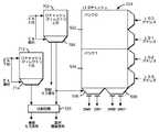
図9は、本発明の一実施例に従ってキャッシュ・アクセス回路を示すブロック図である。上述のように、要求されたデータがL1キャッシュ116に収納されていない場合、そのデータを求める要求がL2キャッシュ112に送られる。更に、場合によっては、プロセッサ110は、例えば、プロセッサ110によって実行されているプログラムの予測された実行パスに基づいて、L1キャッシュ116に命令をプリフェッチするように構成されてもよい。従って、L2キャッシュ112は、データがプリフェッチされてL1キャッシュ116に入れられることを求める要求を受け取ることもある。 FIG. 9 is a block diagram illustrating a cache access circuit according to one embodiment of the present invention. As described above, if the requested data is not stored in the
一実施例では、L2キャッシュ112からのデータを求める要求をL2キャッシュ・アクセス回路210が受け取ることもある。上述のように、本発明の一実施例では、プロセッサ・コア114およびL1キャッシュ116は、そのデータに対する有効アドレスを使用してデータをアクセスするように構成されてもよく、一方、L2キャッシュ112はデータに対する実アドレスを使用してアクセスされてもよい。従って、L2キャッシュ・アクセス回路210は、コア114から受け取った有効アドレスを実アドレスに変換するように構成されるアドレス変換制御回路806を含み得る。例えば、そのアドレス変換制御回路は、変換を行うためにセグメント・ルックアサイド・バッファ802、および/または、変換ルックアサイド・バッファ804におけるエントリを使用し得る。アドレス変換制御回路806が、受け取った有効アドレスを実アドレスに変換した後、その実アドレスは、L2キャッシュ112をアクセスするために使用することができる。 In one embodiment, the L2
上述のように、本発明の一実施例では、プロセッサ・コア114によって実行されているスレッドが、データの有効アドレスを使用すると同時に正しいデータをアクセスするということを保証するために、プロセッサ110は、L1キャッシュ116におけるすべての有効データ・ラインがSLB802、および/または、TLB804における有効なエントリによってマップされるということを保証し得る。従って、エントリがルックアサイド・バッファ802および804の1つからキャスト・アウトされるかまたはその1つにおいて無効にされるとき、アドレス変換制御回路806は、それぞれのルックアサイド・バッファ802、804からのラインの有効アドレスを提供する(EAを無効にする)ように、および、データ・ラインが存在する場合には、そのデータ・ラインがL1キャッシュ116および/またはL1キャッシュ・ディレクトリから(例えば、Iキャッシュ・ディレクトリ223および/またはDキャッシュ・ディレクトリ225から)除去されなければならないということを表す無効化信号を提供するように、構成することが可能である。 As described above, in one embodiment of the present invention, to ensure that the thread executing by
一実施例では、プロセッサ110は、それぞれのL1キャッシュ116をアクセスするのためのアドレス変換を使用しない複数のコア114を含み得るので、コア114がアドレス変換を行った場合に生じるエネルギ消費は減少し得る。更に、アドレス変換制御回路806および他のL2キャッシュ・アクセス回路210が、アドレス変換を行うためにコア114の各々によって共用され、それによって、L2キャッシュ・アクセス回路210によって消費されるチップ・スペースの点から(例えば、L2キャッシュ112がコア114と同じチップ上に設けられる場合)、オーバヘッドの量を減らし得る。 In one embodiment, the
一実施例では、L2キャッシュ・アクセス回路210、および/または、プロセッサ110のコア114によって共用されるネスト216内の他の回路を、コア114の頻度より低い頻度で操作することが可能である。従って、例えば、ネスト216における回路は、オペレーションを遂行するために第1クロック信号を使用し得るし、一方、コア114における回路はオペレーションを遂行するために第2クロック信号を使用し得る。第1クロック信号は第2クロック信号の周波数より低い周波数を有することがある。コア114における回路よりも低い周波数でネスト216における共用の回路を操作することによって、プロセッサ110の電力消費量は減少し得る。ネスト216における操作回路は、L2キャッシュ・アクセス・タイムを増加させることがあるが、アクセス・タイム全体の増加は、L2キャッシュ112に対する典型的な合計アクセス・タイムに比べてかなり小さくなり得る。 In one embodiment, the L2
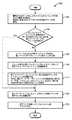
図10は、本発明の一実施例に従ってキャッシュ・アクセス回路210を使用して、L2キャッシュ112をアクセスするプロセス900を示すフローチャートである。プロセス900が開始すると、ステップ902において、要求されたデータをL2キャッシュ112からフェッチする要求が受け取られる。その要求は、要求されたデータに対する有効アドレスを含み得る。ステップ904において、ルックアサイド・バッファ(例えば、SLB802および/またはTLB804)がその要求されたデータの有効アドレスに対するエントリを含むかどうかに関する決定が行なわれる。 FIG. 10 is a flowchart illustrating a
ステップ904において、ルックアサイド・バッファ802および804がその要求されたデータの有効アドレスに対する第1ページ・テーブル・エントリを含んでいるかどうかに関する決定が行われる。ルックアサイド・バッファ802および804がその要求されたデータの有効アドレスに対するページ・テーブル・エントリを含んでいる場合、ステップ920において、第1ページ・テーブル・エントリが有効アドレスを実アドレスに変換するために使用される。しかし、ステップ906では、ルックアサイド・バッファ802および804が要求されたデータの有効アドレスに対するページ・テーブル・エントリを含んでいる場合、第1ページ・テーブル・エントリが、例えば、システム・メモリ102におけるページ・テーブルからフェッチされる。 In
場合によっては、新しいページ・テーブル・エントリがシステム・メモリ102からフェッチされ、ルックアサイド・バッファ802、804に収納されるとき、その新しいページ・テーブル・エントリはルックアサイド・バッファ802および804における古いエントリを置換し得る。従って、古いページ・テーブル・エントリが置換される場合、その置換されたエントリに対応するL1キャッシュ116におけるいずれのキャッシュ・ラインも、L1キャッシュ116をアクセスするプログラムが正しいデータをアクセスすることを保証するためにL1キャッシュ116から取り除かれる。従って、ステップ908において、第2ページ・テーブル・エントリがフェッチされた第1ページ・テーブル・エントリと置換される。 In some cases, when a new page table entry is fetched from
ステップ910において、第2ページ・テーブル・エントリに対する有効アドレスがL1キャッシュ116に供給され、それは、第2のページ・テーブル・エントリに対応するいずれのデータもL1キャッシュ116からフラッシュおよび/または無効化されなければならない、ということを表す。上述したように、TLB804および/またはSLB802にマップされてないL1キャッシュ・ラインをフラッシュおよび/または無効化することによって、プロセッサ・コア114によって実行されるプログラムは、有効アドレスを用いて正しくないデータを不注意にアクセスすることを防ぐことができる。場合によっては、ページ・テーブル・エントリが複数のL1キャッシュ・ラインを指すこともある。更に、場合によっては、単一のSLBエントリは、複数のL1キャッシュ・ラインを含む複数のページを指すこともある。そのような場合、L1キャッシュから除去されるべきページの表示がプロセッサ・コア114に送られ、その表示されたページに対応する各キャッシュ・ラインがL1キャッシュ116から除去される。更に、L1キャッシュ・ディレクトリ(またはスプリット・キャッシュ・ディレクトリ)が利用される場合、表示されたページに対応するL1キャッシュ・ディレクトリにおけるいずれのエントリも除去される。ステップ920において、第1ページ・テーブル・エントリがルックアサイド・バッファ802、804内にある場合、第1ページ・テーブル・エントリは要求されたデータの有効アドレスを実アドレスに変換するために使用される。しかる後、ステップ922において、その変換から得られた実アドレスは、L2キャッシュ112をアクセスするために使用することが可能である。 In
一般に、上述された本発明の実施例は、任意の数のプロセッサ・コアを備えた任意のタイプのプロセッサを用いて使用することが可能である。複数のプロセッサ・コア114が使用される場合、L2キャッシュ・アクセス回路210は各プロセッサ・コア114に対してアドレス変換を行い得る。従って、エントリがTLB804またはSLB802からキャスト・アウトされるとき、いずれの対応するキャッシュ・ラインもL1キャッシュ116から除去されなければならないということを表す信号を、プロセッサ・コア114に対するL1キャッシュ116の各々に送ることができる。 In general, the embodiments of the present invention described above can be used with any type of processor with any number of processor cores. When
図11は、例示的な設計フロー1000のブロック図を示す。設計フロー1000は、設計されるICのタイプに依存して変り得る。例えば、特定用途向けIC(ASIC)を形成するための設計フロー1000は、標準的なコンポーネントを設計するための設計フローとは異なることがある。設計構造体1020は、設計プロセス1010への入力であることが望ましく、IP提供者、中心的開発者、または他の設計会社から提供されたり、或いは設計フローの担当者によってまたは他のソースから生成されたりすることも可能である。設計構造体1020は、図形的概略図またはHDL即ちハードウェア記述言語(例えば、Verilog、VHDL,C等)の形式の上述の回路、並びに図1〜図3、図5、図8、および図9に示された回路を含む。設計構造体1020は、1つまたは複数のマシン可読媒体上に含まれてもよい。例えば、設計構造体1020は、テキスト・ファイルであってもよく、上述の回路、並びに図1〜図3、図5、図8、および図9に示された回路の図形的表示であってもよい。設計プロセス1010は、上述の回路、並びに図1〜図3、図5、図8、および図9に示された回路をネットリスト1080の形に合成することが望ましい。なお、ネットリスト1080は、例えば、ワイヤ、トランジスタ、論理ゲート、制御回路、I/O、モデル等に関するリストであり、集積回路設計において他の素子および回路への接続を記述し、少なくとも1つのマシン可読媒体上に記録される。例えば、その媒体は、CD、コンパクト・フラッシュ・メモリ、他のフラッシュ・メモリ、またはハードディスク・ドライブのような記憶媒体であってもよい。その媒体は、インターネットまたは他のネットワーキングに適した手段を介して送られるべきデータのパケットであってもよい。合成は、その回路のための設計仕様およびパラメータに従ってネットリスト1080が1回または複数回再合成される、反復性のプロセスであってもよい。 FIG. 11 shows a block diagram of an
設計プロセス1010は、種々の入力を使用して、例えば、所与の製造技術(例えば、種々の技術ノード、32nm、45nm、90nm等)のためのモデル、レイアウト、および記号表示を含む共通使用の素子、回路、および装置のセットを内蔵し得るライブラリ素子1030、設計仕様1040、特徴付けデータ1050、検証データ1060、設計ルール1070、およびテスト・データ・ファイル1085(テスト・パターンおよび他の試験情報を含み得る)からの入力の使用を含み得る。更に、設計プロセス1010は、例えば、タイミング分析、検証、設計ルール・チェック、設置、および経路指定オペレーション等のような標準的な回路設計プロセスを含み得る。集積回路設計の当業者は、本発明の技術的範囲および主旨から逸脱することなく設計プロセス1010において使用される可能な電子的設計自動化ツールおよびアプリケーションの範囲を十分理解し得るであろう。本発明の設計構造体はいずれの特定の設計フローにも限定されない。 The
設計プロセス1010は、上述の回路並びに図1〜図3、図5、図8、および図9に示された回路を、任意の更なる集積回路設計またはデータ(適用可能であれば)と共に第2の設計構造体1090に変換することが望ましい。設計構造体1090は、集積回路のレイアウト・データ(例えば、GDSII(GDS2)に保存された情報、GL1、OASIS、または、そのような設計構造体を保存するに適した任意の他のフォーマット)の交換のために使用されるデータ・フォーマットで記憶媒体上に存在する。設計構造体1090は、例えば、テスト・データ・ファイル、設計内容ファイル、製造データ、レイアウト・パラメータ、ワイヤ、金属のレベル、バイアス、形状、製造ラインを通すためのデータ、および、上述の回路並びに図1〜図3、図5、図8、および図9に示された回路を製作するために半導体製造者が必要とする他の任意のデータ、のような情報を含み得る。設計構造体1090は、次に、ステージ1095に進む。ステージ1095では、例えば、設計構造体1090は、テープ・アウトに進み、製造にリリースされ、マスク・ハウスにリリースされ、他の設計ハウスに送られ、顧客に返送される等であってもよい。 The
以上は本発明の実施例に関するものであるが、本発明の他のおよび更なる実施例が、その基本的な範囲から逸脱することなく考えられ得る。 While the above is directed to embodiments of the invention, other and further embodiments of the invention may be devised without departing from the basic scope thereof.
Claims (22)
Translated fromJapanese前記プロセッサの1つまたは複数のレベル1キャッシュにおける要求されたデータを、前記要求されたデータの要求された有効アドレスを使用してアクセスするステップと、
前記プロセッサの1つまたは複数のレベル1キャッシュが前記要求された有効アドレスに対応する要求されたデータを含んでいない場合、前記要求された有効アドレスを実アドレスに変換するステップであって、前記プロセッサの1つまたは複数のレベル1キャッシュの各々における各キャッシュ・ラインに対してルックアサイド・バッファが1つの対応するエントリを含み、前記対応するエントリが前記キャッシュ・ラインに対して前記有効アドレスから前記実アドレスへの変換を表す、前記変換するステップと、
レベル2キャッシュをアクセスするために、前記変換するステップにおいて変換された実アドレスを使用するステップと、
を含む、方法。A method of accessing cache memory in a processor, comprising:
Accessing requested data in one or more level 1 caches of the processor using a requested effective address of the requested data;
If the one or more level 1 caches of the processor do not contain the requested data corresponding to the requested effective address, converting the requested effective address to a real address, the processor A look-aside buffer for each cache line in each of the one or more level 1 caches includes a corresponding entry, the corresponding entry for the cache line from the effective address to the real address. Said converting step representing a conversion to an address;
Using the real address translated in the translating step to access the level 2 cache;
Including a method.
レベル2キャッシュと、
ルックアサイド・バッファと、
回路と、
を含み、前記回路は、
前記1つまたは複数のレベル1キャッシュにおける要求されたデータを、前記要求されたデータの要求された有効アドレスを使用してアクセスし、
前記1つまたは複数のレベル1キャッシュが前記要求された有効アドレスに対応する要求されたデータを含んでいない場合、前記要求された有効アドレスを実アドレスに変換し、前記1つまたは複数のレベル1キャッシュの各々における各キャッシュ・ラインに対してルックアサイド・バッファが、前記キャッシュ・ラインに対して前記有効アドレスから前記実アドレスへの変換を表す1つの対応するエントリを含み、
前記レベル2キャッシュをアクセスするために、変換された実アドレスを使用する、
ように構成される、プロセッサ。One or more level 1 caches;
Level 2 cache,
A lookaside buffer;
Circuit,
The circuit includes:
Accessing requested data in the one or more level 1 caches using a requested effective address of the requested data;
If the one or more level 1 caches do not contain the requested data corresponding to the requested effective address, the requested effective address is converted to a real address and the one or more level 1 A lookaside buffer for each cache line in each of the caches includes one corresponding entry representing a translation from the effective address to the real address for the cache line;
Use the translated real address to access the level 2 cache;
Configured as a processor.
プロセッサと、
を含み、前記プロセッサは、
1つまたは複数のレベル1キャッシュと、
前記1つまたは複数のレベル1キャッシュの各々に収納された各キャッシュ・ラインに対して1つの対応するエントリを含むように構成されたルックアサイド・バッファであって、前記対応するエントリが前記キャッシュ・ラインに対して有効アドレスから実アドレスへの変換を表す、前記ルックアサイド・バッファと、
回路と、
を含み、前記回路は、
前記1つまたは複数のレベル1キャッシュにおける要求されたデータを、前記要求されたデータの要求された有効アドレスを使用してアクセスし、
前記1つまたは複数のレベル1キャッシュが前記要求された有効アドレスに対応する要求されたデータを含んでいない場合、前記要求された有効アドレスを実アドレスに変換し、
前記レベル2キャッシュをアクセスするために、変換された実アドレスを使用する、
ように構成される、システム。Level 2 cache,
A processor;
The processor includes:
One or more level 1 caches;
A lookaside buffer configured to include one corresponding entry for each cache line stored in each of the one or more level 1 caches, wherein the corresponding entry is the cache cache. The lookaside buffer representing a translation from a valid address to a real address for a line; and
Circuit,
The circuit includes:
Accessing requested data in the one or more level 1 caches using a requested effective address of the requested data;
If the one or more level 1 caches do not contain the requested data corresponding to the requested effective address, convert the requested effective address to a real address;
Use the translated real address to access the level 2 cache;
Configured as a system.
1つまたは複数のレベル1キャッシュと、
レベル2キャッシュと、
ルックアサイド・バッファと、
回路と
を含むプロセッサを含み、前記回路が、
前記1つまたは複数のレベル1キャッシュ内の要求されたデータを、前記要求されたデータの有効アドレスを使用してアクセスし、
前記1つまたは複数のレベル1キャッシュが、前記要求された有効アドレスに対応する要求されたデータを含まない場合、前記要求された有効アドレスを実アドレスに変換し、
前記レベル2キャッシュをアクセスするために前記変換された実アドレスを使用する
ように構成され、
前記ルックアサイド・バッファは前記1つまたは複数のレベル1キャッシュにおける各キャッシュ・ラインに対して1つの対応するエントリを含み、前記対応するエントリは前記キャッシュ・ラインに対する前記有効アドレスから前記実アドレスへの変換を表す、
設計構造体。A design structure embodied in a machine-readable storage medium for performing at least one of design, manufacture, and testing of a design object;
One or more level 1 caches;
Level 2 cache,
A lookaside buffer;
A processor comprising: a circuit comprising:
Accessing requested data in the one or more level 1 caches using an effective address of the requested data;
If the one or more level 1 caches do not contain the requested data corresponding to the requested effective address, the requested effective address is converted to a real address;
Configured to use the translated real address to access the level 2 cache;
The lookaside buffer includes one corresponding entry for each cache line in the one or more level 1 caches, the corresponding entry from the effective address to the real address for the cache line. Representing the transformation,
Design structure.
レベル2キャッシュと、
プロセッサと
を含むシステムを含み、前記プロセッサは、
1つまたは複数のレベル1キャッシュと、
前記1つまたは複数のレベル1キャッシュの各々に収納された各キャッシュ・ラインに対して1つの対応するエントリを含むように構成されたルックアサイド・バッファであって、前記対応するエントリは前記キャッシュ・ラインに対する前記有効アドレスから前記実アドレスへの変換を表す、ルックアサイド・バッファと、
回路と、
を含み、前記回路が、
前記1つまたは複数のレベル1キャッシュ内の要求されたデータを、前記要求されたデータの要求された有効アドレスを使用してアクセスし、
前記1つまたは複数のレベル1キャッシュが、前記要求された有効アドレスに対応する要求されたデータを含まない場合、前記要求された有効アドレスを実アドレスに変換し、
前記レベル2キャッシュをアクセスするために前記変換された実アドレスを使用する
ように構成される、
設計構造体。A design structure embodied in a machine-readable storage medium for performing at least one of design, manufacture, and testing of a design object;
Level 2 cache,
A system comprising: a processor comprising:
One or more level 1 caches;
A look-aside buffer configured to include one corresponding entry for each cache line stored in each of the one or more level 1 caches, the corresponding entries being the cache entries. A lookaside buffer representing a translation of the effective address to the real address for a line;
Circuit,
The circuit comprises:
Accessing requested data in the one or more level 1 caches using a requested effective address of the requested data;
If the one or more level 1 caches do not contain the requested data corresponding to the requested effective address, the requested effective address is converted to a real address;
Configured to use the translated real address to access the level 2 cache;
Design structure.
Applications Claiming Priority (2)
| Application Number | Priority Date | Filing Date | Title |
|---|---|---|---|
| US11/769,978US20090006803A1 (en) | 2007-06-28 | 2007-06-28 | L2 Cache/Nest Address Translation |
| US12/048,404US20090006754A1 (en) | 2007-06-28 | 2008-03-14 | Design structure for l2 cache/nest address translation |
Publications (1)
| Publication Number | Publication Date |
|---|---|
| JP2009009571Atrue JP2009009571A (en) | 2009-01-15 |
Family
ID=40162125
Family Applications (1)
| Application Number | Title | Priority Date | Filing Date |
|---|---|---|---|
| JP2008165291APendingJP2009009571A (en) | 2007-06-28 | 2008-06-25 | Method and device for level 2 cache/nest address translation |
Country Status (2)
| Country | Link |
|---|---|
| US (1) | US20090006754A1 (en) |
| JP (1) | JP2009009571A (en) |
Cited By (2)
| Publication number | Priority date | Publication date | Assignee | Title |
|---|---|---|---|---|
| JP2015060571A (en)* | 2013-09-20 | 2015-03-30 | 株式会社東芝 | Cache memory system and processor system |
| JP2022517318A (en)* | 2019-01-24 | 2022-03-08 | アドバンスト・マイクロ・ディバイシズ・インコーポレイテッド | Cache replacement based on translation lookaside buffer eviction |
Families Citing this family (8)
| Publication number | Priority date | Publication date | Assignee | Title |
|---|---|---|---|---|
| US7937530B2 (en)* | 2007-06-28 | 2011-05-03 | International Business Machines Corporation | Method and apparatus for accessing a cache with an effective address |
| US20090006803A1 (en)* | 2007-06-28 | 2009-01-01 | David Arnold Luick | L2 Cache/Nest Address Translation |
| US20090006753A1 (en)* | 2007-06-28 | 2009-01-01 | David Arnold Luick | Design structure for accessing a cache with an effective address |
| US8266409B2 (en)* | 2009-03-03 | 2012-09-11 | Qualcomm Incorporated | Configurable cache and method to configure same |
| GB2493340A (en)* | 2011-07-28 | 2013-02-06 | St Microelectronics Res & Dev | Address mapping of boot transactions between dies in a system in package |
| GB2507758A (en) | 2012-11-08 | 2014-05-14 | Ibm | Cache hierarchy with first and second level instruction and data caches and a third level unified cache |
| GB2507759A (en)* | 2012-11-08 | 2014-05-14 | Ibm | Hierarchical cache with a first level data cache which can access a second level instruction cache or a third level unified cache |
| US9645934B2 (en)* | 2013-09-13 | 2017-05-09 | Samsung Electronics Co., Ltd. | System-on-chip and address translation method thereof using a translation lookaside buffer and a prefetch buffer |
Family Cites Families (15)
| Publication number | Priority date | Publication date | Assignee | Title |
|---|---|---|---|---|
| US6230260B1 (en)* | 1998-09-01 | 2001-05-08 | International Business Machines Corporation | Circuit arrangement and method of speculative instruction execution utilizing instruction history caching |
| US6311253B1 (en)* | 1999-06-21 | 2001-10-30 | International Business Machines Corporation | Methods for caching cache tags |
| US6871273B1 (en)* | 2000-06-22 | 2005-03-22 | International Business Machines Corporation | Processor and method of executing a load instruction that dynamically bifurcate a load instruction into separately executable prefetch and register operations |
| US6581140B1 (en)* | 2000-07-03 | 2003-06-17 | Motorola, Inc. | Method and apparatus for improving access time in set-associative cache systems |
| US7039768B2 (en)* | 2003-04-25 | 2006-05-02 | International Business Machines Corporation | Cache predictor for simultaneous multi-threaded processor system supporting multiple transactions |
| US7039762B2 (en)* | 2003-05-12 | 2006-05-02 | International Business Machines Corporation | Parallel cache interleave accesses with address-sliced directories |
| US7284112B2 (en)* | 2005-01-14 | 2007-10-16 | International Business Machines Corporation | Multiple page size address translation incorporating page size prediction |
| US8135910B2 (en)* | 2005-02-11 | 2012-03-13 | International Business Machines Corporation | Bandwidth of a cache directory by slicing the cache directory into two smaller cache directories and replicating snooping logic for each sliced cache directory |
| US7536513B2 (en)* | 2005-03-31 | 2009-05-19 | International Business Machines Corporation | Data processing system, cache system and method for issuing a request on an interconnect fabric without reference to a lower level cache based upon a tagged cache state |
| US7363463B2 (en)* | 2005-05-13 | 2008-04-22 | Microsoft Corporation | Method and system for caching address translations from multiple address spaces in virtual machines |
| US7555605B2 (en)* | 2006-09-28 | 2009-06-30 | Freescale Semiconductor, Inc. | Data processing system having cache memory debugging support and method therefor |
| US20090006803A1 (en)* | 2007-06-28 | 2009-01-01 | David Arnold Luick | L2 Cache/Nest Address Translation |
| US7937530B2 (en)* | 2007-06-28 | 2011-05-03 | International Business Machines Corporation | Method and apparatus for accessing a cache with an effective address |
| US20090006753A1 (en)* | 2007-06-28 | 2009-01-01 | David Arnold Luick | Design structure for accessing a cache with an effective address |
| US7680985B2 (en)* | 2007-06-28 | 2010-03-16 | International Business Machines Corporation | Method and apparatus for accessing a split cache directory |
- 2008
- 2008-03-14USUS12/048,404patent/US20090006754A1/ennot_activeAbandoned
- 2008-06-25JPJP2008165291Apatent/JP2009009571A/enactivePending
Cited By (4)
| Publication number | Priority date | Publication date | Assignee | Title |
|---|---|---|---|---|
| JP2015060571A (en)* | 2013-09-20 | 2015-03-30 | 株式会社東芝 | Cache memory system and processor system |
| US9740613B2 (en) | 2013-09-20 | 2017-08-22 | Kabushiki Kaisha Toshiba | Cache memory system and processor system |
| JP2022517318A (en)* | 2019-01-24 | 2022-03-08 | アドバンスト・マイクロ・ディバイシズ・インコーポレイテッド | Cache replacement based on translation lookaside buffer eviction |
| JP7337173B2 (en) | 2019-01-24 | 2023-09-01 | アドバンスト・マイクロ・ディバイシズ・インコーポレイテッド | Cache replacement based on translation lookaside buffer eviction |
Also Published As
| Publication number | Publication date |
|---|---|
| US20090006754A1 (en) | 2009-01-01 |
Similar Documents
| Publication | Publication Date | Title |
|---|---|---|
| US20090006803A1 (en) | L2 Cache/Nest Address Translation | |
| US7680985B2 (en) | Method and apparatus for accessing a split cache directory | |
| JP2009009571A (en) | Method and device for level 2 cache/nest address translation | |
| KR101493017B1 (en) | Multiple-core processor with hierarchical microcode store | |
| US7284112B2 (en) | Multiple page size address translation incorporating page size prediction | |
| US7937530B2 (en) | Method and apparatus for accessing a cache with an effective address | |
| JP2015084250A (en) | System, method, and apparatus for performing cache flush of pages of given range and tlb invalidation of entries of given range | |
| US20200104259A1 (en) | System, method, and apparatus for snapshot prefetching to improve performance of snapshot operations | |
| US9092346B2 (en) | Speculative cache modification | |
| KR102268601B1 (en) | Processor for data forwarding, operation method thereof and system including the same | |
| KR101787851B1 (en) | Apparatus and method for a multiple page size translation lookaside buffer (tlb) | |
| US8001361B2 (en) | Structure for a single shared instruction predecoder for supporting multiple processors | |
| AU2016265131A1 (en) | Method and apparatus for cache tag compression | |
| US11645207B2 (en) | Prefetch disable of memory requests targeting data lacking locality | |
| US20090006753A1 (en) | Design structure for accessing a cache with an effective address | |
| US9183161B2 (en) | Apparatus and method for page walk extension for enhanced security checks | |
| CN110659220A (en) | Apparatus, method and system for enhanced data prefetching based on non-uniform memory access (NUMA) characteristics | |
| CN113568663A (en) | code prefetch instructions | |
| CN113849222A (en) | Pipelined out-of-order page miss handler | |
| CN116627506A (en) | Micro instruction cache and operation method, processor core and instruction processing method | |
| US7984272B2 (en) | Design structure for single hot forward interconnect scheme for delayed execution pipelines | |
| US10261909B2 (en) | Speculative cache modification | |
| WO2009000702A1 (en) | Method and apparatus for accessing a cache | |
| US12216581B2 (en) | System, method, and apparatus for enhanced pointer identification and prefetching | |
| CN113227970B (en) | Instruction tightly coupled memory and instruction cache access prediction |