JP2009008919A - Liquid crystal display - Google Patents
Liquid crystal displayDownload PDFInfo
- Publication number
- JP2009008919A JP2009008919AJP2007170665AJP2007170665AJP2009008919AJP 2009008919 AJP2009008919 AJP 2009008919AJP 2007170665 AJP2007170665 AJP 2007170665AJP 2007170665 AJP2007170665 AJP 2007170665AJP 2009008919 AJP2009008919 AJP 2009008919A
- Authority
- JP
- Japan
- Prior art keywords
- liquid crystal
- voltage
- crystal display
- auxiliary capacitance
- display device
- Prior art date
- Legal status (The legal status is an assumption and is not a legal conclusion. Google has not performed a legal analysis and makes no representation as to the accuracy of the status listed.)
- Pending
Links
Images


Landscapes
- Liquid Crystal (AREA)
- Liquid Crystal Display Device Control (AREA)
- Control Of Indicators Other Than Cathode Ray Tubes (AREA)
Abstract
Translated fromJapaneseDescription
Translated fromJapanese本発明は、液晶表示装置に関し、特に、小回路規模と高動画性能の両立が要求される電子機器の表示部などに好適な液晶表示装置に関する。 The present invention relates to a liquid crystal display device, and more particularly to a liquid crystal display device suitable for a display unit of an electronic device that requires both a small circuit scale and high moving image performance.
近年、液晶表示装置は、テレビを始め、携帯電話、ノート型パーソナルコンピュータ、PDA(Personal Digital Assistant)などの電子機器に幅広く利用されている。これに伴い、液晶表示装置の表示性能に対する要求は、ますます強くなっている。その中でも特に、テレビ放送などの動画像を表示するときの性能に対する要求が強い。また、ワンセグ(日本における地上デジタルテレビ放送のサービスの1つ)などの普及に伴い、携帯電話やノート型パーソナルコンピュータなどのように小さな回路規模を要求されるモバイル機器でも、動画性能(速い応答速度)が重要視されている。このようにモバイル型の電子機器では、小回路規模と高動画性能の両立が要求されている。 In recent years, liquid crystal display devices are widely used in electronic devices such as televisions, mobile phones, notebook personal computers, and PDAs (Personal Digital Assistants). As a result, the demand for display performance of liquid crystal display devices has been increasing. In particular, there is a strong demand for performance when displaying moving images such as television broadcasting. Also, with the widespread use of 1Seg (one of the terrestrial digital TV broadcasting services in Japan), even with mobile devices that require a small circuit scale, such as mobile phones and notebook personal computers, video performance (fast response speed) ) Is regarded as important. Thus, mobile electronic devices are required to achieve both a small circuit scale and high moving image performance.
図17は、従来の液晶表示装置の構成を示すブロック図である。図17に示す液晶表示装置は、複数の画素回路(破線部)、走査線G1〜Gnを駆動する走査線駆動回路91、階調信号線S1〜Smを駆動する階調信号線駆動回路92、および、補助容量線Csを駆動する補助容量線駆動回路93を備えている。画素回路はTFT(Thin Film Transistor)94、液晶素子95および補助容量96を含み、すべての補助容量96は1本の補助容量線Csに接続されている。 FIG. 17 is a block diagram showing a configuration of a conventional liquid crystal display device. The liquid crystal display device illustrated in FIG. 17 includes a plurality of pixel circuits (broken lines), a scanning
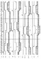
図18Aは、従来の液晶表示装置で中間調を表示するときのタイミングチャートであり、図18Bは、従来の液晶表示装置で黒を表示するときのタイミングチャートである。これらの図面では、Sは階調信号線の電圧、G1〜Gnは走査線の電圧、D1〜Dnは液晶素子に印加される実効電圧、Cs_1〜Cs_nは補助容量線の電圧(各走査線と平行な部分の電圧)を表す。 FIG. 18A is a timing chart when a halftone is displayed on the conventional liquid crystal display device, and FIG. 18B is a timing chart when black is displayed on the conventional liquid crystal display device. In these drawings, S is a voltage of the gradation signal line, G1 to Gn are voltages of the scanning lines, D1 to Dn are effective voltages applied to the liquid crystal elements, and Cs_1 to Cs_n are voltages of the auxiliary capacitance lines (each scanning line and Voltage of the parallel part).
走査線駆動回路91は走査線G1〜Gnに対して順に選択電圧(ハイレベル)を与え、階調信号線駆動回路92は階調信号線S1〜Smに対して映像データに応じた階調電圧を与える。液晶素子95に同じ極性の電圧を印加し続けると、分極が発生し、焼きつきの原因となる。このため、階調信号線駆動回路92は、階調信号線S1〜Smに対して1フレームごとに逆極性の電圧を与える。 The scanning
走査線Giの電圧がハイレベルである間、走査線Giに接続されたTFT94はオン状態となり、階調信号線S1〜Smの電圧は液晶素子95の画素電極に書き込まれる。また、補助容量線Csには一定の電圧が与えられる。このため、走査線Giの電圧がローレベルに変化した後は、画素電極に書き込まれた電圧は走査線Giの電圧が再びハイレベルとなるまで保持され、液晶素子95の輝度は1フレーム期間内では一定となる。 While the voltage of the scanning line Gi is at a high level, the
本願発明に関連して、以下の先行技術が知られている。特許文献1には、液晶表示装置の動画性能を改善するために、各画素の時間軸方向のレベル変動を検出し、検出出力に応じて入力画像信号の各画素の時間軸方向に高域強調フィルタをかけた結果を液晶表示部に出力することが記載されている。特許文献2には、1フレーム期間の実効電圧を上げるために、スイッチング素子のオフ期間に、蓄積容量を介して画素電極に接続された第1の配線に第1の変調信号を印加し、対向電極に第2の変調信号を印加することが記載されている。特許文献3には、1フレーム期間の実効電圧を上げるために、スイッチング素子のオフ期間に、蓄積容量を介して画素電極に接続された第1の配線に1フィールドごとに電圧が逆向きに変化する変調信号を与えることが記載されている。
しかしながら、特許文献1に記載された液晶表示装置には、各画素の時間軸方向のレベル変動を検出するために、前フレームの画像信号を蓄積するメモリが必要となる。このため、回路規模が大きくなり、コストや消費電力も大きくなる。このように特許文献1に記載された液晶表示装置には、小型、薄型、狭額縁などの要求に逆行するという問題がある。また、特許文献2および3に記載された液晶表示装置は、液晶素子に印加される実効電圧を上げることを目的として構成されており、応答速度を改善するための考慮がなされていない。 However, the liquid crystal display device described in
それ故に、本発明は、回路規模を増大させずに応答速度を改善した液晶表示装置を提供することを目的とする。 Therefore, an object of the present invention is to provide a liquid crystal display device having an improved response speed without increasing the circuit scale.
第1の発明は、アクティブマトリクス型の液晶表示装置であって、
複数の走査線と、
複数の階調信号線と、
複数の補助容量線と、
前記走査線と前記階調信号線の交点に対応して配置され、
前記走査線に接続された制御端子を有するスイッチング素子と、
前記スイッチング素子を介して前記階調信号線に接続された画素電極を有する液晶素子と、
前記画素電極と前記補助容量線に接続された補助容量とを含む複数の画素回路と、
前記走査線、前記階調信号線および前記補助容量線を駆動する駆動回路とを備え、
前記駆動回路は、前記スイッチング素子がオフ状態である期間の一部において、前記液晶素子に印加される実効電圧を高くするための特定電圧を前記補助容量線に与えることを特徴とする。The first invention is an active matrix type liquid crystal display device,
A plurality of scan lines;
A plurality of gradation signal lines;
A plurality of auxiliary capacitance lines;
Arranged corresponding to the intersection of the scanning line and the gradation signal line,
A switching element having a control terminal connected to the scanning line;
A liquid crystal element having a pixel electrode connected to the gradation signal line via the switching element;
A plurality of pixel circuits including the pixel electrode and an auxiliary capacitor connected to the auxiliary capacitor line;
A driving circuit for driving the scanning line, the gradation signal line, and the auxiliary capacitance line;
The drive circuit applies a specific voltage to the auxiliary capacitance line for increasing an effective voltage applied to the liquid crystal element during a part of a period in which the switching element is off.
第2の発明は、第1の発明において、
前記駆動回路は、前記補助容量線の電圧を前記特定電圧を含めて2段階に切り替えることを特徴とする。According to a second invention, in the first invention,
The drive circuit switches the voltage of the auxiliary capacitance line in two stages including the specific voltage.
第3の発明は、第1または第2の発明において、
前記駆動回路は、前記スイッチング素子がオン状態に変化する直前に、前記補助容量線に前記特定電圧を与えることを特徴とする。According to a third invention, in the first or second invention,
The drive circuit applies the specific voltage to the storage capacitor line immediately before the switching element changes to an ON state.
第4の発明は、第1または第2の発明において、
前記駆動回路は、前記補助容量線のうち2本以上に同じタイミングで前記特定電圧を与えることを特徴とする。4th invention is 1st or 2nd invention,
The drive circuit applies the specific voltage to two or more of the auxiliary capacitance lines at the same timing.
第5の発明は、第1〜第4のいずれかの発明において、
前記補助容量線の電圧変化に同期して点灯および消灯する複数のバックライトをさらに備える。A fifth invention is any one of the first to fourth inventions,
A plurality of backlights that are turned on and off in synchronization with a voltage change of the auxiliary capacitance line are further provided.
第6の発明は、第1〜第4のいずれかの発明において、
連続的に発光するバックライトと、
前記バックライトの出射光の経路を前記補助容量線の電圧変化に同期して変化させる導光体とをさらに備える。A sixth invention is any one of the first to fourth inventions,
A backlight that emits light continuously;
A light guide that changes a path of light emitted from the backlight in synchronization with a voltage change of the auxiliary capacitance line;
上記第1の発明によれば、液晶素子に印加される実効電圧を1フレーム期間内で変化させることにより、階調表示を正しく行いながら、回路規模を増大させずに応答速度を速くすることができる。 According to the first aspect of the invention, by changing the effective voltage applied to the liquid crystal element within one frame period, the response speed can be increased without increasing the circuit scale while correctly performing gradation display. it can.
上記第2の発明によれば、補助容量線の駆動回路を容易に構成することができる。 According to the second aspect of the invention, the drive circuit for the auxiliary capacitance line can be easily configured.
上記第3の発明によれば、補助容量線の電圧が変化する回数を減らし、液晶表示装置の消費電力を削減することができる。 According to the third aspect, it is possible to reduce the number of times the voltage of the auxiliary capacitance line changes and reduce the power consumption of the liquid crystal display device.
上記第4の発明によれば、補助容量線に接続される入力端子の数を減らし、配線の引き回しによる額縁の増加を防止することができる。 According to the fourth aspect of the invention, the number of input terminals connected to the auxiliary capacitance line can be reduced, and an increase in the frame due to wiring routing can be prevented.
上記第5または第6の発明によれば、液晶素子の透過率が大きくなるときにバックライトを消灯させることにより、黒表示のときの白浮きを防止することができる。また、黒挿入によるインパルス駆動を行うことにより、ホールド型の表示装置で発生する残像を抑え、表示品位を高めることができる。また、上記第6の発明によれば、光源の個数を増やさずにバックライトを構成することができる。 According to the fifth or sixth aspect of the invention, it is possible to prevent white floating during black display by turning off the backlight when the transmittance of the liquid crystal element increases. Further, by performing impulse driving by black insertion, it is possible to suppress an afterimage generated in the hold-type display device and improve display quality. Further, according to the sixth aspect, the backlight can be configured without increasing the number of light sources.
以下、図面を参照して、本発明の各実施形態に係る液晶表示装置について説明する。以下の説明では、nおよびmは2以上の整数、iは1以上n以下の整数、jは1以上m以下の整数であるとする。 Hereinafter, a liquid crystal display device according to each embodiment of the present invention will be described with reference to the drawings. In the following description, n and m are integers of 2 or more, i is an integer of 1 to n, and j is an integer of 1 to m.
(第1の実施形態)
図1は、本発明の第1の実施形態に係る液晶表示装置の構成を示す図である。図1に示す液晶表示装置1は、n本の走査線G1〜Gn、m本の階調信号線S1〜Sm、n本の補助容量線Cs1〜Csn、(m×n)個の画素回路Aij、走査線駆動回路11、階調信号線駆動回路12、および、補助容量線駆動回路13を備えたアクティブマトリクス型の液晶表示装置である。液晶表示装置1は、ノーマリーブラック型であるとする。(First embodiment)
FIG. 1 is a diagram showing a configuration of a liquid crystal display device according to the first embodiment of the present invention. The liquid
図1に示すように、走査線G1〜Gnは互いに平行に配置され、階調信号線S1〜Smは走査線G1〜Gnと直交するように互いに平行に配置される。画素回路Aijは、走査線G1〜Gnと階調信号線S1〜Smの交点に対応してマトリクス状に配置される。補助容量線Cs1〜Csnは、画素回路Aijの各行に対応して設けられ、走査線G1〜Gnと平行に配置される。 As shown in FIG. 1, the scanning lines G1 to Gn are arranged in parallel to each other, and the gradation signal lines S1 to Sm are arranged in parallel to each other so as to be orthogonal to the scanning lines G1 to Gn. The pixel circuits Aij are arranged in a matrix corresponding to the intersections of the scanning lines G1 to Gn and the gradation signal lines S1 to Sm. The auxiliary capacitance lines Cs1 to Csn are provided corresponding to each row of the pixel circuit Aij, and are arranged in parallel with the scanning lines G1 to Gn.
図2は、画素回路Aijの等価回路図である。図2に示すように、画素回路Aijは、スイッチング素子であるTFT21、液晶素子(液晶容量)22、および、補助容量23を含んでいる。TFT21のゲート端子は走査線Giに接続され、ソース端子は階調信号線Sjに接続され、ドレイン端子は画素電極Pijに接続される。液晶素子22は、画素回路ごとに設けられる画素電極Pijとすべての画素回路に共通する対向電極Vcomとの間に液晶材料を挟み込むことにより形成される。補助容量23は、画素電極Pijと補助容量線Csiとの間に絶縁膜を挟み込むことにより形成される。 FIG. 2 is an equivalent circuit diagram of the pixel circuit Aij. As illustrated in FIG. 2, the pixel circuit Aij includes a
走査線駆動回路11と階調信号線駆動回路12は、従来の液晶表示装置と同様に、走査線G1〜Gnと階調信号線S1〜Smを駆動する。走査線駆動回路11は、走査線G1〜Gnの中から1本の走査線を順に選択し、選択した走査線に選択電圧(ハイレベル)を与え、それ以外の走査線には非選択電圧(ローレベル)を与える。階調信号線駆動回路12は、映像データに応じた階調電圧を階調信号線S1〜Smに与える。階調信号線駆動回路12は、焼きつきを防止するために、対向電極Vcomの電圧よりも高い電圧(正の階調電圧)と、対向電極Vcomの電圧よりも低い電圧(負の階調電圧)とを1フレームごとに切り替えて階調信号線S1〜Smに与える。 The scanning
画素回路Aij内のTFT21は、走査線Giの選択期間ではオン状態、それ以外のときにはオフ状態となる。走査線Giの選択期間では、階調信号線駆動回路12は画素電極Pijに書き込むべき階調電圧を階調信号線Sjに与え、画素電極Pijの電圧は与えられた階調電圧に等しくなる。走査線Giの選択期間が終了すると、画素回路Aij内のTFT21はオフ状態に変化する。これ以降、画素電極Pijは階調信号線Sjから電気的に切り離され、画素電極Pijの電圧は階調信号線Sjの電圧の変化の影響を受けなくなる。液晶素子22には画素電極Pijと対向電極Vcomの電位差(以下、実効電圧という)が印加され、液晶素子22の透過率は実効電圧に応じて変化する。このようにして、液晶表示装置1は階調表示を行う。 The
補助容量線駆動回路13は、補助容量線Cs1〜Csnを個別に駆動する。補助容量線駆動回路13は、補助容量線Cs1〜Csnに対して、画素回路Aij内のTFT21がオフ状態である期間の一部(以下、走査線Giに係る特定期間という)において、画素回路Aij内の液晶素子22に印加される実効電圧を高くするための電圧(以下、特定電圧という)を与える。補助容量線駆動回路13の作用により、補助容量線Csiの電圧は1フレーム期間内で変化する。 The auxiliary capacitance
補助容量線Csiの電圧が変化したときに、画素回路Aij内の液晶素子22に印加される実効電圧は以下のように変化する。なお、実効電圧の変化を厳密に評価するときには、走査線G1〜Gmと画素電極Pijの間の寄生容量Cgdなどを考慮する必要があるが、ここでは理解を容易にするため、Cgdなど他の寄生容量を無視するものとする。 When the voltage of the storage capacitor line Csi changes, the effective voltage applied to the
液晶素子22の容量値をClc、補助容量23の容量値をCs、対向電極Vcomの電圧をVc(固定値)、TFT21がオン状態のときに画素電極Pijに書き込まれた電圧をVoとする。TFT21がオフ状態である間に、補助容量線Csiの電圧がVaからVbに変化し、これに伴い、画素電極Pijの電圧がVoからVxに変化したとする。TFT21がオフ状態である間、画素電極Pijに蓄積された電荷の量は変化しないので、次式(1)が成立する。
Cs(Vo−Va)+Clc(Vo−Vc)
=Cs(Vx−Vb)+Clc(Vx−Vc) …(1)
したがって、ΔVcs=Vb−Va、ΔVpix=Vx−Voとおくと、次式(2)が得られる。
ΔVpix=Cs/(Cs+Clc)×ΔVcs …(2)The capacitance value of the
Cs (Vo-Va) + Clc (Vo-Vc)
= Cs (Vx-Vb) + Clc (Vx-Vc) (1)
Therefore, when ΔVcs = Vb−Va and ΔVpix = Vx−Vo, the following equation (2) is obtained.
ΔVpix = Cs / (Cs + Clc) × ΔVcs (2)
このように、実効電圧の変化量ΔVpixは、補助容量線の電圧振幅ΔVcsに比例する。例えば、液晶素子22と補助容量23の容量値の比が1:1で、画素電極Pijに書き込まれた電圧Voが+3Vであるときに、補助容量線の電圧を4V高くすると、画素電極Pijの電圧は2V高くなり+5Vとなる。なお、ここでは対向電極Vcomの電圧は固定値であるとしたが、実効電圧の極性に応じて対向電極Vcomの電圧を変化させる場合にも、同様の結果が得られる。 Thus, the change amount ΔVpix of the effective voltage is proportional to the voltage amplitude ΔVcs of the auxiliary capacitance line. For example, when the ratio of the capacitance values of the
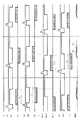
図3は、液晶表示装置1で中間調を表示するときのタイミングチャートである。図3および以降のタイミングチャートでは、Sは階調信号線の電圧、G1〜Gnは走査線の電圧、D1〜Dnは液晶素子に印加される実効電圧、Cs1〜Csnは補助容量線の電圧、T1〜Tnは特定期間を表す。液晶表示装置1は、実効電圧の極性をラインごとおよびフレームごとに反転させるライン反転駆動を行う。 FIG. 3 is a timing chart when the halftone is displayed on the liquid
図3に示すように、走査線Giの電圧は、1フレーム期間の1ライン時間(走査線Giの選択期間)ではハイレベル、それ以外ではローレベルとなる。走査線Giの選択期間では、階調信号線Sに正の階調電圧が与えられるときと、負の階調電圧が与えられるときとがある。いずれの場合も、画素回路Aij内の液晶素子22に印加される実効電圧Diは、与えられた階調電圧と対向電極Vcomの電圧との差となる。走査線Giの選択期間が終了するときに、実効電圧Diは引き込み分だけ低下する。 As shown in FIG. 3, the voltage of the scanning line Gi is at a high level during one line time (selection period of the scanning line Gi) of one frame period, and is at a low level otherwise. In the selection period of the scanning line Gi, there are a case where a positive gradation voltage is applied to the gradation signal line S and a case where a negative gradation voltage is applied. In any case, the effective voltage Di applied to the
図3に示す例では、走査線Giに係る特定期間は、走査線Giの選択期間が終了して1ライン時間後に始まる。補助容量線駆動回路13は、走査線Giの選択期間で正の階調電圧が与えられたときには、それに続く走査線Giの非選択期間(特定期間を除く)では電圧V2を補助容量線Cs1〜Csnに与え、走査線Giに係る特定期間では電圧V2よりも高い電圧V1(V1>V2)を補助容量線Cs1〜Csnに与える。また、補助容量線駆動回路13は、走査線Giの選択期間で負の階調電圧が与えられたときには、それに続く走査線Giの非選択期間(特定期間を除く)では電圧V2を補助容量線Cs1〜Csnに与え、走査線Giに係る特定期間では電圧V1を補助容量線Cs1〜Csnに与える。 In the example shown in FIG. 3, the specific period related to the scanning line Gi starts one line time after the selection period of the scanning line Gi ends. When a positive gradation voltage is applied in the selection period of the scanning line Gi, the auxiliary capacitance
例えば図3に示す特定期間T1における補助容量線Cs1の電圧は、その前の選択期間で正の階調電圧が与えられたことに対応して、特定期間T1の前後よりも高くなる。一方、図3に示す特定期間T1’における補助容量線Cs1の電圧は、その前の選択期間で負の階調電圧が与えられたことに対応して、特定期間T1’の前後よりも低くなる。以下、特定期間の前後よりも高い特定電圧を正の特定電圧、特定期間の前後よりも低い特定電圧を負の特定電圧という。 For example, the voltage of the auxiliary capacitance line Cs1 in the specific period T1 shown in FIG. 3 becomes higher than before and after the specific period T1 in response to the positive gradation voltage being given in the previous selection period. On the other hand, the voltage of the storage capacitor line Cs1 in the specific period T1 ′ shown in FIG. 3 becomes lower than before and after the specific period T1 ′ in response to the negative gradation voltage being applied in the previous selection period. . Hereinafter, the specific voltage higher than before and after the specific period is referred to as a positive specific voltage, and the specific voltage lower than before and after the specific period is referred to as a negative specific voltage.
上述したように、実効電圧の変化量は、補助容量線の電圧振幅に比例する。したがって、上記のように補助容量線Cs1〜Csnの電圧を特定電圧を含めて2段階に切り替えることにより、実効電圧の極性にかかわらず、特定期間における実効電圧をそれ以外のときよりも高くすることができる。 As described above, the change amount of the effective voltage is proportional to the voltage amplitude of the auxiliary capacitance line. Therefore, by switching the voltage of the auxiliary capacitance lines Cs1 to Csn into two stages including the specific voltage as described above, the effective voltage in the specific period is made higher than in other cases regardless of the polarity of the effective voltage. Can do.
以下、図4を参照して、本実施形態に係る液晶表示装置1の効果を説明する。図4は、液晶表示装置1と従来の液晶表示装置の応答波形を示す図である。図4には、液晶表示装置1で黒の後に中間調を表示するときの応答波形(太実線)と、従来の液晶表示装置で黒の後に中間調を表示するときの応答波形(太破線)と、従来の液晶表示装置で黒の後に白を表示するときの応答波形(細破線)とが記載されている。 Hereinafter, the effects of the liquid
液晶素子の透過率は、液晶素子に印加される実効電圧の変化に伴って変化する。しかし、液晶素子を構成する液晶材料は粘性を有するので、液晶素子の透過率は実効電圧の変化よりもある程度遅れて変化する。一般に、液晶素子の応答速度は、実効電圧が高いほど速くなる。例えばノーマリーブラック型の液晶表示装置では、階調が低いときほど、実効電圧は低くなり、応答速度は遅くなる。このため、従来の液晶表示装置では、図4に示すように、白表示のときの応答速度は1フレーム期間よりも短いが、中間調表示のときの応答速度は1フレーム期間よりも長くなることがある。このように従来のノーマリーブラック型の液晶表示装置では、低階調(黒に近い階調)を表示するときの応答速度が遅いことが問題となる。 The transmittance of the liquid crystal element changes as the effective voltage applied to the liquid crystal element changes. However, since the liquid crystal material constituting the liquid crystal element has viscosity, the transmittance of the liquid crystal element changes with a certain delay from the change in effective voltage. In general, the response speed of the liquid crystal element increases as the effective voltage increases. For example, in a normally black liquid crystal display device, the lower the gradation, the lower the effective voltage and the slower the response speed. Therefore, in the conventional liquid crystal display device, as shown in FIG. 4, the response speed for white display is shorter than one frame period, but the response speed for halftone display is longer than one frame period. There is. As described above, the conventional normally black liquid crystal display device has a problem in that the response speed when displaying a low gradation (gradation close to black) is slow.
この問題を解決するために、液晶表示装置1は、走査線G1〜Gnに係る特定期間では補助容量線Cs1〜Csnに特定電圧を与える補助容量線駆動回路13を備えている。このため、画素回路Aij内の液晶素子22の透過率は、走査線Giに係る特定期間ではそれ以外のときよりも速く変化する。したがって、液晶表示装置1が黒の後に中間調を表示するときには、液晶素子22の透過率は、特定期間では白表示のときと同様に高速に変化し、従来の液晶表示装置よりも短時間で最終値(映像データに応じた値)に到達する。 In order to solve this problem, the liquid
また、1フレーム期間内に実効電圧が高い期間と低い期間がある場合、液晶素子の表示階調(視覚的階調)は、両期間における階調を両期間の長さで加重平均した階調となる。このため、液晶表示装置1では、特定電圧のレベルを好適に設定することにより、階調表示を正しく行うことができる。さらに液晶表示装置1は、特許文献1に記載された液晶表示装置とは異なり、前フレームの画像信号を蓄積するメモリを備えていない。 In addition, when there are a high effective voltage period and a low effective voltage period within one frame period, the display gradation (visual gradation) of the liquid crystal element is a gradation obtained by weighted averaging of gradations in both periods over the length of both periods. It becomes. Therefore, in the liquid
以上に示すように、本実施形態に係る液晶表示装置1によれば、補助容量線駆動回路13を用いて液晶素子22に印加される実効電圧を1フレーム期間内で変化させることにより、階調表示を正しく行いながら、回路規模を増大させずに応答速度(特に、低階調を表示するときの応答速度)を速くすることができる。 As described above, according to the liquid
また、補助容量線駆動回路13は補助容量線Cs1〜Csnの電圧を特定電圧を含めて2段階に切り替えるので、補助容量線駆動回路13を容易に構成することができる。なお、補助容量線駆動回路13は、例えば図5〜図7に示すように補助容量線Cs1〜Csnの電圧を制御してもよい。これにより、以下の液晶表示装置を構成することができる。 Further, since the storage capacitor
第1の変形例に係る液晶表示装置(図5)では、補助容量線駆動回路13は、補助容量線Cs1〜Csnの電圧を特定電圧を含めて3段階に切り替える。より詳細には、補助容量線駆動回路13は、補助容量線Cs1〜Csnに対して、特定期間以外では電圧V0を与え、正の階調電圧が与えられた後の特定期間では電圧V0よりも高い電圧V1(V1>V0)を与え、負の階調電圧が与えられた後の特定期間では電圧V0よりも低い電圧V2(V2<V0)を与える。これにより、図3に示す場合と同様に、実効電圧の極性にかかわらず、特定期間における実効電圧をそれ以外のときよりも高くすることができる。 In the liquid crystal display device according to the first modification (FIG. 5), the storage capacitor
第2の変形例に係る液晶表示装置(図6)では、走査線Giに係る特定期間は、走査線Giの選択期間の直前に設けられる。補助容量線駆動回路13は、画素回路Aij内のTFT21がオン状態に変化する直前に補助容量線Csiに特定電圧を与える。これにより、補助容量線Cs1〜Csnの電圧が変化する回数を減らし、液晶表示装置の消費電力を削減することができる。 In the liquid crystal display device (FIG. 6) according to the second modification, the specific period related to the scanning line Gi is provided immediately before the selection period of the scanning line Gi. The auxiliary capacitance
第3の変形例に係る液晶表示装置(図7)では、補助容量線駆動回路13は、補助容量線Cs1〜Csnのうち2本以上に同じタイミングで特定電圧を与える。図7に示す例では、走査線G1〜Gnに係る特定期間は、いずれも走査線Gnの選択期間が終了して1ライン時間後に始まる。補助容量線駆動回路13は、特定期間では、奇数番目の補助容量線にはある極性の特定電圧を与え、偶数番目の補助容量線には逆極性の特定電圧を与える。このように補助容量線Cs1〜Csnの半分ずつに同じタイミングで特定電圧を与えることにより、ライン反転駆動を正しく行いながら、補助容量線Cs1〜Csnに接続される入力端子の数を減らし、配線の引き回しによる額縁の増加を防止することができる。また、補助容量線駆動回路13は、補助容量線Cs1〜Csnを複数のグループに分割し、グループ内の補助容量線の半分ずつに同じタイミングで異なる極性の特定電圧を与えてもよい。この場合も同様の効果が得られる。 In the liquid crystal display device according to the third modification (FIG. 7), the auxiliary capacitance
以下、第1の実施形態およびその変形例に係る液晶表示装置で発生することがある白浮きについて説明する。これらの液晶表示装置の応答速度と表示階調は、特定期間の長さや実効電圧の変化量ΔVpixに依存する。図8A〜図8Cに、表示階調を同じにして、実効電圧の変化量ΔVpixをゼロ、小、大に切り替えた場合の輝度の変化を示す。このように、実効電圧の変化量ΔVpixが大きいほど、輝度は高速に変化し、応答速度は速くなる。このことから、応答速度を速くするためには、実効電圧の変化量ΔVpixが大きい(補助容量線Cs1〜Csnの電圧振幅ΔVcsが大きい)ことが好ましいと言える。 Hereinafter, whitening that may occur in the liquid crystal display device according to the first embodiment and the modification thereof will be described. The response speed and display gradation of these liquid crystal display devices depend on the length of the specific period and the change amount ΔVpix of the effective voltage. 8A to 8C show changes in luminance when the display gradation is the same and the change amount ΔVpix of the effective voltage is switched between zero, small, and large. As described above, the larger the change amount ΔVpix of the effective voltage, the faster the luminance changes and the faster the response speed. From this, it can be said that in order to increase the response speed, it is preferable that the change amount ΔVpix of the effective voltage is large (the voltage amplitude ΔVcs of the auxiliary capacitance lines Cs1 to Csn is large).
ところが、補助容量線Cs1〜Csnの電圧は、表示階調にかかわらず同じように変化する。このため、補助容量線Cs1〜Csnの電圧振幅ΔVcsを大きくすると、画素電極Pijに書き込まれた階調電圧Voがゼロでも、補助容量線Cs1〜Csnの電圧が変化しただけで液晶の配向が変化し、液晶素子22の透過率が変化することがある。図9は、黒表示のときに白浮きが発生する様子を示すタイミングチャートである。図9では、階調信号線Sにゼロの階調電圧を与えたにもかかわらず、補助容量線Csiに特定期間で特定電圧を与えたために、特定期間の終端付近では輝度が非ゼロとなっている。 However, the voltages of the auxiliary capacitance lines Cs1 to Csn change in the same manner regardless of the display gradation. For this reason, when the voltage amplitude ΔVcs of the auxiliary capacitance lines Cs1 to Csn is increased, even if the gradation voltage Vo written to the pixel electrode Pij is zero, the orientation of the liquid crystal changes only by changing the voltage of the auxiliary capacitance lines Cs1 to Csn. In addition, the transmittance of the
このため、ノーマリーブラック型の液晶表示装置では、黒を表示するときに、バックライトの光を十分に遮断できず、表示画面が完全に黒くならないことがある(この現象を白浮きという)。そこで、第2および第3の実施形態では、白浮きを防止した液晶表示装置について説明する。なお、補助容量線Csiに特定期間で特定電圧を与えても白浮きが問題にならない液晶表示装置については、以下の対策を施すことは必ずしも必要ではない。 For this reason, in the normally black type liquid crystal display device, when displaying black, the light of the backlight cannot be sufficiently blocked, and the display screen may not be completely black (this phenomenon is called whitening). In the second and third embodiments, a liquid crystal display device that prevents whitening will be described. Note that it is not always necessary to take the following measures for a liquid crystal display device in which whitening does not become a problem even when a specific voltage is applied to the storage capacitor line Csi for a specific period.
(第2の実施形態)
第2の実施形態に係る液晶表示装置は、第1の実施形態に係る液晶表示装置1と同じ構成を有する(図1を参照)。図10は、本実施形態に係る液晶表示装置で中間調を表示するときのタイミングチャートである。補助容量線駆動回路13は、図10に示すように、走査線Giの選択期間で正の階調電圧が与えられたときには、それに続く走査線Giの非選択期間(特定期間を除く)では電圧V1を補助容量線Cs1〜Csnに与え、走査線Giに係る特定期間では電圧V1よりも低い電圧V2(V2<V1)を補助容量線Cs1〜Csnに与える。また、補助容量線駆動回路13は、走査線Giの選択期間で負の階調電圧が与えられたときには、それに続く走査線Giの非選択期間(特定期間を除く)では電圧V2を補助容量線Cs1〜Csnに与え、走査線Giに係る特定期間では電圧V1を補助容量線Cs1〜Csnに与える。(Second Embodiment)
The liquid crystal display device according to the second embodiment has the same configuration as the liquid
上述したように、第1の実施形態に係る補助容量線駆動回路13は、特定期間では、選択期間で正の階調電圧が与えられたときには正の特定電圧を与え、選択期間で負の階調電圧が与えられたときには負の特定電圧を与える。これに対して、本実施形態に係る補助容量線駆動回路13は、特定期間では、選択期間で正の階調電圧が与えられたときには負の特定電圧を与え、選択期間で負の階調電圧が与えられたときには正の特定電圧を与える。この補助容量線駆動回路13を用いても、特定期間で液晶素子22に印加される実効電圧を高くすることにより、回路規模を増大させずに応答速度を速くすることができる。 As described above, the storage capacitor
図11は、液晶の応答特性を示す図である。図11に示すように、液晶素子の透過率は、実効電圧が高くなるに従って高くなるが、実効電圧が閾値電圧Vth以下のときには最小値Xでほぼ一定となる。そこで、この特性を利用し、電圧V1、V2を決定するときには、白浮きが問題とならない範囲内で、両者の差ΔVcsが最大となる電圧を選択すればよい。 FIG. 11 is a diagram showing the response characteristics of the liquid crystal. As shown in FIG. 11, the transmittance of the liquid crystal element increases as the effective voltage increases. However, when the effective voltage is equal to or lower than the threshold voltage Vth, the transmittance is almost constant at the minimum value X. Therefore, when determining the voltages V1 and V2 using this characteristic, a voltage that maximizes the difference ΔVcs between the two may be selected within a range where whitening does not become a problem.
以上に示すように、本実施形態に係る液晶表示装置によれば、第1の実施形態に係る液晶表示装置よりも補助容量線Csiの電圧振幅ΔVcsを大きくし、応答速度をより速くすると共に、黒表示のときの白浮きを防止することができる。 As described above, according to the liquid crystal display device according to the present embodiment, the voltage amplitude ΔVcs of the auxiliary capacitance line Csi is increased and the response speed is made faster than in the liquid crystal display device according to the first embodiment. White floating during black display can be prevented.
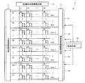
(第3の実施形態)
図12は、本発明の第3の実施形態に係る液晶表示装置の構成を示す図である。図12に示す液晶表示装置3は、第1の実施形態に係る液晶表示装置1に、4個のバックライト31〜34とバックライト制御回路35を追加したものである。本実施形態の構成要素のうち第1の実施形態と同一の要素については、同一の参照符号を付して説明を省略する。(Third embodiment)
FIG. 12 is a diagram showing a configuration of a liquid crystal display device according to the third embodiment of the present invention. A liquid crystal display device 3 shown in FIG. 12 is obtained by adding four
液晶表示装置3では、(m×n)個の画素回路は、走査線方向に4つのブロックに分割される。以下、4つのブロックを上から順に第1〜第4ブロックといい、a=n/4、b=n/2、c=3n/4とする。バックライト31〜34は、それぞれ、第1〜第4ブロックに対応して設けられる。 In the liquid crystal display device 3, (m × n) pixel circuits are divided into four blocks in the scanning line direction. Hereinafter, the four blocks are referred to as the first to fourth blocks in order from the top, and a = n / 4, b = n / 2, and c = 3n / 4. The
バックライト31〜34は、バックライト制御回路35からの制御に従い、補助容量線Cs1〜Csnの電圧変化に同期して点灯および消灯する。図13は、1フレーム期間内のバックライト31〜34の状態を示す図である。液晶表示装置3では、1フレーム期間は4つの期間に分割され、各期間ではバックライト31〜34のうち3個が点灯し、残りの1個は消灯する。最初の期間ではバックライト31が消灯し、次の期間ではバックライト32が消灯し、その次の期間ではバックライト33が消灯し、最後の期間ではバックライト34が消灯する。なお、図13において、A1〜A4は、補助容量線に特定電圧が与えられている範囲を表す。 The
走査線駆動回路11と階調信号線駆動回路12は、従来の液晶表示装置と同様に、走査線G1〜Gnと階調信号線S1〜Smを駆動する。補助容量線駆動回路13は、補助容量線Cs1〜Csnを4つのグループに分割し、グループ内の補助容量線の半分ずつに同じタイミングで異なる極性の特定電圧を与える。 The scanning
図14は、液晶表示装置3で中間調を表示するときのタイミングチャートであり、図15は、液晶表示装置3で黒を表示するときのタイミングチャートである。これらの図面で点状模様を付した部分は、バックライトが消灯している期間を表す。 FIG. 14 is a timing chart when halftone is displayed on the liquid crystal display device 3, and FIG. 15 is a timing chart when black is displayed on the liquid crystal display device 3. In these drawings, a portion with a dotted pattern represents a period during which the backlight is turned off.
第1ブロックには、走査線G1〜Gaと補助容量線Cs1〜Csaが配置されている。走査線G1〜Gaに係る特定期間は、いずれも走査線Gaの選択期間が終了して1ライン時間後に始まる。補助容量線駆動回路13は、ある特定期間では補助容量線Cs1〜Csaのうち奇数番目の補助容量線には正の特定電圧を与えると同時に、偶数番目の補助容量線には負の特定電圧を与え、次の特定期間では補助容量線Cs1〜Csaに前回とは逆極性の特定電圧を与える。 In the first block, scanning lines G1 to Ga and storage capacitor lines Cs1 to Csa are arranged. Each of the specific periods related to the scanning lines G1 to Ga starts one line time after the selection period of the scanning line Ga ends. The auxiliary capacitance
第1ブロック内の画素回路に含まれる液晶素子の透過率は、走査線G1〜Gaに係る特定期間の終端付近で最大となる。これに合わせて、バックライト31は、走査線G1〜Gaに係る特定期間の終端を含む所定期間で消灯する。バックライト31が消灯している間、第1ブロック内の画素回路に含まれる液晶素子の輝度はゼロとなる。 The transmittance of the liquid crystal element included in the pixel circuit in the first block is maximized near the end of the specific period related to the scanning lines G1 to Ga. In accordance with this, the
補助容量線駆動回路13は、第1ブロックに配置された補助容量線Cs1〜Csaと同様に、第2ブロックに配置された補助容量線Csa+1〜Csb、第3ブロックに配置された補助容量線Csb+1〜Csc、および、第4ブロックに配置された補助容量線Csc+1〜Csnを駆動する。バックライト32は、走査線Ga+1〜Gbに係る特定期間の終端を含む所定期間で消灯する。バックライト33、34もこれと同様である。バックライト32〜34が消灯している間、第2〜第4ブロック内の画素回路に含まれる液晶素子の輝度はゼロとなる。 The auxiliary capacitance
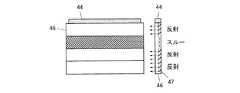
図16A〜図16Dは、バックライト31〜34の構成例を示す図である。これらの図面では、点状模様と無模様はその部材が明るいことを表し、クロスハッチと黒塗りはその部材が暗いことを表す。バックライト31〜34は、例えば、マトリクス状に配置された直下型LED(Light Emitting Diode)バックライト41と、行間では光が伝搬しない4行構成の導光板45とを用いて構成される(図16A)。この場合、直下型LEDバックライト41は、行単位で点灯および消灯する。あるいは、直下型LEDバックライト41に代えて、直下型CCFL(Cold Cathode Fluorescent Lamp )バックライト42を用いてもよい(図16B)。あるいは、これらの直下型バックライトに代えて、エッジ型LEDバックライト43を用いてもよい(図16C)。あるいは、LEDやCCFLに代えて、EL(Electro Luminescence:エレクトロルミネッセンス)などを用いてもよい。導光板45は、PMMA(Polymethylmethacrylate:メタクリル酸メチル)、PC(Polycarbonate :ポリカーボネート)などの樹脂や液晶材料やガラスなどで構成される。 16A to 16D are diagrams illustrating configuration examples of the
あるいは、バックライト31〜34を、LEDやCCFLなどのエッジ型バックライト44と、反射板47を内蔵した導光体46とを用いて構成してもよい(図16D)。この場合、エッジ型バックライト44は連続的に点灯する。導光体46は、液晶フィルタやメタルなどで形成された反射板47を用いて、エッジ型バックライト44の出射光の経路を補助容量線Cs1〜Csnの電圧変化に同期して変化させる。これにより、光源の個数を増やさずにバックライト31〜34を構成することができる。 Or you may comprise the backlights 31-34 using the
以上に示すように、本実施形態に係る液晶表示装置3では、液晶素子22の透過率が大きくなるときには、バックライト31〜34が消灯し、液晶素子22の輝度はゼロとなる。したがって、液晶表示装置3によれば、第1の実施形態に係る液晶表示装置1の効果(回路規模を増大させずに応答速度を速くする)に加えて、黒表示のときの白浮きを防止することができる。 As described above, in the liquid crystal display device 3 according to this embodiment, when the transmittance of the
また、液晶表示装置3では、バックライト31〜34が1フレーム期間に1回ずつ消灯する。したがって、液晶表示装置3によれば、黒挿入によってブラウン管と同様のインパルス駆動を行うことにより、ホールド型の表示装置で発生する残像を抑え、表示品位を高めることができる。 In the liquid crystal display device 3, the
なお、以上の説明では、画素回路や補助容量線を4つに分割することとしたが、画素回路や補助容量線の分割数は任意でよい。また、画素回路や補助容量線を分割せずに、垂直帰線期間内でバックライトを消灯させてもよい。また、図14および図15では、各ブロックに対応した特定期間は重ならず、バックライト31〜34の消灯期間も重ならないこととしたが、各ブロックに対応した特定期間は重なってもよく、バックライト31〜34の消灯期間も重なってもよい。 In the above description, the pixel circuit and the auxiliary capacitance line are divided into four. However, the number of divisions of the pixel circuit and the auxiliary capacitance line may be arbitrary. Further, the backlight may be turned off within the vertical blanking period without dividing the pixel circuit and the auxiliary capacitance line. 14 and 15, the specific periods corresponding to the blocks do not overlap and the
1、3…液晶表示装置
11…走査線駆動回路
12…階調信号線駆動回路
13…補助容量線駆動回路
21…TFT
22…液晶素子(液晶容量)
23…補助容量
31〜34…バックライト
35…バックライト制御回路
41…直下型LEDバックライト
42…直下型CCFLバックライト
43…エッジ型LEDバックライト
44…エッジ型バックライト
45…導光板
46…導光体
47…反射板
G1〜Gn…走査線
S1〜Sm…階調信号線
Cs1〜Csn…補助容量線
Aij…画素回路
Pij…画素電極
Vcom…共通電極DESCRIPTION OF
22 ... Liquid crystal element (liquid crystal capacity)
DESCRIPTION OF
Claims (6)
Translated fromJapanese複数の走査線と、
複数の階調信号線と、
複数の補助容量線と、
前記走査線と前記階調信号線の交点に対応して配置され、
前記走査線に接続された制御端子を有するスイッチング素子と、
前記スイッチング素子を介して前記階調信号線に接続された画素電極を有する液晶素子と、
前記画素電極と前記補助容量線に接続された補助容量とを含む複数の画素回路と、
前記走査線、前記階調信号線および前記補助容量線を駆動する駆動回路とを備え、
前記駆動回路は、前記スイッチング素子がオフ状態である期間の一部において、前記液晶素子に印加される実効電圧を高くするための特定電圧を前記補助容量線に与えることを特徴とする、液晶表示装置。An active matrix type liquid crystal display device,
A plurality of scan lines;
A plurality of gradation signal lines;
A plurality of auxiliary capacitance lines;
Arranged corresponding to the intersection of the scanning line and the gradation signal line,
A switching element having a control terminal connected to the scanning line;
A liquid crystal element having a pixel electrode connected to the gradation signal line via the switching element;
A plurality of pixel circuits including the pixel electrode and an auxiliary capacitor connected to the auxiliary capacitor line;
A driving circuit for driving the scanning line, the gradation signal line, and the auxiliary capacitance line;
The liquid crystal display, wherein the driving circuit applies a specific voltage to the auxiliary capacitance line for increasing an effective voltage applied to the liquid crystal element during a part of a period in which the switching element is in an off state. apparatus.
前記バックライトの出射光の経路を前記補助容量線の電圧変化に同期して変化させる導光体とをさらに備えた、請求項1〜4のいずれかに記載の液晶表示装置。A continuously lit backlight,
The liquid crystal display device according to claim 1, further comprising: a light guide that changes a path of light emitted from the backlight in synchronization with a change in voltage of the auxiliary capacitance line.
Priority Applications (1)
| Application Number | Priority Date | Filing Date | Title |
|---|---|---|---|
| JP2007170665AJP2009008919A (en) | 2007-06-28 | 2007-06-28 | Liquid crystal display |
Applications Claiming Priority (1)
| Application Number | Priority Date | Filing Date | Title |
|---|---|---|---|
| JP2007170665AJP2009008919A (en) | 2007-06-28 | 2007-06-28 | Liquid crystal display |
Publications (1)
| Publication Number | Publication Date |
|---|---|
| JP2009008919Atrue JP2009008919A (en) | 2009-01-15 |
Family
ID=40324051
Family Applications (1)
| Application Number | Title | Priority Date | Filing Date |
|---|---|---|---|
| JP2007170665APendingJP2009008919A (en) | 2007-06-28 | 2007-06-28 | Liquid crystal display |
Country Status (1)
| Country | Link |
|---|---|
| JP (1) | JP2009008919A (en) |
Cited By (6)
| Publication number | Priority date | Publication date | Assignee | Title |
|---|---|---|---|---|
| JP2009086620A (en)* | 2007-09-28 | 2009-04-23 | Samsung Electronics Co Ltd | Liquid crystal display device and driving method thereof |
| WO2011001721A1 (en)* | 2009-07-01 | 2011-01-06 | シャープ株式会社 | Image display device |
| WO2011070838A1 (en)* | 2009-12-11 | 2011-06-16 | シャープ株式会社 | Display panel, liquid crystal display, and driving method |
| WO2011070836A1 (en)* | 2009-12-11 | 2011-06-16 | シャープ株式会社 | Display panel, liquid crystal display, and driving method |
| JP2011128272A (en)* | 2009-12-16 | 2011-06-30 | Seiko Epson Corp | Electrophoretic display device, driving method of electrophoretic display device, and electronic device |
| WO2012169160A1 (en)* | 2011-06-07 | 2012-12-13 | シャープ株式会社 | Liquid crystal display device and drive circuit for liquid crystal display device |
Citations (6)
| Publication number | Priority date | Publication date | Assignee | Title |
|---|---|---|---|---|
| JPH10239662A (en)* | 1997-03-03 | 1998-09-11 | Toshiba Corp | Liquid crystal display |
| JP2001265287A (en)* | 2000-03-15 | 2001-09-28 | Sharp Corp | Active matrix display device and driving method thereof |
| JP2002049037A (en)* | 2000-08-03 | 2002-02-15 | Hitachi Ltd | Illumination device and liquid crystal display device using the same |
| JP2002202491A (en)* | 2000-10-25 | 2002-07-19 | Matsushita Electric Ind Co Ltd | Driving method of liquid crystal display device and liquid crystal display device |
| JP2003228345A (en)* | 2002-02-06 | 2003-08-15 | Matsushita Electric Ind Co Ltd | Liquid crystal display |
| JP2005208600A (en)* | 2003-12-26 | 2005-08-04 | Nec Corp | Liquid crystal display device, driving method and driving circuit thereof |
- 2007
- 2007-06-28JPJP2007170665Apatent/JP2009008919A/enactivePending
Patent Citations (6)
| Publication number | Priority date | Publication date | Assignee | Title |
|---|---|---|---|---|
| JPH10239662A (en)* | 1997-03-03 | 1998-09-11 | Toshiba Corp | Liquid crystal display |
| JP2001265287A (en)* | 2000-03-15 | 2001-09-28 | Sharp Corp | Active matrix display device and driving method thereof |
| JP2002049037A (en)* | 2000-08-03 | 2002-02-15 | Hitachi Ltd | Illumination device and liquid crystal display device using the same |
| JP2002202491A (en)* | 2000-10-25 | 2002-07-19 | Matsushita Electric Ind Co Ltd | Driving method of liquid crystal display device and liquid crystal display device |
| JP2003228345A (en)* | 2002-02-06 | 2003-08-15 | Matsushita Electric Ind Co Ltd | Liquid crystal display |
| JP2005208600A (en)* | 2003-12-26 | 2005-08-04 | Nec Corp | Liquid crystal display device, driving method and driving circuit thereof |
Cited By (10)
| Publication number | Priority date | Publication date | Assignee | Title |
|---|---|---|---|---|
| JP2009086620A (en)* | 2007-09-28 | 2009-04-23 | Samsung Electronics Co Ltd | Liquid crystal display device and driving method thereof |
| WO2011001721A1 (en)* | 2009-07-01 | 2011-01-06 | シャープ株式会社 | Image display device |
| WO2011070838A1 (en)* | 2009-12-11 | 2011-06-16 | シャープ株式会社 | Display panel, liquid crystal display, and driving method |
| WO2011070836A1 (en)* | 2009-12-11 | 2011-06-16 | シャープ株式会社 | Display panel, liquid crystal display, and driving method |
| CN102652334A (en)* | 2009-12-11 | 2012-08-29 | 夏普株式会社 | Display panel, liquid crystal display, and driving method |
| CN102652333A (en)* | 2009-12-11 | 2012-08-29 | 夏普株式会社 | Display panel, liquid crystal display, and driving method |
| JP5512698B2 (en)* | 2009-12-11 | 2014-06-04 | シャープ株式会社 | Display panel, liquid crystal display device, and driving method |
| JP5529166B2 (en)* | 2009-12-11 | 2014-06-25 | シャープ株式会社 | Display panel, liquid crystal display device, and driving method |
| JP2011128272A (en)* | 2009-12-16 | 2011-06-30 | Seiko Epson Corp | Electrophoretic display device, driving method of electrophoretic display device, and electronic device |
| WO2012169160A1 (en)* | 2011-06-07 | 2012-12-13 | シャープ株式会社 | Liquid crystal display device and drive circuit for liquid crystal display device |
Similar Documents
| Publication | Publication Date | Title |
|---|---|---|
| US6819311B2 (en) | Driving process for liquid crystal display | |
| JP5303095B2 (en) | Driving method of liquid crystal display device | |
| US8228274B2 (en) | Liquid crystal panel, liquid crystal display, and driving method thereof | |
| US8456400B2 (en) | Liquid crystal device and electronic apparatus | |
| US6166714A (en) | Displaying device | |
| KR100560913B1 (en) | LCD and its driving method | |
| US8325126B2 (en) | Liquid crystal display with reduced image flicker and driving method thereof | |
| TWI397734B (en) | Liquid crystal display and driving method thereof | |
| US8421716B2 (en) | Display device | |
| KR101285054B1 (en) | Liquid crystal display device | |
| US20090051641A1 (en) | Active Matrix Type Liquid Crystal Display Device and Drive Method Thereof | |
| US8106871B2 (en) | Liquid crystal display and driving method thereof | |
| JP2009008919A (en) | Liquid crystal display | |
| JP4437768B2 (en) | Liquid crystal display | |
| US20060125813A1 (en) | Active matrix liquid crystal display with black-inserting circuit | |
| US20060139302A1 (en) | Method for driving an active matrix liquid crystal display | |
| KR100365501B1 (en) | Method Of Driving Liquid Crystal Display | |
| US8736591B2 (en) | Display device using pixel memory circuit to reduce flicker with reduced power consumption | |
| JP2010039205A (en) | Liquid crystal display apparatus | |
| US20120013586A1 (en) | Method and device for driving bistable liquid crystal display panel | |
| KR20070098370A (en) | Horizontal field type liquid crystal display device | |
| US20060145988A1 (en) | Active matrix liquid crystal display | |
| CN114019737A (en) | Array substrate, driving method thereof, display panel and display device | |
| KR20090129558A (en) | LCD panel | |
| KR101394923B1 (en) | LCD and drive method thereof |
Legal Events
| Date | Code | Title | Description |
|---|---|---|---|
| A621 | Written request for application examination | Free format text:JAPANESE INTERMEDIATE CODE: A621 Effective date:20100302 | |
| A131 | Notification of reasons for refusal | Free format text:JAPANESE INTERMEDIATE CODE: A131 Effective date:20120221 | |
| A521 | Written amendment | Free format text:JAPANESE INTERMEDIATE CODE: A523 Effective date:20120418 | |
| A131 | Notification of reasons for refusal | Free format text:JAPANESE INTERMEDIATE CODE: A131 Effective date:20120710 | |
| A521 | Written amendment | Effective date:20120830 Free format text:JAPANESE INTERMEDIATE CODE: A523 | |
| A131 | Notification of reasons for refusal | Effective date:20121211 Free format text:JAPANESE INTERMEDIATE CODE: A131 | |
| A02 | Decision of refusal | Free format text:JAPANESE INTERMEDIATE CODE: A02 Effective date:20130507 |