JP2009004625A - Semiconductor light emitting device - Google Patents
Semiconductor light emitting deviceDownload PDFInfo
- Publication number
- JP2009004625A JP2009004625AJP2007165261AJP2007165261AJP2009004625AJP 2009004625 AJP2009004625 AJP 2009004625AJP 2007165261 AJP2007165261 AJP 2007165261AJP 2007165261 AJP2007165261 AJP 2007165261AJP 2009004625 AJP2009004625 AJP 2009004625A
- Authority
- JP
- Japan
- Prior art keywords
- substrate
- light
- light emitting
- semiconductor
- emitting device
- Prior art date
- Legal status (The legal status is an assumption and is not a legal conclusion. Google has not performed a legal analysis and makes no representation as to the accuracy of the status listed.)
- Pending
Links
Images


Classifications
- H—ELECTRICITY
- H10—SEMICONDUCTOR DEVICES; ELECTRIC SOLID-STATE DEVICES NOT OTHERWISE PROVIDED FOR
- H10H—INORGANIC LIGHT-EMITTING SEMICONDUCTOR DEVICES HAVING POTENTIAL BARRIERS
- H10H20/00—Individual inorganic light-emitting semiconductor devices having potential barriers, e.g. light-emitting diodes [LED]
- H10H20/80—Constructional details
- H10H20/84—Coatings, e.g. passivation layers or antireflective coatings
- H10H20/841—Reflective coatings, e.g. dielectric Bragg reflectors
- H—ELECTRICITY
- H01—ELECTRIC ELEMENTS
- H01L—SEMICONDUCTOR DEVICES NOT COVERED BY CLASS H10
- H01L2224/00—Indexing scheme for arrangements for connecting or disconnecting semiconductor or solid-state bodies and methods related thereto as covered by H01L24/00
- H01L2224/01—Means for bonding being attached to, or being formed on, the surface to be connected, e.g. chip-to-package, die-attach, "first-level" interconnects; Manufacturing methods related thereto
- H01L2224/42—Wire connectors; Manufacturing methods related thereto
- H01L2224/47—Structure, shape, material or disposition of the wire connectors after the connecting process
- H01L2224/48—Structure, shape, material or disposition of the wire connectors after the connecting process of an individual wire connector
- H01L2224/4805—Shape
- H01L2224/4809—Loop shape
- H01L2224/48091—Arched
- H—ELECTRICITY
- H01—ELECTRIC ELEMENTS
- H01L—SEMICONDUCTOR DEVICES NOT COVERED BY CLASS H10
- H01L2224/00—Indexing scheme for arrangements for connecting or disconnecting semiconductor or solid-state bodies and methods related thereto as covered by H01L24/00
- H01L2224/73—Means for bonding being of different types provided for in two or more of groups H01L2224/10, H01L2224/18, H01L2224/26, H01L2224/34, H01L2224/42, H01L2224/50, H01L2224/63, H01L2224/71
- H01L2224/732—Location after the connecting process
- H01L2224/73251—Location after the connecting process on different surfaces
- H01L2224/73265—Layer and wire connectors
- H—ELECTRICITY
- H10—SEMICONDUCTOR DEVICES; ELECTRIC SOLID-STATE DEVICES NOT OTHERWISE PROVIDED FOR
- H10H—INORGANIC LIGHT-EMITTING SEMICONDUCTOR DEVICES HAVING POTENTIAL BARRIERS
- H10H20/00—Individual inorganic light-emitting semiconductor devices having potential barriers, e.g. light-emitting diodes [LED]
- H10H20/80—Constructional details
- H10H20/85—Packages
- H10H20/852—Encapsulations
- H10H20/853—Encapsulations characterised by their shape
- H—ELECTRICITY
- H10—SEMICONDUCTOR DEVICES; ELECTRIC SOLID-STATE DEVICES NOT OTHERWISE PROVIDED FOR
- H10H—INORGANIC LIGHT-EMITTING SEMICONDUCTOR DEVICES HAVING POTENTIAL BARRIERS
- H10H20/00—Individual inorganic light-emitting semiconductor devices having potential barriers, e.g. light-emitting diodes [LED]
- H10H20/80—Constructional details
- H10H20/882—Scattering means
Landscapes
- Led Devices (AREA)
Abstract
Translated fromJapaneseDescription
Translated fromJapanese本発明は、発光効率又は指向性が改善された半導体発光装置に関する。 The present invention relates to a semiconductor light emitting device with improved luminous efficiency or directivity.
従来の典型的な半導体発光素子は、基板と、この基板の一方の主面上の配置された発光半導体領域と、この発光半導体領域の一方の主面に電気的に接続された一方の電極と、発光半導体領域の他方の主面に電気的に接続された他方の電極と、基板及び前記発光半導体領域を包囲し且つ光透過性を有している包囲体とから成る。 A conventional typical semiconductor light emitting device includes a substrate, a light emitting semiconductor region disposed on one main surface of the substrate, and one electrode electrically connected to one main surface of the light emitting semiconductor region. And the other electrode electrically connected to the other main surface of the light emitting semiconductor region, and a surrounding body that surrounds the substrate and the light emitting semiconductor region and has light transmittance.
半導体発光素子の基板は光透過性が良いサファイア等の絶縁材料、又はシリコン(Si)、ガリウム砒素(GaAs)系化合物半導体、ガリウムリン(GaP)系化合物半導体等の導電性材料で形成される。導電性基板は半導体発光素子の駆動電流の通路として使用できる点、及び安価である点でサファイア基板よりも優れている。しかし、導電性基板は比較的大きな光吸収性を有する点でサファイア基板よりも劣っている。比較的大きい光吸収性を有する基板を使用して半導体発光素子を形成すると、発光半導体領域から基板側に放射された光の大部分が基板で吸収され、発光効率が低下する。 The substrate of the semiconductor light emitting element is formed of an insulating material such as sapphire having good light transmittance, or a conductive material such as silicon (Si), gallium arsenide (GaAs) based compound semiconductor, gallium phosphide (GaP) based compound semiconductor. The conductive substrate is superior to the sapphire substrate in that it can be used as a path for driving current of the semiconductor light emitting device and is inexpensive. However, the conductive substrate is inferior to the sapphire substrate in that it has a relatively large light absorption. When a semiconductor light emitting element is formed using a substrate having a relatively large light absorption property, most of the light emitted from the light emitting semiconductor region to the substrate side is absorbed by the substrate, and the light emission efficiency is lowered.
この問題を解決するために発光半導体領域と基板との間に光反射層を介在させ、発光半導体領域から基板側に放射された光を光反射層で反射させて発光半導体領域の光取り出し面側に戻して発光効率を向上させる方法が例えば特開2005―277372号公報等で知られている。 In order to solve this problem, a light reflecting layer is interposed between the light emitting semiconductor region and the substrate, and light emitted from the light emitting semiconductor region to the substrate side is reflected by the light reflecting layer so that the light extraction surface side of the light emitting semiconductor region is A method for improving the luminous efficiency by returning to the above is known, for example, in JP-A-2005-277372.
ところで、Si基板等の光吸収率の大きい基板を使用した半導体発光装置において、発光半導体領域から包囲体内に放射された光の一部が包囲体内で反射し、しかる後、基板に入射し、基板で吸収され、発光効率の低下を招くことが判明した。この現象による発光効率の低下は特許文献1の方法で抑制することができない。 By the way, in a semiconductor light emitting device using a substrate having a large light absorption rate such as a Si substrate, a part of the light emitted from the light emitting semiconductor region into the enclosure is reflected in the enclosure, and then enters the substrate. It was found that the emission efficiency was reduced. The decrease in luminous efficiency due to this phenomenon cannot be suppressed by the method of
半導体発光装置には、発光効率の向上の他に、指向性の均一化(均一の指向性)も要求される。指向性の均一化とは、所定の照明範囲において光強度のバラツキを少なくすることを意味している。指向性の均一化は、半導体発光素子を特に照明装置又はこれに類似の装置に使用する場合に要求される。特許文献1の方法では均一の指向性を得ることができない。 Semiconductor light-emitting devices are required to have a uniform directivity (uniform directivity) in addition to an improvement in luminous efficiency. Uniformity of directivity means reducing variation in light intensity in a predetermined illumination range. Uniformity of directivity is required particularly when the semiconductor light emitting element is used in a lighting device or a similar device. The method of
光透過性を有するサファイア基板を使用した半導体発光素子の発光効率を向上させるために、発光半導体領域から発生した光を、サファイア基板を介して外に取り出すように半導体発光素子を構成し、サファイア基板の側面からの光の漏れを防ぐためにサファイア基板の外縁近傍にV字状溝を形成し、このV字状の溝の中に反射膜を配置し、光の取り出し量を増大させる方法が特開2004―55816号公報(特許文献2)に開示されている。
しかし、この特許文献2に開示されている技術は、発光半導体領域及び基板内の光の側方への放出を阻止して発光効率を向上させることに関するものであって、包囲体内で反射した光が基板で吸収することを防ぐものではない。
However, the technique disclosed in
本発明が解決しょうとする課題は、光吸収性を有する基板を使用した半導体発光装置において、発光効率の向上及び/又は均一の指向性が要求されていることであり、本発明の目的は、この要求に応えることができる半導体発光装置を提供することである。 The problem to be solved by the present invention is that, in a semiconductor light emitting device using a substrate having light absorption, improvement in luminous efficiency and / or uniform directivity is required, and the object of the present invention is to It is an object of the present invention to provide a semiconductor light emitting device that can meet this demand.
上記課題を解決するための本発明は、
一方の主面と他方の主面と側面とを有している基板と、
前記基板の前記一方の主面上に配置された発光半導体領域と、
前記発光半導体領域に電気的に接続された第1及び第2の電極と、
前記基板及び前記発光半導体領域を包囲し且つ光透過性を有している包囲体と、
前記包囲体で包囲されている前記基板の表面の少なくとも一部に配置され、且つこの配置位置が前記発光半導体領域から前記包囲体内に放射された光の一部が入射することが可能な位置に決定されている光反射層と
を備えていることを特徴とする半導体発光装置に係わるものである。The present invention for solving the above problems is as follows.
A substrate having one main surface and the other main surface and side surfaces;
A light emitting semiconductor region disposed on the one main surface of the substrate;
First and second electrodes electrically connected to the light emitting semiconductor region;
An enclosure that surrounds the substrate and the light emitting semiconductor region and has light transparency;
It is arranged on at least a part of the surface of the substrate surrounded by the enclosure, and this arrangement position is a position where a part of the light emitted from the light emitting semiconductor region into the enclosure can enter. The present invention relates to a semiconductor light emitting device including a determined light reflecting layer.
なお、請求項2に示すように、前記光反射層の表面に光散乱用の凹凸が形成されていることが望ましい。
また、請求項3に示すように、前記基板の露出面に凹凸が形成され、前記光反射層は前記基板の凹凸を有する面上に配置され且つ表面に光散乱用の凹凸を有していることが望ましい。
また、請求項4に示すように、前記光反射層は前記基板の前記側面の少なくとも一部に配置されていることが望ましい。
また、請求項5に示すように、前記光反射層は、前記基板の前記一方の主面の少なくとも一部に配置されていることが望ましい。
また、請求項6に示すように、前記光反射層は前記基板の前記側面の少なくとも一部と前記基板の一方の主面の少なくとも一部との両方に配置されていることが望ましい。
また、請求項7に示すように、前記基板の前記側面が傾斜面であることが望ましい。
また、請求項8に示すように、更に、前記基板と前記発光半導体領域との間に配置された別の光反射層を有していることが望ましい。
また、請求項9に示すように、前記基板の前記一方の主面上に複数の発光半導体領域が配置されていることが望ましい。
また、請求項10に示すように、前記基板は導電性を有し、
前記第1の電極は前記発光半導体領域の一方の主面に接続され、前記第2の電極は前記基板に接続されていることが望ましい。
また、請求項11に示すように、前記発光半導体領域は少なくとも第1導電型半導体層と第2導電型半導体層とを有し、前記第1の電極は前記第1導電型半導体層に接続され、前記第2の電極は前記第2導電型半導体層に接続されていることが望ましい。
また、請求項12に示すように、前記基板は第1及び第2の導体層を有し、前記第1及び第2の電極は前記第1及び第2の導体層に電気的及び機械的に結合されていることが望ましい。In addition, as shown in
According to another aspect of the present invention, unevenness is formed on the exposed surface of the substrate, the light reflecting layer is disposed on the uneven surface of the substrate, and has unevenness for light scattering on the surface. It is desirable.
According to a fourth aspect of the present invention, the light reflecting layer is preferably disposed on at least a part of the side surface of the substrate.
According to a fifth aspect of the present invention, it is desirable that the light reflecting layer is disposed on at least a part of the one main surface of the substrate.
According to a sixth aspect of the present invention, it is desirable that the light reflecting layer is disposed on at least a part of the side surface of the substrate and at least a part of one main surface of the substrate.
According to a seventh aspect of the present invention, it is desirable that the side surface of the substrate is an inclined surface.
Moreover, as shown in
According to a ninth aspect of the present invention, it is desirable that a plurality of light emitting semiconductor regions be disposed on the one main surface of the substrate.
Moreover, as shown in
Preferably, the first electrode is connected to one main surface of the light emitting semiconductor region, and the second electrode is connected to the substrate.
The light emitting semiconductor region includes at least a first conductivity type semiconductor layer and a second conductivity type semiconductor layer, and the first electrode is connected to the first conductivity type semiconductor layer. The second electrode is preferably connected to the second conductive semiconductor layer.
According to a twelfth aspect of the present invention, the substrate includes first and second conductor layers, and the first and second electrodes are electrically and mechanically connected to the first and second conductor layers. It is desirable that they are combined.
基板に設けられた光反射層は、包囲体から基板に向う光を反射させる。これにより、基板による光吸収が抑制され、発光効率が向上する。また、光反射層も光源の一部のように機能するために指向性の均一化が達成される。このような指向性の均一化が達成されると、照明の均一性が向上する。
また、本発明の好ましい具体例に従って光反射層に凹凸(粗面)を形成すると、光の散乱が生じ、指向性の均一化が更に改善される。The light reflection layer provided on the substrate reflects light from the enclosure toward the substrate. Thereby, light absorption by the substrate is suppressed, and light emission efficiency is improved. Further, since the light reflecting layer functions like a part of the light source, the directivity is made uniform. When such uniformity of directivity is achieved, the uniformity of illumination is improved.
Moreover, when unevenness (rough surface) is formed on the light reflection layer according to a preferred embodiment of the present invention, light scattering occurs and the uniformity of directivity is further improved.
次に、図面を参照して本発明の実施形態を説明する。 Next, embodiments of the present invention will be described with reference to the drawings.
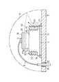
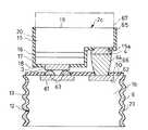
図1に概略的に示す実施例1に従う半導体発光装置は、基板1と、発光半導体領域2と、第1の電極3と、第2の電極4と、光透過性を有している包囲体5と、本発明に従う光反射層6と、金属支持板7と、端子8と、接続導体9とを備えている。以下、これ等を詳しく説明する。 A semiconductor light-emitting device according to Example 1 schematically shown in FIG. 1 includes a
基板1は、発光半導体領域2の機械的支持基板、及び発光半導体領域2の成長基板の機能を有し、一方の主面10と他方の主面11とこれ等の間の側面12とを備え、全体として四角柱状に形成されている。なお、もし、ウエーハを分割して基板1を得る時に側面12が傾斜すれば、基板1は四角錐台状になる。また、基板1を円柱状又は円錐台状又は四角形以外の角柱状又は角錐台状等に変形することができる。この実施例では、半導体発光装置のコストの低減を図るため及び基板1を電流通路として使用するために、基板1が導電性を有するシリコンで形成されている。シリコンは既に説明したようにサファイアよりも大きい光吸収率を有する。なお、基板1をシリコン以外のGaAs系化合物半導体、GaP系化合物半導体、金属、又は絶縁物で形成することができる。要するに、基板1が発光半導体領域2から放射された光を吸収する材料で形成されている全ての半導体発光装置に本発明を適用することができる。
本実施例では、基板1の側面12に図1で概略的に示す凹凸面(粗面)13が形成されている。この凹凸面13の詳細は追って説明する。The
In this embodiment, an uneven surface (rough surface) 13 schematically shown in FIG. 1 is formed on the
基板1の一方の主面10上に配置された発光半導体領域2はエピタキシャル成長領域又は主半導体領域と呼ぶこともできるものであって、バッファ層14とn型半導体層15と活性層16とp型半導体層17とを有する。
バッファ層14は、基板1の上にAlNとGaNとを交互に複数回エピタキシャル成長させた多層構造バッファである。勿論、AlN及びGaNの代りに別の窒化物半導体を使用して多層構造バッファを構成すること、又はバッファ層14をAlN等の窒化物半導体の単層バッファ層にすること、又はバッファ層14を省き、基板1の上にn型半導体層15を直接に形成することもできる。また、バッファ層14を発光半導体領域2の中に含めないで独立に示すこともできる。
n型半導体層15はn型クラッド層又は第1導電型半導体層と呼ぶこともできるものであって、バッファ層14の上に例えばn型窒化物半導体(例えばn型GaN)をエピタキシャル成長させることによって形成されている。
活性層16はダブルへテロ接合型半導体発光素子を構成するためのものであって、n型半導体層15の上に例えば不純物が添加されていない窒化物半導体(例えばInGaN)をエピタキシャル成長させることによって形成されている。図1では図示を簡略化するために活性層16が1つの層で示されているが、実際には周知の多重量子井戸構造を有している。勿論、活性層16を単一の半導体層とすることもできる。また、ダブルへテロ接合型半導体発光素子が要求されない場合には、活性層16を省いてn型半導体層15にp型半導体層17を直接に接触させることもできる。
p型半導体層17はp型クラッド層又は第2導電型半導体層と呼ぶこともできるものであって、活性層16の上に例えばp型窒化物半導体(例えばp型GaN)をエピタキシャル成長させることによって形成されている。なお、p型半導体層17の上に、更に、例えばp型窒化物半導体層(例えばp型GaN)から成る周知の電流分散層又はオーミックコンタクト層を配置することもできる。The light
The
The n-
The
The p-
発光半導体領域2は活性層16から発生した光の大部分を外部に取り出すための一方の主面18と基板1の一方の主面10に接触している他方の主面19と側面20とを有する。この実施例では活性層16から発生した光は発光半導体領域2の一方の主面18のみでなく、発光半導体領域2の側面20を通しても外部に取り出される。The light emitting
第1の電極3はアノード電極として機能するものであって、発光半導体領域2の一方の主面18の中央に形成され、接続導体9によって端子8に接続されている。第2の電極4はカソード電極として機能するものであって、基板1の他方の主面11に形成され、導電性接合材21によって金属支持板7に電気的及び機械的に結合されている。金属支持板7は、基板1及び発光半導体領域2の機械的支持機能を有する他に、電気的接続機能及び放熱機能を有する。なお、金属支持板7は、絶縁体22によって端子8から電気的に分離されている。The
鎖線で示す包囲体5は例えば1.5程度の光屈折率を有する光透過性保護樹脂(例えばエポキシ樹脂)から成り、基板1、発光半導体領域2、及び光反射層6を包囲している。The enclosure 5 indicated by a chain line is made of a light-transmitting protective resin (for example, epoxy resin) having a light refractive index of about 1.5, for example, and surrounds the
基板1の側面12の凹凸面(粗面)13はこの上に形成される光反射層6の凹凸面(粗面)23を得るためのものであり、多数の凹凸部を有する。基板1の側面12の凹凸面(粗面)13及び光反射層6の凹凸面(粗面)23における凹部は、光の散乱のために100nm〜10μmの深さ、200nm〜20μmの幅を有していることが望ましく、光の散乱効果をより大きく得るために0.5〜1.0μmの深さ、0.7〜1.5μmの幅を有していることがより望ましい。なお、光反射層6に光の散乱が要求されない場合は、基板1の側面12及び光反射層6の表面を平坦面とすることができる。The uneven surface (rough surface) 13 on the
図1に示す基板1及び発光半導体領域2はウエーハを切断することによって形成されている。即ち、図1に示す発光素子チップを得る時には、図1に示す基板1及び発光半導体領域2を複数個得ることができるウエーハを用意し、先ず、広い面積を有する発光半導体領域をエッチング(ドライエッチング又はウエットエッチング)によって複数の発光半導体領域2に分離する。次に、比較的太い幅(例えば40〜60μm)のブレード(刃)でウエーハの基板をハーフダイシングする。ウエーハの基板をブレード(刃)でダイシングすると、特別な粗面加工を伴わないで図1の基板1の側面12に概略的に示す凹凸面(粗面)13が得られる。凹凸面13における凹凸は100nm〜10μmの深さ、200nm〜20μmの幅を有する。図1においては図示を簡単にするために、凹凸面13を無視した場合における側面12の角度(平均角度)がほぼ垂直に示されているが、実際には例えば80〜85度の傾斜を有する。ハーフダイシングのためにウエーハの基板に例えば50〜100μm程度の未切断部分即ち残存部分が生じる。この残存部分は図1の光反射層6の形成工程後に、比較的細い幅(例えば30μm以下)のブレードで切断される。基板の残存部分を、周知のブレーキング法で切断することもできる。The
図1に説明的(概略的)に示す光反射層6は、基板1よりも反射率が大きい材料から成る。この光反射層6は、Al又はAl合金,Ag又はAg合金,Ti又はTi合金等の金属又は合金単層膜、又はこれらの多層膜、又は酸化物多層膜(例えば酸化ケイ素と酸化ジルコニアの多層膜)であることが望ましい。
この実施例では、ウエーハの基板をハーフダイシングした状態で、ウエーハの露出面に光反射材料を被着(例えば蒸着)し、しかる後フォトリソグラフィ工程で被着膜を選択的に除去することによって図1に示す光反射層6が形成されている。基板1の側面12の凹凸面13の上に光反射材料を被着すると、光反射層6にも基板1の側面12の凹凸面13に対応した光散乱用の凹凸面23が得られる。光反射層6における光散乱用の凹凸面23の凹凸の深さ及びピッチは基板1の側面12の凹凸面13の凹凸の深さ及びピッチとほぼ同一である。光反射層6の配置位置は、発光半導体領域2から包囲体5内に取り出され光の一部が、包囲体5の外周面(空気との界面)等で反射し、光反射層6に入射する位置に決定されている。
光反射層6の形成工程後に、ウエーハの基板の残存部分を切断して、図1に示す発光素子チップを得る。The
In this embodiment, with the wafer substrate half-diced, a light reflecting material is deposited (for example, vapor deposition) on the exposed surface of the wafer, and then the deposited film is selectively removed by a photolithography process. 1 is formed. When a light reflecting material is deposited on the
After the
本実施例によれば次の効果が得られる。
(1)図1において鎖線50で説明的に示すように発光半導体領域2から包囲体5内に取り出され、包囲体5の外周面(空気との界面)で反射し、光反射層6に至った光は、基板1の中に入り込まないで、光反射層6で反射され、包囲体5の中に戻され、外に取り出される。この結果、基板1における光吸収による損失が低減し、発光効率(光取り出し効率)が向上する。
(2)光反射層6が、見かけ上、光源のように機能するので、指向性の均一性が向上する。
(3)光反射層6に凹凸面23が形成されているので、この凹凸面23において光散乱が生じ、指向性の均一性が更に向上する。これにより、照明装置に好適な半導体発光装置を提供することができる。
(4)ブレードよるハーフダイシング時に生じる凹凸を利用して光反射層6の凹凸面23を形成するので、凹凸面23を容易に得ることができる。According to the present embodiment, the following effects can be obtained.
(1) As illustrated by a
(2) Since the
(3) Since the
(4) Since the
次に、図2に示す実施例2の半導体発光装置を説明する。但し、図2及び後述する図3〜図7において図1と実質的に同一の部分には同一の参照符号を付し、その説明を省略する。図2に示す実施例2の半導体発光装置は、変形された光反射層6aを有する点を除いて、図1の実施例1の半導体発光装置と同一に形成されている。 Next, the semiconductor light emitting device of Example 2 shown in FIG. 2 will be described. However, in FIG. 2 and FIGS. 3 to 7 described later, substantially the same parts as those in FIG. The semiconductor light emitting device of Example 2 shown in FIG. 2 is formed in the same manner as the semiconductor light emitting device of Example 1 of FIG. 1 except that it has a modified
図2の光反射層6aは基板1の側面12の一部のみでなく上方から見て露出した基板1の一方の主面10の一部上にも形成され、基板1の凹凸面13に対応した凹凸面23を有する。図2の光反射層6aは基板1の一方の主面10の一部にも形成されているので、図1の光反射層6よりも広い反射面積を有する。また、基板1の一方の主面10に図1に示す包囲体5から入射する光を基板1の上方に反射させることができる。従って、図2に示す実施例2の半導体発光装置によれば、前述の実施例1の効果(1)〜(4)を得らことができ、更に発光効率及びな指向性の均一化を改善することができる。The
図3に示す実施例3の半導体発光装置は、変形された発光半導体領域2aが設けられている点、追加の光反射層24が設けられている点及び、張り合わせ層25,26によって光反射層24を伴った発光半導体領域2aが基板1に張り合わせられている点を除いて、図1の実施例1の半導体発光装置と同一に形成されている。 The semiconductor light-emitting device of Example 3 shown in FIG. 3 is provided with a modified light-emitting
発光半導体領域2aは、図1の発光半導体領域2からバッファ層14を除いたものに相当する。追加の光反射層24は発光半導体領域2の他方の主面19に電気的及び機械的に結合されており、例えばAl,Ag等の金属層で形成され、基板1よりも大きい光反射率を有する。この光反射層24は第1及び第2の張り合わせ層25、26を介して基板1に結合されている。第1及び第2の張り合わせ層25、26は例えばAu等の金属から成る。The light emitting
図3に示す実施例3の半導体発光装置によれば、前述の実施例1の効果(1)〜(4)が得られるのみでなく、発光効率を更に向上させる効果も得られる。即ち、追加の光反射層24を有するので、活性層16から放射されて基板1に向う光が光反射層24で反射されて発光半導体領域2側に戻され、基板1で吸収されない。従って、発光効率が更に向上する。According to the semiconductor light emitting device of Example 3 shown in FIG. 3, not only the effects (1) to (4) of Example 1 described above can be obtained, but also the effect of further improving the light emission efficiency can be obtained. That is, since the additional light reflection layer 24 is provided, the light emitted from the
図4に示す実施例4の半導体発光装置は、基板1が傾斜側面12aを有する点を除いて、図1の実施例1の半導体発光装置と同一に形成されている。傾斜側面12aは、傾斜の強い(例えば45〜80度)のブレードを使用してウエーハ(基板)をハーフダイシング又はフルダイシングすることによって得られる。勿論、基板1の傾斜側面12aをエッチング等の別の方法で形成することもできる。基板1の傾斜側面12aを覆う光反射層6は、基板1の傾斜側面12aの凹凸面13に対応する凹凸面23を有し、基板1の側面12が垂直の場合に比べて光を上方に良好に反射する。この図4に示す実施例4によっても図1の実施例1と同様な効果を得ることができる。なお、図2及び図3の基板1が側面12を図4と同様な傾斜側面に変形することもできる。The semiconductor light emitting device of Example 4 shown in FIG. 4 is formed in the same manner as the semiconductor light emitting device of Example 1 of FIG. 1 except that the
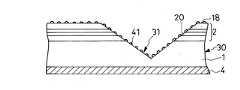
図5は実施例5の半導体発光装置の製造方法を示す。この実施例5では、エッチングによって基板1及び発光半導体領域2を含むウエーハ30にV字状溝31が形成されている。このV字状溝31の壁面に光散乱用の凹凸面(粗面)を得るために多数の開口33を有するレジストマスク32がV字状溝31の側壁及び発光半導体領域2の主面に形成されている。図5に示すものにドライエッチング(例えばプラズマエッチング)又はウエットエッチングを施すと、レジストマスク32の開口33を通して基板1がエッチングされ、図1に示した凹凸面(粗面)13と同様なものが基板1のV字状溝31の壁面に得られる。しかる後、図1の光反射層6と同様なものを形成し、ウエーハ30を個別チップに分割する。これにより、図1の実施例1と同様な効果を有する半導体発光装置を提供することができる。なお、図5のV字状溝31をブレードで形成することもできる。また、図3の光反射層24に相当するものを図5の半導体発光装置に設けることができる。FIG. 5 shows a method for manufacturing the semiconductor light-emitting device of Example 5. In the fifth embodiment, a V-shaped
図6は実施例6の半導体発光装置の製造方法を示す。この実施例6では、図5と同様にV字状溝31を形成した後に、Ag(銀)の凝集を利用してV字状溝31の側壁及び発光半導体領域2の主面に多数の粒状体(凝集体)41を形成し、この多数の粒状体(凝集体)41をマスクとして使用してエッチング(ドライエッチング)することによってV字状溝31の側壁及び発光半導体領域2の主面に凹凸面(粗面)を形成する。この凝集体を使用して凹凸面(粗面)を形成する方法の詳細を次に説明する。FIG. 6 shows a method for manufacturing the semiconductor light emitting device of Example 6. In Example 6, after forming the V-shaped
図6のAgの粒状体(凝集体)41を形成するために、先ず、ウエーハ30の一方の主面即ちV字状溝31の側壁及び発光半導体領域2の主面18に熱処理によって粒状化即ち凝集し易い金属材料であるAgを例えば真空蒸着装置を使用して被着させる。図6では発光半導体領域2の主面18及び側面20にも粒状体(凝集体)41が形成されているが、発光半導体領域2に凹凸面(粗面)を形成することが不要の場合には、基板1の溝31の側壁以外をレジストで覆うことができる。Ag膜の好ましい厚みは2〜100nm(20〜1000Å)、より好ましい厚みは10〜30nmであり、この実施例における厚みは20nmである。Ag膜の厚みは目標とする粒子の大きさによって調整される。Ag膜の厚みが100nmよりも厚くなると、粒状体(凝集体)と粒状体(凝集体)とが繋がるような凝集不良が多くなり、また2nmよりも薄くなると、目標とする大きさの粒子を得ることが困難になる。なお、Ag膜の代わりにAg合金、又はAl(アルミニウム)、又はCu(銅)、又はAu(金)、又はこれらの合金から成る膜を形成することもできる。また、Ag膜を周知のスパッタリング方法、電子ビーム蒸着方法、塗布等の別の方法で形成することもできる。In order to form the Ag granules (aggregates) 41 in FIG. 6, first, one main surface of the
この実施例では真空蒸着法でAg膜を形成する時のウエーハ30の温度を室温としたが、室温〜150℃位にすることもできる。また、Ag膜を形成する時のウエーハ30の温度をAg膜が凝集する温度(例えば150〜500℃)とし、Ag膜形成と同時に凝集させることができる。
次に、Ag膜を伴ったウエーハ30を半導体の分野で一般に使用されている熱処理炉に入れて、Ag膜を伴ったウエーハ30に対して大気中で例えば300℃の熱処理を施してAg膜を図3に概略的に示す多数の粒状体(凝集体)41に変化させる。熱処理でAgを凝集させるための好ましい温度は250〜350℃である。In this embodiment, the temperature of the
Next, the
多数の粒状体41は、溝31の側壁及び発光半導体領域2の主面18上に不規則に分布する。粒状体41の粒径はAg膜の厚みに比例的に変化する。Ag膜の厚みが20nmの場合には、粒径は50〜200nmの範囲であり、平均粒径は約130nmである。もし、Ag膜の厚みが50nmよりも厚くなると、凝集のための加熱処理を施しても独立した多数の粒状体41を形成することが困難になり、粒状体41の相互間の繋がりが生じ、Agが網目状に分布した状態が生じる。また、Ag膜の厚みが100nmよりも厚い時には、熱処理を施した時にウエーハ30の主面上にAgの厚い部分が網目状に生じ、この厚い部分以外が薄いAgで覆われ、マスクとして使用可能な粒状体(凝集体)が得られない。従って、Ag膜の好ましい厚みの範囲は前述した2〜100nmである。厚み20nmのAg膜の凝集に基づく粒状体41の1μm2当たりの個数は4〜15である。粒状体41の単位面積当たりの個数はAg膜の厚みに対して反比例的に変化する。粒状体41はウエーハ30の表面上に不規則に分布するが、ウエーハ30の表面全体で見ると、比較的均一性のよい状態で分布する。A large number of the
図3に示すように粒状体(Ag粒)41は、ウエーハ30の選択的エッチングのマスクとしての機能を有する。即ち、粒状体41をマスクとしてウエーハ30の露出面を選択的エッチングすることができる。そこで、本実施例では、周知のドライエッチング(プラズマエッチング)法でウエーハ30の粒状体41で覆われていない部分を10〜30min程度の時間エッチングして図1に説明的に示す凹凸面13に相当するものを形成する。図6の方法では発光半導体領域2の主面18及び側面20にも凹凸面が生じる。この凹凸面は発光半導体領域2と包囲体5との間の全反射を抑制し、発光効率を向上するために寄与する。
次に、ドライエッチング後のAgから成る粒状体41を、Agのためのエッチング液、例えば、塩化水素(HCl)と水とからなるエッチング液、又は水酸化アンモニウム(NH4OH)と過酸化水素(H2O2)と水(H2O)とから成るエッチング液によって室温で2分間エッチング処理して除去する。As shown in FIG. 3, the granular material (Ag particle) 41 functions as a mask for selective etching of the
Next, the
図1に説明的(概略的)に示す光反射層6を得る時には、図6に示すウエーハ30における基板1及び発光半導体領域2の露出面に光反射材料を被着(例えば蒸着)し、しかる後フォトリソグラフィ工程で被着膜を選択的に除去する。基板1の側面12に凹凸面13が形成されているので、図1に示す光反射層6と同様なものにも基板1の側面12に凹凸面13に対応した光散乱用の凹凸面23が得られる。しかる後、ウエーハ30を溝31で分断し、複数のチップを得る。
図6の実施例6は、図1の実施例1と同様な効果を有する他に、粒状体(凝集体)41を使用して光反射層に凹凸面を容易に形成できるという効果も有する。When obtaining the
Example 6 in FIG. 6 has the same effect as that in Example 1 in FIG. 1 and also has an effect that the irregular surface can be easily formed on the light reflection layer using the granular material (aggregate) 41.
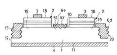
図7に示す実施例7の半導体発光装置は、1つの基板1の上に複数の発光半導体領域2を有する点、及び基板1の主面10に凹凸面51を有し、この凹凸面51の上に光散乱用の凹凸面52を有する光反射層6eを有する点を除いて、図1の実施例1の半導体発光装置と同一に形成されている。なお、基板1の側面12及び基板1の主面に延在する部分に図2と同様に光散乱用の凹凸面23を有する光反射層6dが形成されている。
図7に示す実施例7は、図1及び図2の実施例1及び2と同様な効果を有する他に、複数の発光半導体領域2の相互間の光反射層6eによって光散乱効果が更に良くなり、光の指向性の均一化が更に良くなるという効果を有する。The semiconductor light-emitting device of Example 7 shown in FIG. 7 has a plurality of light-emitting
The
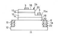
図8に示す実施例8の半導体発光装置は、変形された発光半導体領域2bを設けた点、第2の電極4の形成位置を変えた点、絶縁性基板1aを設けた点を除いて図1の実施例1の半導体発光装置と同様に形成されている。発光半導体領域2bは段部15aを有する。この段部15aはn型半導体領域15及びバッファ層14を、活性層16及びp型半導体層17よりも横方向に突出させることによって形成されている。第2の電極4は段部15aに配置され、n型半導体層15に接続されている。発光半導体領域2bは絶縁性基板1a上に配置されている。
なお、バッファ層14に段部15aと同様なものを形成し、ここに第2の電極4を接続することもできる。また、基板1aを導電性基板とすることもできる。
図8の実施例8においても基板1aの側面12に光反射層6が図1と同様に形成されているので、実施例1と同様な効果を得ることができる。また、第1及び第2の電極3,4が同一方向に露出しているので、外部回路への接続が容易になる。また、n型半導体層15に第2の電極4を接続したので、第1及び第2の電極3,4間の抵抗値が小さくなる。
なお、図2〜図7の実施例2〜7にも図8の第2の電極4の配置を適用することができる。The semiconductor light emitting device of Example 8 shown in FIG. 8 is a diagram except that the modified light emitting
Alternatively, the
Also in Example 8 of FIG. 8, since the
The arrangement of the
図9に示す実施例9の半導体発光装置は、変形された発光半導体領域2cを設けた点、絶縁性基板1bを設けた点、及び発光半導体領域2cと基板1bとの接続形態を変えた点を除いて図1と同様に形成されている。
図9の発光半導体領域2cは、段部15aを有する点、及びバッファ層14を有さない点で図1の発光半導体領域2と相違している。第2の電極4は発光半導体領域2cの段部15aに設けられている。絶縁性基板1bの一方の主面10に第1及び第2の導体層61,62が設けられている。発光半導体領域2cの一方の主面18の第1の電極3はバンプ電極63を介して基板1bの第1の導体層61に電気的及び機械的に結合されている。発光半導体領域2cの段部15aの第2の電極4はバンプ電極64を介して基板1bの第2の導体層62に電気的及び機械的に結合されている。図9の半導体発光装置においては、発光半導体領域2cの他方の主面19側から包囲体(図示せず)中に光が取り出される。
発光半導体領域2cの一方の主面18及び側面20に絶縁膜65が設けられている。基板1bの一方の主面10にも選択的に絶縁膜66が設けられている。図9の実施例9の半導体発光装置においては、基板1bの側面12の全部に光反射層6が設けられている。
なお、発光半導体領域2cの他方の主面19に鎖線で示すように光透過性基板67を設けることができる。In the semiconductor light emitting device of Example 9 shown in FIG. 9, the modified light emitting
The light emitting
An insulating
A
図9の実施例9の半導体装置は、実施例1と同様な光反射層6を有するので、実施例1と同様な効果を得ることができる。なお、図2〜7の実施例2〜7にも図9のバンプ電極63、64による結合構造を適用できる。 Since the semiconductor device of Example 9 in FIG. 9 has the
本発明は上述の実施例に限定されるものでなく、例えば次の変形が可能なものである。
(1)発光半導体領域2,2aを、AlGaInP,AlGaAS,GaP等の別の材料にすることができる。
(2)発光半導体領域2,2aの一方の主面18上に例えばITOからなる光透過性導電膜を設け、光透過性導電膜の表面に全反射防止用の粗面を形成することができる。
(3)図3に示す追加に光反射層24を図2、図4〜図9の実施例2,4〜9にも適用することができる。
(4)ウエーハをハーフダイシングする代わりにフルダイシングすることができる。なお、ウエーハ(基板)をフルダイシングする時には、フルダイシング後にウエーハが複数のチップに分離されることを防ぐためにウエーハの下面にダイシングテープ(粘着テープ)を貼り付けておくことが望ましい。
(5)基板1の側面12に凹凸面13を形成するために例えばフッ酸と硝酸と水から成る液で基板1の側面12をウェットエッチングすることができる。The present invention is not limited to the above-described embodiments, and for example, the following modifications are possible.
(1) The light emitting
(2) A light-transmitting conductive film made of, for example, ITO can be provided on one
(3) In addition, the light reflecting layer 24 can be applied to the second and fourth to fourth embodiments shown in FIGS. 2 and 4 to 9.
(4) Full dicing can be performed instead of half dicing the wafer. When the wafer (substrate) is fully diced, it is desirable to attach a dicing tape (adhesive tape) to the lower surface of the wafer in order to prevent the wafer from being separated into a plurality of chips after full dicing.
(5) In order to form the
1 基板
2 発光半導体領域
6 光反射層
23 凹凸面DESCRIPTION OF
Claims (12)
Translated fromJapanese前記基板の前記一方の主面上に配置された発光半導体領域と、
前記発光半導体領域に電気的に接続された第1及び第2の電極と、
前記基板及び前記発光半導体領域を包囲し且つ光透過性を有している包囲体と、
前記包囲体で包囲されている前記基板の表面の少なくとも一部に配置され、且つこの配置位置が前記発光半導体領域から前記包囲体内に放射された光の一部が入射することが可能な位置に決定されている光反射層と
を備えていることを特徴とする半導体発光装置。A substrate having one main surface and the other main surface and side surfaces;
A light emitting semiconductor region disposed on the one main surface of the substrate;
First and second electrodes electrically connected to the light emitting semiconductor region;
An enclosure that surrounds the substrate and the light emitting semiconductor region and has light transparency;
It is arranged on at least a part of the surface of the substrate surrounded by the enclosure, and this arrangement position is a position where a part of the light emitted from the light emitting semiconductor region into the enclosure can enter. A semiconductor light emitting device comprising: a determined light reflecting layer.
前記第1の電極は前記発光半導体領域の一方の主面に接続され、前記第2の電極は前記基板に接続されていることを特徴とする請求項1乃至9のいずれか1つに記載の半導体発光装置。The substrate has electrical conductivity;
10. The device according to claim 1, wherein the first electrode is connected to one main surface of the light emitting semiconductor region, and the second electrode is connected to the substrate. Semiconductor light emitting device.
Priority Applications (4)
| Application Number | Priority Date | Filing Date | Title |
|---|---|---|---|
| JP2007165261AJP2009004625A (en) | 2007-06-22 | 2007-06-22 | Semiconductor light emitting device |
| TW097118383ATW200913318A (en) | 2007-06-22 | 2008-05-19 | Semiconductor light emitting device |
| KR1020080054063AKR100950137B1 (en) | 2007-06-22 | 2008-06-10 | Semiconductor light emitting device |
| US12/141,273US8120049B2 (en) | 2007-06-22 | 2008-06-18 | Light-emitting semiconductor device |
Applications Claiming Priority (1)
| Application Number | Priority Date | Filing Date | Title |
|---|---|---|---|
| JP2007165261AJP2009004625A (en) | 2007-06-22 | 2007-06-22 | Semiconductor light emitting device |
Publications (1)
| Publication Number | Publication Date |
|---|---|
| JP2009004625Atrue JP2009004625A (en) | 2009-01-08 |
Family
ID=40135541
Family Applications (1)
| Application Number | Title | Priority Date | Filing Date |
|---|---|---|---|
| JP2007165261APendingJP2009004625A (en) | 2007-06-22 | 2007-06-22 | Semiconductor light emitting device |
Country Status (4)
| Country | Link |
|---|---|
| US (1) | US8120049B2 (en) |
| JP (1) | JP2009004625A (en) |
| KR (1) | KR100950137B1 (en) |
| TW (1) | TW200913318A (en) |
Cited By (4)
| Publication number | Priority date | Publication date | Assignee | Title |
|---|---|---|---|---|
| WO2010095353A1 (en)* | 2009-02-20 | 2010-08-26 | 昭和電工株式会社 | Light-emitting diode, method for producing same, and light-emitting diode lamp |
| JP2011100905A (en)* | 2009-11-09 | 2011-05-19 | Nichia Corp | Light emitting device and method of manufacturing the same |
| JPWO2014167745A1 (en)* | 2013-04-10 | 2017-02-16 | 三菱電機株式会社 | Semiconductor device and method for manufacturing semiconductor device |
| WO2018139769A1 (en)* | 2017-01-26 | 2018-08-02 | 서울바이오시스 주식회사 | Light emitting diode including light emitting cells |
Families Citing this family (21)
| Publication number | Priority date | Publication date | Assignee | Title |
|---|---|---|---|---|
| JP2008270416A (en)* | 2007-04-18 | 2008-11-06 | Sanken Electric Co Ltd | Method for forming a rough surface on an object |
| TWI423467B (en) | 2007-06-06 | 2014-01-11 | Epistar Corp | Semiconductor light emitting device |
| US20100327300A1 (en)* | 2009-06-25 | 2010-12-30 | Koninklijke Philips Electronics N.V. | Contact for a semiconductor light emitting device |
| KR101020995B1 (en)* | 2010-02-18 | 2011-03-09 | 엘지이노텍 주식회사 | Light emitting device, light emitting device manufacturing method and light emitting device package |
| KR101014155B1 (en)* | 2010-03-10 | 2011-02-10 | 엘지이노텍 주식회사 | Light emitting device, light emitting device manufacturing method and light emitting device package |
| DE102010036180A1 (en) | 2010-09-02 | 2012-03-08 | Osram Opto Semiconductors Gmbh | LED chip |
| JP2013110154A (en)* | 2011-11-17 | 2013-06-06 | Sanken Electric Co Ltd | Light emitting device |
| JP5644745B2 (en)* | 2011-12-05 | 2014-12-24 | 豊田合成株式会社 | Semiconductor light emitting element and light emitting device |
| CN103199183B (en)* | 2013-04-08 | 2016-01-27 | 厦门市三安光电科技有限公司 | A kind of encapsulating structure improving vertical LED chip brightness |
| CN103199184B (en)* | 2013-04-08 | 2016-04-20 | 厦门市三安光电科技有限公司 | A kind of encapsulating structure improving vertical LED chip brightness |
| WO2014184701A1 (en)* | 2013-05-15 | 2014-11-20 | Koninklijke Philips N.V. | Led with scattering features in substrate |
| DE102013107967B4 (en)* | 2013-07-25 | 2021-05-06 | OSRAM Opto Semiconductors Gesellschaft mit beschränkter Haftung | Optoelectronic semiconductor chip, optoelectronic component and method for producing a plurality of optoelectronic semiconductor chips |
| JP2015028984A (en)* | 2013-07-30 | 2015-02-12 | 日亜化学工業株式会社 | Semiconductor light emitting element |
| JP6255192B2 (en)* | 2013-09-04 | 2017-12-27 | 株式会社ディスコ | Optical device and processing method of optical device |
| DE102013111503B4 (en)* | 2013-10-18 | 2021-08-05 | OSRAM Opto Semiconductors Gesellschaft mit beschränkter Haftung | Optoelectronic semiconductor chip, optoelectronic component and method for separating semiconductor chips |
| TWI506824B (en)* | 2013-10-28 | 2015-11-01 | Lextar Electronics Corp | Light-emitting diode package structure and manufacturing method thereof |
| JP6250429B2 (en)* | 2014-02-13 | 2017-12-20 | エスアイアイ・セミコンダクタ株式会社 | Semiconductor device and manufacturing method thereof |
| US20160079217A1 (en)* | 2014-09-12 | 2016-03-17 | Kabushiki Kaisha Toshiba | Semiconductor light emitting device and lead frame |
| JP6547562B2 (en)* | 2015-09-30 | 2019-07-24 | 日亜化学工業株式会社 | Light source device |
| DE102019106931A1 (en) | 2019-03-19 | 2020-09-24 | OSRAM Opto Semiconductors Gesellschaft mit beschränkter Haftung | Optoelectronic semiconductor component, optoelectronic semiconductor device and method for producing an optoelectronic semiconductor component |
| CN113192883A (en)* | 2021-04-20 | 2021-07-30 | 天津三安光电有限公司 | Infrared light-emitting diode and preparation method thereof |
Citations (11)
| Publication number | Priority date | Publication date | Assignee | Title |
|---|---|---|---|---|
| JPH10270754A (en)* | 1997-03-24 | 1998-10-09 | Sanyo Electric Co Ltd | Semiconductor light-emitting device and light-emitting lamp |
| JP2002009349A (en)* | 2000-06-26 | 2002-01-11 | Koha Co Ltd | LED surface light emitting device and method of manufacturing the same |
| JP2004319915A (en)* | 2003-04-18 | 2004-11-11 | Sharp Corp | Semiconductor laser device manufacturing method and semiconductor laser device |
| JP2006041133A (en)* | 2004-07-26 | 2006-02-09 | Matsushita Electric Ind Co Ltd | Light emitting device |
| JP2006173271A (en)* | 2004-12-14 | 2006-06-29 | Matsushita Electric Ind Co Ltd | Semiconductor light emitting device, lighting device, portable communication device, and camera |
| JP2006253298A (en)* | 2005-03-09 | 2006-09-21 | Toshiba Corp | Semiconductor light emitting device and semiconductor light emitting device |
| JP2006303525A (en)* | 2006-06-09 | 2006-11-02 | Rohm Co Ltd | Semiconductor light emitting device |
| JP2006344564A (en)* | 2005-06-10 | 2006-12-21 | Citizen Electronics Co Ltd | LED light source unit |
| JP2007013107A (en)* | 2005-05-31 | 2007-01-18 | Sanyo Electric Co Ltd | Semiconductor light emitting device and semiconductor light emitting device |
| JP2007116125A (en)* | 2005-09-20 | 2007-05-10 | Matsushita Electric Works Ltd | Light emitting device |
| JP2007123436A (en)* | 2005-10-26 | 2007-05-17 | Toshiba Corp | Semiconductor light emitting device and manufacturing method thereof |
Family Cites Families (13)
| Publication number | Priority date | Publication date | Assignee | Title |
|---|---|---|---|---|
| JPH0774395A (en)* | 1993-08-31 | 1995-03-17 | Victor Co Of Japan Ltd | Light emitting diode device and its manufacturing method |
| US5710441A (en)* | 1995-10-30 | 1998-01-20 | Motorola, Inc. | Microcavity LED with photon recycling |
| US6091195A (en)* | 1997-02-03 | 2000-07-18 | The Trustees Of Princeton University | Displays having mesa pixel configuration |
| JP3769872B2 (en)* | 1997-05-06 | 2006-04-26 | ソニー株式会社 | Semiconductor light emitting device |
| JP2000031540A (en)* | 1999-06-18 | 2000-01-28 | Toyoda Gosei Co Ltd | Manufacture of gallium nitride based compound semiconductor light emitting element |
| US6630689B2 (en)* | 2001-05-09 | 2003-10-07 | Lumileds Lighting, U.S. Llc | Semiconductor LED flip-chip with high reflectivity dielectric coating on the mesa |
| JP2004055816A (en) | 2002-07-19 | 2004-02-19 | Sanyo Electric Co Ltd | Nitride compound semiconductor light emitting device and method of manufacturing the same |
| TW200522397A (en) | 2003-11-04 | 2005-07-01 | Shinetsu Handotai Kk | Light-emitting device |
| JP2005277372A (en) | 2004-02-25 | 2005-10-06 | Sanken Electric Co Ltd | Semiconductor light emitting device and manufacturing method thereof |
| JP2005327979A (en) | 2004-05-17 | 2005-11-24 | Toshiba Corp | Semiconductor light emitting element and semiconductor light emitting device |
| KR20060077801A (en)* | 2004-12-31 | 2006-07-05 | 엘지전자 주식회사 | High power light emitting diode and its manufacturing method |
| US20060228094A1 (en)* | 2005-04-08 | 2006-10-12 | Upstream Engineering Oy | Method for manufacturing beam-shaping components |
| KR20080028071A (en)* | 2006-09-26 | 2008-03-31 | 서울옵토디바이스주식회사 | LED device having a light reflection pattern at the rear |
- 2007
- 2007-06-22JPJP2007165261Apatent/JP2009004625A/enactivePending
- 2008
- 2008-05-19TWTW097118383Apatent/TW200913318A/ennot_activeIP Right Cessation
- 2008-06-10KRKR1020080054063Apatent/KR100950137B1/ennot_activeExpired - Fee Related
- 2008-06-18USUS12/141,273patent/US8120049B2/ennot_activeExpired - Fee Related
Patent Citations (11)
| Publication number | Priority date | Publication date | Assignee | Title |
|---|---|---|---|---|
| JPH10270754A (en)* | 1997-03-24 | 1998-10-09 | Sanyo Electric Co Ltd | Semiconductor light-emitting device and light-emitting lamp |
| JP2002009349A (en)* | 2000-06-26 | 2002-01-11 | Koha Co Ltd | LED surface light emitting device and method of manufacturing the same |
| JP2004319915A (en)* | 2003-04-18 | 2004-11-11 | Sharp Corp | Semiconductor laser device manufacturing method and semiconductor laser device |
| JP2006041133A (en)* | 2004-07-26 | 2006-02-09 | Matsushita Electric Ind Co Ltd | Light emitting device |
| JP2006173271A (en)* | 2004-12-14 | 2006-06-29 | Matsushita Electric Ind Co Ltd | Semiconductor light emitting device, lighting device, portable communication device, and camera |
| JP2006253298A (en)* | 2005-03-09 | 2006-09-21 | Toshiba Corp | Semiconductor light emitting device and semiconductor light emitting device |
| JP2007013107A (en)* | 2005-05-31 | 2007-01-18 | Sanyo Electric Co Ltd | Semiconductor light emitting device and semiconductor light emitting device |
| JP2006344564A (en)* | 2005-06-10 | 2006-12-21 | Citizen Electronics Co Ltd | LED light source unit |
| JP2007116125A (en)* | 2005-09-20 | 2007-05-10 | Matsushita Electric Works Ltd | Light emitting device |
| JP2007123436A (en)* | 2005-10-26 | 2007-05-17 | Toshiba Corp | Semiconductor light emitting device and manufacturing method thereof |
| JP2006303525A (en)* | 2006-06-09 | 2006-11-02 | Rohm Co Ltd | Semiconductor light emitting device |
Cited By (7)
| Publication number | Priority date | Publication date | Assignee | Title |
|---|---|---|---|---|
| WO2010095353A1 (en)* | 2009-02-20 | 2010-08-26 | 昭和電工株式会社 | Light-emitting diode, method for producing same, and light-emitting diode lamp |
| JP2010192835A (en)* | 2009-02-20 | 2010-09-02 | Showa Denko Kk | Light emitting diode, method for manufacturing the same, and light emitting diode lamp |
| KR101290836B1 (en) | 2009-02-20 | 2013-07-29 | 도요다 고세이 가부시키가이샤 | Light-emitting diode, method for producing same, and light-emitting diode lamp |
| JP2011100905A (en)* | 2009-11-09 | 2011-05-19 | Nichia Corp | Light emitting device and method of manufacturing the same |
| JPWO2014167745A1 (en)* | 2013-04-10 | 2017-02-16 | 三菱電機株式会社 | Semiconductor device and method for manufacturing semiconductor device |
| US11233029B2 (en) | 2013-04-10 | 2022-01-25 | Mitsubishi Electric Corporation | Semiconductor device having a device fixed on a substrate with an adhesive |
| WO2018139769A1 (en)* | 2017-01-26 | 2018-08-02 | 서울바이오시스 주식회사 | Light emitting diode including light emitting cells |
Also Published As
| Publication number | Publication date |
|---|---|
| TWI365548B (en) | 2012-06-01 |
| US20080315232A1 (en) | 2008-12-25 |
| KR100950137B1 (en) | 2010-03-30 |
| US8120049B2 (en) | 2012-02-21 |
| TW200913318A (en) | 2009-03-16 |
| KR20080112947A (en) | 2008-12-26 |
Similar Documents
| Publication | Publication Date | Title |
|---|---|---|
| JP2009004625A (en) | Semiconductor light emitting device | |
| US10978618B2 (en) | Semiconductor light emitting device | |
| US8969897B2 (en) | Light emitting device | |
| JP5949294B2 (en) | Semiconductor light emitting device | |
| JP3326545B2 (en) | Semiconductor light emitting device | |
| JP6023660B2 (en) | Semiconductor light emitting device and semiconductor light emitting device | |
| KR102323686B1 (en) | Light emitting device and method of fabricating the same | |
| KR101017394B1 (en) | Light emitting device and method of manufacturing the same | |
| KR100887139B1 (en) | Nitride semiconductor light emitting device and manufacturing method | |
| CN100420041C (en) | Radiation-emitting semiconductor devices | |
| JP5304662B2 (en) | Light emitting element | |
| CN100590898C (en) | Positive electrode for semiconductor light emitting devices | |
| US8492780B2 (en) | Light-emitting device and manufacturing method thereof | |
| US20060011935A1 (en) | Light extraction from a semiconductor light emitting device via chip shaping | |
| CN105009308B (en) | Method and apparatus for creating porous reflective contact part | |
| JP3737494B2 (en) | Semiconductor light emitting device, method for manufacturing the same, and semiconductor light emitting device | |
| KR101228130B1 (en) | Semiconductor light-emitting element, manufacturing method, and light-emiting device | |
| JP2008218878A (en) | GaN-based LED element and light emitting device | |
| CN101901862A (en) | Semiconductor light emitting element | |
| JP2011060966A (en) | Light-emitting device | |
| CN111106212A (en) | Deep ultraviolet light-emitting diode with vertical structure and preparation method thereof | |
| KR20100137524A (en) | How to form light emitting diode structure, lamp device and light emitting diode structure | |
| JP2008198876A (en) | GaN-based LED element and light emitting device | |
| KR20130065451A (en) | Light emitting device | |
| JP5123221B2 (en) | Light emitting device |
Legal Events
| Date | Code | Title | Description |
|---|---|---|---|
| A621 | Written request for application examination | Free format text:JAPANESE INTERMEDIATE CODE: A621 Effective date:20100602 | |
| A977 | Report on retrieval | Free format text:JAPANESE INTERMEDIATE CODE: A971007 Effective date:20120213 | |
| A131 | Notification of reasons for refusal | Free format text:JAPANESE INTERMEDIATE CODE: A131 Effective date:20120221 | |
| A521 | Request for written amendment filed | Free format text:JAPANESE INTERMEDIATE CODE: A523 Effective date:20120406 | |
| A131 | Notification of reasons for refusal | Free format text:JAPANESE INTERMEDIATE CODE: A131 Effective date:20120424 | |
| A02 | Decision of refusal | Free format text:JAPANESE INTERMEDIATE CODE: A02 Effective date:20120816 |