JP2008530599A - Drive circuit for organic light emitting diode display with current programming - Google Patents
Drive circuit for organic light emitting diode display with current programmingDownload PDFInfo
- Publication number
- JP2008530599A JP2008530599AJP2007554402AJP2007554402AJP2008530599AJP 2008530599 AJP2008530599 AJP 2008530599AJP 2007554402 AJP2007554402 AJP 2007554402AJP 2007554402 AJP2007554402 AJP 2007554402AJP 2008530599 AJP2008530599 AJP 2008530599A
- Authority
- JP
- Japan
- Prior art keywords
- current
- emitting diode
- light emitting
- current source
- drive circuit
- Prior art date
- Legal status (The legal status is an assumption and is not a legal conclusion. Google has not performed a legal analysis and makes no representation as to the accuracy of the status listed.)
- Granted
Links
- 230000003071parasitic effectEffects0.000claimsabstractdescription22
- 238000012544monitoring processMethods0.000claimsabstractdescription5
- 238000000034methodMethods0.000claimsdescription15
- 239000010409thin filmSubstances0.000claimsdescription3
- 230000006641stabilisationEffects0.000description14
- 238000011105stabilizationMethods0.000description14
- 238000010586diagramMethods0.000description6
- 239000010410layerSubstances0.000description5
- 238000005516engineering processMethods0.000description4
- 239000003990capacitorSubstances0.000description3
- 230000004044responseEffects0.000description3
- 229920001621AMOLEDPolymers0.000description2
- 229910021417amorphous siliconInorganic materials0.000description2
- 239000012044organic layerSubstances0.000description2
- 230000015556catabolic processEffects0.000description1
- 230000008859changeEffects0.000description1
- 238000006731degradation reactionMethods0.000description1
- 239000011521glassSubstances0.000description1
- 230000005525hole transportEffects0.000description1
- 230000006872improvementEffects0.000description1
- 238000002347injectionMethods0.000description1
- 239000007924injectionSubstances0.000description1
- 238000011835investigationMethods0.000description1
- 230000035800maturationEffects0.000description1
- 239000002184metalSubstances0.000description1
- 230000000116mitigating effectEffects0.000description1
- 238000012986modificationMethods0.000description1
- 230000004048modificationEffects0.000description1
- 230000008569processEffects0.000description1
- 230000009467reductionEffects0.000description1
- 230000004043responsivenessEffects0.000description1
- 239000000243solutionSubstances0.000description1
Images


Classifications
- G—PHYSICS
- G09—EDUCATION; CRYPTOGRAPHY; DISPLAY; ADVERTISING; SEALS
- G09G—ARRANGEMENTS OR CIRCUITS FOR CONTROL OF INDICATING DEVICES USING STATIC MEANS TO PRESENT VARIABLE INFORMATION
- G09G3/00—Control arrangements or circuits, of interest only in connection with visual indicators other than cathode-ray tubes
- G09G3/20—Control arrangements or circuits, of interest only in connection with visual indicators other than cathode-ray tubes for presentation of an assembly of a number of characters, e.g. a page, by composing the assembly by combination of individual elements arranged in a matrix no fixed position being assigned to or needed to be assigned to the individual characters or partial characters
- G09G3/22—Control arrangements or circuits, of interest only in connection with visual indicators other than cathode-ray tubes for presentation of an assembly of a number of characters, e.g. a page, by composing the assembly by combination of individual elements arranged in a matrix no fixed position being assigned to or needed to be assigned to the individual characters or partial characters using controlled light sources
- G09G3/30—Control arrangements or circuits, of interest only in connection with visual indicators other than cathode-ray tubes for presentation of an assembly of a number of characters, e.g. a page, by composing the assembly by combination of individual elements arranged in a matrix no fixed position being assigned to or needed to be assigned to the individual characters or partial characters using controlled light sources using electroluminescent panels
- G09G3/32—Control arrangements or circuits, of interest only in connection with visual indicators other than cathode-ray tubes for presentation of an assembly of a number of characters, e.g. a page, by composing the assembly by combination of individual elements arranged in a matrix no fixed position being assigned to or needed to be assigned to the individual characters or partial characters using controlled light sources using electroluminescent panels semiconductive, e.g. using light-emitting diodes [LED]
- G09G3/3208—Control arrangements or circuits, of interest only in connection with visual indicators other than cathode-ray tubes for presentation of an assembly of a number of characters, e.g. a page, by composing the assembly by combination of individual elements arranged in a matrix no fixed position being assigned to or needed to be assigned to the individual characters or partial characters using controlled light sources using electroluminescent panels semiconductive, e.g. using light-emitting diodes [LED] organic, e.g. using organic light-emitting diodes [OLED]
- G09G3/3275—Details of drivers for data electrodes
- G09G3/3283—Details of drivers for data electrodes in which the data driver supplies a variable data current for setting the current through, or the voltage across, the light-emitting elements
- G—PHYSICS
- G09—EDUCATION; CRYPTOGRAPHY; DISPLAY; ADVERTISING; SEALS
- G09G—ARRANGEMENTS OR CIRCUITS FOR CONTROL OF INDICATING DEVICES USING STATIC MEANS TO PRESENT VARIABLE INFORMATION
- G09G3/00—Control arrangements or circuits, of interest only in connection with visual indicators other than cathode-ray tubes
- G09G3/20—Control arrangements or circuits, of interest only in connection with visual indicators other than cathode-ray tubes for presentation of an assembly of a number of characters, e.g. a page, by composing the assembly by combination of individual elements arranged in a matrix no fixed position being assigned to or needed to be assigned to the individual characters or partial characters
- G09G3/22—Control arrangements or circuits, of interest only in connection with visual indicators other than cathode-ray tubes for presentation of an assembly of a number of characters, e.g. a page, by composing the assembly by combination of individual elements arranged in a matrix no fixed position being assigned to or needed to be assigned to the individual characters or partial characters using controlled light sources
- G09G3/30—Control arrangements or circuits, of interest only in connection with visual indicators other than cathode-ray tubes for presentation of an assembly of a number of characters, e.g. a page, by composing the assembly by combination of individual elements arranged in a matrix no fixed position being assigned to or needed to be assigned to the individual characters or partial characters using controlled light sources using electroluminescent panels
- G09G3/32—Control arrangements or circuits, of interest only in connection with visual indicators other than cathode-ray tubes for presentation of an assembly of a number of characters, e.g. a page, by composing the assembly by combination of individual elements arranged in a matrix no fixed position being assigned to or needed to be assigned to the individual characters or partial characters using controlled light sources using electroluminescent panels semiconductive, e.g. using light-emitting diodes [LED]
- G09G3/3208—Control arrangements or circuits, of interest only in connection with visual indicators other than cathode-ray tubes for presentation of an assembly of a number of characters, e.g. a page, by composing the assembly by combination of individual elements arranged in a matrix no fixed position being assigned to or needed to be assigned to the individual characters or partial characters using controlled light sources using electroluminescent panels semiconductive, e.g. using light-emitting diodes [LED] organic, e.g. using organic light-emitting diodes [OLED]
- G09G3/3225—Control arrangements or circuits, of interest only in connection with visual indicators other than cathode-ray tubes for presentation of an assembly of a number of characters, e.g. a page, by composing the assembly by combination of individual elements arranged in a matrix no fixed position being assigned to or needed to be assigned to the individual characters or partial characters using controlled light sources using electroluminescent panels semiconductive, e.g. using light-emitting diodes [LED] organic, e.g. using organic light-emitting diodes [OLED] using an active matrix
- G09G3/3233—Control arrangements or circuits, of interest only in connection with visual indicators other than cathode-ray tubes for presentation of an assembly of a number of characters, e.g. a page, by composing the assembly by combination of individual elements arranged in a matrix no fixed position being assigned to or needed to be assigned to the individual characters or partial characters using controlled light sources using electroluminescent panels semiconductive, e.g. using light-emitting diodes [LED] organic, e.g. using organic light-emitting diodes [OLED] using an active matrix with pixel circuitry controlling the current through the light-emitting element
- G09G3/3241—Control arrangements or circuits, of interest only in connection with visual indicators other than cathode-ray tubes for presentation of an assembly of a number of characters, e.g. a page, by composing the assembly by combination of individual elements arranged in a matrix no fixed position being assigned to or needed to be assigned to the individual characters or partial characters using controlled light sources using electroluminescent panels semiconductive, e.g. using light-emitting diodes [LED] organic, e.g. using organic light-emitting diodes [OLED] using an active matrix with pixel circuitry controlling the current through the light-emitting element the current through the light-emitting element being set using a data current provided by the data driver, e.g. by using a two-transistor current mirror
- H—ELECTRICITY
- H05—ELECTRIC TECHNIQUES NOT OTHERWISE PROVIDED FOR
- H05B—ELECTRIC HEATING; ELECTRIC LIGHT SOURCES NOT OTHERWISE PROVIDED FOR; CIRCUIT ARRANGEMENTS FOR ELECTRIC LIGHT SOURCES, IN GENERAL
- H05B44/00—Circuit arrangements for operating electroluminescent light sources
- H—ELECTRICITY
- H05—ELECTRIC TECHNIQUES NOT OTHERWISE PROVIDED FOR
- H05B—ELECTRIC HEATING; ELECTRIC LIGHT SOURCES NOT OTHERWISE PROVIDED FOR; CIRCUIT ARRANGEMENTS FOR ELECTRIC LIGHT SOURCES, IN GENERAL
- H05B45/00—Circuit arrangements for operating light-emitting diodes [LED]
- G—PHYSICS
- G09—EDUCATION; CRYPTOGRAPHY; DISPLAY; ADVERTISING; SEALS
- G09G—ARRANGEMENTS OR CIRCUITS FOR CONTROL OF INDICATING DEVICES USING STATIC MEANS TO PRESENT VARIABLE INFORMATION
- G09G2310/00—Command of the display device
- G09G2310/02—Addressing, scanning or driving the display screen or processing steps related thereto
- G09G2310/0243—Details of the generation of driving signals
- G09G2310/0248—Precharge or discharge of column electrodes before or after applying exact column voltages
- G—PHYSICS
- G09—EDUCATION; CRYPTOGRAPHY; DISPLAY; ADVERTISING; SEALS
- G09G—ARRANGEMENTS OR CIRCUITS FOR CONTROL OF INDICATING DEVICES USING STATIC MEANS TO PRESENT VARIABLE INFORMATION
- G09G2320/00—Control of display operating conditions
- G09G2320/02—Improving the quality of display appearance
- G09G2320/0252—Improving the response speed
- G—PHYSICS
- G09—EDUCATION; CRYPTOGRAPHY; DISPLAY; ADVERTISING; SEALS
- G09G—ARRANGEMENTS OR CIRCUITS FOR CONTROL OF INDICATING DEVICES USING STATIC MEANS TO PRESENT VARIABLE INFORMATION
- G09G2320/00—Control of display operating conditions
- G09G2320/02—Improving the quality of display appearance
- G09G2320/029—Improving the quality of display appearance by monitoring one or more pixels in the display panel, e.g. by monitoring a fixed reference pixel
- G09G2320/0295—Improving the quality of display appearance by monitoring one or more pixels in the display panel, e.g. by monitoring a fixed reference pixel by monitoring each display pixel
- G—PHYSICS
- G09—EDUCATION; CRYPTOGRAPHY; DISPLAY; ADVERTISING; SEALS
- G09G—ARRANGEMENTS OR CIRCUITS FOR CONTROL OF INDICATING DEVICES USING STATIC MEANS TO PRESENT VARIABLE INFORMATION
- G09G2330/00—Aspects of power supply; Aspects of display protection and defect management
- G09G2330/06—Handling electromagnetic interferences [EMI], covering emitted as well as received electromagnetic radiation
- H—ELECTRICITY
- H01—ELECTRIC ELEMENTS
- H01L—SEMICONDUCTOR DEVICES NOT COVERED BY CLASS H10
- H01L2224/00—Indexing scheme for arrangements for connecting or disconnecting semiconductor or solid-state bodies and methods related thereto as covered by H01L24/00
- H01L2224/01—Means for bonding being attached to, or being formed on, the surface to be connected, e.g. chip-to-package, die-attach, "first-level" interconnects; Manufacturing methods related thereto
- H01L2224/02—Bonding areas; Manufacturing methods related thereto
- H01L2224/03—Manufacturing methods
- H01L2224/037—Manufacturing methods involving monitoring, e.g. feedback loop
- H—ELECTRICITY
- H01—ELECTRIC ELEMENTS
- H01L—SEMICONDUCTOR DEVICES NOT COVERED BY CLASS H10
- H01L2924/00—Indexing scheme for arrangements or methods for connecting or disconnecting semiconductor or solid-state bodies as covered by H01L24/00
- H01L2924/10—Details of semiconductor or other solid state devices to be connected
- H01L2924/11—Device type
- H01L2924/12—Passive devices, e.g. 2 terminal devices
- H01L2924/1204—Optical Diode
- H01L2924/12044—OLED
- Y—GENERAL TAGGING OF NEW TECHNOLOGICAL DEVELOPMENTS; GENERAL TAGGING OF CROSS-SECTIONAL TECHNOLOGIES SPANNING OVER SEVERAL SECTIONS OF THE IPC; TECHNICAL SUBJECTS COVERED BY FORMER USPC CROSS-REFERENCE ART COLLECTIONS [XRACs] AND DIGESTS
- Y02—TECHNOLOGIES OR APPLICATIONS FOR MITIGATION OR ADAPTATION AGAINST CLIMATE CHANGE
- Y02B—CLIMATE CHANGE MITIGATION TECHNOLOGIES RELATED TO BUILDINGS, e.g. HOUSING, HOUSE APPLIANCES OR RELATED END-USER APPLICATIONS
- Y02B20/00—Energy efficient lighting technologies, e.g. halogen lamps or gas discharge lamps
- Y02B20/30—Semiconductor lamps, e.g. solid state lamps [SSL] light emitting diodes [LED] or organic LED [OLED]
Landscapes
- Engineering & Computer Science (AREA)
- Physics & Mathematics (AREA)
- Computer Hardware Design (AREA)
- General Physics & Mathematics (AREA)
- Theoretical Computer Science (AREA)
- Microelectronics & Electronic Packaging (AREA)
- Optics & Photonics (AREA)
- Control Of Indicators Other Than Cathode Ray Tubes (AREA)
- Electroluminescent Light Sources (AREA)
- Control Of El Displays (AREA)
Abstract
Translated fromJapaneseDescription
Translated fromJapanese本発明は、寄生容量を有する電流線を駆動する方法と装置に関する。本発明は、特に電流プログラム方式の有機発光ダイオード(OLED)ディスプレイを駆動する方法と装置に関する。 The present invention relates to a method and apparatus for driving a current line having parasitic capacitance. The present invention relates to a method and apparatus for driving a current programmed organic light emitting diode (OLED) display.
フラットパネルディスプレイ(FPD)技術の成熟にともない、より大型でより低コストのラップトップモニタ、携帯電話や他の携帯装置に使用される面積が小さく低電力のパネル、家庭用テレビに使用されるハイビジョンテレビや大型画面、航空機の「グラスコックピット」に使用される信頼性が高く、昼光下でも読み取り可能なディスプレイなどが提供されている。 With the maturation of flat panel display (FPD) technology, larger and lower cost laptop monitors, smaller areas used for mobile phones and other portable devices, lower power panels, and high-definition televisions used in home TVs. There are highly reliable displays that can be used in TVs, large screens, and “glass cockpits” in aircraft, and can be read even in daylight.
有機LED(OLED)などの新技術により、より品質の高い自発光型フラットディスプレイの実現が約束され、バックライトの省略が可能になった。LCDと比べて、OLEDは、薄型を可能にし、最適な視野角、および、より早い応答速度を提供することができる。このように、OLED固有の特徴により、LCDと比べて、視覚的にも、形状的にも有利な要因がもたらされる。 New technologies such as organic LEDs (OLED) have promised to realize a higher-quality self-luminous flat display, and the backlight can be omitted. Compared to LCDs, OLEDs can be thin and provide optimal viewing angles and faster response speeds. Thus, the unique characteristics of OLEDs provide both visually and geometrically advantageous factors compared to LCDs.
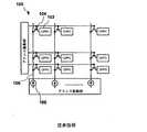
図1に、アクティブマトリクス有機発光ダイオード(AMOLED)の一般的な配列構造を示す。ディスプレイ100は、行方向と列方向に配列された画素配列102を含む。画素102は、選択トランジスタ104を介してデータ線106に接続されている。トランジスタ104は、薄膜トランジスタ(TFT)である。データ線106は、電流源108によって駆動される。データ線106に接続されたトランジスタ104のオーバーラップ容量とデータ線106自体の配線容量により、高い寄生容量が生じる。 FIG. 1 shows a general arrangement structure of an active matrix organic light emitting diode (AMOLED). The
任意の画素102における基本的なOLEDの構造では、透明陽極と金属陰極の間に薄い有機層が含まれる。有機層には、正孔注入層、正孔輸送層、発光層、および電子輸送層が含まれる。この構造に適切な電圧が印加されると、注入された正および負の電荷は発光層において結合し、光を発生させる。このように、OLEDは自発光型ディスプレイであるので、LCDのようにバックライトを必要としない。さらに電荷結合プロセスは、ほとんど遅延を生じさせないので、早い応答時間を提供できる。 The basic OLED structure in any
OLEDディスプレイは、電流制御方式のディスプレイ装置である。一方、LCDは、電圧制御方式である。OLEDは、電流プログラム方式により、薄膜トランジスタ(TFT)またはOLED自体を含むほかの構成要素の特性から電流を独立させ、電圧(Vt)変化、空間的不整合、およびOLEDの劣化を補正する。しかしながら、配線および配線に接続されたトランジスタにより生じる寄生容量は、安定時間を長くさせる。安定時間は、初期線間電圧と駆動TFTの閾値電圧の関数である。安定時間は、プリチャージにより部分的には改善できるが、この改善は、中型や大型のディスプレイには十分ではない。 The OLED display is a current-controlled display device. On the other hand, the LCD is a voltage control system. OLEDs use current programming to make currents independent of the characteristics of thin film transistors (TFTs) or other components, including the OLED itself, and correct for voltage (Vt) variations, spatial mismatch, and OLED degradation. However, the parasitic capacitance generated by the wiring and the transistor connected to the wiring lengthens the stabilization time. The stabilization time is a function of the initial line voltage and the threshold voltage of the driving TFT. The stabilization time can be partially improved by precharging, but this improvement is not sufficient for medium and large displays.
図2に、駆動トランジスタと駆動トランジスタが接続されるデータ線の寄生容量を概略的に示す。図2では、特にプログラムサイクル中における、電流源203およびトランジスタ204を含む、電流プログラム方式の画素202の等価回路を概略的に示す。容量CP210および抵抗Rp208は、寄生構成要素であり、一方、容量CS206は、蓄積コンデンサの容量である。CS206<<CP210であり、かつ、RP208が小さい場合、図2に示す回路のタイミング定数、つまり安定時間は、以下のようになる。FIG. 2 schematically shows the parasitic capacitance of the data line to which the driving transistor and the driving transistor are connected. FIG. 2 schematically shows an equivalent circuit of a current-programmed

ここでβは、Ids=β(Vgs−Vth)2で示されるトランジスタ204の電流電圧(I−V)特性の係数である。Idsはドレイン‐ソース間電流、Vgsはゲート‐ソース間電圧、Vthは閾値電圧を示す。Here, β is a coefficient of the current-voltage (IV) characteristic of the
容量CP210が40pf程度の大きな容量であり、かつ、アモルファスシリコン(a‐Si)により形成されたトランジスタ204においてβが小さい場合、τは、ミリ秒単位程度である。しかしながら、プログラムサイクルにおけるタイミングバジェットは、大型ディスプレイでは100μs以下である。OLEDの効率は改善されているので、最大輝度を得るために必要とされる電流は非常に小さいため、電流の関数であるτも格段に増大する。When the
このように、電流プログラム方式の画素の安定時間は寄生容量によって長くなり、プログラムサイクルのタイミングバジェットを制限することになる。これにより、完全に安定せず、重大なエラーを生じることにもなる。このようなエラーを回避するために、OLEDディスプレイに適した、電流プログラム方式画素の駆動における単純かつ迅速な解決策が必要とされている。 As described above, the stabilization time of the current-programmed pixel becomes longer due to the parasitic capacitance, which limits the timing budget of the program cycle. This is not completely stable and can lead to serious errors. In order to avoid such errors, there is a need for a simple and quick solution in driving current programmed pixels that is suitable for OLED displays.
リブシュ(Libsch)らによる米国特許公開公報第20040095297号は、プログラム電流を電流センサによって制御するプログラム方法を記述している。図3に、上記リブシュらによる公報の図1に示された回路の概略図を示す。プログラムサイクル中は、電流センサ302は、抵抗R304とフィードバック308の間の電圧を監視する。電流センサ302は、プログラミング電流を制御する。画素が安定すると、抵抗R304とOLED306の間を流れる電流は、所望の電流となる。フィードバック308の使用により、この駆動方法では安定時間が早い。しかしながらこの回路では、抵抗R304により消費電力が高いという欠点がある。また、この回路では、低電流も正確に検知する必要があるため、抵抗R304は、かなり大型となるため、抵抗R304の消費電力は高くなる。さらに、この回路には、不整合という別の欠点もある。空間的な不整合により抵抗R304の値が変わり、ディスプレイが不均一となる。また、回路には付加的フィードバック308もある。 US Patent Publication No. 20040095297 by Libsch et al. Describes a programming method in which program current is controlled by a current sensor. FIG. 3 shows a schematic diagram of the circuit shown in FIG. 1 of the above publication by Ribsch et al. During the program cycle,
ブー(Bu)による米国特許第6,433,488号明細書は、フィードバックループ内に電流比較器を実装するOLED駆動回路を開示している。図4に、上記ブーによる明細書の図2に示される回路の概略を示す。プログラムサイクル中は、走査信号(SCAN)は高いので、トランジスタT2 402はオフ、トランジスタT4 404はオンとなる。このため電流は、トランジスタT3 406、OLED408、およびトランジスタT1 410を流れる。電流比較器412は、フィードバック線416を介する画素電流と基準電流418の比較に基づき基準電圧414を確定する。画素が安定した後は、画素電流416は、基準電流418と一致する。この回路は、フィードバックを使用するので、画素の安定時間が早い。しかしながら、駆動サイクル中の電流経路内に2つのトランジスタ(T1 410およびT2 402)があるため、この回路の消費電力は高い。また、この方法では、4つのトランジスタと付加的フィードバック線416を使用する。 U.S. Pat. No. 6,433,488 to Bu discloses an OLED drive circuit that implements a current comparator in a feedback loop. FIG. 4 shows an outline of the circuit shown in FIG. During the program cycle, the scan signal (SCAN) is high, so
このため、周知の回路における高い消費電力を必要とせず、電流駆動回路の安定時間を改善する回路が必要である。 Therefore, there is a need for a circuit that does not require high power consumption in a known circuit and improves the stabilization time of the current drive circuit.
本発明は、OLED画素を駆動する回路に関する。本発明は、特に、安定時間を改善し、大型ディスプレイでの電流プログラム方式画素回路の使用を可能にする回路に関する。 The present invention relates to a circuit for driving an OLED pixel. The present invention particularly relates to a circuit that improves the stabilization time and enables the use of current programmed pixel circuits in large displays.
本発明の目的は、従来技術における時間に対する反応性を改善するように、回路の少なくとも1つの欠点を排除する、または、軽減することである。 The object of the present invention is to eliminate or reduce at least one drawback of the circuit so as to improve the responsiveness to time in the prior art.
本発明の1つの態様では、関連付けられた寄生容量を有し、電流プログラム方式である負荷用の負荷駆動回路を提供する。駆動回路は、負荷を制御する電圧を有するデータ線と、データ線の電圧を監視するローパスフィルタと、データ線に電流を供給する電流源とを含み、電流源は信号線とローパスフィルタからの出力とによって制御される。 One aspect of the invention provides a load drive circuit for a load that has an associated parasitic capacitance and is current programmed. The drive circuit includes a data line having a voltage for controlling a load, a low-pass filter for monitoring the voltage of the data line, and a current source for supplying a current to the data line. The current source is an output from the signal line and the low-pass filter. And controlled by.
本発明の他の態様では、寄生容量を有し、電流プログラム方式である発光ダイオード用の駆動回路を提供する。駆動回路は、発光ダイオードを制御するデータ線と、データ線の電圧を監視するローパスフィルタと、データ線に電流を供給する電流源とを含み、電流源は信号線とローパスフィルタからの出力とによって制御される。 In another aspect of the present invention, a driving circuit for a light emitting diode having parasitic capacitance and current programming is provided. The drive circuit includes a data line that controls the light emitting diode, a low-pass filter that monitors the voltage of the data line, and a current source that supplies current to the data line. The current source is based on the signal line and the output from the low-pass filter. Be controlled.
本発明のさらに他の態様では、寄生容量を有し、電流プログラム方式である発光ダイオード用の駆動回路を提供する。駆動回路は、発光ダイオードを制御するデータ線と、フィードバックループであって、アナログ‐デジタル変換器と、フィードバックループにローパスフィルタ機能を与えるアルゴリズムを実行する制御器とを含むフィードバックループと、データ線に電流を供給する電流源とを含み、電流源は、制御器から入力を受けるデジタル‐アナログ変換器からの入力を受ける。 According to still another aspect of the present invention, a driving circuit for a light emitting diode having a parasitic capacitance and having a current programming method is provided. The driving circuit includes a data line for controlling the light emitting diode, a feedback loop including an analog-to-digital converter, and a controller for executing an algorithm for providing a low-pass filter function to the feedback loop; A current source for supplying current, the current source receiving input from a digital-to-analog converter that receives input from the controller.
本発明のさらに他の態様では、ディスプレイに使用される発光ダイオードを駆動する方法であって、発光ダイオードは、寄生容量を有し、電流プログラム方式である方法を提供する。この方法は、電流源から供給される電流を発光ダイオードに供給するステップと、ローパスフィルタを含む発光ダイオードに電流を供給するデータ線の電圧を監視するステップと、電圧とデータ線の信号を複合し入力を形成して、入力を電流源に供給するステップとを含む。 In yet another aspect of the present invention, there is provided a method of driving a light emitting diode used in a display, wherein the light emitting diode has a parasitic capacitance and is a current programming method. In this method, a current supplied from a current source is supplied to a light emitting diode, a voltage of a data line supplying current to the light emitting diode including a low pass filter is monitored, and the voltage and the data line signal are combined. Forming an input and providing the input to a current source.
この発明の開示は、必ずしも本発明のすべての特徴を示すものではない。 This disclosure of the invention does not necessarily indicate all features of the invention.
本発明の上記およびその他の特徴を図面を参照しながら以下に説明し、より明白にする。 These and other features of the present invention will be described and made more apparent below with reference to the drawings.
図2に関する説明において要点を示したとおり、寄生容量が原因で、電流の安定時間は許容されたよりも長くなる。本発明の実施形態では電流源へ正のフィードバックを供給するフィードバック回路の使用が考察されている。このフィードバックにより、電流の安定時間は改善され、電流駆動方式のディスプレイに必要な応答時間を確保することができる。 As indicated in the description of FIG. 2, due to the parasitic capacitance, the current stabilization time is longer than allowed. Embodiments of the present invention contemplate use of a feedback circuit that provides positive feedback to the current source. By this feedback, the current stabilization time is improved, and the response time required for the current-driven display can be secured.
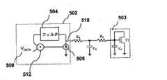
図5に、本発明の一実施形態に係る基本的なフィードバック回路を示す。ディスプレイ駆動回路502は、発光画素503を駆動する。駆動回路502は、電圧制御電流源(VCCS)506とフィードバックループとを含む。フィードバックループ内には、フィルタ504と電圧加算器512とが含まれる。電流源506は、VDATA508と、フィルタ504の出力とによって制御され、データ線510の電圧を監視する。電流源506と、フィルタ504と、電圧加算器512はディスプレイ駆動部502の一部であって、ディスプレイ駆動部502は、CMOS技術によって別のチップとして実装することも、または、ディスプレイのTFT技術によってディスプレイの一部とすることもできる。FIG. 5 shows a basic feedback circuit according to an embodiment of the present invention. The
本発明の他の実施形態では、図6に示すように、微分器602としてフィルタを実装する。寄生容量RP604が十分に小さく、かつ、VCCS606が直流電流源である場合、図6に示す回路のタイミング定数は、次の式で表すことができる。In another embodiment of the present invention, a filter is implemented as the
ここで、「i」は、VDATA608における電流を示す。Kは、微分器602の係数であって、所望の結果を得るためには寄生容量CP610に近い値を選ぶ必要がある。しかしながら、KとCPとの差が妥当な範囲内であれば、安定時間に重大な影響を及ぼすことはない。Here, “i” indicates a current in
図6に示す回路は、寄生容量610の影響を排除することができるため、電流プログラム方式の画素612に対する高速プログラムとして使用することができる。この回路は、電流プログラム方式の画素の機能を示す一般的な回路図である。図6の回路がいかなる電流プログラム方式の画素回路にも使用できることは、当業者には明白であろう。 The circuit shown in FIG. 6 can eliminate the influence of the
図7に、現在のところ好適な実施形態に係るフィルタ回路を示す。この実施形態では、ディスプレイ駆動回路702は、バンドパス(BP)フィルタ704をフィードバック機能として使用する。駆動回路702は、画素703を駆動し、正のフィードバックを使用して、寄生容量CP706の影響を管理する。プログラムサイクルの最初には、配線708の電圧は急激に変化するので、VCCS710は電流線708により多くの電流を供給する。電流線708の電圧が安定すると、電流源710により供給される電流はプログラム電流となる。また、バンドパスフィルタ704は、電流線708の高周波ノイズを軽減する。この軽減がなければ、このノイズにより電流源710の出力電流は影響を受けることになる。FIG. 7 shows a filter circuit according to a presently preferred embodiment. In this embodiment, the
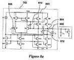
図8aに、ディスプレイ駆動回路702に使用されるバンドパスフィルタの詳細をさらに示す。約100μmの画素ピッチ内に収まるように、単純なフィルタ回路が使用されている。図8aのバンドパスフィルタは、大まかに803で示され、単極ローパスバターワースフィルタおよび微分器として実装される。図8aの回路において、駆動部は第2世代電流コンベア(CCII)を使用して実現される。Z端子808は、Y端子806に直接接続される。このため、ノードX804の電圧は、Y端子806とX端子804の間のフィードバックによって、Z端子808の電圧に従う。また、容量CLP810は、ローパスフィルタとして機能し、高周波ノイズを軽減する。一方、容量CF812は、配線の電圧に相当するX端子804における電圧を微分し、電流に変換する。電流ミラーは、この電流を複製し、プログラム電流に加算する。FIG. 8 a further shows details of the bandpass filter used in the
図8bに、デジタル実装によるローパスフィルタの他の実装を示す。図8bでは、駆動回路819は、画素825を駆動する。配線820の電圧は、アナログ‐デジタル変換器(ADC)822によって変換される。制御器824ブロックは、アルゴリズムを実行し、電流源826の電流をデジタル‐アナログ変換器(DAC)828によって変更する。制御器824が実行するアルゴリズムの重要な側面は、電流サンプルV[n]と前のサンプル[n−1]の差を算出することである。この差を考慮することによってアルゴリズムは、電流源826から供給される電流を調節し、プログラミングを高速化できる。 FIG. 8b shows another implementation of a low pass filter with a digital implementation. In FIG. 8 b, the
図8aの回路に関する安定時間の解析を図9に示す。新規電流源の特性の調査には、MATLABTMモデルが使用されている。解析を単純化するため、LPフィルタのカットオフ周波数は高いものとする。T1オーバードライブ電圧は、以下の式に表すことができる。An analysis of the stabilization time for the circuit of FIG. 8a is shown in FIG. The investigation of the characteristics of the new current source, MATLABTM model is used. In order to simplify the analysis, the cutoff frequency of the LP filter is assumed to be high. The T1 overdrive voltage can be expressed by the following equation.
ここで、VはT1のオーバードライブ電圧、CFは微分器のゲインを示す。CFは寄生容量を補償できることは明白である。Here, V is the overdrive voltage of T1, the CF indicates the gain of the differentiator. Clearly, CF can compensate for parasitic capacitance.
図9において、LPフィルタを実装する電流源702の安定時間は、40μs以下である。これに対し、従来の場合では400μsであるので、電流はフィードバックなしで電流源から供給される。さらに、ローパスフィルタのカットオフ周波数を上げることにより、電流線のノイズに対して駆動部はより敏感になることも明白である。しかしながら、カットオフ周波数を増加させることにより、速度は増す。 In FIG. 9, the stabilization time of the
図10aに、微分器またはハイパスフィルタを使用する場合における、プログラミングサイクル中の時間に対する画素電流をグラフに示す。配線ノイズは、微分器を通して電流に戻される。これにより、ノイズは増幅される。さらに、微分器は高周波信号に非常に敏感なため、駆動部を不安定にさせる。このグラフから明らかなように、配線ノイズは増幅され、信号を破壊する。図10bに、ローパスフィルタを使用する場合におけるプログラミングサイクル中の時間に対する画素電流をグラフに示す。図10bと図10aを比べると、ノイズの軽減は明らかである。 FIG. 10a graphically illustrates pixel current versus time during a programming cycle when using a differentiator or high pass filter. Wiring noise is returned to the current through the differentiator. Thereby, noise is amplified. Furthermore, the differentiator is very sensitive to high frequency signals, which makes the drive part unstable. As is apparent from this graph, the wiring noise is amplified and the signal is destroyed. FIG. 10b shows a graph of pixel current versus time during a programming cycle when using a low pass filter. Comparing FIG. 10b and FIG. 10a, the noise reduction is clear.
以上、1つまたは複数の実施形態に関連させて、本発明を説明した。しかしながら、請求項に定義された本発明の範囲を逸脱することなく、さまざまな変更および修正が可能であることは、当業者には明白であろう。 The present invention has been described above with reference to one or more embodiments. However, it will be apparent to those skilled in the art that various modifications and variations can be made without departing from the scope of the invention as defined in the claims.
Claims (17)
Translated fromJapanese前記負荷を制御する電圧を有するデータ線と、
ローパスフィルタを有し、前記データ線の電圧を監視するフィードバックループと、
前記データ線に電流を供給する電流源と、
を有し、
前記電流源は、信号線と前記ローパスフィルタからの出力とによって制御されることを特徴とする駆動回路。A current programmed load drive circuit for a load having an associated parasitic capacitance, the drive circuit comprising:
A data line having a voltage to control the load;
A feedback loop having a low-pass filter and monitoring the voltage of the data line;
A current source for supplying current to the data line;
Have
The drive circuit, wherein the current source is controlled by a signal line and an output from the low-pass filter.
前記発光ダイオードを制御するデータ線と、
前記データ線の電圧を監視するローパスフィルタと、
前記データ線に電流を供給する電流源と、
を有し、
前記電流源は、信号線と前記ローパスフィルタからの出力とによって制御されることを特徴とする駆動回路。A drive circuit for a light-emitting diode having a parasitic capacitance and current programmed, the drive circuit comprising:
A data line for controlling the light emitting diode;
A low-pass filter for monitoring the voltage of the data line;
A current source for supplying current to the data line;
Have
The drive circuit, wherein the current source is controlled by a signal line and an output from the low-pass filter.
前記発光ダイオードを制御するデータ線と、
フィードバックループであって、アナログ‐デジタル変換器と、前記フィードバックループに対しローパスフィルタの機能を与えるアルゴリズムを実行する制御器とを含むフィードバックループと、
前記データ線に電流を供給する電流源と、
を有し、
前記電流源は、前記制御器から入力を受けるディジタル‐アナログ変換器からの入力を受けることを特徴とする駆動回路。A drive circuit for a light-emitting diode having a parasitic capacitance and current programmed, the drive circuit comprising:
A data line for controlling the light emitting diode;
A feedback loop comprising an analog-to-digital converter and a controller that executes an algorithm that provides a low-pass filter function for the feedback loop;
A current source for supplying current to the data line;
Have
The drive circuit, wherein the current source receives an input from a digital-analog converter that receives an input from the controller.
前記発光ダイオードに電流を供給するステップであって、前記電流は電流源から供給されるステップと、
ローパスフィルタを含む前記発光ダイオードに前記電流を供給するデータ線の電圧を監視するステップと、
入力を形成するように、前記電圧とデータ線信号を混合するステップと、
前記電流源に前記入力を供給するステップと、
を含むことを特徴とする方法。A method of driving a light emitting diode in a display, wherein the light emitting diode has a parasitic capacitance and is a current programmed diode, the method comprising:
Supplying a current to the light emitting diode, wherein the current is supplied from a current source;
Monitoring a voltage of a data line supplying the current to the light emitting diode including a low pass filter;
Mixing the voltage and data line signal to form an input; and
Providing the input to the current source;
A method comprising the steps of:
Applications Claiming Priority (3)
| Application Number | Priority Date | Filing Date | Title |
|---|---|---|---|
| CA002496642ACA2496642A1 (en) | 2005-02-10 | 2005-02-10 | Fast settling time driving method for organic light-emitting diode (oled) displays based on current programming |
| CA2,496,642 | 2005-02-10 | ||
| PCT/CA2006/000177WO2006084360A1 (en) | 2005-02-10 | 2006-02-09 | Driving circuit for current programmed organic light-emitting diode displays |
Publications (2)
| Publication Number | Publication Date |
|---|---|
| JP2008530599Atrue JP2008530599A (en) | 2008-08-07 |
| JP5011130B2 JP5011130B2 (en) | 2012-08-29 |
Family
ID=36791467
Family Applications (1)
| Application Number | Title | Priority Date | Filing Date |
|---|---|---|---|
| JP2007554402AExpired - Fee RelatedJP5011130B2 (en) | 2005-02-10 | 2006-02-09 | Driving circuit, display and method for improving settling time of program current |
Country Status (8)
| Country | Link |
|---|---|
| US (1) | US10078984B2 (en) |
| EP (1) | EP1854338B1 (en) |
| JP (1) | JP5011130B2 (en) |
| KR (1) | KR20070102614A (en) |
| CN (1) | CN101164377B (en) |
| CA (1) | CA2496642A1 (en) |
| TW (1) | TWI409750B (en) |
| WO (1) | WO2006084360A1 (en) |
Cited By (4)
| Publication number | Priority date | Publication date | Assignee | Title |
|---|---|---|---|---|
| JP2010096990A (en)* | 2008-10-16 | 2010-04-30 | Eastman Kodak Co | Display |
| WO2010131397A1 (en)* | 2009-05-13 | 2010-11-18 | シャープ株式会社 | Display apparatus |
| JP2012500407A (en)* | 2008-08-15 | 2012-01-05 | ケンブリッジ ディスプレイ テクノロジー リミテッド | Active matrix display device |
| JP2013539551A (en)* | 2010-08-30 | 2013-10-24 | グレンツェバッハ・マシーネンバウ・ゲーエムベーハー | Device and method for operating a flight simulator with special feeling |
Families Citing this family (79)
| Publication number | Priority date | Publication date | Assignee | Title |
|---|---|---|---|---|
| CA2443206A1 (en) | 2003-09-23 | 2005-03-23 | Ignis Innovation Inc. | Amoled display backplanes - pixel driver circuits, array architecture, and external compensation |
| CA2472671A1 (en) | 2004-06-29 | 2005-12-29 | Ignis Innovation Inc. | Voltage-programming scheme for current-driven amoled displays |
| US9171500B2 (en) | 2011-05-20 | 2015-10-27 | Ignis Innovation Inc. | System and methods for extraction of parasitic parameters in AMOLED displays |
| US10012678B2 (en) | 2004-12-15 | 2018-07-03 | Ignis Innovation Inc. | Method and system for programming, calibrating and/or compensating, and driving an LED display |
| US9799246B2 (en) | 2011-05-20 | 2017-10-24 | Ignis Innovation Inc. | System and methods for extraction of threshold and mobility parameters in AMOLED displays |
| US8576217B2 (en) | 2011-05-20 | 2013-11-05 | Ignis Innovation Inc. | System and methods for extraction of threshold and mobility parameters in AMOLED displays |
| TWI402790B (en) | 2004-12-15 | 2013-07-21 | Ignis Innovation Inc | Method and system for programming, calibrating and driving a light-emitting element display |
| US20140111567A1 (en) | 2005-04-12 | 2014-04-24 | Ignis Innovation Inc. | System and method for compensation of non-uniformities in light emitting device displays |
| US10013907B2 (en) | 2004-12-15 | 2018-07-03 | Ignis Innovation Inc. | Method and system for programming, calibrating and/or compensating, and driving an LED display |
| US9275579B2 (en) | 2004-12-15 | 2016-03-01 | Ignis Innovation Inc. | System and methods for extraction of threshold and mobility parameters in AMOLED displays |
| US9280933B2 (en) | 2004-12-15 | 2016-03-08 | Ignis Innovation Inc. | System and methods for extraction of threshold and mobility parameters in AMOLED displays |
| CA2496642A1 (en)* | 2005-02-10 | 2006-08-10 | Ignis Innovation Inc. | Fast settling time driving method for organic light-emitting diode (oled) displays based on current programming |
| JP5355080B2 (en) | 2005-06-08 | 2013-11-27 | イグニス・イノベイション・インコーポレーテッド | Method and system for driving a light emitting device display |
| CA2518276A1 (en) | 2005-09-13 | 2007-03-13 | Ignis Innovation Inc. | Compensation technique for luminance degradation in electro-luminance devices |
| TW200746022A (en) | 2006-04-19 | 2007-12-16 | Ignis Innovation Inc | Stable driving scheme for active matrix displays |
| JP5226248B2 (en)* | 2006-08-02 | 2013-07-03 | ルネサスエレクトロニクス株式会社 | Temperature detection circuit and semiconductor device |
| CA2556961A1 (en) | 2006-08-15 | 2008-02-15 | Ignis Innovation Inc. | Oled compensation technique based on oled capacitance |
| WO2009035588A1 (en)* | 2007-09-12 | 2009-03-19 | Corning Incorporated | Derivative sampled, fast settling time current driver |
| JP2009128756A (en)* | 2007-11-27 | 2009-06-11 | Oki Semiconductor Co Ltd | Current driver device |
| CA2688870A1 (en) | 2009-11-30 | 2011-05-30 | Ignis Innovation Inc. | Methode and techniques for improving display uniformity |
| US10319307B2 (en) | 2009-06-16 | 2019-06-11 | Ignis Innovation Inc. | Display system with compensation techniques and/or shared level resources |
| US9384698B2 (en) | 2009-11-30 | 2016-07-05 | Ignis Innovation Inc. | System and methods for aging compensation in AMOLED displays |
| CA2669367A1 (en) | 2009-06-16 | 2010-12-16 | Ignis Innovation Inc | Compensation technique for color shift in displays |
| US9311859B2 (en) | 2009-11-30 | 2016-04-12 | Ignis Innovation Inc. | Resetting cycle for aging compensation in AMOLED displays |
| US20110109614A1 (en)* | 2009-11-12 | 2011-05-12 | Silicon Touch Technology Inc. | Driving circuit and method of light emitting diode |
| US10996258B2 (en) | 2009-11-30 | 2021-05-04 | Ignis Innovation Inc. | Defect detection and correction of pixel circuits for AMOLED displays |
| US8803417B2 (en) | 2009-12-01 | 2014-08-12 | Ignis Innovation Inc. | High resolution pixel architecture |
| CA2687631A1 (en) | 2009-12-06 | 2011-06-06 | Ignis Innovation Inc | Low power driving scheme for display applications |
| US10089921B2 (en) | 2010-02-04 | 2018-10-02 | Ignis Innovation Inc. | System and methods for extracting correlation curves for an organic light emitting device |
| US10163401B2 (en) | 2010-02-04 | 2018-12-25 | Ignis Innovation Inc. | System and methods for extracting correlation curves for an organic light emitting device |
| US9881532B2 (en) | 2010-02-04 | 2018-01-30 | Ignis Innovation Inc. | System and method for extracting correlation curves for an organic light emitting device |
| US20140313111A1 (en) | 2010-02-04 | 2014-10-23 | Ignis Innovation Inc. | System and methods for extracting correlation curves for an organic light emitting device |
| CA2692097A1 (en) | 2010-02-04 | 2011-08-04 | Ignis Innovation Inc. | Extracting correlation curves for light emitting device |
| US10176736B2 (en)* | 2010-02-04 | 2019-01-08 | Ignis Innovation Inc. | System and methods for extracting correlation curves for an organic light emitting device |
| CA2696778A1 (en) | 2010-03-17 | 2011-09-17 | Ignis Innovation Inc. | Lifetime, uniformity, parameter extraction methods |
| TWI505248B (en)* | 2010-11-30 | 2015-10-21 | Univ Nat Cheng Kung | Oled display and controlling method thereof |
| US8907991B2 (en) | 2010-12-02 | 2014-12-09 | Ignis Innovation Inc. | System and methods for thermal compensation in AMOLED displays |
| US9530349B2 (en) | 2011-05-20 | 2016-12-27 | Ignis Innovations Inc. | Charged-based compensation and parameter extraction in AMOLED displays |
| US9466240B2 (en) | 2011-05-26 | 2016-10-11 | Ignis Innovation Inc. | Adaptive feedback system for compensating for aging pixel areas with enhanced estimation speed |
| US9773439B2 (en) | 2011-05-27 | 2017-09-26 | Ignis Innovation Inc. | Systems and methods for aging compensation in AMOLED displays |
| US9324268B2 (en) | 2013-03-15 | 2016-04-26 | Ignis Innovation Inc. | Amoled displays with multiple readout circuits |
| US10089924B2 (en) | 2011-11-29 | 2018-10-02 | Ignis Innovation Inc. | Structural and low-frequency non-uniformity compensation |
| US8937632B2 (en) | 2012-02-03 | 2015-01-20 | Ignis Innovation Inc. | Driving system for active-matrix displays |
| US9747834B2 (en) | 2012-05-11 | 2017-08-29 | Ignis Innovation Inc. | Pixel circuits including feedback capacitors and reset capacitors, and display systems therefore |
| US8922544B2 (en) | 2012-05-23 | 2014-12-30 | Ignis Innovation Inc. | Display systems with compensation for line propagation delay |
| US9336717B2 (en) | 2012-12-11 | 2016-05-10 | Ignis Innovation Inc. | Pixel circuits for AMOLED displays |
| US9786223B2 (en) | 2012-12-11 | 2017-10-10 | Ignis Innovation Inc. | Pixel circuits for AMOLED displays |
| CN108665836B (en) | 2013-01-14 | 2021-09-03 | 伊格尼斯创新公司 | Method and system for compensating for deviations of a measured device current from a reference current |
| US9830857B2 (en) | 2013-01-14 | 2017-11-28 | Ignis Innovation Inc. | Cleaning common unwanted signals from pixel measurements in emissive displays |
| EP3043338A1 (en) | 2013-03-14 | 2016-07-13 | Ignis Innovation Inc. | Re-interpolation with edge detection for extracting an aging pattern for amoled displays |
| WO2014174427A1 (en) | 2013-04-22 | 2014-10-30 | Ignis Innovation Inc. | Inspection system for oled display panels |
| CN105474296B (en) | 2013-08-12 | 2017-08-18 | 伊格尼斯创新公司 | A method and device for driving a display using image data |
| US9741282B2 (en) | 2013-12-06 | 2017-08-22 | Ignis Innovation Inc. | OLED display system and method |
| US9761170B2 (en)* | 2013-12-06 | 2017-09-12 | Ignis Innovation Inc. | Correction for localized phenomena in an image array |
| US9502653B2 (en) | 2013-12-25 | 2016-11-22 | Ignis Innovation Inc. | Electrode contacts |
| DE102015206281A1 (en) | 2014-04-08 | 2015-10-08 | Ignis Innovation Inc. | Display system with shared level resources for portable devices |
| US9378686B2 (en) | 2014-05-01 | 2016-06-28 | Pixtronix, Inc. | Display circuit incorporating data feedback loop |
| CN104050918B (en)* | 2014-06-16 | 2016-02-03 | 上海和辉光电有限公司 | Pixel unit drive circuit and display device |
| CA2879462A1 (en) | 2015-01-23 | 2016-07-23 | Ignis Innovation Inc. | Compensation for color variation in emissive devices |
| CA2889870A1 (en) | 2015-05-04 | 2016-11-04 | Ignis Innovation Inc. | Optical feedback system |
| CA2892714A1 (en) | 2015-05-27 | 2016-11-27 | Ignis Innovation Inc | Memory bandwidth reduction in compensation system |
| CA2900170A1 (en) | 2015-08-07 | 2017-02-07 | Gholamreza Chaji | Calibration of pixel based on improved reference values |
| US11030942B2 (en) | 2017-10-13 | 2021-06-08 | Jasper Display Corporation | Backplane adaptable to drive emissive pixel arrays of differing pitches |
| US10951875B2 (en) | 2018-07-03 | 2021-03-16 | Raxium, Inc. | Display processing circuitry |
| US11238792B2 (en)* | 2018-07-10 | 2022-02-01 | Seeya Optronics Co., Ltd. | Pixel circuit and display device |
| US10636357B1 (en)* | 2018-12-10 | 2020-04-28 | Sharp Kabushiki Kaisha | Analogue external compensation system for TFT pixel OLED circuit |
| US11710445B2 (en) | 2019-01-24 | 2023-07-25 | Google Llc | Backplane configurations and operations |
| US11637219B2 (en) | 2019-04-12 | 2023-04-25 | Google Llc | Monolithic integration of different light emitting structures on a same substrate |
| US11250777B2 (en)* | 2019-06-28 | 2022-02-15 | Jasper Display Corp. | Backplane for an array of emissive elements |
| US11238782B2 (en) | 2019-06-28 | 2022-02-01 | Jasper Display Corp. | Backplane for an array of emissive elements |
| US11626062B2 (en) | 2020-02-18 | 2023-04-11 | Google Llc | System and method for modulating an array of emissive elements |
| KR102785804B1 (en) | 2020-04-06 | 2025-03-26 | 구글 엘엘씨 | Display Assembly |
| US11538431B2 (en) | 2020-06-29 | 2022-12-27 | Google Llc | Larger backplane suitable for high speed applications |
| CN111883063B (en)* | 2020-07-17 | 2021-11-12 | 合肥维信诺科技有限公司 | Pixel circuit, display panel and display device |
| US11164494B1 (en) | 2020-10-30 | 2021-11-02 | Innolux Corporation | Pixel circuit, display device and detecting method |
| CN114527817B (en)* | 2020-11-23 | 2025-06-10 | 意法半导体(鲁塞)公司 | Smart Card |
| US12244786B2 (en) | 2020-12-21 | 2025-03-04 | Google Llc | High density pixel arrays for auto-viewed 3D displays |
| CN113299235B (en)* | 2021-05-20 | 2022-10-25 | 京东方科技集团股份有限公司 | Pixel circuit, driving method thereof and display device |
| TW202303555A (en) | 2021-07-14 | 2023-01-16 | 美商谷歌有限責任公司 | Backplane and method for pulse width modulation |
Citations (4)
| Publication number | Priority date | Publication date | Assignee | Title |
|---|---|---|---|---|
| JPH01272298A (en)* | 1988-04-25 | 1989-10-31 | Yamaha Corp | Driving device |
| JP2002055654A (en)* | 2000-08-10 | 2002-02-20 | Nec Corp | Electroluminescence display |
| JP2002514320A (en)* | 1997-04-23 | 2002-05-14 | サーノフ コーポレイション | Active matrix light emitting diode pixel structure and method |
| JP2003124519A (en)* | 2001-10-11 | 2003-04-25 | Sharp Corp | Light emitting diode drive circuit and optical transmission device using the same |
Family Cites Families (432)
| Publication number | Priority date | Publication date | Assignee | Title |
|---|---|---|---|---|
| US3506851A (en) | 1966-12-14 | 1970-04-14 | North American Rockwell | Field effect transistor driver using capacitor feedback |
| US3774055A (en) | 1972-01-24 | 1973-11-20 | Nat Semiconductor Corp | Clocked bootstrap inverter circuit |
| JPS52119160A (en) | 1976-03-31 | 1977-10-06 | Nec Corp | Semiconductor circuit with insulating gate type field dffect transisto r |
| US4160934A (en) | 1977-08-11 | 1979-07-10 | Bell Telephone Laboratories, Incorporated | Current control circuit for light emitting diode |
| US4354162A (en) | 1981-02-09 | 1982-10-12 | National Semiconductor Corporation | Wide dynamic range control amplifier with offset correction |
| JPS60218626A (en) | 1984-04-13 | 1985-11-01 | Sharp Corp | Color llquid crystal display device |
| JPS61161093A (en) | 1985-01-09 | 1986-07-21 | Sony Corp | Dynamic uniformity correction device |
| US4617555A (en)* | 1985-04-17 | 1986-10-14 | Data Distribution Devices, Inc. | Receiver for audible alarm |
| DE68925434T2 (en)* | 1988-04-25 | 1996-11-14 | Yamaha Corp | Electroacoustic drive circuit |
| US4996523A (en) | 1988-10-20 | 1991-02-26 | Eastman Kodak Company | Electroluminescent storage display with improved intensity driver circuits |
| US5198803A (en)* | 1990-06-06 | 1993-03-30 | Opto Tech Corporation | Large scale movie display system with multiple gray levels |
| JP3039791B2 (en) | 1990-06-08 | 2000-05-08 | 富士通株式会社 | DA converter |
| EP0462333B1 (en) | 1990-06-11 | 1994-08-31 | International Business Machines Corporation | Display system |
| JPH04158570A (en) | 1990-10-22 | 1992-06-01 | Seiko Epson Corp | Structure of semiconductor device and manufacture thereof |
| US5153420A (en) | 1990-11-28 | 1992-10-06 | Xerox Corporation | Timing independent pixel-scale light sensing apparatus |
| US5204661A (en) | 1990-12-13 | 1993-04-20 | Xerox Corporation | Input/output pixel circuit and array of such circuits |
| US5280280A (en) | 1991-05-24 | 1994-01-18 | Robert Hotto | DC integrating display driver employing pixel status memories |
| US5489918A (en) | 1991-06-14 | 1996-02-06 | Rockwell International Corporation | Method and apparatus for dynamically and adjustably generating active matrix liquid crystal display gray level voltages |
| US5589847A (en) | 1991-09-23 | 1996-12-31 | Xerox Corporation | Switched capacitor analog circuits using polysilicon thin film technology |
| US5266515A (en) | 1992-03-02 | 1993-11-30 | Motorola, Inc. | Fabricating dual gate thin film transistors |
| US5572444A (en) | 1992-08-19 | 1996-11-05 | Mtl Systems, Inc. | Method and apparatus for automatic performance evaluation of electronic display devices |
| EP0693210A4 (en) | 1993-04-05 | 1996-11-20 | Cirrus Logic Inc | System for compensating crosstalk in lcds |
| JPH06314977A (en) | 1993-04-28 | 1994-11-08 | Nec Ic Microcomput Syst Ltd | Current output type d/a converter circuit |
| JPH0799321A (en) | 1993-05-27 | 1995-04-11 | Sony Corp | Method and apparatus for manufacturing thin film semiconductor element |
| JPH07120722A (en) | 1993-06-30 | 1995-05-12 | Sharp Corp | Liquid crystal display device and driving method thereof |
| JP3067949B2 (en) | 1994-06-15 | 2000-07-24 | シャープ株式会社 | Electronic device and liquid crystal display device |
| JPH0830231A (en) | 1994-07-18 | 1996-02-02 | Toshiba Corp | LED dot matrix display and dimming method thereof |
| US5714968A (en) | 1994-08-09 | 1998-02-03 | Nec Corporation | Current-dependent light-emitting element drive circuit for use in active matrix display device |
| US6476798B1 (en)* | 1994-08-22 | 2002-11-05 | International Game Technology | Reduced noise touch screen apparatus and method |
| US5498880A (en) | 1995-01-12 | 1996-03-12 | E. I. Du Pont De Nemours And Company | Image capture panel using a solid state device |
| US5745660A (en) | 1995-04-26 | 1998-04-28 | Polaroid Corporation | Image rendering system and method for generating stochastic threshold arrays for use therewith |
| US5619033A (en) | 1995-06-07 | 1997-04-08 | Xerox Corporation | Layered solid state photodiode sensor array |
| JPH08340243A (en) | 1995-06-14 | 1996-12-24 | Canon Inc | Bias circuit |
| US5748160A (en) | 1995-08-21 | 1998-05-05 | Mororola, Inc. | Active driven LED matrices |
| JP3272209B2 (en) | 1995-09-07 | 2002-04-08 | アルプス電気株式会社 | LCD drive circuit |
| JPH0990405A (en) | 1995-09-21 | 1997-04-04 | Sharp Corp | Thin film transistor |
| US5945972A (en) | 1995-11-30 | 1999-08-31 | Kabushiki Kaisha Toshiba | Display device |
| JPH09179525A (en) | 1995-12-26 | 1997-07-11 | Pioneer Electron Corp | Method and device for driving capacitive light emitting element |
| US5923794A (en) | 1996-02-06 | 1999-07-13 | Polaroid Corporation | Current-mediated active-pixel image sensing device with current reset |
| US5949398A (en) | 1996-04-12 | 1999-09-07 | Thomson Multimedia S.A. | Select line driver for a display matrix with toggling backplane |
| US6271825B1 (en) | 1996-04-23 | 2001-08-07 | Rainbow Displays, Inc. | Correction methods for brightness in electronic display |
| US5723950A (en)* | 1996-06-10 | 1998-03-03 | Motorola | Pre-charge driver for light emitting devices and method |
| JP3266177B2 (en) | 1996-09-04 | 2002-03-18 | 住友電気工業株式会社 | Current mirror circuit, reference voltage generating circuit and light emitting element driving circuit using the same |
| US5952991A (en) | 1996-11-14 | 1999-09-14 | Kabushiki Kaisha Toshiba | Liquid crystal display |
| US5874803A (en) | 1997-09-09 | 1999-02-23 | The Trustees Of Princeton University | Light emitting device with stack of OLEDS and phosphor downconverter |
| US5990629A (en) | 1997-01-28 | 1999-11-23 | Casio Computer Co., Ltd. | Electroluminescent display device and a driving method thereof |
| US5917280A (en) | 1997-02-03 | 1999-06-29 | The Trustees Of Princeton University | Stacked organic light emitting devices |
| CN100341042C (en) | 1997-02-17 | 2007-10-03 | 精工爱普生株式会社 | Display device |
| JPH10254410A (en) | 1997-03-12 | 1998-09-25 | Pioneer Electron Corp | Organic electroluminescent display device, and driving method therefor |
| US6518962B2 (en) | 1997-03-12 | 2003-02-11 | Seiko Epson Corporation | Pixel circuit display apparatus and electronic apparatus equipped with current driving type light-emitting device |
| US5903248A (en) | 1997-04-11 | 1999-05-11 | Spatialight, Inc. | Active matrix display having pixel driving circuits with integrated charge pumps |
| US5952789A (en) | 1997-04-14 | 1999-09-14 | Sarnoff Corporation | Active matrix organic light emitting diode (amoled) display pixel structure and data load/illuminate circuit therefor |
| US6229506B1 (en)* | 1997-04-23 | 2001-05-08 | Sarnoff Corporation | Active matrix light emitting diode pixel structure and concomitant method |
| US5815303A (en) | 1997-06-26 | 1998-09-29 | Xerox Corporation | Fault tolerant projective display having redundant light modulators |
| US6023259A (en) | 1997-07-11 | 2000-02-08 | Fed Corporation | OLED active matrix using a single transistor current mode pixel design |
| KR100323441B1 (en) | 1997-08-20 | 2002-06-20 | 윤종용 | Mpeg2 motion picture coding/decoding system |
| US20010043173A1 (en) | 1997-09-04 | 2001-11-22 | Ronald Roy Troutman | Field sequential gray in active matrix led display using complementary transistor pixel circuits |
| JPH1187720A (en) | 1997-09-08 | 1999-03-30 | Sanyo Electric Co Ltd | Semiconductor device and liquid crystal display device |
| US6738035B1 (en) | 1997-09-22 | 2004-05-18 | Nongqiang Fan | Active matrix LCD based on diode switches and methods of improving display uniformity of same |
| JP3767877B2 (en) | 1997-09-29 | 2006-04-19 | 三菱化学株式会社 | Active matrix light emitting diode pixel structure and method thereof |
| US6909419B2 (en) | 1997-10-31 | 2005-06-21 | Kopin Corporation | Portable microdisplay system |
| US6069365A (en) | 1997-11-25 | 2000-05-30 | Alan Y. Chow | Optical processor based imaging system |
| JP3755277B2 (en) | 1998-01-09 | 2006-03-15 | セイコーエプソン株式会社 | Electro-optical device drive circuit, electro-optical device, and electronic apparatus |
| JPH11231805A (en) | 1998-02-10 | 1999-08-27 | Sanyo Electric Co Ltd | Display device |
| US6445369B1 (en)* | 1998-02-20 | 2002-09-03 | The University Of Hong Kong | Light emitting diode dot matrix display system with audio output |
| US6259424B1 (en) | 1998-03-04 | 2001-07-10 | Victor Company Of Japan, Ltd. | Display matrix substrate, production method of the same and display matrix circuit |
| FR2775821B1 (en) | 1998-03-05 | 2000-05-26 | Jean Claude Decaux | LIGHT DISPLAY PANEL |
| US6097360A (en) | 1998-03-19 | 2000-08-01 | Holloman; Charles J | Analog driver for LED or similar display element |
| JP3252897B2 (en) | 1998-03-31 | 2002-02-04 | 日本電気株式会社 | Element driving device and method, image display device |
| JP2931975B1 (en) | 1998-05-25 | 1999-08-09 | アジアエレクトロニクス株式会社 | TFT array inspection method and device |
| JP3702096B2 (en) | 1998-06-08 | 2005-10-05 | 三洋電機株式会社 | Thin film transistor and display device |
| GB9812742D0 (en) | 1998-06-12 | 1998-08-12 | Philips Electronics Nv | Active matrix electroluminescent display devices |
| JP2000075854A (en) | 1998-06-18 | 2000-03-14 | Matsushita Electric Ind Co Ltd | Image processing device and display device using the same |
| CA2242720C (en) | 1998-07-09 | 2000-05-16 | Ibm Canada Limited-Ibm Canada Limitee | Programmable led driver |
| JP2953465B1 (en) | 1998-08-14 | 1999-09-27 | 日本電気株式会社 | Constant current drive circuit |
| JP2000081607A (en) | 1998-09-04 | 2000-03-21 | Denso Corp | Matrix type liquid crystal display device |
| US6417825B1 (en) | 1998-09-29 | 2002-07-09 | Sarnoff Corporation | Analog active matrix emissive display |
| US6501098B2 (en) | 1998-11-25 | 2002-12-31 | Semiconductor Energy Laboratory Co, Ltd. | Semiconductor device |
| JP3423232B2 (en) | 1998-11-30 | 2003-07-07 | 三洋電機株式会社 | Active EL display |
| JP3031367B1 (en) | 1998-12-02 | 2000-04-10 | 日本電気株式会社 | Image sensor |
| JP2000174282A (en) | 1998-12-03 | 2000-06-23 | Semiconductor Energy Lab Co Ltd | Semiconductor device |
| TW527579B (en) | 1998-12-14 | 2003-04-11 | Kopin Corp | Portable microdisplay system and applications |
| US6639244B1 (en) | 1999-01-11 | 2003-10-28 | Semiconductor Energy Laboratory Co., Ltd. | Semiconductor device and method of fabricating the same |
| JP3686769B2 (en) | 1999-01-29 | 2005-08-24 | 日本電気株式会社 | Organic EL element driving apparatus and driving method |
| JP2000231346A (en) | 1999-02-09 | 2000-08-22 | Sanyo Electric Co Ltd | Electroluminescence display device |
| US7122835B1 (en) | 1999-04-07 | 2006-10-17 | Semiconductor Energy Laboratory Co., Ltd. | Electrooptical device and a method of manufacturing the same |
| US7012600B2 (en) | 1999-04-30 | 2006-03-14 | E Ink Corporation | Methods for driving bistable electro-optic displays, and apparatus for use therein |
| JP4565700B2 (en) | 1999-05-12 | 2010-10-20 | ルネサスエレクトロニクス株式会社 | Semiconductor device |
| US6690344B1 (en) | 1999-05-14 | 2004-02-10 | Ngk Insulators, Ltd. | Method and apparatus for driving device and display |
| KR100296113B1 (en) | 1999-06-03 | 2001-07-12 | 구본준, 론 위라하디락사 | ElectroLuminescent Display |
| JP4092857B2 (en) | 1999-06-17 | 2008-05-28 | ソニー株式会社 | Image display device |
| US6437106B1 (en) | 1999-06-24 | 2002-08-20 | Abbott Laboratories | Process for preparing 6-o-substituted erythromycin derivatives |
| US7379039B2 (en) | 1999-07-14 | 2008-05-27 | Sony Corporation | Current drive circuit and display device using same pixel circuit, and drive method |
| EP1130565A4 (en) | 1999-07-14 | 2006-10-04 | Sony Corp | Current drive circuit and display comprising the same, pixel circuit, and drive method |
| JP2001119610A (en)* | 1999-08-10 | 2001-04-27 | Alps Electric Co Ltd | Contour detection circuit and image display device |
| EP1129446A1 (en) | 1999-09-11 | 2001-09-05 | Koninklijke Philips Electronics N.V. | Active matrix electroluminescent display device |
| GB9923261D0 (en)* | 1999-10-02 | 1999-12-08 | Koninkl Philips Electronics Nv | Active matrix electroluminescent display device |
| WO2001026085A1 (en) | 1999-10-04 | 2001-04-12 | Matsushita Electric Industrial Co., Ltd. | Method of driving display panel, and display panel luminance correction device and display panel driving device |
| EP1138036A1 (en) | 1999-10-12 | 2001-10-04 | Koninklijke Philips Electronics N.V. | Led display device |
| US6392617B1 (en) | 1999-10-27 | 2002-05-21 | Agilent Technologies, Inc. | Active matrix light emitting diode display |
| JP2001134217A (en) | 1999-11-09 | 2001-05-18 | Tdk Corp | Driving device for organic el element |
| JP2001147659A (en) | 1999-11-18 | 2001-05-29 | Sony Corp | Display device |
| TW587239B (en) | 1999-11-30 | 2004-05-11 | Semiconductor Energy Lab | Electric device |
| GB9929501D0 (en) | 1999-12-14 | 2000-02-09 | Koninkl Philips Electronics Nv | Image sensor |
| TW573165B (en) | 1999-12-24 | 2004-01-21 | Sanyo Electric Co | Display device |
| US6307322B1 (en) | 1999-12-28 | 2001-10-23 | Sarnoff Corporation | Thin-film transistor circuitry with reduced sensitivity to variance in transistor threshold voltage |
| JP2001195014A (en) | 2000-01-14 | 2001-07-19 | Tdk Corp | Driving device for organic el element |
| JP4907753B2 (en) | 2000-01-17 | 2012-04-04 | エーユー オプトロニクス コーポレイション | Liquid crystal display |
| WO2001054107A1 (en) | 2000-01-21 | 2001-07-26 | Emagin Corporation | Gray scale pixel driver for electronic display and method of operation therefor |
| US6639265B2 (en) | 2000-01-26 | 2003-10-28 | Semiconductor Energy Laboratory Co., Ltd. | Semiconductor device and method of manufacturing the semiconductor device |
| US7030921B2 (en) | 2000-02-01 | 2006-04-18 | Minolta Co., Ltd. | Solid-state image-sensing device |
| US6414661B1 (en) | 2000-02-22 | 2002-07-02 | Sarnoff Corporation | Method and apparatus for calibrating display devices and automatically compensating for loss in their efficiency over time |
| TW521226B (en) | 2000-03-27 | 2003-02-21 | Semiconductor Energy Lab | Electro-optical device |
| JP2001284592A (en) | 2000-03-29 | 2001-10-12 | Sony Corp | Thin film semiconductor device and driving method thereof |
| US6528950B2 (en) | 2000-04-06 | 2003-03-04 | Semiconductor Energy Laboratory Co., Ltd. | Electronic device and driving method |
| US7061313B2 (en)* | 2000-05-05 | 2006-06-13 | Telefonaktiebolaget Lm Ericsson (Publ) | Dual feedback linear amplifier |
| US6583576B2 (en) | 2000-05-08 | 2003-06-24 | Semiconductor Energy Laboratory Co., Ltd. | Light-emitting device, and electric device using the same |
| TW493153B (en) | 2000-05-22 | 2002-07-01 | Koninkl Philips Electronics Nv | Display device |
| EP1158483A3 (en)* | 2000-05-24 | 2003-02-05 | Eastman Kodak Company | Solid-state display with reference pixel |
| JP4703815B2 (en) | 2000-05-26 | 2011-06-15 | 株式会社半導体エネルギー研究所 | MOS type sensor driving method and imaging method |
| TW461002B (en) | 2000-06-05 | 2001-10-21 | Ind Tech Res Inst | Testing apparatus and testing method for organic light emitting diode array |
| JP4831889B2 (en) | 2000-06-22 | 2011-12-07 | 株式会社半導体エネルギー研究所 | Display device |
| US6738034B2 (en) | 2000-06-27 | 2004-05-18 | Hitachi, Ltd. | Picture image display device and method of driving the same |
| JP3877049B2 (en) | 2000-06-27 | 2007-02-07 | 株式会社日立製作所 | Image display apparatus and driving method thereof |
| JP2002032058A (en) | 2000-07-18 | 2002-01-31 | Nec Corp | Display device |
| JP3437152B2 (en) | 2000-07-28 | 2003-08-18 | ウインテスト株式会社 | Apparatus and method for evaluating organic EL display |
| JP2002049325A (en) | 2000-07-31 | 2002-02-15 | Seiko Instruments Inc | Illuminator for correcting display color temperature and flat panel display |
| US6304039B1 (en) | 2000-08-08 | 2001-10-16 | E-Lite Technologies, Inc. | Power supply for illuminating an electro-luminescent panel |
| US6828950B2 (en) | 2000-08-10 | 2004-12-07 | Semiconductor Energy Laboratory Co., Ltd. | Display device and method of driving the same |
| TW507192B (en) | 2000-09-18 | 2002-10-21 | Sanyo Electric Co | Display device |
| JP3838063B2 (en) | 2000-09-29 | 2006-10-25 | セイコーエプソン株式会社 | Driving method of organic electroluminescence device |
| JP4925528B2 (en) | 2000-09-29 | 2012-04-25 | 三洋電機株式会社 | Display device |
| US6781567B2 (en) | 2000-09-29 | 2004-08-24 | Seiko Epson Corporation | Driving method for electro-optical device, electro-optical device, and electronic apparatus |
| JP2002162934A (en) | 2000-09-29 | 2002-06-07 | Eastman Kodak Co | Flat-panel display with luminance feedback |
| US7315295B2 (en) | 2000-09-29 | 2008-01-01 | Seiko Epson Corporation | Driving method for electro-optical device, electro-optical device, and electronic apparatus |
| TW550530B (en) | 2000-10-27 | 2003-09-01 | Semiconductor Energy Lab | Display device and method of driving the same |
| JP2002141420A (en) | 2000-10-31 | 2002-05-17 | Mitsubishi Electric Corp | Semiconductor device and manufacturing method thereof |
| US6320325B1 (en) | 2000-11-06 | 2001-11-20 | Eastman Kodak Company | Emissive display with luminance feedback from a representative pixel |
| US7127380B1 (en) | 2000-11-07 | 2006-10-24 | Alliant Techsystems Inc. | System for performing coupled finite analysis |
| KR100405026B1 (en) | 2000-12-22 | 2003-11-07 | 엘지.필립스 엘시디 주식회사 | Liquid Crystal Display |
| TW561445B (en)* | 2001-01-02 | 2003-11-11 | Chi Mei Optoelectronics Corp | OLED active driving system with current feedback |
| US6580657B2 (en) | 2001-01-04 | 2003-06-17 | International Business Machines Corporation | Low-power organic light emitting diode pixel circuit |
| JP3593982B2 (en) | 2001-01-15 | 2004-11-24 | ソニー株式会社 | Active matrix type display device, active matrix type organic electroluminescence display device, and driving method thereof |
| US6323631B1 (en) | 2001-01-18 | 2001-11-27 | Sunplus Technology Co., Ltd. | Constant current driver with auto-clamped pre-charge function |
| JP2002215063A (en) | 2001-01-19 | 2002-07-31 | Sony Corp | Active matrix display |
| TW569016B (en) | 2001-01-29 | 2004-01-01 | Semiconductor Energy Lab | Light emitting device |
| CN1302313C (en) | 2001-02-05 | 2007-02-28 | 国际商业机器公司 | Liquid crystal display device |
| TWI248319B (en) | 2001-02-08 | 2006-01-21 | Semiconductor Energy Lab | Light emitting device and electronic equipment using the same |
| JP2002244617A (en) | 2001-02-15 | 2002-08-30 | Sanyo Electric Co Ltd | Organic el pixel circuit |
| US20040129933A1 (en) | 2001-02-16 | 2004-07-08 | Arokia Nathan | Pixel current driver for organic light emitting diode displays |
| WO2002067328A2 (en) | 2001-02-16 | 2002-08-29 | Ignis Innovation Inc. | Organic light emitting diode display having shield electrodes |
| CA2507276C (en) | 2001-02-16 | 2006-08-22 | Ignis Innovation Inc. | Pixel current driver for organic light emitting diode displays |
| US7569849B2 (en) | 2001-02-16 | 2009-08-04 | Ignis Innovation Inc. | Pixel driver circuit and pixel circuit having the pixel driver circuit |
| US7061451B2 (en) | 2001-02-21 | 2006-06-13 | Semiconductor Energy Laboratory Co., Ltd, | Light emitting device and electronic device |
| US6753654B2 (en) | 2001-02-21 | 2004-06-22 | Semiconductor Energy Laboratory Co., Ltd. | Light emitting device and electronic appliance |
| JP4212815B2 (en) | 2001-02-21 | 2009-01-21 | 株式会社半導体エネルギー研究所 | Light emitting device |
| US7352786B2 (en) | 2001-03-05 | 2008-04-01 | Fuji Xerox Co., Ltd. | Apparatus for driving light emitting element and system for driving light emitting element |
| JP2002278513A (en) | 2001-03-19 | 2002-09-27 | Sharp Corp | Electro-optical device |
| JPWO2002075709A1 (en) | 2001-03-21 | 2004-07-08 | キヤノン株式会社 | Driver circuit for active matrix light emitting device |
| US7164417B2 (en) | 2001-03-26 | 2007-01-16 | Eastman Kodak Company | Dynamic controller for active-matrix displays |
| JP3819723B2 (en) | 2001-03-30 | 2006-09-13 | 株式会社日立製作所 | Display device and driving method thereof |
| US7136058B2 (en) | 2001-04-27 | 2006-11-14 | Kabushiki Kaisha Toshiba | Display apparatus, digital-to-analog conversion circuit and digital-to-analog conversion method |
| JP4785271B2 (en) | 2001-04-27 | 2011-10-05 | 株式会社半導体エネルギー研究所 | Liquid crystal display device, electronic equipment |
| US6594606B2 (en) | 2001-05-09 | 2003-07-15 | Clare Micronix Integrated Systems, Inc. | Matrix element voltage sensing for precharge |
| US6943761B2 (en) | 2001-05-09 | 2005-09-13 | Clare Micronix Integrated Systems, Inc. | System for providing pulse amplitude modulation for OLED display drivers |
| JP2002351409A (en) | 2001-05-23 | 2002-12-06 | Internatl Business Mach Corp <Ibm> | Liquid crystal display device, liquid crystal display driving circuit, driving method for liquid crystal display, and program |
| US7012588B2 (en) | 2001-06-05 | 2006-03-14 | Eastman Kodak Company | Method for saving power in an organic electroluminescent display using white light emitting elements |
| KR100743103B1 (en) | 2001-06-22 | 2007-07-27 | 엘지.필립스 엘시디 주식회사 | Electro luminescence panel |
| US6734636B2 (en) | 2001-06-22 | 2004-05-11 | International Business Machines Corporation | OLED current drive pixel circuit |
| US6956547B2 (en) | 2001-06-30 | 2005-10-18 | Lg.Philips Lcd Co., Ltd. | Driving circuit and method of driving an organic electroluminescence device |
| JP2003043994A (en) | 2001-07-27 | 2003-02-14 | Canon Inc | Active matrix display |
| JP3800050B2 (en) | 2001-08-09 | 2006-07-19 | 日本電気株式会社 | Display device drive circuit |
| CN101257743B (en) | 2001-08-29 | 2011-05-25 | 株式会社半导体能源研究所 | Light emitting device and driving method of the light emitting device |
| JP2003076331A (en) | 2001-08-31 | 2003-03-14 | Seiko Epson Corp | Display device and electronic equipment |
| US7027015B2 (en) | 2001-08-31 | 2006-04-11 | Intel Corporation | Compensating organic light emitting device displays for color variations |
| TWI221268B (en) | 2001-09-07 | 2004-09-21 | Semiconductor Energy Lab | Light emitting device and method of driving the same |
| WO2003023752A1 (en) | 2001-09-07 | 2003-03-20 | Matsushita Electric Industrial Co., Ltd. | El display, el display driving circuit and image display |
| US6525683B1 (en) | 2001-09-19 | 2003-02-25 | Intel Corporation | Nonlinearly converting a signal to compensate for non-uniformities and degradations in a display |
| JP4197647B2 (en) | 2001-09-21 | 2008-12-17 | 株式会社半導体エネルギー研究所 | Display device and semiconductor device |
| EP1450341A4 (en) | 2001-09-25 | 2009-04-01 | Panasonic Corp | ELECTROLUMINESCENT SCREEN AND ELECTROLUMINESCENT DISPLAY DEVICE COMPRISING THE SAME |
| JP3725458B2 (en) | 2001-09-25 | 2005-12-14 | シャープ株式会社 | Active matrix display panel and image display device having the same |
| SG120889A1 (en) | 2001-09-28 | 2006-04-26 | Semiconductor Energy Lab | A light emitting device and electronic apparatus using the same |
| US20030071821A1 (en) | 2001-10-11 | 2003-04-17 | Sundahl Robert C. | Luminance compensation for emissive displays |
| WO2003034384A2 (en) | 2001-10-19 | 2003-04-24 | Clare Micronix Integrated Systems, Inc. | Method and system for precharging oled/pled displays with a precharge latency |
| AU2002348472A1 (en) | 2001-10-19 | 2003-04-28 | Clare Micronix Integrated Systems, Inc. | System and method for providing pulse amplitude modulation for oled display drivers |
| US6861810B2 (en) | 2001-10-23 | 2005-03-01 | Fpd Systems | Organic electroluminescent display device driving method and apparatus |
| KR100433216B1 (en) | 2001-11-06 | 2004-05-27 | 엘지.필립스 엘시디 주식회사 | Apparatus and method of driving electro luminescence panel |
| KR100940342B1 (en) | 2001-11-13 | 2010-02-04 | 가부시키가이샤 한도오따이 에네루기 켄큐쇼 | Display device and driving method |
| US7071932B2 (en) | 2001-11-20 | 2006-07-04 | Toppoly Optoelectronics Corporation | Data voltage current drive amoled pixel circuit |
| US20040070565A1 (en) | 2001-12-05 | 2004-04-15 | Nayar Shree K | Method and apparatus for displaying images |
| JP4009097B2 (en) | 2001-12-07 | 2007-11-14 | 日立電線株式会社 | LIGHT EMITTING DEVICE, ITS MANUFACTURING METHOD, AND LEAD FRAME USED FOR MANUFACTURING LIGHT EMITTING DEVICE |
| JP2003177709A (en) | 2001-12-13 | 2003-06-27 | Seiko Epson Corp | Pixel circuit for light emitting element |
| JP3800404B2 (en) | 2001-12-19 | 2006-07-26 | 株式会社日立製作所 | Image display device |
| GB0130411D0 (en) | 2001-12-20 | 2002-02-06 | Koninkl Philips Electronics Nv | Active matrix electroluminescent display device |
| CN1293421C (en) | 2001-12-27 | 2007-01-03 | Lg.菲利浦Lcd株式会社 | Electroluminescent display panel and method for operating it |
| JP2003255901A (en) | 2001-12-28 | 2003-09-10 | Sanyo Electric Co Ltd | Organic el display luminance control method and luminance control circuit |
| US7274363B2 (en) | 2001-12-28 | 2007-09-25 | Pioneer Corporation | Panel display driving device and driving method |
| CN100511366C (en) | 2002-01-17 | 2009-07-08 | 日本电气株式会社 | Semiconductor device provided with matrix type current load driving circuits, and driving method thereof |
| JP2003295825A (en) | 2002-02-04 | 2003-10-15 | Sanyo Electric Co Ltd | Display device |
| US6947022B2 (en) | 2002-02-11 | 2005-09-20 | National Semiconductor Corporation | Display line drivers and method for signal propagation delay compensation |
| US6720942B2 (en) | 2002-02-12 | 2004-04-13 | Eastman Kodak Company | Flat-panel light emitting pixel with luminance feedback |
| JP2003308046A (en) | 2002-02-18 | 2003-10-31 | Sanyo Electric Co Ltd | Display device |
| JP3613253B2 (en) | 2002-03-14 | 2005-01-26 | 日本電気株式会社 | Current control element drive circuit and image display device |
| WO2003075256A1 (en) | 2002-03-05 | 2003-09-12 | Nec Corporation | Image display and its control method |
| KR20040091704A (en) | 2002-03-13 | 2004-10-28 | 코닌클리케 필립스 일렉트로닉스 엔.브이. | Two sided display device |
| GB2386462A (en) | 2002-03-14 | 2003-09-17 | Cambridge Display Tech Ltd | Display driver circuits |
| JP4274734B2 (en) | 2002-03-15 | 2009-06-10 | 三洋電機株式会社 | Transistor circuit |
| JP3995505B2 (en)* | 2002-03-25 | 2007-10-24 | 三洋電機株式会社 | Display method and display device |
| US6806497B2 (en) | 2002-03-29 | 2004-10-19 | Seiko Epson Corporation | Electronic device, method for driving the electronic device, electro-optical device, and electronic equipment |
| JP4266682B2 (en) | 2002-03-29 | 2009-05-20 | セイコーエプソン株式会社 | Electronic device, driving method of electronic device, electro-optical device, and electronic apparatus |
| KR100488835B1 (en) | 2002-04-04 | 2005-05-11 | 산요덴키가부시키가이샤 | Semiconductor device and display device |
| US6911781B2 (en) | 2002-04-23 | 2005-06-28 | Semiconductor Energy Laboratory Co., Ltd. | Light emitting device and production system of the same |
| JP3637911B2 (en) | 2002-04-24 | 2005-04-13 | セイコーエプソン株式会社 | Electronic device, electronic apparatus, and driving method of electronic device |
| JP2003317944A (en) | 2002-04-26 | 2003-11-07 | Seiko Epson Corp | Electro-optical devices and electronic equipment |
| US7474285B2 (en) | 2002-05-17 | 2009-01-06 | Semiconductor Energy Laboratory Co., Ltd. | Display apparatus and driving method thereof |
| US6909243B2 (en) | 2002-05-17 | 2005-06-21 | Semiconductor Energy Laboratory Co., Ltd. | Light-emitting device and method of driving the same |
| JP3527726B2 (en) | 2002-05-21 | 2004-05-17 | ウインテスト株式会社 | Inspection method and inspection device for active matrix substrate |
| JP3972359B2 (en) | 2002-06-07 | 2007-09-05 | カシオ計算機株式会社 | Display device |
| JP2004070293A (en) | 2002-06-12 | 2004-03-04 | Seiko Epson Corp | Electronic device, method of driving electronic device, and electronic apparatus |
| TW582006B (en) | 2002-06-14 | 2004-04-01 | Chunghwa Picture Tubes Ltd | Brightness correction apparatus and method for plasma display |
| US20030230980A1 (en) | 2002-06-18 | 2003-12-18 | Forrest Stephen R | Very low voltage, high efficiency phosphorescent oled in a p-i-n structure |
| GB2389951A (en)* | 2002-06-18 | 2003-12-24 | Cambridge Display Tech Ltd | Display driver circuits for active matrix OLED displays |
| GB2389952A (en) | 2002-06-18 | 2003-12-24 | Cambridge Display Tech Ltd | Driver circuits for electroluminescent displays with reduced power consumption |
| US6668645B1 (en) | 2002-06-18 | 2003-12-30 | Ti Group Automotive Systems, L.L.C. | Optical fuel level sensor |
| JP3970110B2 (en) | 2002-06-27 | 2007-09-05 | カシオ計算機株式会社 | CURRENT DRIVE DEVICE, ITS DRIVE METHOD, AND DISPLAY DEVICE USING CURRENT DRIVE DEVICE |
| JP2004045488A (en) | 2002-07-09 | 2004-02-12 | Casio Comput Co Ltd | Display drive device and drive control method thereof |
| JP4115763B2 (en) | 2002-07-10 | 2008-07-09 | パイオニア株式会社 | Display device and display method |
| TW594628B (en) | 2002-07-12 | 2004-06-21 | Au Optronics Corp | Cell pixel driving circuit of OLED |
| US20040150594A1 (en) | 2002-07-25 | 2004-08-05 | Semiconductor Energy Laboratory Co., Ltd. | Display device and drive method therefor |
| JP3829778B2 (en) | 2002-08-07 | 2006-10-04 | セイコーエプソン株式会社 | Electronic circuit, electro-optical device, and electronic apparatus |
| GB0219771D0 (en) | 2002-08-24 | 2002-10-02 | Koninkl Philips Electronics Nv | Manufacture of electronic devices comprising thin-film circuit elements |
| TW558699B (en) | 2002-08-28 | 2003-10-21 | Au Optronics Corp | Driving circuit and method for light emitting device |
| JP4194451B2 (en) | 2002-09-02 | 2008-12-10 | キヤノン株式会社 | Drive circuit, display device, and information display device |
| US7385572B2 (en) | 2002-09-09 | 2008-06-10 | E.I Du Pont De Nemours And Company | Organic electronic device having improved homogeneity |
| TW564390B (en) | 2002-09-16 | 2003-12-01 | Au Optronics Corp | Driving circuit and method for light emitting device |
| JP2005539252A (en) | 2002-09-16 | 2005-12-22 | コーニンクレッカ フィリップス エレクトロニクス エヌ ヴィ | Display device |
| TW588468B (en) | 2002-09-19 | 2004-05-21 | Ind Tech Res Inst | Pixel structure of active matrix organic light-emitting diode |
| JP4230746B2 (en) | 2002-09-30 | 2009-02-25 | パイオニア株式会社 | Display device and display panel driving method |
| GB0223304D0 (en) | 2002-10-08 | 2002-11-13 | Koninkl Philips Electronics Nv | Electroluminescent display devices |
| JP3832415B2 (en) | 2002-10-11 | 2006-10-11 | ソニー株式会社 | Active matrix display device |
| JP4032922B2 (en) | 2002-10-28 | 2008-01-16 | 三菱電機株式会社 | Display device and display panel |
| DE10250827B3 (en) | 2002-10-31 | 2004-07-15 | OCé PRINTING SYSTEMS GMBH | Imaging optimization control device for electrographic process providing temperature compensation for photosensitive layer and exposure light source |
| KR100476368B1 (en) | 2002-11-05 | 2005-03-17 | 엘지.필립스 엘시디 주식회사 | Data driving apparatus and method of organic electro-luminescence display panel |
| CN1711479B (en) | 2002-11-06 | 2010-05-26 | 统宝光电股份有限公司 | Method and device for inspecting LED matrix display |
| US6911964B2 (en) | 2002-11-07 | 2005-06-28 | Duke University | Frame buffer pixel circuit for liquid crystal display |
| US6687266B1 (en) | 2002-11-08 | 2004-02-03 | Universal Display Corporation | Organic light emitting materials and devices |
| JP2004157467A (en) | 2002-11-08 | 2004-06-03 | Tohoku Pioneer Corp | Driving method and driving-gear of active type light emitting display panel |
| US20040095297A1 (en)* | 2002-11-20 | 2004-05-20 | International Business Machines Corporation | Nonlinear voltage controlled current source with feedback circuit |
| JP2006507524A (en) | 2002-11-21 | 2006-03-02 | コーニンクレッカ フィリップス エレクトロニクス エヌ ヴィ | Method for improving display output uniformity |
| JP3707484B2 (en) | 2002-11-27 | 2005-10-19 | セイコーエプソン株式会社 | Electro-optical device, driving method of electro-optical device, and electronic apparatus |
| JP2004191627A (en) | 2002-12-11 | 2004-07-08 | Hitachi Ltd | Organic light emitting display |
| JP2004191752A (en) | 2002-12-12 | 2004-07-08 | Seiko Epson Corp | Electro-optical device, electro-optical device driving method, and electronic apparatus |
| US7075242B2 (en) | 2002-12-16 | 2006-07-11 | Eastman Kodak Company | Color OLED display system having improved performance |
| TWI228941B (en) | 2002-12-27 | 2005-03-01 | Au Optronics Corp | Active matrix organic light emitting diode display and fabricating method thereof |
| JP4865986B2 (en) | 2003-01-10 | 2012-02-01 | グローバル・オーエルイーディー・テクノロジー・リミテッド・ライアビリティ・カンパニー | Organic EL display device |
| US7079091B2 (en) | 2003-01-14 | 2006-07-18 | Eastman Kodak Company | Compensating for aging in OLED devices |
| KR100490622B1 (en) | 2003-01-21 | 2005-05-17 | 삼성에스디아이 주식회사 | Organic electroluminescent display and driving method and pixel circuit thereof |
| JP4048969B2 (en) | 2003-02-12 | 2008-02-20 | セイコーエプソン株式会社 | Electro-optical device driving method and electronic apparatus |
| JP4287820B2 (en) | 2003-02-13 | 2009-07-01 | 富士フイルム株式会社 | Display device and manufacturing method thereof |
| JP4378087B2 (en) | 2003-02-19 | 2009-12-02 | 奇美電子股▲ふん▼有限公司 | Image display device |
| JP4734529B2 (en) | 2003-02-24 | 2011-07-27 | 奇美電子股▲ふん▼有限公司 | Display device |
| JP3925435B2 (en)* | 2003-03-05 | 2007-06-06 | カシオ計算機株式会社 | Light emission drive circuit, display device, and drive control method thereof |
| TWI224300B (en) | 2003-03-07 | 2004-11-21 | Au Optronics Corp | Data driver and related method used in a display device for saving space |
| TWI228696B (en) | 2003-03-21 | 2005-03-01 | Ind Tech Res Inst | Pixel circuit for active matrix OLED and driving method |
| JP4158570B2 (en) | 2003-03-25 | 2008-10-01 | カシオ計算機株式会社 | Display drive device, display device, and drive control method thereof |
| KR100502912B1 (en) | 2003-04-01 | 2005-07-21 | 삼성에스디아이 주식회사 | Light emitting display device and display panel and driving method thereof |
| US20050259054A1 (en)* | 2003-04-14 | 2005-11-24 | Jie-Farn Wu | Method of driving organic light emitting diode |
| KR100903099B1 (en)* | 2003-04-15 | 2009-06-16 | 삼성모바일디스플레이주식회사 | Method and device for driving an electroluminescent display panel that efficiently performs booting |
| AU2004235139A1 (en) | 2003-04-25 | 2004-11-11 | Visioneered Image Systems, Inc. | Led illumination source/display with individual led brightness monitoring capability and calibration method |
| KR100955735B1 (en) | 2003-04-30 | 2010-04-30 | 크로스텍 캐피탈, 엘엘씨 | Unit pixel of CMOS image sensor |
| US6771028B1 (en) | 2003-04-30 | 2004-08-03 | Eastman Kodak Company | Drive circuitry for four-color organic light-emitting device |
| EP1624435A1 (en) | 2003-05-07 | 2006-02-08 | Toshiba Matsushita Display Technology Co., Ltd. | El display and its driving method |
| WO2004105381A1 (en) | 2003-05-15 | 2004-12-02 | Zih Corp. | Conversion between color gamuts associated with different image processing device |
| JP4484451B2 (en) | 2003-05-16 | 2010-06-16 | 奇美電子股▲ふん▼有限公司 | Image display device |
| JP3772889B2 (en) | 2003-05-19 | 2006-05-10 | セイコーエプソン株式会社 | Electro-optical device and driving device thereof |
| JP4049018B2 (en) | 2003-05-19 | 2008-02-20 | ソニー株式会社 | Pixel circuit, display device, and driving method of pixel circuit |
| JP3760411B2 (en) | 2003-05-21 | 2006-03-29 | インターナショナル・ビジネス・マシーンズ・コーポレーション | Active matrix panel inspection apparatus, inspection method, and active matrix OLED panel manufacturing method |
| JP4360121B2 (en) | 2003-05-23 | 2009-11-11 | ソニー株式会社 | Pixel circuit, display device, and driving method of pixel circuit |
| JP2004348044A (en) | 2003-05-26 | 2004-12-09 | Seiko Epson Corp | Display device, display method, and method of manufacturing display device |
| CN102201196B (en)* | 2003-06-06 | 2014-03-26 | 株式会社半导体能源研究所 | Semiconductor device |
| US20040257352A1 (en) | 2003-06-18 | 2004-12-23 | Nuelight Corporation | Method and apparatus for controlling |
| TWI227031B (en) | 2003-06-20 | 2005-01-21 | Au Optronics Corp | A capacitor structure |
| JP2005024690A (en) | 2003-06-30 | 2005-01-27 | Fujitsu Hitachi Plasma Display Ltd | Display unit and driving method of display |
| GB2404274B (en) | 2003-07-24 | 2007-07-04 | Pelikon Ltd | Control of electroluminescent displays |
| JP4579528B2 (en) | 2003-07-28 | 2010-11-10 | キヤノン株式会社 | Image forming apparatus |
| TWI223092B (en) | 2003-07-29 | 2004-11-01 | Primtest System Technologies | Testing apparatus and method for thin film transistor display array |
| JP2005057217A (en) | 2003-08-07 | 2005-03-03 | Renesas Technology Corp | Semiconductor integrated circuit device |
| US7262753B2 (en) | 2003-08-07 | 2007-08-28 | Barco N.V. | Method and system for measuring and controlling an OLED display element for improved lifetime and light output |
| GB0320212D0 (en) | 2003-08-29 | 2003-10-01 | Koninkl Philips Electronics Nv | Light emitting display devices |
| GB0320503D0 (en) | 2003-09-02 | 2003-10-01 | Koninkl Philips Electronics Nv | Active maxtrix display devices |
| JP2005084260A (en) | 2003-09-05 | 2005-03-31 | Agilent Technol Inc | Display panel conversion data determination method and measuring apparatus |
| US8537081B2 (en) | 2003-09-17 | 2013-09-17 | Hitachi Displays, Ltd. | Display apparatus and display control method |
| WO2005029456A1 (en) | 2003-09-23 | 2005-03-31 | Ignis Innovation Inc. | Circuit and method for driving an array of light emitting pixels |
| CA2443206A1 (en) | 2003-09-23 | 2005-03-23 | Ignis Innovation Inc. | Amoled display backplanes - pixel driver circuits, array architecture, and external compensation |
| US7038392B2 (en) | 2003-09-26 | 2006-05-02 | International Business Machines Corporation | Active-matrix light emitting display and method for obtaining threshold voltage compensation for same |
| US7633470B2 (en)* | 2003-09-29 | 2009-12-15 | Michael Gillis Kane | Driver circuit, as for an OLED display |
| JP4443179B2 (en) | 2003-09-29 | 2010-03-31 | 三洋電機株式会社 | Organic EL panel |
| US7310077B2 (en) | 2003-09-29 | 2007-12-18 | Michael Gillis Kane | Pixel circuit for an active matrix organic light-emitting diode display |
| US7075316B2 (en) | 2003-10-02 | 2006-07-11 | Alps Electric Co., Ltd. | Capacitance detector circuit, capacitance detection method, and fingerprint sensor using the same |
| TWI254898B (en) | 2003-10-02 | 2006-05-11 | Pioneer Corp | Display apparatus with active matrix display panel and method for driving same |
| JP2005128089A (en) | 2003-10-21 | 2005-05-19 | Tohoku Pioneer Corp | Luminescent display device |
| US8264431B2 (en) | 2003-10-23 | 2012-09-11 | Massachusetts Institute Of Technology | LED array with photodetector |
| JP4589614B2 (en) | 2003-10-28 | 2010-12-01 | 株式会社 日立ディスプレイズ | Image display device |
| US7057359B2 (en) | 2003-10-28 | 2006-06-06 | Au Optronics Corporation | Method and apparatus for controlling driving current of illumination source in a display system |
| US6937215B2 (en) | 2003-11-03 | 2005-08-30 | Wintek Corporation | Pixel driving circuit of an organic light emitting diode display panel |
| CN1910901B (en) | 2003-11-04 | 2013-11-20 | 皇家飞利浦电子股份有限公司 | Smart clipper for mobile displays |
| DE10353036B4 (en) | 2003-11-13 | 2021-11-25 | Pictiva Displays International Limited | Full color organic display with color filter technology and matched white emitter material and uses for it |
| US7379042B2 (en) | 2003-11-21 | 2008-05-27 | Au Optronics Corporation | Method for displaying images on electroluminescence devices with stressed pixels |
| US7224332B2 (en) | 2003-11-25 | 2007-05-29 | Eastman Kodak Company | Method of aging compensation in an OLED display |
| US6995519B2 (en)* | 2003-11-25 | 2006-02-07 | Eastman Kodak Company | OLED display with aging compensation |
| JP4036184B2 (en) | 2003-11-28 | 2008-01-23 | セイコーエプソン株式会社 | Display device and driving method of display device |
| KR100580554B1 (en) | 2003-12-30 | 2006-05-16 | 엘지.필립스 엘시디 주식회사 | Electro-luminescence display and its driving method |
| JP4263153B2 (en) | 2004-01-30 | 2009-05-13 | Necエレクトロニクス株式会社 | Display device, drive circuit for display device, and semiconductor device for drive circuit |
| US7339560B2 (en) | 2004-02-12 | 2008-03-04 | Au Optronics Corporation | OLED pixel |
| US7502000B2 (en) | 2004-02-12 | 2009-03-10 | Canon Kabushiki Kaisha | Drive circuit and image forming apparatus using the same |
| US6975332B2 (en) | 2004-03-08 | 2005-12-13 | Adobe Systems Incorporated | Selecting a transfer function for a display device |
| KR100560479B1 (en) | 2004-03-10 | 2006-03-13 | 삼성에스디아이 주식회사 | Light emitting display device, display panel and driving method thereof |
| EP1587049A1 (en) | 2004-04-15 | 2005-10-19 | Barco N.V. | Method and device for improving conformance of a display panel to a display standard in the whole display area and for different viewing angles |
| US20050248515A1 (en) | 2004-04-28 | 2005-11-10 | Naugler W E Jr | Stabilized active matrix emissive display |
| US7173590B2 (en) | 2004-06-02 | 2007-02-06 | Sony Corporation | Pixel circuit, active matrix apparatus and display apparatus |
| KR20050115346A (en) | 2004-06-02 | 2005-12-07 | 삼성전자주식회사 | Display device and driving method thereof |
| JP2005345992A (en) | 2004-06-07 | 2005-12-15 | Chi Mei Electronics Corp | Display device |
| US6989636B2 (en) | 2004-06-16 | 2006-01-24 | Eastman Kodak Company | Method and apparatus for uniformity and brightness correction in an OLED display |
| TWI238374B (en)* | 2004-06-17 | 2005-08-21 | Au Optronics Corp | Organic light emitting diode display, display luminance compensating device thereof, and compensating method thereof |
| CA2567076C (en) | 2004-06-29 | 2008-10-21 | Ignis Innovation Inc. | Voltage-programming scheme for current-driven amoled displays |
| KR100578813B1 (en) | 2004-06-29 | 2006-05-11 | 삼성에스디아이 주식회사 | Light emitting display device and driving method thereof |
| CA2472671A1 (en) | 2004-06-29 | 2005-12-29 | Ignis Innovation Inc. | Voltage-programming scheme for current-driven amoled displays |
| US20060007205A1 (en) | 2004-06-29 | 2006-01-12 | Damoder Reddy | Active-matrix display and pixel structure for feedback stabilized flat panel display |
| JP2006030317A (en) | 2004-07-12 | 2006-02-02 | Sanyo Electric Co Ltd | Organic el display device |
| US7317433B2 (en) | 2004-07-16 | 2008-01-08 | E.I. Du Pont De Nemours And Company | Circuit for driving an electronic component and method of operating an electronic device having the circuit |
| JP2006047510A (en) | 2004-08-02 | 2006-02-16 | Oki Electric Ind Co Ltd | Display panel driving circuit and driving method |
| KR101087417B1 (en) | 2004-08-13 | 2011-11-25 | 엘지디스플레이 주식회사 | Driving circuit of organic light emitting display |
| US7868856B2 (en) | 2004-08-20 | 2011-01-11 | Koninklijke Philips Electronics N.V. | Data signal driver for light emitting display |
| US7053875B2 (en) | 2004-08-21 | 2006-05-30 | Chen-Jean Chou | Light emitting device display circuit and drive method thereof |
| DE102004045871B4 (en) | 2004-09-20 | 2006-11-23 | Novaled Gmbh | Method and circuit arrangement for aging compensation of organic light emitting diodes |
| US7589707B2 (en) | 2004-09-24 | 2009-09-15 | Chen-Jean Chou | Active matrix light emitting device display pixel circuit and drive method |
| JP2006091681A (en) | 2004-09-27 | 2006-04-06 | Hitachi Displays Ltd | Display device and display method |
| US20060077135A1 (en) | 2004-10-08 | 2006-04-13 | Eastman Kodak Company | Method for compensating an OLED device for aging |
| JP4306657B2 (en)* | 2004-10-14 | 2009-08-05 | ソニー株式会社 | Light emitting element driving device and display device |
| TWI248321B (en) | 2004-10-18 | 2006-01-21 | Chi Mei Optoelectronics Corp | Active organic electroluminescence display panel module and driving module thereof |
| JP4111185B2 (en) | 2004-10-19 | 2008-07-02 | セイコーエプソン株式会社 | Electro-optical device, driving method thereof, and electronic apparatus |
| KR100741967B1 (en) | 2004-11-08 | 2007-07-23 | 삼성에스디아이 주식회사 | Flat Panel Display |
| KR100700004B1 (en) | 2004-11-10 | 2007-03-26 | 삼성에스디아이 주식회사 | Double-sided light emitting organic electroluminescent device and manufacturing method thereof |
| EP1825455A4 (en) | 2004-11-16 | 2009-05-06 | Ignis Innovation Inc | System and driving method for active matrix light emitting device display |
| KR100688798B1 (en) | 2004-11-17 | 2007-03-02 | 삼성에스디아이 주식회사 | Light-emitting display device and driving method thereof |
| KR100602352B1 (en) | 2004-11-22 | 2006-07-18 | 삼성에스디아이 주식회사 | Pixel and light emitting display device using same |
| US7116058B2 (en) | 2004-11-30 | 2006-10-03 | Wintek Corporation | Method of improving the stability of active matrix OLED displays driven by amorphous silicon thin-film transistors |
| CA2490861A1 (en) | 2004-12-01 | 2006-06-01 | Ignis Innovation Inc. | Fuzzy control for stable amoled displays |
| CA2490858A1 (en) | 2004-12-07 | 2006-06-07 | Ignis Innovation Inc. | Driving method for compensated voltage-programming of amoled displays |
| WO2006066250A1 (en) | 2004-12-15 | 2006-06-22 | Nuelight Corporation | A system for controlling emissive pixels with feedback signals |
| US9280933B2 (en)* | 2004-12-15 | 2016-03-08 | Ignis Innovation Inc. | System and methods for extraction of threshold and mobility parameters in AMOLED displays |
| TWI402790B (en) | 2004-12-15 | 2013-07-21 | Ignis Innovation Inc | Method and system for programming, calibrating and driving a light-emitting element display |
| US9275579B2 (en)* | 2004-12-15 | 2016-03-01 | Ignis Innovation Inc. | System and methods for extraction of threshold and mobility parameters in AMOLED displays |
| CA2526782C (en) | 2004-12-15 | 2007-08-21 | Ignis Innovation Inc. | Method and system for programming, calibrating and driving a light emitting device display |
| CA2504571A1 (en) | 2005-04-12 | 2006-10-12 | Ignis Innovation Inc. | A fast method for compensation of non-uniformities in oled displays |
| CA2496642A1 (en) | 2005-02-10 | 2006-08-10 | Ignis Innovation Inc. | Fast settling time driving method for organic light-emitting diode (oled) displays based on current programming |
| US7088051B1 (en) | 2005-04-08 | 2006-08-08 | Eastman Kodak Company | OLED display with control |
| FR2884639A1 (en)* | 2005-04-14 | 2006-10-20 | Thomson Licensing Sa | ACTIVE MATRIX IMAGE DISPLAY PANEL, THE TRANSMITTERS OF WHICH ARE POWERED BY POWER-DRIVEN POWER CURRENT GENERATORS |
| US20070008297A1 (en) | 2005-04-20 | 2007-01-11 | Bassetti Chester F | Method and apparatus for image based power control of drive circuitry of a display pixel |
| US7932883B2 (en) | 2005-04-21 | 2011-04-26 | Koninklijke Philips Electronics N.V. | Sub-pixel mapping |
| KR100707640B1 (en) | 2005-04-28 | 2007-04-12 | 삼성에스디아이 주식회사 | Light emitting display device and driving method thereof |
| TWI302281B (en) | 2005-05-23 | 2008-10-21 | Au Optronics Corp | Display unit, display array, display panel and display unit control method |
| US20060284895A1 (en) | 2005-06-15 | 2006-12-21 | Marcu Gabriel G | Dynamic gamma correction |
| JP4996065B2 (en) | 2005-06-15 | 2012-08-08 | グローバル・オーエルイーディー・テクノロジー・リミテッド・ライアビリティ・カンパニー | Method for manufacturing organic EL display device and organic EL display device |
| KR101157979B1 (en) | 2005-06-20 | 2012-06-25 | 엘지디스플레이 주식회사 | Driving Circuit for Organic Light Emitting Diode and Organic Light Emitting Diode Display Using The Same |
| US7649513B2 (en) | 2005-06-25 | 2010-01-19 | Lg Display Co., Ltd | Organic light emitting diode display |
| KR101169053B1 (en) | 2005-06-30 | 2012-07-26 | 엘지디스플레이 주식회사 | Organic Light Emitting Diode Display |
| GB0513384D0 (en) | 2005-06-30 | 2005-08-03 | Dry Ice Ltd | Cooling receptacle |
| CA2510855A1 (en) | 2005-07-06 | 2007-01-06 | Ignis Innovation Inc. | Fast driving method for amoled displays |
| CA2550102C (en) | 2005-07-06 | 2008-04-29 | Ignis Innovation Inc. | Method and system for driving a pixel circuit in an active matrix display |
| GB2430069A (en) | 2005-09-12 | 2007-03-14 | Cambridge Display Tech Ltd | Active matrix display drive control systems |
| KR101298969B1 (en) | 2005-09-15 | 2013-08-23 | 가부시키가이샤 한도오따이 에네루기 켄큐쇼 | Semiconductor device and driving method thereof |
| KR101333025B1 (en) | 2005-09-29 | 2013-11-26 | 코닌클리케 필립스 엔.브이. | A method of compensating an aging process of an illumination device |
| JP4923505B2 (en) | 2005-10-07 | 2012-04-25 | ソニー株式会社 | Pixel circuit and display device |
| EP1784055A3 (en) | 2005-10-17 | 2009-08-05 | Semiconductor Energy Laboratory Co., Ltd. | Lighting system |
| US20070097041A1 (en) | 2005-10-28 | 2007-05-03 | Samsung Electronics Co., Ltd | Display device and driving method thereof |
| US20080055209A1 (en) | 2006-08-30 | 2008-03-06 | Eastman Kodak Company | Method and apparatus for uniformity and brightness correction in an amoled display |
| WO2007079572A1 (en) | 2006-01-09 | 2007-07-19 | Ignis Innovation Inc. | Method and system for driving an active matrix display circuit |
| TWI450247B (en) | 2006-02-10 | 2014-08-21 | Ignis Innovation Inc | Method and system for pixel circuit displays |
| US7690837B2 (en) | 2006-03-07 | 2010-04-06 | The Boeing Company | Method of analysis of effects of cargo fire on primary aircraft structure temperatures |
| TWI323864B (en) | 2006-03-16 | 2010-04-21 | Princeton Technology Corp | Display control system of a display device and control method thereof |
| US20080048951A1 (en) | 2006-04-13 | 2008-02-28 | Naugler Walter E Jr | Method and apparatus for managing and uniformly maintaining pixel circuitry in a flat panel display |
| US7652646B2 (en) | 2006-04-14 | 2010-01-26 | Tpo Displays Corp. | Systems for displaying images involving reduced mura |
| JP4211800B2 (en) | 2006-04-19 | 2009-01-21 | セイコーエプソン株式会社 | Electro-optical device, driving method of electro-optical device, and electronic apparatus |
| TW200746022A (en)* | 2006-04-19 | 2007-12-16 | Ignis Innovation Inc | Stable driving scheme for active matrix displays |
| JP5037858B2 (en) | 2006-05-16 | 2012-10-03 | グローバル・オーエルイーディー・テクノロジー・リミテッド・ライアビリティ・カンパニー | Display device |
| JP2007317384A (en) | 2006-05-23 | 2007-12-06 | Canon Inc | Organic EL display device, manufacturing method thereof, repair method and repair device |
| US7696965B2 (en) | 2006-06-16 | 2010-04-13 | Global Oled Technology Llc | Method and apparatus for compensating aging of OLED display |
| US20070290958A1 (en) | 2006-06-16 | 2007-12-20 | Eastman Kodak Company | Method and apparatus for averaged luminance and uniformity correction in an amoled display |
| KR101245218B1 (en) | 2006-06-22 | 2013-03-19 | 엘지디스플레이 주식회사 | Organic light emitting diode display |
| US20080001525A1 (en) | 2006-06-30 | 2008-01-03 | Au Optronics Corporation | Arrangements of color pixels for full color OLED |
| EP1879172A1 (en) | 2006-07-14 | 2008-01-16 | Barco NV | Aging compensation for display boards comprising light emitting elements |
| EP1879169A1 (en) | 2006-07-14 | 2008-01-16 | Barco N.V. | Aging compensation for display boards comprising light emitting elements |
| JP4935979B2 (en) | 2006-08-10 | 2012-05-23 | カシオ計算機株式会社 | Display device and driving method thereof, display driving device and driving method thereof |
| CA2556961A1 (en) | 2006-08-15 | 2008-02-15 | Ignis Innovation Inc. | Oled compensation technique based on oled capacitance |
| JP2008046377A (en) | 2006-08-17 | 2008-02-28 | Sony Corp | Display device |
| GB2441354B (en) | 2006-08-31 | 2009-07-29 | Cambridge Display Tech Ltd | Display drive systems |
| JP4222426B2 (en) | 2006-09-26 | 2009-02-12 | カシオ計算機株式会社 | Display driving device and driving method thereof, and display device and driving method thereof |
| US8021615B2 (en) | 2006-10-06 | 2011-09-20 | Ric Investments, Llc | Sensor that compensates for deterioration of a luminescable medium |
| KR100824854B1 (en) | 2006-12-21 | 2008-04-23 | 삼성에스디아이 주식회사 | Organic electroluminescent display |
| US7355574B1 (en) | 2007-01-24 | 2008-04-08 | Eastman Kodak Company | OLED display with aging and efficiency compensation |
| US7847764B2 (en) | 2007-03-15 | 2010-12-07 | Global Oled Technology Llc | LED device compensation method |
| US8077123B2 (en) | 2007-03-20 | 2011-12-13 | Leadis Technology, Inc. | Emission control in aged active matrix OLED display using voltage ratio or current ratio with temperature compensation |
| KR100858615B1 (en) | 2007-03-22 | 2008-09-17 | 삼성에스디아이 주식회사 | Organic light emitting display device and driving method thereof |
| US8212749B2 (en)* | 2007-03-30 | 2012-07-03 | Korea Advanced Institute Of Science And Technology | AMOLED drive circuit using transient current feedback and active matrix driving method using the same |
| JP2008299019A (en) | 2007-05-30 | 2008-12-11 | Sony Corp | Cathode potential controller, self light emission display device, electronic equipment and cathode potential control method |
| KR101453970B1 (en) | 2007-09-04 | 2014-10-21 | 삼성디스플레이 주식회사 | Organic light emitting display and method for driving thereof |
| CA2610148A1 (en) | 2007-10-29 | 2009-04-29 | Ignis Innovation Inc. | High aperture ratio pixel layout for amoled display |
| CN101802900B (en)* | 2007-12-11 | 2013-07-03 | 夏普株式会社 | Display device and manufacturing method thereof |
| JP5115180B2 (en) | 2007-12-21 | 2013-01-09 | ソニー株式会社 | Self-luminous display device and driving method thereof |
| US8405585B2 (en) | 2008-01-04 | 2013-03-26 | Chimei Innolux Corporation | OLED display, information device, and method for displaying an image in OLED display |
| KR100902245B1 (en) | 2008-01-18 | 2009-06-11 | 삼성모바일디스플레이주식회사 | Organic light emitting display device and driving method thereof |
| US20090195483A1 (en) | 2008-02-06 | 2009-08-06 | Leadis Technology, Inc. | Using standard current curves to correct non-uniformity in active matrix emissive displays |
| KR100939211B1 (en) | 2008-02-22 | 2010-01-28 | 엘지디스플레이 주식회사 | Organic light emitting diode display and its driving method |
| KR101448004B1 (en) | 2008-04-22 | 2014-10-07 | 삼성디스플레이 주식회사 | Organic light emitting display |
| EP2159783A1 (en) | 2008-09-01 | 2010-03-03 | Barco N.V. | Method and system for compensating ageing effects in light emitting diode display devices |
| US8289344B2 (en) | 2008-09-11 | 2012-10-16 | Apple Inc. | Methods and apparatus for color uniformity |
| US9370075B2 (en)* | 2008-12-09 | 2016-06-14 | Ignis Innovation Inc. | System and method for fast compensation programming of pixels in a display |
| KR101542398B1 (en) | 2008-12-19 | 2015-08-13 | 삼성디스플레이 주식회사 | Organic emitting device and method of manufacturing thereof |
| KR101289653B1 (en) | 2008-12-26 | 2013-07-25 | 엘지디스플레이 주식회사 | Liquid Crystal Display |
| US9280943B2 (en) | 2009-02-13 | 2016-03-08 | Barco, N.V. | Devices and methods for reducing artefacts in display devices by the use of overdrive |
| US9361727B2 (en) | 2009-03-06 | 2016-06-07 | The University Of North Carolina At Chapel Hill | Methods, systems, and computer readable media for generating autostereo three-dimensional views of a scene for a plurality of viewpoints using a pseudo-random hole barrier |
| US20100277400A1 (en) | 2009-05-01 | 2010-11-04 | Leadis Technology, Inc. | Correction of aging in amoled display |
| US8896505B2 (en) | 2009-06-12 | 2014-11-25 | Global Oled Technology Llc | Display with pixel arrangement |
| JP5493634B2 (en) | 2009-09-18 | 2014-05-14 | ソニー株式会社 | Display device |
| US20110069089A1 (en) | 2009-09-23 | 2011-03-24 | Microsoft Corporation | Power management for organic light-emitting diode (oled) displays |
| US8339386B2 (en) | 2009-09-29 | 2012-12-25 | Global Oled Technology Llc | Electroluminescent device aging compensation with reference subpixels |
| US9049410B2 (en) | 2009-12-23 | 2015-06-02 | Samsung Display Co., Ltd. | Color correction to compensate for displays' luminance and chrominance transfer characteristics |
| CA2696778A1 (en) | 2010-03-17 | 2011-09-17 | Ignis Innovation Inc. | Lifetime, uniformity, parameter extraction methods |
| JP5189147B2 (en) | 2010-09-02 | 2013-04-24 | 奇美電子股▲ふん▼有限公司 | Display device and electronic apparatus having the same |
| US9773439B2 (en) | 2011-05-27 | 2017-09-26 | Ignis Innovation Inc. | Systems and methods for aging compensation in AMOLED displays |
| TWM485337U (en) | 2014-05-29 | 2014-09-01 | Jin-Yu Guo | Bellows coupling device |
- 2005
- 2005-02-10CACA002496642Apatent/CA2496642A1/ennot_activeAbandoned
- 2006
- 2006-02-09WOPCT/CA2006/000177patent/WO2006084360A1/enactiveApplication Filing
- 2006-02-09CNCN2006800095490Apatent/CN101164377B/enactiveActive
- 2006-02-09JPJP2007554402Apatent/JP5011130B2/ennot_activeExpired - Fee Related
- 2006-02-09USUS11/350,610patent/US10078984B2/enactiveActive
- 2006-02-09KRKR1020077020566Apatent/KR20070102614A/ennot_activeCeased
- 2006-02-09EPEP06705133.4Apatent/EP1854338B1/enactiveActive
- 2006-02-10TWTW095104627Apatent/TWI409750B/ennot_activeIP Right Cessation
Patent Citations (4)
| Publication number | Priority date | Publication date | Assignee | Title |
|---|---|---|---|---|
| JPH01272298A (en)* | 1988-04-25 | 1989-10-31 | Yamaha Corp | Driving device |
| JP2002514320A (en)* | 1997-04-23 | 2002-05-14 | サーノフ コーポレイション | Active matrix light emitting diode pixel structure and method |
| JP2002055654A (en)* | 2000-08-10 | 2002-02-20 | Nec Corp | Electroluminescence display |
| JP2003124519A (en)* | 2001-10-11 | 2003-04-25 | Sharp Corp | Light emitting diode drive circuit and optical transmission device using the same |
Cited By (7)
| Publication number | Priority date | Publication date | Assignee | Title |
|---|---|---|---|---|
| JP2012500407A (en)* | 2008-08-15 | 2012-01-05 | ケンブリッジ ディスプレイ テクノロジー リミテッド | Active matrix display device |
| JP2010096990A (en)* | 2008-10-16 | 2010-04-30 | Eastman Kodak Co | Display |
| WO2010131397A1 (en)* | 2009-05-13 | 2010-11-18 | シャープ株式会社 | Display apparatus |
| US8717300B2 (en) | 2009-05-13 | 2014-05-06 | Sharp Kabushiki Kaisha | Display device |
| JP5497018B2 (en)* | 2009-05-13 | 2014-05-21 | シャープ株式会社 | Display device |
| JP2013539551A (en)* | 2010-08-30 | 2013-10-24 | グレンツェバッハ・マシーネンバウ・ゲーエムベーハー | Device and method for operating a flight simulator with special feeling |
| US9799233B2 (en) | 2010-08-30 | 2017-10-24 | Grenzebach Maschinenbau Gmbh | Apparatus and method for operating a flight simulator with a special impression of reality |
Also Published As
| Publication number | Publication date |
|---|---|
| CN101164377B (en) | 2012-01-04 |
| TWI409750B (en) | 2013-09-21 |
| EP1854338A1 (en) | 2007-11-14 |
| US20060208961A1 (en) | 2006-09-21 |
| US10078984B2 (en) | 2018-09-18 |
| KR20070102614A (en) | 2007-10-18 |
| EP1854338B1 (en) | 2013-04-10 |
| JP5011130B2 (en) | 2012-08-29 |
| WO2006084360A1 (en) | 2006-08-17 |
| EP1854338A4 (en) | 2008-08-27 |
| CN101164377A (en) | 2008-04-16 |
| TW200636657A (en) | 2006-10-16 |
| CA2496642A1 (en) | 2006-08-10 |
Similar Documents
| Publication | Publication Date | Title |
|---|---|---|
| JP5011130B2 (en) | Driving circuit, display and method for improving settling time of program current | |
| US9773453B2 (en) | Organic light emitting diode display apparatus with power circuit to accelerate a voltage level | |
| JP5688051B2 (en) | Display device and control circuit for optical modulator | |
| CN116524863A (en) | Electronic displays with mixed in-pixel and extrinsic compensation | |
| KR101868715B1 (en) | Drive circuit and drive method for active-matrix organic light-emitting diode panel | |
| US20110012883A1 (en) | Method and system for programming and driving active matrix light emitting device pixel | |
| US8624801B2 (en) | Pixel structure having a transistor gate voltage set by a reference voltage | |
| WO2016123855A1 (en) | Amoled pixel driving circuit and pixel driving method | |
| KR101549252B1 (en) | Organic Light Emitting Diode Display | |
| WO2017104631A1 (en) | Display device and driving method therefor | |
| WO2018166172A1 (en) | Pixel drive circuit and drive method therefor, and display apparatus | |
| WO2016145692A1 (en) | Amoled pixel drive circuit and pixel drive method | |
| WO2016145693A1 (en) | Amoled pixel drive circuit and pixel drive method | |
| WO2017117940A1 (en) | Pixel drive circuit, pixel drive method, display panel and display device | |
| KR102009748B1 (en) | Pixel circuit for AMOLED | |
| CN103198794A (en) | Pixel circuit, drive method, organic luminance display panel and display device thereof | |
| KR20120074422A (en) | Organic light emitting diode display device | |
| WO2019114697A1 (en) | Display drive module, display device, and voltage adjustment method | |
| JP2017120399A (en) | Display device, gate drive circuit, and display device drive method | |
| CN101231189A (en) | Ambient light detection circuit and flat panel display including ambient light detection circuit | |
| JP2010117475A5 (en) | ||
| CN101140733A (en) | Driving circuit of organic light emitting diode and driving method thereof | |
| KR20150002286A (en) | Organic light emitting diode display device and driving method thereof | |
| CN111540302A (en) | Voltage compensation circuit and display | |
| KR20120014714A (en) | Organic electroluminescent display and driving method thereof |
Legal Events
| Date | Code | Title | Description |
|---|---|---|---|
| A621 | Written request for application examination | Free format text:JAPANESE INTERMEDIATE CODE: A621 Effective date:20090206 | |
| A131 | Notification of reasons for refusal | Free format text:JAPANESE INTERMEDIATE CODE: A131 Effective date:20110830 | |
| A521 | Request for written amendment filed | Free format text:JAPANESE INTERMEDIATE CODE: A523 Effective date:20111129 | |
| A131 | Notification of reasons for refusal | Free format text:JAPANESE INTERMEDIATE CODE: A131 Effective date:20120110 | |
| A521 | Request for written amendment filed | Free format text:JAPANESE INTERMEDIATE CODE: A523 Effective date:20120409 | |
| TRDD | Decision of grant or rejection written | ||
| A01 | Written decision to grant a patent or to grant a registration (utility model) | Free format text:JAPANESE INTERMEDIATE CODE: A01 Effective date:20120515 | |
| A01 | Written decision to grant a patent or to grant a registration (utility model) | Free format text:JAPANESE INTERMEDIATE CODE: A01 | |
| A61 | First payment of annual fees (during grant procedure) | Free format text:JAPANESE INTERMEDIATE CODE: A61 Effective date:20120604 | |
| R150 | Certificate of patent or registration of utility model | Ref document number:5011130 Country of ref document:JP Free format text:JAPANESE INTERMEDIATE CODE: R150 Free format text:JAPANESE INTERMEDIATE CODE: R150 | |
| FPAY | Renewal fee payment (event date is renewal date of database) | Free format text:PAYMENT UNTIL: 20150608 Year of fee payment:3 | |
| R250 | Receipt of annual fees | Free format text:JAPANESE INTERMEDIATE CODE: R250 | |
| R250 | Receipt of annual fees | Free format text:JAPANESE INTERMEDIATE CODE: R250 | |
| R250 | Receipt of annual fees | Free format text:JAPANESE INTERMEDIATE CODE: R250 | |
| R250 | Receipt of annual fees | Free format text:JAPANESE INTERMEDIATE CODE: R250 | |
| R250 | Receipt of annual fees | Free format text:JAPANESE INTERMEDIATE CODE: R250 | |
| R250 | Receipt of annual fees | Free format text:JAPANESE INTERMEDIATE CODE: R250 | |
| R250 | Receipt of annual fees | Free format text:JAPANESE INTERMEDIATE CODE: R250 | |
| R250 | Receipt of annual fees | Free format text:JAPANESE INTERMEDIATE CODE: R250 | |
| R250 | Receipt of annual fees | Free format text:JAPANESE INTERMEDIATE CODE: R250 | |
| LAPS | Cancellation because of no payment of annual fees |