JP2008530519A - System for measuring a sample having a layer containing a periodic diffractive structure - Google Patents
System for measuring a sample having a layer containing a periodic diffractive structureDownload PDFInfo
- Publication number
- JP2008530519A JP2008530519AJP2007551372AJP2007551372AJP2008530519AJP 2008530519 AJP2008530519 AJP 2008530519AJP 2007551372 AJP2007551372 AJP 2007551372AJP 2007551372 AJP2007551372 AJP 2007551372AJP 2008530519 AJP2008530519 AJP 2008530519A
- Authority
- JP
- Japan
- Prior art keywords
- layer
- diffractive structure
- thickness
- parameters
- value
- Prior art date
- Legal status (The legal status is an assumption and is not a legal conclusion. Google has not performed a legal analysis and makes no representation as to the accuracy of the status listed.)
- Granted
Links
- 230000000737periodic effectEffects0.000titleclaimsdescription15
- 238000000034methodMethods0.000claimsdescription66
- 230000003287optical effectEffects0.000claimsdescription19
- 230000010287polarizationEffects0.000claimsdescription17
- 238000002310reflectometryMethods0.000claimsdescription15
- 238000004422calculation algorithmMethods0.000claimsdescription8
- 230000003595spectral effectEffects0.000claimsdescription8
- 238000005457optimizationMethods0.000claimsdescription6
- 230000005670electromagnetic radiationEffects0.000claimsdescription4
- 238000005286illuminationMethods0.000claimsdescription4
- 230000035945sensitivityEffects0.000claimsdescription2
- 238000001514detection methodMethods0.000claims1
- 238000005259measurementMethods0.000abstractdescription22
- 239000010408filmSubstances0.000description64
- 230000005855radiationEffects0.000description17
- 239000012528membraneSubstances0.000description13
- 238000001228spectrumMethods0.000description12
- 239000011295pitchSubstances0.000description11
- 239000004065semiconductorSubstances0.000description9
- 239000003989dielectric materialSubstances0.000description6
- 238000012552reviewMethods0.000description6
- 238000004364calculation methodMethods0.000description5
- 238000005516engineering processMethods0.000description5
- 239000007787solidSubstances0.000description5
- 238000000391spectroscopic ellipsometryMethods0.000description5
- 239000000758substrateSubstances0.000description4
- XUIMIQQOPSSXEZ-UHFFFAOYSA-NSiliconChemical compound[Si]XUIMIQQOPSSXEZ-UHFFFAOYSA-N0.000description3
- 238000007796conventional methodMethods0.000description3
- 238000009795derivationMethods0.000description3
- 239000006185dispersionSubstances0.000description3
- 238000000572ellipsometryMethods0.000description3
- 238000000985reflectance spectrumMethods0.000description3
- 229910052710siliconInorganic materials0.000description3
- 239000010703siliconSubstances0.000description3
- 229910021417amorphous siliconInorganic materials0.000description2
- 238000012512characterization methodMethods0.000description2
- 238000010276constructionMethods0.000description2
- 238000002447crystallographic dataMethods0.000description2
- 238000010586diagramMethods0.000description2
- 238000010348incorporationMethods0.000description2
- 229910021420polycrystalline siliconInorganic materials0.000description2
- 238000005070samplingMethods0.000description2
- 230000000694effectsEffects0.000description1
- 239000000835fiberSubstances0.000description1
- 238000004519manufacturing processMethods0.000description1
- 239000000463materialSubstances0.000description1
- 238000012986modificationMethods0.000description1
- 230000004048modificationEffects0.000description1
- 239000013307optical fiberSubstances0.000description1
- 238000003909pattern recognitionMethods0.000description1
- 229920002120photoresistant polymerPolymers0.000description1
- 238000012545processingMethods0.000description1
- 238000004611spectroscopical analysisMethods0.000description1
- 239000010409thin filmSubstances0.000description1
Images


Classifications
- G—PHYSICS
- G01—MEASURING; TESTING
- G01J—MEASUREMENT OF INTENSITY, VELOCITY, SPECTRAL CONTENT, POLARISATION, PHASE OR PULSE CHARACTERISTICS OF INFRARED, VISIBLE OR ULTRAVIOLET LIGHT; COLORIMETRY; RADIATION PYROMETRY
- G01J4/00—Measuring polarisation of light
- G—PHYSICS
- G01—MEASURING; TESTING
- G01N—INVESTIGATING OR ANALYSING MATERIALS BY DETERMINING THEIR CHEMICAL OR PHYSICAL PROPERTIES
- G01N21/00—Investigating or analysing materials by the use of optical means, i.e. using sub-millimetre waves, infrared, visible or ultraviolet light
- G01N21/17—Systems in which incident light is modified in accordance with the properties of the material investigated
- G01N21/21—Polarisation-affecting properties
- G01N21/211—Ellipsometry
- G—PHYSICS
- G01—MEASURING; TESTING
- G01N—INVESTIGATING OR ANALYSING MATERIALS BY DETERMINING THEIR CHEMICAL OR PHYSICAL PROPERTIES
- G01N21/00—Investigating or analysing materials by the use of optical means, i.e. using sub-millimetre waves, infrared, visible or ultraviolet light
- G01N21/84—Systems specially adapted for particular applications
- G01N21/8422—Investigating thin films, e.g. matrix isolation method
- G—PHYSICS
- G01—MEASURING; TESTING
- G01N—INVESTIGATING OR ANALYSING MATERIALS BY DETERMINING THEIR CHEMICAL OR PHYSICAL PROPERTIES
- G01N21/00—Investigating or analysing materials by the use of optical means, i.e. using sub-millimetre waves, infrared, visible or ultraviolet light
- G01N21/17—Systems in which incident light is modified in accordance with the properties of the material investigated
- G01N21/21—Polarisation-affecting properties
- G01N21/211—Ellipsometry
- G01N2021/213—Spectrometric ellipsometry
Landscapes
- Physics & Mathematics (AREA)
- General Physics & Mathematics (AREA)
- Chemical & Material Sciences (AREA)
- Immunology (AREA)
- Health & Medical Sciences (AREA)
- Analytical Chemistry (AREA)
- Biochemistry (AREA)
- General Health & Medical Sciences (AREA)
- Pathology (AREA)
- Life Sciences & Earth Sciences (AREA)
- Mathematical Physics (AREA)
- Spectroscopy & Molecular Physics (AREA)
- Length Measuring Devices By Optical Means (AREA)
- Investigating Or Analysing Materials By Optical Means (AREA)
- Length-Measuring Devices Using Wave Or Particle Radiation (AREA)
- Testing Or Measuring Of Semiconductors Or The Like (AREA)
Abstract
Translated fromJapaneseDescription
Translated fromJapanese本発明は、一般的には光学サンプル測定システムに関し、特に周期的回折構造を含む層を有するサンプルを測定するためのシステムに関する。 The present invention relates generally to optical sample measurement systems, and more particularly to a system for measuring a sample having a layer containing a periodic diffractive structure.
半導体ウェハ処理或いは類似の応用では、レジスト膜または誘電体層にエッチングされた接点穴のような、薄膜にエッチングされた構造の寸法および/またはプロフィールの測定に遭遇することが良くある。構造の寸法および/またはプロフィールを測定する従来の方法は、分光スキャタロメトリ (spectroscopic scatterometry)または分光限界寸法測定法 (spectroscopic critical dimension measurements (SCD))による。現在のSCD法では、広帯域光ビームの正反射率のスペクトルが、膜にエッチングされた接点穴または線のアレイの高さ、幅または直径(限界寸法としても知られている)、および側壁角のようなパラメータを測定するために使用される。測定を実行するために、構造のモデルを用いてモデルパラメータの関数として反射率スペクトルが計算される。そのスペクトルに合致するモデルパラメータの最善の値を見出すためにアルゴリズムが使用される。構造のモデルにおいて説明されなければならないモデルパラメータが多数あるならば、スペクトルの計算は時間を消費し、実時間で(例えば、数秒で)完了するためには実用的でなくなる。 In semiconductor wafer processing or similar applications, it is often encountered to measure dimensions and / or profiles of structures etched into thin films, such as contact holes etched into resist films or dielectric layers. Conventional methods for measuring structure dimensions and / or profiles are by spectroscopic scatterometry or spectroscopic critical dimension measurements (SCD). In current SCD methods, the specular reflectance spectrum of a broadband light beam is obtained by measuring the height, width or diameter (also known as the critical dimension), and sidewall angle of an array of contact holes or lines etched into the film. Used to measure such parameters. To perform the measurement, a reflectance spectrum is calculated as a function of model parameters using the model of the structure. An algorithm is used to find the best values of model parameters that fit the spectrum. If there are many model parameters that must be accounted for in the model of the structure, the calculation of the spectrum is time consuming and impractical to complete in real time (eg in seconds).
この問題を回避するために、現在の方法の1つの変化形では構造を含まないウェハ上の膜または層の隣接領域が厚さ情報を得るために独立に測定される。隣接領域の膜または層と、興味の対象である構造(例えば、接点穴)を有する膜または層とが同じ膜インデックスおよび厚さ特性を有するとすれば、そのような厚さ値を後に構造モデルの構築に使用し、これによりモデルパラメータの数を減らすことができる。これは、モデリングの複雑さと計算時間とを減少させるという結果をもたらす。 To circumvent this problem, one variation of the current method is that the adjacent regions of the film or layer on the wafer that do not contain structures are measured independently to obtain thickness information. If a film or layer in an adjacent region and a film or layer having a structure of interest (eg, a contact hole) have the same film index and thickness characteristics, such a thickness value is later represented as a structural model. This can reduce the number of model parameters. This results in reduced modeling complexity and computation time.
前述した従来の方法は幾つかの理由から不利である。第1に、始めに隣接領域を独立別個に測定することによってモデリングを簡単化することは、そのような隣接領域が常に利用可能であるとは限らないので、常に可能であるとは限らない。たとえそのような領域が利用可能であっても、そのような領域における膜の厚さは、興味の対象であるエッチングされた膜構造の厚さまたは高さとは大幅に異なるかもしれない。隣接領域で別個の測定が実行されなくても、前述したように、計算が実時間で実行されなければならない用途については計算に時間がかかり過ぎるかもしれない。従って、前述した欠点を克服する改良されたシステムを提供することが望ましい。
本発明は、構造モデルの構築を簡単化するために、ターゲット構造の構造モデルを用いて回折構造に関するパラメータの導出を容易にするためにターゲット回折構造を含むウェハの同じ領域に関する膜厚情報を得ることができるという認識に基づいている。その膜厚の値は、モデルパラメータの数を減らし信号スペクトルの計算を簡単化するためにターゲット構造の構造モデルの構築或いは応用に使用され得る。一実施形態では、回折構造に関連するパラメータを導出するために使用される同じ回折データから膜厚を得ることができるので、初めにデータから膜厚を得、その後に回折構造に関連するパラメータを同じデータから導出するプロセスのために充分なデータを得るとき、単一の測定で充分である。代わりの実施形態では、ターゲット回折構造を含むウェハの同じ領域に対して膜厚測定を始めに実行することができ、その後に膜モデルを用いて膜厚を見出すことができる。その後、回折構造に関連するパラメータがそれから導出されるところのデータを得るために回折構造に対して別個の測定が行われる。 In order to simplify the construction of the structural model, the present invention obtains film thickness information about the same region of the wafer containing the target diffractive structure using the structural model of the target structure to facilitate derivation of parameters relating to the diffractive structure. It is based on the recognition that it can. The film thickness value can be used in the construction or application of the structural model of the target structure to reduce the number of model parameters and simplify the calculation of the signal spectrum. In one embodiment, the film thickness can be obtained from the same diffraction data used to derive the parameters associated with the diffractive structure, so the film thickness is first obtained from the data and then the parameters associated with the diffractive structure. A single measurement is sufficient when obtaining sufficient data for a process derived from the same data. In an alternative embodiment, film thickness measurement can be performed first on the same region of the wafer containing the target diffractive structure, and then the film model can be used to find the film thickness. A separate measurement is then performed on the diffractive structure to obtain data from which parameters related to the diffractive structure are derived.
好ましくは、膜厚を得るためのプロセスに使用される膜モデルは、ピッチ、限界寸法、側壁角或いは他のプロフィール関連パラメータのような、回折構造に関連する如何なる量も変化させず、或いはパラメータ化しない。好ましくは、回折構造は複数の波長(例えば、230〜850nmの範囲の波長)の輻射によって照明される。ビームの回折は好ましくは複数の波長で検出され、見出された厚さ値と検出された回折とを用いて回折構造に関連する1つ以上のパラメータが判定される。前述したシステムは、信号スペクトルの或る領域内で検出される輻射を用いて膜内の或るタイプの構造を測定するために特に有益である。回折は、分光スキャタロメータ (spectroscopic scatterometer)、反射計、楕円偏光計或いは偏光計のような任意の適切な機器を用いて検出され得る。 Preferably, the film model used in the process to obtain the film thickness does not change or parameterize any quantities related to the diffractive structure, such as pitch, critical dimension, sidewall angle or other profile related parameters. do not do. Preferably, the diffractive structure is illuminated by radiation of a plurality of wavelengths (eg, wavelengths in the range of 230 to 850 nm). The diffraction of the beam is preferably detected at a plurality of wavelengths, and the thickness value found and the detected diffraction are used to determine one or more parameters associated with the diffractive structure. The system described above is particularly useful for measuring certain types of structures in the film using radiation detected in certain regions of the signal spectrum. Diffraction can be detected using any suitable instrument such as a spectroscopic scatterometer, a reflectometer, an ellipsometer or a polarimeter.
説明を簡潔にするために、本願では同一の構成要素は同じ数字により特定される。 For simplicity of description, identical components are identified by the same numerals in this application.
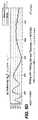
図1Aは、半導体ウェハ12の一部分の斜視図であり、これは中に接点穴13の2次元アレイを有する層12bを上に有するシリコン基板12aを有する。図1Bは、図1Aのウェハ12の、図1Aの線1B−1Bに沿う横断面図である。図1Bの横断面図は、図1Aの縮尺と同じ縮尺で描かれてはいない。図1Bに示されているように、接点穴のアレイ内の穴13の各々は直径Dを有し、穴はピッチPで間隔を置いて並べられている。層12bはhの厚さまたは高さを有し、接点穴13の側壁はシリコン基板12aの上面に対して角度Aをなす。 FIG. 1A is a perspective view of a portion of a
従来の方法では、D(穴13の直径)、ピッチP、高さまたは厚さh、側壁角A、または接点穴13のプロフィールまたは形状に関連する他のパラメータのような量を判定できるように、前に参照されたパラメータの全ては層12bの複素屈折率と共に構造のモデルに含められ、スペクトルと合致する最良のモデルパラメータを見出すために回帰が使用される。このような多数のパラメータを含むスペクトルの計算は時間を消費し、実時間で完了するためには実用的でない。前述した従来の方法の1つでは、膜厚の値を見出すために穴のない膜の隣接領域が独立に測定される。この測定された厚さ値は、構造モデルの独立変数の数を減らすために、中に穴を有する膜のための構造モデルにおいて後に使用され得る。しかし、図1Aおよび1Bのウェハ12により例示されているように、残りのパラメータの判定とは無関係にそのような別個の測定を行って層12bの厚さhを判定するための、接点穴13の存在しない層12bの余分の領域はない。 In a conventional manner, it is possible to determine quantities such as D (diameter of hole 13), pitch P, height or thickness h, sidewall angle A, or other parameter related to the profile or shape of
本発明は、穴アレイに関連するパラメータの測定のための構造モデルを簡単にするために、接点穴アレイに関連するパラメータをいろいろに変えない層の膜モデルを用いて始めに層12bの厚さhの近似値を見出すことができるという認識に基づく。そのようにして見出される厚さは、穴13の直径DがピッチP或いは穴間の間隔の三分の一未満である場合により正確である。そのとき、穴13により占められる体積率は0.1より僅かに小さい。そのような場合、接点穴のパラメータ(例えば、直径、ピッチ、側壁角など)をいろいろに変えない膜モデルは、多くの用途のために充分な精度の高さhの推定値を提供する。膜モデルを用いる前述したコンセプトを適用するための他の有利な条件は、或る波長における層12bの穴13のアレイから屈折した輻射の反射率が、穴直径Dのような回折構造に関連するパラメータによる影響を余り受けないということである。これらの問題点を検討する前に、まず、図1Aおよび1Bのウェハ12を測定するために使用され得る装置を説明するのが有益である。 In order to simplify the structural model for the measurement of the parameters associated with the hole array, the present invention begins with the thickness of the
図2は、本発明の好ましい実施形態を具体的に説明する分光スキャタロメータシステム10の略図である。図2に示されているように、システム10は、分光スキャタロメータ、分光楕円偏光計および分光反射計の特徴を有利に組み合わせられる。分光反射計または分光楕円偏光計は、膜モデルを用いて回折構造を含む層の膜厚を測定し、以下で説明される回折構造に関連するパラメータを判定するために接点穴13のアレイから回折した輻射のスペクトルを後に測定するために使用され得る。図2に示されているように、半導体ウェハ12は、シリコン基板12aと、膜内の接点穴のアレイのような2次元回折構造を中に有する基板上の(フォトレジストパターンのような)膜12bとを含むことができ、この膜は、少なくとも部分的に光伝導性であって、一定の膜厚hおよび屈折率(nおよびk、すなわち屈折率の実数成分および虚数成分)を有する。 FIG. 2 is a schematic diagram of a
ウェハを光学系に対して位置決めするためウェハを水平XY方向に移動させるためにXYZステージ14が使用される。以下で説明するように、ウェハ12のz高さを調整するためにもステージ14が使用され得る。図2に関して、白色光源22のような広帯域輻射源(或いは単一または複数の波長の輻射を供給する光源)は、偏りをランダム化してウェハを照明するための均一な光源を作り出すオプションの光ファイバケーブル24を通して光を供給する。好ましくは、光源22は少なくとも230〜800nmの範囲の波長を有する電磁輻射を供給する。ファイバ24から出ると、輻射は、スリットアパーチャおよびフォーカスレンズ(図示せず)を含むことのできる光学照明器を通過する。このスリットアパーチャは、出てきた光ビームに、調節され得る寸法の層12bの領域を結像させる。照明器26から出た光は、P偏光またはS偏光を有するもののような、層12bを照明する偏光サンプリングビーム30を生じさせるように偏光子28により偏光させられる。 An
サンプリングビーム30から生じた輻射は、層12bにより反射させられ、その反射した輻射のいろいろなスペクトル成分を検出するために検光子32を通して分光計34に渡される。分光楕円偏光計についてのもっと詳しい解説を得るためには、1997年3月4日に登録された米国特許第5,608,526号(特許文献1)を参照されたい。この特許は、その全体が本願明細書において参照により援用されている。 Radiation generated from the
膜厚を測定するためのシステム10の分光楕円偏光法モードでは、分光計34が光源22のスペクトル中の波長などの複数の波長の反射した光を検出しているときに偏光子28または検光子30(または両方)が(偏光子および検光子間に相対的回転運動を生じさせるために)回転させられ、その回転は当業者に知られた仕方でコンピュータ40により制御される。検出されたいろいろな波長における反射強度はコンピュータ40に供給され、これは以下でより詳しく説明する仕方で層12b(または層12bに似ているが中に穴を持っていない層)の膜厚と屈折率のnおよびkの値とを計算する。層12bに似ているが中に穴を持っていない層の膜厚と屈折率のnおよびkの値とは、当業者に知られている仕方で、または米国特許第5,608,526号(特許文献1)に記載されているように、導出され得る。 In the spectroscopic ellipsometry mode of the
膜厚を測定するためには分光楕円偏光法が好ましいけれども、或る用途では膜厚を測定するためには分光反射計(スペクトロリフレクトメータおよびスペクトロフォトメータとしても知られている)が適切である。この目的のために、レンズ23は光源22からの輻射を集めてビームスプリッタ52に向け、これは、入ってきたビームの一部を、輻射を層12bに収束させる集束レンズ54の方へ反射させる。層12bから反射した光は、レンズ54により集められ、ビームスプリッタ52を通過して分光反射計60内の分光計に進む。測定される単一またはいろいろな波長のスペクトル成分が検出され、そのような成分を表す信号が、例えば米国特許第5,747,813号(特許文献2)に記載されている仕方で膜厚と屈折率とを判定するためにコンピュータ40に供給される。分光反射計および分光楕円偏光計以外の分光装置、または偏光計および単一波長楕円偏光計または反射計のような他の装置も、層12bの膜厚を測定するために使用され得、本発明の範囲内にある。 Spectral ellipsometry is preferred for measuring film thickness, but for some applications, spectral reflectometers (also known as spectroreflectometers and spectrophotometers) are appropriate for measuring film thickness. . For this purpose, the
層12bの膜厚を判定するために使用され得るそのような分光装置の他の例は、カリフォルニア州サンタ クララのn&kテクノロジー・インク (n&k Technology Inc.)のn&kアナライザ (n&k Analyzer)を含み、ペンウェル・パブリッシング・カンパニーから出版されたソリッドステート・テクノロジーの1995年8月版からリプリントされたアイボックらによる「非晶質および多結晶質シリコン膜の光学的特性評価」 (“Optical Characterization of Amorphous and Polycrystalline Silicon Films," by Ibok et al., reprinted from August 1995 edition of Solid State Technology published by PennWell Publishing Company) (非特許文献1)、1986年11月15日の、フォルイらによる「非晶質半導体および非晶質誘電体についての光学的分散関係」,フィジカル・レビューB,第34巻,第10号,7018〜7026頁 (“Optical Dispersion Relations for Amorphous Semiconductors and Amorphous Dielectrics," by Forouhi et al., Physical Review B, vol. 34, no. 10, pp. 7018-7026, Nov. 15, 1986) (非特許文献2)、1988年7月15日の、フォルイらによる「結晶質半導体および誘電体の光学的特性」,フィジカル・レビューB,第38巻,第3号,1865〜1874頁 (“Optical Properties of Crystalline Semiconductors and Dielectrics," by Forouhi et al., Physical Review B, vol. 38, no. 3, pp. 1865-1874, Jul. 15, 1988) (非特許文献3)、および米国特許第4,905,170号(特許文献3)に記載されている。 Other examples of such spectroscopic devices that can be used to determine the thickness of
ウェハ12の高さを、分光楕円偏光法測定において適切な焦点調節を達成するために偏光子28、検光子32に関して調節する目的で、或いは分光反射計測定において集束レンズ54および分光反射計60に関して調節する目的で、ウェハの高さは測定前にステージ14によって調整される必要がある。この目的のために、層12bから反射してレンズ54により集められた輻射の一部分は、反射した像をパターンと比較するためにビームスプリッタ62により収束およびパターン認識ブロック64の方へ反射させられる。ブロック62は、その比較に関する情報を、ステージ14を制御するコンピュータ40に送る。ステージ14は、ウェハ12をシステム10の光学コンポーネントに関して適切な高さに移動させるためにウェハ12を垂直またはZ方向に上または下に移動させる。 For the purpose of adjusting the height of the
穴13のアレイからの回折は、前述したように図2の装置またはシステム10を用いて測定され得る。測定された回折から膜12bの膜厚が得られると、層12bについての構造モデルを簡単化するために膜厚値を用いてコンピュータ40により基準データベースが構築され得る。回折構造に関連するパラメータは、膜厚が得られた同じデータから(或いは、代わりに図2の装置を用いて別個の測定で得られた構造の回折データから)導出され得る。基準データベースの代わりに、そのように得られた前の膜厚値を固定されたパラメータとして用いて、または回折構造のパラメータと共に膜厚を変動させるパラメータ推定プロセスでシード値として用いて、線形または非線形の最適化プロセスを実行することもできる。別の代案では基準データベースと組み合わせて線形または非線形の最適化プロセスを用いることもできる。 Diffraction from the array of
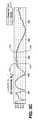
システム10により測定される反射率が或る波長範囲内では穴直径Dの変化の結果としては著しく変化しないということが見出されている。これを図3A〜3Cに示す。例えば、図3Aでは、穴の直径はおよそ120nmであり、接点穴アレイは240nmのピッチを有するが、この図において実線で示されているように、システム10により測定される反射率は、穴の直径が5nmも変化したときに実質的に同じままである。図3Aにおいて、点線の曲線はS偏光成分の反射率であり、実線の曲線は5nmの穴直径変化による反射率の変化である。穴のアレイが約240nmのピッチを有し、穴の直径は約120nmである図3Aから明らかなように、500nmより上の波長では、5nmに及ぶ穴直径変化にもかかわらず、反射率は実質的に一定のままである。図3Bおよび3Cは、穴直径約150nmおよびピッチ約300nm(図3B)、並びに穴直径約180nmおよびピッチ約360nm(図3C)での同じ現象を示す。図3Bおよび3Cの各々において、また、点線の曲線はS偏光成分の反射率を表し、実線の曲線は5nmの直径変化による反射率の変化を表す。図3A〜3Cにおいて、パラメータCD、すなわち限界寸法は、接点穴13の直径である。 It has been found that the reflectance measured by the
前述したことから、層12bの厚さまたは高さの正確な推定値を得るために膜モデルを使用することが可能であることは明らかであり、その膜モデルは穴直径をパラメータ化せず、変化させない。これは、スペクトルの赤および赤外部分或いは図3A〜3Cに示されている約500nmより上の波長範囲などの一定の限られた波長範囲においてのみ膜モデルが構築される場合に、特に当てはまる。構造自体に関連するパラメータがモデルにおいて変化させられないけれども、膜の中または近くの何らかの回折構造の存在の効果を考慮するように改変された膜モデルを採用するのが好ましい。中に回折格子を有する膜の厚さを計算するための膜モデルは当業者に知られ、本願明細書では詳しくは説明しない。そのような膜モデルに関するさらなる詳細については、チャールズ・ダブリュー・ハガンスらによる「円錐マウントにおけるゼロ次ラメラ格子の有効媒質理論」,J.Opt.Soc.Am.A,1993年10月19日,第10巻,第10号,2217〜2225頁 (“Effective-Medium Theory of Zeroth-Order Lamellar Gratings in Conical Mountings," by Charles W. Haggans et al., J. Opt. Soc. Am. A, October 19, 1993, Volume 10, No. 10, Pages 2217-2225) (非特許文献4)、ピー・ララネらによる「古典的マウントにおけるサブ波長格子の高次有効媒質理論:体積ホログラムへの応用」,J.Opt.Soc.Am.A,第15巻,第7号,1998年7月,1843〜1851頁 (“High-Order Effective-Medium Theory of Subwavelength Gratings in Classical Mounting: Application to Volume Holograms," by P. Lalanne et al., J. Opt. Soc. Am. A, Volume 15, No. 7, July 1998, Pages 1843-1851)(非特許文献5)、ピー・レラネによる「サブ波長周期構造の有効媒質理論について」,現代光学ジャーナル,1996年,第43巻,第10号,2063〜2085頁 (“On the Effective Medium Theory of Subwavelength Periodic Structures," P. Lelanne, Journal of Modern Optics, 1996, Volume 43, No. 10, Pages 2063-2085)(非特許文献6)、および「非準安定状態限界における2次元サブ波長格子の有効媒質理論」,J.Opt.Soc.Am.A,第15巻,第6号,1998年6月,1577〜1585頁 (“Effective Medium Theory of Two-Dimensional Subwavelength Gratings in the Non-Quasi-Static Limit," J. Opt. Soc. Am. A, Volume 15, No. 6, June 1998, Pages 1577-1585)(非特許文献7)を参照されたい。 From the foregoing it is clear that a membrane model can be used to obtain an accurate estimate of the thickness or height of the
膜モデルを用いて、図1Aおよび1Bの層12bの厚さhを回帰アルゴリズムを用いて見出すことができる。回帰アルゴリズムは当業者に知られ、ここでは詳しく説明しない。回帰法の説明についてはハーランド・ジー・トンプキンスおよびウィリアム・エイ・マクガンによる「分光楕円偏光法および反射計測:ユーザのガイド」,ジョン・ワイリー・アンド・サンズ・インコーポレイション,ニューヨーク,1999年,101〜107頁 (“Spectroscopic Ellipsometry and Reflectometry: A User's Guide," by Harland G. Tompkins and William A. McGahan, John Wiley & Sons, Inc., New York, 1999, Pages 101-107)(非特許文献8)を参照されたい。 Using the membrane model, the thickness h of the
図4Aは、層の厚さの基準値を提供するために、層12bに似ているが中に接点穴を持たない層が測定されたときの、1つのスペクトルにわたっての、楕円偏光パラメータαの測定された値と、膜モデルにより計算された値との比較を示すグラフ的プロットである。楕円偏光パラメータαおよびβの説明については、バーヌーらの「偏光解析法」,技術者の技術,R6490,1〜16頁(1990) (Bernoux et al., “Ellipsometrie," Techniques de l'Ingenieur, R6490, pp.1-16 (1990))(非特許文献9)を参照されたい。図4Aに示されているように、αの測定された値は軽快な点線で示され、モデルにより予測された値はより重い点線で示されている。図4Aに示されているように、測定された値とモデルにより予測された値とは一致し、実質的に同じである。図4Bおよび4Dに示されているように、同じことが楕円偏光パラメータβとP偏光成分の反射率とに当てはまると思われる。S偏光成分の反射率に関して、測定された値102は、予測された値には現れない少量の振動を450〜500nm波長の間で示し、500〜600nmの波長範囲ではモデルにより予測された値(104)より僅かに高い。このようなずれは別として、楕円偏光パラメータと反射率との実際の測定された値は、膜モデルにより予測された値と実質的に一致する。図4A〜4Bに示されている結果では、屈折率変数nおよびkは膜モデルでは変えられ、厚さも変える。回帰により到達した厚さは3967オングストロームである。 FIG. 4A illustrates the elliptical polarization parameter α over one spectrum when a layer similar to
図5A〜5Dは、中に接点穴を有する層12bが測定されたときの、楕円偏光パラメータαおよびβとSおよびP偏光成分の反射率との、測定された値と修正された膜モデルにより予測される値とを比較した比較をグラフを用いて示す。図5A〜5Dに示されている結果では、有効屈折率変数nおよびkの他にモデルにおいて層12bの厚さも変えられる。しかし、直径または穴のプロフィールのような接点穴に関するパラメータは変えられない。図4A〜4Dと図5A〜5Dを比較することから明らかなように、グラフ的プロットの両方のセットにおいて測定された値とモデルにより予測された値とは実質的に同じである。図4Cおよび5Cの測定された値112は、400から500nmの間では実質的に同じ振動の挙動を示し、500から600nmの間では予測された値114より僅かに高い。 FIGS. 5A-5D show the measured values of the elliptical polarization parameters α and β and the reflectance of the S and P polarization components and the modified film model when the
図5A〜5Dに示されている測定および構造モデルから回帰により得られた層12bの厚さは3970.08オングストロームであり、これは、中に穴のない膜パッドの測定から得られた値3967オングストロームに近い。これは、実際に、層内の回折構造の存在を考慮した層12bの修正されたモデルを用いて得られた厚さが、中に接点穴のない膜を測定することから得られた厚さと一致することを証明している。修正されたモデルでは、いろいろに変えられる屈折率パラメータnおよびkは図2のシステム10により見られる中に接点穴13を有する層12bについての実効値であって、層12bの材料の屈折率の値とは異なり得る。前述したように、精度を改善するために、赤および近赤外波長のみ、または500nm以上、或いは反射率が回折構造の寸法またはプロフィールの変化による影響を余り受けない他の波長範囲などにおけるデータなどの、限られた波長範囲において回帰プロセスが測定されたデータおよびモデルに適用され得る。 The thickness of
図6A〜6Dは、中に接点穴を有する層12bが測定されたときの、楕円偏光パラメータαおよびβとSおよびP偏光成分の反射率との、測定された値と修正された膜モデルにより予測された値とを比較した比較をグラフを用いて示す。図6A〜6Dに示されている結果では、モデルにおいて層12bの厚さが変えられるが、実効屈折率変数nおよびkは変えられない。図5A〜5Dと図6A〜6Dを比較すれば明らかであるように、実効屈折率変数nおよびkを変えずに厚さだけを変えると(図6A〜6D)、実効屈折率変数nおよびkも変えた場合(図5A〜5D)より劣る結果が生じる。図6A〜6Dに示されているように、測定された値202,212,222,232は、修正されたモデルにより予測される値204,214,224,234に近いけれども幾つかの波長範囲において一致しない。従って、厚さだけを変えることは或る目的のためには充分であるが、実効屈折率変数nおよびkも変化させるのが好ましい。 6A-6D show the measured values of the elliptical polarization parameters α and β and the reflectivity of the S and P polarization components and the modified film model when the
図7は、層12bに類似するが中に穴のない膜と層12bとについてのnおよびkの回帰させられた値の比較を示すグラフ的プロットである。図7に示されているように、中に穴のない膜についてのnおよびkの値302および312は、中に穴を有する層12bについての値304および314とは異なる。前述した層の厚さを導出するための回帰プロセスもnおよびkについての値をもたらすことができる。従って、或る用途について、膜のための前述した回帰プロセスで得られるnおよびkについての値は中に穴を有する層12bについての値とは著しく異なり得るので、それらは、後に穴アレイからの回折についてモデルを構築するときに使用される必要のある変数の数をさらに減らすためには役立たないかもしれない。それでも、膜についてのnの回帰させられた値は格子についての値と大幅には違わないことが観察されているので、或る用途について、接点穴アレイからの回折をモデル化するときに変えられなければならないモデルパラメータの数をさらに減らすために、層の厚さを得るときに前述したプロセスで得られたnの回帰させられた値を使用することが可能である。或いは、層12bの厚さが良く確認されているときには(例えば、安定した製造プロセスにおいて)、有効媒質理論を取り入れた膜モデルを用いて導出された率の値(n&k)は、回折構造のプロフィールパラメータのうちのあるもの(例えば、穴直径)についての線形または非線形の最適化プロセスにおいてシードまたは開始値を生成し、これによりこのプロセスの収束を速めるために、使用され得る。 FIG. 7 is a graphical plot showing a comparison of the regressed values of n and k for a film similar to
層の厚さの推定値(およびオプションでnの値も)が前述したように得られた後、中に穴を有する層12bからの回折の検出された信号スペクトルを有するモデルが、米国特許第6,590,656号(特許文献4)により詳しく説明されている仕方で構築され、この特許はその全体が本願明細書において参照により援用されている。膜厚と回折構造に関連するパラメータとの両方の別個の連続した導出のために同じ回折データが使用される実施形態では、そのように得られた膜厚を用いてそのようなパラメータが導出される。回折構造に関連するパラメータが厚さ導出のために用いられるものとは異なるデータから得られる代替の実施形態では、図2のシステム10は、照明ビームを層に向けて米国特許第6,590,656号(特許文献4)により詳しく説明されている仕方で層からのゼロ次回折を好ましくは複数の波長において検出することによって、層12b内の穴13のアレイから回折した輻射を測定するために再び使用されるが、或る用途のためには単一の波長で充分である。両方の実施形態において、測定されたデータおよび構築されたモデルに回帰アルゴリズムが適用され、それはピッチ、限界寸法(線の幅または穴の直径)、側壁角またはプロフィールのような、回折構造に関連するパラメータの値を見出すために推定された層の厚さ(およびオプションでnの値も)を使用する。回帰アルゴリズムによりいろいろに変えられるパラメータは、回折構造に関連するものを含み、層12bの厚さを含まない。層の厚さを推定するためのプロセスから有効なnおよびkの(またはkだけの)値が分からない場合には、nおよびk(またはkだけ)はプロセスにおいていろいろに変えられるパラメータとして含まれても良い。回折構造に関連するパラメータを見出すためのモデルは、2000年12月19日に出願された「光学分光システムを使用するパラメトリック・プロフィーリング」という米国特許出願第09/741,663号(特許文献5)と、2000年9月27日に出願された「散乱計測定の改良システムおよび応用」という米国特許出願第09/671,715号(特許文献6)とに説明され、これら特許出願はその全体が本願明細書において参照により援用されている。これらのパラメータの値は、システム10により測定された強度または楕円偏光パラメータデータを用いて見出され得る。 After an estimate of the layer thickness (and optionally also the value of n) is obtained as described above, a model having a detected signal spectrum of diffraction from a
その2つの実施形態が図8に示されている。図8に示されているように、複数の波長の電磁輻射のビームが、周期的回折構造を含む層を有するサンプルに向けられる。回折構造からの複数の波長のビームの回折が検出される。層の膜モデルを使用する層の厚さの値が、検出された回折から、または、構造がビームにより照明されてその構造によるビームの回折がデータを得るために検出される別個の測定で得られたデータから、見出される。その後、回折構造に関連する1つ以上のパラメータが、厚さ値と検出された回折とを用いて判定される。 Two such embodiments are shown in FIG. As shown in FIG. 8, a beam of electromagnetic radiation of multiple wavelengths is directed to a sample having a layer that includes a periodic diffractive structure. Diffraction of multiple wavelength beams from the diffractive structure is detected. The layer thickness value using the layer film model is obtained from the detected diffraction or in a separate measurement where the structure is illuminated by the beam and the diffraction of the beam by the structure is detected to obtain data. From the data obtained. Thereafter, one or more parameters associated with the diffractive structure are determined using the thickness value and the detected diffraction.
第1のステップで得られた膜厚に関する情報は、格子プロフィールパラメータ推定プロセスの前にまたはその間に、光学的照明および収集角度並びにアパーチャサイズが回折構造の測定のために最善であることを確認するために使用され得る。或る多層膜構造について、格子プロフィールパラメータを判定するための最も敏感な光学的条件は、膜厚と共に変化し得る。第1のパラメータ推定ステップで導出された膜厚に基づいて、調整可能または選択可能な角度およびアパーチャサイズを取り入れた測定システムについて、第1のステップと同じサイト或いは同じウェハ上または次のウェハ上の次のサイトについての後の分光および角度測定データの感度を最大にするために、光学的照明および収集角度並びにアパーチャサイズが調整または選択可能である。 Information on film thickness obtained in the first step confirms that the optical illumination and collection angle and aperture size are best for the measurement of diffractive structures before or during the grating profile parameter estimation process Can be used for. For some multilayer structures, the most sensitive optical conditions for determining lattice profile parameters can vary with film thickness. Based on the film thickness derived in the first parameter estimation step, for a measurement system incorporating an adjustable or selectable angle and aperture size, on the same site or on the same wafer as the first step or on the next wafer Optical illumination and collection angles and aperture sizes can be adjusted or selected to maximize the sensitivity of subsequent spectroscopic and angle measurement data for the next site.
種々の実施形態を参照して本発明を前に説明してきたが、添付されている特許請求の範囲およびその同等物によってのみ定義されるべき発明の範囲から逸脱せずに変更および改変をなし得ることが理解される。例えば、穴の2次元アレイに関連するパラメータを測定するために実施形態を説明してきたが、柱の2次元アレイ、格子線または穴の1次元アレイのような他の回折構造に関連するパラメータを測定するために同じ実施形態が使用され得る。本願明細書において参照された全ての参考文献は、その全体が本願明細書において参照により援用されている。 Although the invention has been described above with reference to various embodiments, changes and modifications can be made without departing from the scope of the invention which is to be defined only by the appended claims and their equivalents. It is understood. For example, while embodiments have been described to measure parameters associated with a two-dimensional array of holes, parameters associated with other diffractive structures such as a two-dimensional array of pillars, a grid line or a one-dimensional array of holes may be used. The same embodiment can be used to measure. All references referred to herein are hereby incorporated by reference in their entirety.
Claims (28)
Translated fromJapanese複数の波長の電磁輻射の第1のビームを前記周期的回折構造に向けるステップと、
前記回折構造からの前記複数の波長での前記第1のビームの回折を検出するステップと、
前記層の膜モデルを用いて前記層の厚さ値を見出すステップと、
前記厚さ値と検出された前記回折とを用いて前記回折構造に関連する1つ以上のパラメータを判定するステップと、
を含む方法。A method for measuring a sample having a layer comprising a periodic diffractive structure, comprising:
Directing a first beam of electromagnetic radiation of a plurality of wavelengths to the periodic diffractive structure;
Detecting diffraction of the first beam at the plurality of wavelengths from the diffractive structure;
Finding a thickness value of the layer using a film model of the layer;
Determining one or more parameters associated with the diffractive structure using the thickness value and the detected diffraction;
Including methods.
前記見出すステップは、反射計または楕円偏光計を使用する方法。The method of claim 1, wherein
The finding step is a method using a reflectometer or an ellipsometer.
前記見出すステップは、分光反射計または分光楕円偏光計を使用する方法。The method of claim 1, wherein
The finding step is a method using a spectral reflectometer or a spectroscopic ellipsometer.
前記見出すステップは膜モデルを使用し、この膜モデルは選択された波長の範囲の中のデータに限定されたデータを使用し、その範囲における前記周期的回折構造の反射率は、前記構造の寸法またはプロフィールの変化に対する感受性が、前記範囲の外側の波長におけるそのような変化に対する感受性よりも低い方法。The method of claim 1, wherein
The finding step uses a film model, which uses data limited to data in a selected wavelength range, and the reflectivity of the periodic diffractive structure in that range is the dimension of the structure. Or a method that is less sensitive to changes in the profile than such changes in wavelengths outside the range.
前記見出すステップは、赤および近赤外範囲の中の波長のデータに限定されたデータを使用する膜モデルを使用する方法。The method of claim 4, wherein
The finding step uses a film model that uses data limited to data for wavelengths in the red and near infrared ranges.
前記見出すステップは膜モデルを使用し、この膜モデルは選択された波長におけるデータに限定されたデータを使用し、それらの波長における前記周期的回折構造の反射率は、前記構造の寸法またはプロフィールの変化に対する感受性が、前記選択された波長とは異なる波長におけるそのような変化に対する感受性よりも低い方法。The method of claim 1, wherein
The finding step uses a film model, which uses data limited to data at selected wavelengths, and the reflectivity of the periodic diffractive structure at those wavelengths is the size or profile of the structure. A method that is less sensitive to changes than such changes at wavelengths different from the selected wavelength.
前記見出すステップは、
前記周期的回折構造の少なくとも一部分を含む前記層のセクションに複数の波長の電磁輻射の第2のビームを向けるステップと、
前記第2のビームの強度または楕円偏光データを、それが前記層の前記セクションにより改変された後に、検出するステップと、
を含む方法。The method of claim 1, wherein
The finding step includes
Directing a second beam of electromagnetic radiation of a plurality of wavelengths to a section of the layer that includes at least a portion of the periodic diffractive structure;
Detecting the intensity or elliptical polarization data of the second beam after it has been modified by the section of the layer;
Including methods.
前記見出すステップは、前記層の厚さと屈折率とを含むパラメータを使用するが前記回折構造の寸法またはプロフィールに関連するパラメータを使用しない膜モデルを使用する方法。The method of claim 7, wherein
The finding step uses a film model that uses parameters including thickness and refractive index of the layer, but does not use parameters related to the size or profile of the diffractive structure.
前記見出すステップは、前記層の屈折率に関連するパラメータの値を変える方法。The method of claim 8, wherein
The finding step changes the value of a parameter related to the refractive index of the layer.
前記見出すステップは、検出された回折から前記厚さ値を見出す方法。The method of claim 1, wherein
The finding step finds the thickness value from the detected diffraction.
前記見出すステップは、前記層の厚さと屈折率とを含むパラメータを使用するが前記回折構造の寸法またはプロフィールに関連するパラメータを使用しない膜モデルを使用する方法。The method of claim 10, wherein:
The finding step uses a film model that uses parameters including thickness and refractive index of the layer, but does not use parameters related to the size or profile of the diffractive structure.
前記見出すステップは、前記層の屈折率に関連するパラメータの値を変える方法。The method of claim 11 wherein:
The finding step changes the value of a parameter related to the refractive index of the layer.
前記見出すステップは、前記層の厚さと屈折率とを含むパラメータを使用するが前記回折構造の寸法またはプロフィールに関連するパラメータを使用しない膜モデルを使用する方法。The method of claim 1, wherein
The finding step uses a film model that uses parameters including thickness and refractive index of the layer, but does not use parameters related to the size or profile of the diffractive structure.
前記見出すステップは、前記層の屈折率に関連するパラメータの値を変える方法。The method of claim 1, wherein
The finding step changes the value of a parameter related to the refractive index of the layer.
前記見出すステップは、少なくとも前記構造の前記回折が検出された部分を含む前記層のセクションを測定することにより前記厚さ値を見出す方法。The method of claim 1, wherein
The finding step finds the thickness value by measuring a section of the layer including at least a portion of the structure where the diffraction is detected.
前記判定するステップは、前記厚さ値を使用する回帰アルゴリズムを適用するステップを含む方法。The method of claim 1, wherein
The method of determining includes applying a regression algorithm using the thickness value.
前記判定するステップは、前記回折構造に関連する前記1つ以上のパラメータを判定する回帰アルゴリズムを適用するステップを含む方法。The method of claim 1, wherein
The method of determining includes applying a regression algorithm to determine the one or more parameters associated with the diffractive structure.
前記回帰アルゴリズムは前記回折構造の寸法および/またはプロフィールに関連するパラメータのみの値を変え、前記変えられるパラメータは前記層の厚さを含まない方法。The method of claim 17, wherein
The regression algorithm changes only the values of parameters related to the size and / or profile of the diffractive structure, and the changed parameters do not include the layer thickness.
前記変えられるパラメータは、前記構造の幅または直径と側壁角とに関連する方法。The method of claim 18, wherein:
The variable parameter is a method related to the width or diameter of the structure and the sidewall angle.
前記検出するステップは、前記回折から強度または楕円偏光データを検出し、前記判定するステップは、検出した強度または楕円偏光データを用いて前記回折構造に関連する前記1つ以上のパラメータを判定する方法。The method of claim 1, wherein
The detecting step detects intensity or elliptical polarization data from the diffraction, and the determining step uses the detected intensity or elliptical polarization data to determine the one or more parameters associated with the diffractive structure. .
前記判定するステップは、前記厚さ値を用いて基準データベースを構築するステップを含む方法。The method of claim 1, wherein
The determining step includes building a reference database using the thickness value.
前記判定するステップは、前記厚さ値を固定パラメータとして用いる線形または非線形の最適化プロセスをさらに含む方法。The method of claim 1, wherein
The determining step further includes a linear or non-linear optimization process using the thickness value as a fixed parameter.
前記判定するステップは、前記回折構造の前記パラメータと共に前記厚さ値が変動するパラメータ推定プロセスで前記厚さ値をシード値として用いる線形または非線形の最適化プロセスを含む方法。The method of claim 1, wherein
The determining step includes a linear or non-linear optimization process that uses the thickness value as a seed value in a parameter estimation process in which the thickness value varies with the parameter of the diffractive structure.
前記見出すステップは、膜モデルを用いて前記層の屈折率の値(単数または複数)も見出す方法。The method of claim 1, wherein
The finding step is a method of finding the refractive index value (s) of the layer using a film model.
前記回折構造の前記パラメータの幾つかについて線形または非線形の最適化プロセスにおいてシードまたは開始値を生成し、これによりこのプロセスの収束を速めるために、前記判定するステップは前記層の前記屈折率の値(単数または複数)を使用するステップを含む方法。25. The method of claim 24, wherein
In order to generate a seed or starting value in a linear or non-linear optimization process for some of the parameters of the diffractive structure, thereby speeding up the convergence of the process, the determining step includes the value of the refractive index of the layer. A method comprising the step of using (one or more).
前記方法は、前記回折構造のパラメータの変化に対するデータの感度を最大にするために、前記厚さ値に応じて、前記第1のビームの光学的照明角度および/またはアパーチャサイズおよび/または前記検出するステップのための収集角度を調整しまたは選択するステップをさらに含む方法。The method of claim 1, wherein
In order to maximize the sensitivity of the data to changes in the parameters of the diffractive structure, the method depends on the thickness value and the optical illumination angle and / or aperture size and / or the detection of the first beam. Adjusting or selecting a collection angle for the step of performing.
前記見出すステップは前記向けるステップおよび検出するステップに先行して、前記周期的回折構造の少なくとも一部分を含む前記層のセクションの前記厚さ値を見出し、前記向けるステップは向け、前記検出するステップは前記セクションからまたは前記周期的回折構造の少なくとも一部分を含む前記層の別のセクションから検出する方法。The method of claim 26.
The finding step finds the thickness value of the section of the layer including at least a portion of the periodic diffractive structure prior to the directing and detecting step, the directing step is directed, and the detecting step is Detecting from a section or from another section of the layer comprising at least a part of the periodic diffractive structure.
前記見出すステップは前記向けるステップおよび検出するステップに先行して、前記周期的回折構造の少なくとも一部分を含む前記層のセクションの前記厚さ値を見出し、前記厚さ値がそれから見出されたところのものとは異なる周期的回折構造を含む層のセクションに前記向けるステップは前記第1のビームを向け、前記検出するステップはこのセクションから検出する方法。The method of claim 26.
The finding step finds the thickness value of the section of the layer that includes at least a portion of the periodic diffractive structure prior to the directing and detecting step, wherein the thickness value has been found therefrom. A method in which the step of directing to a section of the layer comprising a periodic diffractive structure different from that directs the first beam and the detecting step detects from this section.
Applications Claiming Priority (5)
| Application Number | Priority Date | Filing Date | Title |
|---|---|---|---|
| US64371105P | 2005-01-12 | 2005-01-12 | |
| US60/643,711 | 2005-01-12 | ||
| US11/329,500US7515253B2 (en) | 2005-01-12 | 2006-01-10 | System for measuring a sample with a layer containing a periodic diffracting structure |
| US11/329,500 | 2006-01-10 | ||
| PCT/US2006/001067WO2006076484A2 (en) | 2005-01-12 | 2006-01-11 | Periodic diffracting system for sample measurement |
Publications (3)
| Publication Number | Publication Date |
|---|---|
| JP2008530519Atrue JP2008530519A (en) | 2008-08-07 |
| JP2008530519A5 JP2008530519A5 (en) | 2009-02-26 |
| JP5341354B2 JP5341354B2 (en) | 2013-11-13 |
Family
ID=36678181
Family Applications (1)
| Application Number | Title | Priority Date | Filing Date |
|---|---|---|---|
| JP2007551372AExpired - Fee RelatedJP5341354B2 (en) | 2005-01-12 | 2006-01-11 | System for measuring a sample having a layer containing a periodic diffractive structure |
Country Status (4)
| Country | Link |
|---|---|
| US (2) | US7515253B2 (en) |
| JP (1) | JP5341354B2 (en) |
| KR (1) | KR101342410B1 (en) |
| WO (1) | WO2006076484A2 (en) |
Cited By (3)
| Publication number | Priority date | Publication date | Assignee | Title |
|---|---|---|---|---|
| JP2008098636A (en)* | 2006-10-13 | 2008-04-24 | Asml Netherlands Bv | Inspection method and apparatus, lithographic apparatus, lithographic processing cell and device manufacturing method |
| JP2010060388A (en)* | 2008-09-02 | 2010-03-18 | Tokyo Electron Ltd | Pattern shape inspection method and manufacturing method for semiconductor device |
| US8227265B2 (en) | 2009-07-22 | 2012-07-24 | Renesas Electronics Corporation | Method of measuring pattern shape, method of manufacturing semiconductor device, and process control system |
Families Citing this family (18)
| Publication number | Priority date | Publication date | Assignee | Title |
|---|---|---|---|---|
| US6483580B1 (en) | 1998-03-06 | 2002-11-19 | Kla-Tencor Technologies Corporation | Spectroscopic scatterometer system |
| JP4938219B2 (en)* | 2001-12-19 | 2012-05-23 | ケーエルエー−テンカー コーポレイション | Parametric profiling using optical spectroscopy systems |
| US7515253B2 (en)* | 2005-01-12 | 2009-04-07 | Kla-Tencor Technologies Corporation | System for measuring a sample with a layer containing a periodic diffracting structure |
| JP5186129B2 (en)* | 2006-08-25 | 2013-04-17 | 大日本スクリーン製造株式会社 | Method and apparatus for measuring groove pattern depth |
| US7729873B2 (en)* | 2007-08-28 | 2010-06-01 | Tokyo Electron Limited | Determining profile parameters of a structure using approximation and fine diffraction models in optical metrology |
| JP4950813B2 (en)* | 2007-08-30 | 2012-06-13 | 大日本スクリーン製造株式会社 | Spectral ellipsometer, film thickness measuring apparatus, and focus adjustment method of spectroscopic ellipsometer |
| US7930657B2 (en)* | 2008-01-23 | 2011-04-19 | Micron Technology, Inc. | Methods of forming photomasks |
| US8199321B2 (en)* | 2008-05-05 | 2012-06-12 | Applied Spectra, Inc. | Laser ablation apparatus and method |
| EP2251638B1 (en)* | 2009-05-12 | 2013-04-24 | LayTec Aktiengesellschaft | Method and apparatus for determining the layer thickness and the refractive index of a sample |
| US8441639B2 (en)* | 2009-09-03 | 2013-05-14 | Kla-Tencor Corp. | Metrology systems and methods |
| WO2011056892A1 (en)* | 2009-11-03 | 2011-05-12 | Applied Spectra, Inc. | Method for real-time optical diagnostics in laser ablation and laser processing of layered and structured materials |
| JP2012195096A (en)* | 2011-03-15 | 2012-10-11 | Canon Inc | Charged particle beam lens and exposure apparatus using the same |
| US20130341310A1 (en)* | 2012-06-22 | 2013-12-26 | Coherent Lasersystems Gmbh & Co. Kg | Monitoring method and apparatus for excimer laser annealing process |
| US9335276B2 (en) | 2014-03-03 | 2016-05-10 | Coherent Lasersystems Gmbh & Co. Kg | Monitoring method and apparatus for control of excimer laser annealing |
| US10458912B2 (en)* | 2016-08-31 | 2019-10-29 | Kla-Tencor Corporation | Model based optical measurements of semiconductor structures with anisotropic dielectric permittivity |
| US9976969B1 (en) | 2016-10-28 | 2018-05-22 | Coherent Lasersystems Gmbh & Co. Kg | Monitoring method and apparatus for excimer-laser annealing process |
| US10746530B2 (en)* | 2018-12-07 | 2020-08-18 | Onto Innovation Inc. | Optical metrology device for measuring samples having thin or thick films |
| DE102019213904A1 (en)* | 2019-09-12 | 2021-03-18 | Carl Zeiss Smt Gmbh | Method for detecting an object structure and device for carrying out the method |
Citations (8)
| Publication number | Priority date | Publication date | Assignee | Title |
|---|---|---|---|---|
| JPH08255751A (en)* | 1995-02-15 | 1996-10-01 | At & T Corp | Method and arrangement to characterize microsize pattern |
| JPH09237812A (en)* | 1995-12-28 | 1997-09-09 | Fujitsu Ltd | Processing dimension measuring method, semiconductor device manufacturing method, and quality control method |
| JP2002506198A (en)* | 1998-03-06 | 2002-02-26 | ケーエルエー−テンカー コーポレイション | Diffraction structure, underlying structure, wide band, polarization ellipsometry |
| JP2002139303A (en)* | 2000-11-01 | 2002-05-17 | Murata Mfg Co Ltd | Edge-detecting device for transparent body |
| US20020113966A1 (en)* | 2000-12-19 | 2002-08-22 | Shchegrov Andrei V. | Parametric profiling using optical spectroscopic systems |
| US20020128784A1 (en)* | 1998-03-18 | 2002-09-12 | David Scheiner | Method and apparatus for measurements of patterned structures |
| WO2003054475A2 (en)* | 2001-12-19 | 2003-07-03 | Kla-Tencor Technologies Corporation | Parametric profiling using optical spectroscopic systems |
| JP2003222616A (en)* | 2002-01-30 | 2003-08-08 | Seiko Instruments Inc | Thin film-evaluating apparatus due to beat light resonance |
Family Cites Families (167)
| Publication number | Priority date | Publication date | Assignee | Title |
|---|---|---|---|---|
| US3426201A (en) | 1965-10-12 | 1969-02-04 | Texas Instruments Inc | Method and apparatus for measuring the thickness of films by means of elliptical polarization of reflected infrared radiation |
| US3547074A (en) | 1967-04-13 | 1970-12-15 | Block Engineering | Apparatus for forming microelements |
| US3667846A (en) | 1969-07-28 | 1972-06-06 | Charles Nater | Optical surface inspection apparatus |
| US3671126A (en) | 1970-02-19 | 1972-06-20 | Ati Inc | Noncontacting optical probe |
| US4171917A (en) | 1974-07-02 | 1979-10-23 | Centre De Recherches Metallurgiques-Centrum Voor Research In De Metallurgie | Determining the profile of a surface of an object |
| US4039370A (en) | 1975-06-23 | 1977-08-02 | Rca Corporation | Optically monitoring the undercutting of a layer being etched |
| CA1043463A (en) | 1975-12-05 | 1978-11-28 | Paul A. Mueller | Lumber inspection and optimization system |
| JPS5335567A (en) | 1976-09-13 | 1978-04-03 | Shinetsu Chem Ind Co | Apparatus for measuring thickness of semiconductor wafer |
| US4173788A (en) | 1976-09-27 | 1979-11-06 | Atmospheric Sciences, Inc. | Method and apparatus for measuring dimensions |
| US4146327A (en) | 1976-12-27 | 1979-03-27 | Autech | Optical triangulation gauging system |
| US4303341A (en) | 1977-12-19 | 1981-12-01 | Rca Corporation | Optically testing the lateral dimensions of a pattern |
| US4200396A (en) | 1977-12-19 | 1980-04-29 | Rca Corporation | Optically testing the lateral dimensions of a pattern |
| US4141780A (en) | 1977-12-19 | 1979-02-27 | Rca Corporation | Optically monitoring the thickness of a depositing layer |
| US5280179A (en) | 1979-04-30 | 1994-01-18 | Sensor Adaptive Machines Incorporated | Method and apparatus utilizing an orientation code for automatically guiding a robot |
| US5164579A (en) | 1979-04-30 | 1992-11-17 | Diffracto Ltd. | Method and apparatus for electro-optically determining the dimension, location and attitude of objects including light spot centroid determination |
| US4373804A (en) | 1979-04-30 | 1983-02-15 | Diffracto Ltd. | Method and apparatus for electro-optically determining the dimension, location and attitude of objects |
| US4330213A (en) | 1980-02-14 | 1982-05-18 | Rca Corporation | Optical line width measuring apparatus and method |
| US5112131A (en) | 1981-02-27 | 1992-05-12 | Diffracto, Ltd. | Controlled machining of combustion chambers, gears and other surfaces |
| DE3270551D1 (en) | 1981-03-16 | 1986-05-22 | Energy Conversion Devices Inc | Optical methods for controlling layer thickness |
| US4516855A (en) | 1981-04-03 | 1985-05-14 | International Business Machines Corporation | Method and apparatus for determining the polarization state of a light wave field |
| SE444875B (en) | 1981-04-15 | 1986-05-12 | Crafon Ab | WANT TO MANUFACTURE THERMISTORS |
| JPS57187604A (en) | 1981-05-14 | 1982-11-18 | Toshiba Corp | Measurement device of profile |
| US4408884A (en) | 1981-06-29 | 1983-10-11 | Rca Corporation | Optical measurements of fine line parameters in integrated circuit processes |
| JPS58206120A (en) | 1982-05-26 | 1983-12-01 | Hitachi Ltd | Semiconductor formation process control method |
| JPS5999304A (en) | 1982-11-30 | 1984-06-08 | Asahi Optical Co Ltd | Method and apparatus for comparing and measuring length by using laser light of microscope system |
| JPS59140420A (en) | 1983-02-01 | 1984-08-11 | Canon Inc | Light source device using semiconductor laser |
| JPS59140420U (en) | 1983-03-09 | 1984-09-19 | 株式会社高岳製作所 | Outer insulation material of transformer coil |
| JPH0750664B2 (en) | 1983-06-23 | 1995-05-31 | 富士通株式会社 | Reticle inspection method |
| JPS6033003A (en) | 1983-08-03 | 1985-02-20 | Hitachi Ltd | Shape measuring device |
| JPS6074528A (en) | 1983-09-30 | 1985-04-26 | Fujitsu Ltd | Resist pattern inspection equipment |
| JPS6086843A (en) | 1983-10-19 | 1985-05-16 | Hitachi Ltd | Processing equipment with polarization analyzer |
| JPS60128602A (en) | 1983-12-16 | 1985-07-09 | 株式会社日立製作所 | Multiple multi-rotation volume |
| US4615620A (en)* | 1983-12-26 | 1986-10-07 | Hitachi, Ltd. | Apparatus for measuring the depth of fine engraved patterns |
| USRE33424E (en)* | 1983-12-26 | 1990-11-06 | Hitachi, Ltd. | Apparatus and method for measuring the depth of fine engraved patterns |
| US4672196A (en) | 1984-02-02 | 1987-06-09 | Canino Lawrence S | Method and apparatus for measuring properties of thin materials using polarized light |
| JPS60166808A (en) | 1984-02-10 | 1985-08-30 | Toshiba Corp | Shape measuring apparatus |
| JPS60236005A (en) | 1984-05-09 | 1985-11-22 | Nec Corp | Measuring method of line width |
| US4695162A (en) | 1984-05-24 | 1987-09-22 | Victor Company Of Japan, Ltd. | Film thickness measuring apparatus |
| US4653924A (en) | 1984-06-12 | 1987-03-31 | Victor Company Of Japan, Ltd. | Rotating analyzer type ellipsometer |
| JPS614906A (en) | 1984-06-19 | 1986-01-10 | Nec Corp | Measuring method of line width |
| JPS614905A (en) | 1984-06-19 | 1986-01-10 | Nec Corp | Measuring method of line width |
| JPS6139852A (en) | 1984-07-31 | 1986-02-26 | Toshiba Electric Equip Corp | Protecting circuit of phase controller |
| DE3434575C1 (en) | 1984-09-20 | 1986-03-13 | Sagax Instrument AB, Sundbyberg | Ellipsometric device for examining the physical properties of the surface of a sample |
| US4687325A (en) | 1985-03-28 | 1987-08-18 | General Electric Company | Three-dimensional range camera |
| US4689491A (en) | 1985-04-19 | 1987-08-25 | Datasonics Corp. | Semiconductor wafer scanning system |
| US4710642A (en) | 1985-08-20 | 1987-12-01 | Mcneil John R | Optical scatterometer having improved sensitivity and bandwidth |
| US4668860A (en) | 1985-10-09 | 1987-05-26 | Optical Coating Laboratory, Inc. | Scattermeter using polarized light to distinguish between bulk and surface scatter |
| JPS62150251A (en) | 1985-12-24 | 1987-07-04 | Nec Corp | Data base type photomask inspecting device |
| JPH0523620Y2 (en) | 1986-02-12 | 1993-06-16 | ||
| US5329357A (en) | 1986-03-06 | 1994-07-12 | Sopra-Societe De Production Et De Recherches Appliquees | Spectroscopic ellipsometry apparatus including an optical fiber |
| FR2597976B1 (en) | 1986-04-24 | 1990-11-09 | Tissier Annie | METHOD FOR MEASURING CHARACTERISTIC PARAMETERS OF A THIN FILM AND APPARATUS FOR CARRYING OUT SAID METHOD |
| FR2605100B1 (en) | 1986-10-10 | 1988-12-09 | Labo Electronique Physique | OPTICAL DEVICE FOR ILLUMINATING A SAMPLE FOR A HIGH SIDE RESOLUTION SPECTROSCOPIC ELLIPSOMETER |
| JPH0769154B2 (en) | 1987-06-10 | 1995-07-26 | 富士写真フイルム株式会社 | Shape measurement method of resist pattern |
| JPS6428509A (en) | 1987-07-23 | 1989-01-31 | Nippon Kokan Kk | Apparatus for measuring thickness of film |
| US4905170A (en) | 1987-11-12 | 1990-02-27 | Forouhi Abdul R | Method and apparatus of determining optical constants of amorphous semiconductors and dielectrics |
| JPH01211937A (en) | 1988-02-18 | 1989-08-25 | Mitsubishi Metal Corp | Evaluation of strength of damage to wafer with distortion |
| FR2628211B1 (en) | 1988-03-04 | 1993-05-14 | Vareille Aime | ELLIPSOMETRY ANALYZER, METHOD OF ELLIPSOMETRIC ANALYSIS OF A SAMPLE AND APPLICATION TO MEASUREMENT OF VARIATION IN THICKNESS THICKNESS |
| JPH01285806A (en) | 1988-05-12 | 1989-11-16 | Nikon Corp | Groove shape measuring device |
| US5393624A (en) | 1988-07-29 | 1995-02-28 | Tokyo Electron Limited | Method and apparatus for manufacturing a semiconductor device |
| SU1695145A1 (en) | 1988-08-03 | 1991-11-30 | Институт Радиотехники И Электроники Ан Ссср | Ellipsometer |
| US4964726A (en) | 1988-09-27 | 1990-10-23 | General Electric Company | Apparatus and method for optical dimension measurement using interference of scattered electromagnetic energy |
| NL8802920A (en) | 1988-11-28 | 1990-06-18 | Hoogovens Groep Bv | COATING THICKNESS GAUGE. |
| US4991971A (en) | 1989-02-13 | 1991-02-12 | United Technologies Corporation | Fiber optic scatterometer for measuring optical surface roughness |
| US5076696A (en) | 1989-03-16 | 1991-12-31 | The Johns Hopkins University | Dynamic imaging microellipsometry |
| JPH0722483Y2 (en) | 1989-03-28 | 1995-05-24 | 川崎重工業株式会社 | Rotary actuator |
| DE3914631A1 (en) | 1989-05-03 | 1990-11-08 | Basf Ag | METHOD FOR EXAMINING THE PHYSICAL PROPERTIES OF THIN LAYERS |
| US5042951A (en) | 1989-09-19 | 1991-08-27 | Therma-Wave, Inc. | High resolution ellipsometric apparatus |
| US4999014A (en) | 1989-05-04 | 1991-03-12 | Therma-Wave, Inc. | Method and apparatus for measuring thickness of thin films |
| JPH0375504A (en) | 1989-08-18 | 1991-03-29 | Citizen Watch Co Ltd | Measuring method for very small dimension |
| JP3187827B2 (en) | 1989-12-20 | 2001-07-16 | 株式会社日立製作所 | Pattern inspection method and apparatus |
| US5166752A (en) | 1990-01-11 | 1992-11-24 | Rudolph Research Corporation | Simultaneous multiple angle/multiple wavelength ellipsometer and method |
| DE4105192C2 (en) | 1990-02-26 | 1996-07-04 | Stefan Oelckers | Method for determining surface roughness and the like |
| JPH0424541A (en) | 1990-05-21 | 1992-01-28 | Mitsui Mining & Smelting Co Ltd | Method and apparatus for measuring internal defect |
| JP2594685B2 (en) | 1990-06-06 | 1997-03-26 | 山形日本電気株式会社 | Wafer slip line inspection method |
| US5091320A (en) | 1990-06-15 | 1992-02-25 | Bell Communications Research, Inc. | Ellipsometric control of material growth |
| US5241369A (en) | 1990-10-01 | 1993-08-31 | Mcneil John R | Two-dimensional optical scatterometer apparatus and process |
| US5114233A (en) | 1990-10-09 | 1992-05-19 | At&T Bell Laboratories | Method for inspecting etched workpieces |
| US5032734A (en) | 1990-10-15 | 1991-07-16 | Vti, Inc. | Method and apparatus for nondestructively measuring micro defects in materials |
| JPH04176143A (en) | 1990-11-08 | 1992-06-23 | Nec Corp | Wafer pattern form inspecting device |
| JP2927934B2 (en) | 1990-11-16 | 1999-07-28 | 株式会社リコー | Thin film measurement method and apparatus |
| IL96483A (en) | 1990-11-27 | 1995-07-31 | Orbotech Ltd | Optical inspection method and apparatus |
| EP0527230B1 (en) | 1991-01-30 | 1996-06-05 | Nkk Corporation | Ellipsometer |
| JPH0774088B2 (en) | 1991-02-19 | 1995-08-09 | 洋三 山本 | Aggregate for concrete |
| US5164790A (en) | 1991-02-27 | 1992-11-17 | Mcneil John R | Simple CD measurement of periodic structures on photomasks |
| US5674652A (en) | 1991-02-28 | 1997-10-07 | University Of New Mexico | Diffracted light from latent images in photoresist for exposure control |
| DE4108329C2 (en) | 1991-03-14 | 1993-10-14 | Plasmos Gmbh Prozesstechnik | Method for determining material parameters, namely thickness, refractive index and absorption coefficient, of individual layers |
| JP3323537B2 (en) | 1991-07-09 | 2002-09-09 | キヤノン株式会社 | Microstructure evaluation device and microstructure evaluation method |
| US5337146A (en) | 1992-03-30 | 1994-08-09 | University Of New Orleans | Diffraction-grating photopolarimeters and spectrophotopolarimeters |
| US5486919A (en) | 1992-04-27 | 1996-01-23 | Canon Kabushiki Kaisha | Inspection method and apparatus for inspecting a particle, if any, on a substrate having a pattern |
| US5313044A (en) | 1992-04-28 | 1994-05-17 | Duke University | Method and apparatus for real-time wafer temperature and thin film growth measurement and control in a lamp-heated rapid thermal processor |
| US5386317A (en) | 1992-05-13 | 1995-01-31 | Prometrix Corporation | Method and apparatus for imaging dense linewidth features using an optical microscope |
| US5747813A (en) | 1992-06-16 | 1998-05-05 | Kla-Tencop. Corporation | Broadband microspectro-reflectometer |
| US5494829A (en) | 1992-07-31 | 1996-02-27 | Biostar, Inc. | Devices and methods for detection of an analyte based upon light interference |
| US5337150A (en) | 1992-08-04 | 1994-08-09 | Hughes Aircraft Company | Apparatus and method for performing thin film layer thickness metrology using a correlation reflectometer |
| US5361137A (en) | 1992-08-31 | 1994-11-01 | Texas Instruments Incorporated | Process control for submicron linewidth measurement |
| US5504582A (en) | 1992-09-18 | 1996-04-02 | J. A. Woollam Co. Inc. | System and method for compensating polarization-dependent sensitivity of dispersive optics in a rotating analyzer ellipsometer system |
| US5666201A (en) | 1992-09-18 | 1997-09-09 | J.A. Woollam Co. Inc. | Multiple order dispersive optics system and method of use |
| US5521706A (en) | 1992-09-18 | 1996-05-28 | J. A. Woollam Co. Inc. | System and method for compensating polarization-dependent sensitivity of dispersive optics in a rotating analyzer ellipsometer system |
| US5519793A (en) | 1992-11-05 | 1996-05-21 | The United States Of America As Represented By The Secretary Of The Interior | Apparatus and method for computer vision measurements |
| JPH06147987A (en) | 1992-11-05 | 1994-05-27 | Canon Inc | Polarization analyzer and misalignment correction method |
| US5365340A (en) | 1992-12-10 | 1994-11-15 | Hughes Aircraft Company | Apparatus and method for measuring the thickness of thin films |
| DE4301889A1 (en) | 1993-01-14 | 1994-07-21 | Sentech Instr Gmbh | Method for determining characteristic sizes of transparent layers by means of ellipsometry |
| IL104708A (en) | 1993-02-12 | 1995-12-31 | Orbotech Ltd | Apparatus and method for optical inspection of articles |
| US5432607A (en) | 1993-02-22 | 1995-07-11 | International Business Machines Corporation | Method and apparatus for inspecting patterned thin films using diffracted beam ellipsometry |
| US5381233A (en) | 1993-03-03 | 1995-01-10 | National Tsing Hua University | Polarized-light scatterometer for measuring the thickness of a film coated on the partial of a substrate |
| EP0622624B1 (en) | 1993-04-23 | 1999-12-01 | Research Development Corporation Of Japan | A method for observing film thickness and/or refractive index |
| US5408322A (en) | 1993-04-26 | 1995-04-18 | Materials Research Corporation | Self aligning in-situ ellipsometer and method of using for process monitoring |
| US5399229A (en) | 1993-05-13 | 1995-03-21 | Texas Instruments Incorporated | System and method for monitoring and evaluating semiconductor wafer fabrication |
| US5412473A (en) | 1993-07-16 | 1995-05-02 | Therma-Wave, Inc. | Multiple angle spectroscopic analyzer utilizing interferometric and ellipsometric devices |
| US5355212A (en) | 1993-07-19 | 1994-10-11 | Tencor Instruments | Process for inspecting patterned wafers |
| US5416594A (en) | 1993-07-20 | 1995-05-16 | Tencor Instruments | Surface scanner with thin film gauge |
| US5503707A (en) | 1993-09-22 | 1996-04-02 | Texas Instruments Incorporated | Method and apparatus for process endpoint prediction based on actual thickness measurements |
| US5625453A (en) | 1993-10-26 | 1997-04-29 | Canon Kabushiki Kaisha | System and method for detecting the relative positional deviation between diffraction gratings and for measuring the width of a line constituting a diffraction grating |
| IL107549A (en) | 1993-11-09 | 1996-01-31 | Nova Measuring Instr Ltd | Device for measuring the thickness of thin films |
| US5494697A (en) | 1993-11-15 | 1996-02-27 | At&T Corp. | Process for fabricating a device using an ellipsometric technique |
| GB9326247D0 (en) | 1993-12-23 | 1994-02-23 | British Petroleum Co Plc | Method of determining thickness of coating |
| JPH07231023A (en) | 1994-02-17 | 1995-08-29 | Fujitsu Ltd | Thin film shape measurement method |
| US5666199A (en) | 1994-07-11 | 1997-09-09 | Phillips Petroleum Company | Apparatus and process for detecting the presence of gel defects in oriented sheets or films based on polarization detection |
| US5604581A (en) | 1994-10-07 | 1997-02-18 | On-Line Technologies, Inc. | Film thickness and free carrier concentration analysis method and apparatus |
| US5774222A (en) | 1994-10-07 | 1998-06-30 | Hitachi, Ltd. | Manufacturing method of semiconductor substrative and method and apparatus for inspecting defects of patterns on an object to be inspected |
| JP2539182B2 (en) | 1994-10-17 | 1996-10-02 | 株式会社日立製作所 | Foreign matter inspection method on semiconductor wafer |
| WO1996012941A1 (en) | 1994-10-21 | 1996-05-02 | Therma-Wave, Inc. | Spectroscopic ellipsometer |
| US5555474A (en) | 1994-12-21 | 1996-09-10 | Integrated Process Equipment Corp. | Automatic rejection of diffraction effects in thin film metrology |
| US5608526A (en) | 1995-01-19 | 1997-03-04 | Tencor Instruments | Focused beam spectroscopic ellipsometry method and system |
| FR2731074B1 (en) | 1995-02-27 | 1997-05-16 | Instruments Sa | ELLIPSOMETRIC MEASURING METHOD, ELLIPSOMETER AND DEVICE FOR MONITORING LAYERING USING THEM |
| US6118525A (en) | 1995-03-06 | 2000-09-12 | Ade Optical Systems Corporation | Wafer inspection system for distinguishing pits and particles |
| EP0766812A4 (en) | 1995-03-20 | 1998-11-25 | Univ Kansas State | Ellipsometric microscope |
| US5777744A (en) | 1995-05-16 | 1998-07-07 | Canon Kabushiki Kaisha | Exposure state detecting system and exposure apparatus using the same |
| US5625455A (en) | 1995-06-06 | 1997-04-29 | Board Of Regents, The University Of Texas System | Rotating analyzer ellipsometer and ellipsometry technique |
| US5703692A (en) | 1995-08-03 | 1997-12-30 | Bio-Rad Laboratories, Inc. | Lens scatterometer system employing source light beam scanning means |
| FR2737572B1 (en) | 1995-08-03 | 1997-10-24 | Centre Nat Rech Scient | MULTI-DETECTOR ELLIPSOMETER AND METHOD FOR MULTI-DETECTOR ELLIPSOMETRIC MEASUREMENT |
| US5638178A (en) | 1995-09-01 | 1997-06-10 | Phase Metrics | Imaging polarimeter detector for measurement of small spacings |
| US5739909A (en) | 1995-10-10 | 1998-04-14 | Lucent Technologies Inc. | Measurement and control of linewidths in periodic structures using spectroscopic ellipsometry |
| US5835221A (en) | 1995-10-16 | 1998-11-10 | Lucent Technologies Inc. | Process for fabricating a device using polarized light to determine film thickness |
| US5835220A (en) | 1995-10-27 | 1998-11-10 | Nkk Corporation | Method and apparatus for detecting surface flaws |
| US5654903A (en) | 1995-11-07 | 1997-08-05 | Lucent Technologies Inc. | Method and apparatus for real time monitoring of wafer attributes in a plasma etch process |
| US6104486A (en) | 1995-12-28 | 2000-08-15 | Fujitsu Limited | Fabrication process of a semiconductor device using ellipsometry |
| US5825498A (en) | 1996-02-05 | 1998-10-20 | Micron Technology, Inc. | Ultraviolet light reflectance method for evaluating the surface characteristics of opaque materials |
| US5982496A (en)* | 1996-03-11 | 1999-11-09 | Vlsi Technology, Inc. | Thin film thickness and optimal focus measuring using reflectivity |
| US5805290A (en) | 1996-05-02 | 1998-09-08 | International Business Machines Corporation | Method of optical metrology of unresolved pattern arrays |
| JP3602646B2 (en) | 1996-05-21 | 2004-12-15 | 株式会社日立製作所 | Sample size measuring device |
| US5880838A (en) | 1996-06-05 | 1999-03-09 | California Institute Of California | System and method for optically measuring a structure |
| US6594012B2 (en) | 1996-07-05 | 2003-07-15 | Canon Kabushiki Kaisha | Exposure apparatus |
| US5923423A (en) | 1996-09-12 | 1999-07-13 | Sentec Corporation | Heterodyne scatterometer for detecting and analyzing wafer surface defects |
| US5956148A (en) | 1996-12-20 | 1999-09-21 | Texas Instruments Incorporated | Semiconductor surface measurement system and method |
| US5867276A (en) | 1997-03-07 | 1999-02-02 | Bio-Rad Laboratories, Inc. | Method for broad wavelength scatterometry |
| KR100272267B1 (en) | 1997-06-27 | 2000-11-15 | 김영환 | Lcd device |
| US6278519B1 (en) | 1998-01-29 | 2001-08-21 | Therma-Wave, Inc. | Apparatus for analyzing multi-layer thin film stacks on semiconductors |
| US6031615A (en) | 1997-09-22 | 2000-02-29 | Candela Instruments | System and method for simultaneously measuring lubricant thickness and degradation, thin film thickness and wear, and surface roughness |
| US5963329A (en) | 1997-10-31 | 1999-10-05 | International Business Machines Corporation | Method and apparatus for measuring the profile of small repeating lines |
| IL123727A (en)* | 1998-03-18 | 2002-05-23 | Nova Measuring Instr Ltd | Method and apparatus for measurement of patterned structures |
| US6476920B1 (en)* | 1998-03-18 | 2002-11-05 | Nova Measuring Instruments, Ltd. | Method and apparatus for measurements of patterned structures |
| US5917594A (en) | 1998-04-08 | 1999-06-29 | Kla-Tencor Corporation | Spectroscopic measurement system using an off-axis spherical mirror and refractive elements |
| US6271047B1 (en) | 1998-05-21 | 2001-08-07 | Nikon Corporation | Layer-thickness detection methods and apparatus for wafers and the like, and polishing apparatus comprising same |
| WO2000035002A1 (en) | 1998-12-04 | 2000-06-15 | Semiconductor 300 Gmbh & Co. Kg | Method and device for optically monitoring processes for manufacturing microstructured surfaces in the production of semiconductors |
| IL130874A (en) | 1999-07-09 | 2002-12-01 | Nova Measuring Instr Ltd | System and method for measuring patterned structures |
| US6525818B1 (en) | 2000-02-08 | 2003-02-25 | Infineon Technologies Ag | Overlay alignment system using polarization schemes |
| US6982792B1 (en) | 2000-03-21 | 2006-01-03 | J.A. Woollam Co. Inc | Spectrophotometer, ellipsometer, polarimeter and the like systems |
| US6429943B1 (en) | 2000-03-29 | 2002-08-06 | Therma-Wave, Inc. | Critical dimension analysis with simultaneous multiple angle of incidence measurements |
| US6603542B1 (en) | 2000-06-14 | 2003-08-05 | Qc Optics, Inc. | High sensitivity optical inspection system and method for detecting flaws on a diffractive surface |
| US7317531B2 (en)* | 2002-12-05 | 2008-01-08 | Kla-Tencor Technologies Corporation | Apparatus and methods for detecting overlay errors using scatterometry |
| US6728663B2 (en) | 2000-09-13 | 2004-04-27 | Accent Optical Technologies, Inc. | Structure identification using scattering signatures |
| US7099005B1 (en) | 2000-09-27 | 2006-08-29 | Kla-Tencor Technologies Corporation | System for scatterometric measurements and applications |
| US6678043B1 (en) | 2000-10-31 | 2004-01-13 | Gerard H. Vurens | Methods and apparatus for surface analysis |
| US6614540B1 (en) | 2001-06-28 | 2003-09-02 | Advanced Micro Devices, Inc. | Method and apparatus for determining feature characteristics using scatterometry |
| US7515253B2 (en)* | 2005-01-12 | 2009-04-07 | Kla-Tencor Technologies Corporation | System for measuring a sample with a layer containing a periodic diffracting structure |
| US7372579B2 (en)* | 2006-04-20 | 2008-05-13 | Infineon Technologies, Ag | Apparatus and method for monitoring trench profiles and for spectrometrologic analysis |
- 2006
- 2006-01-10USUS11/329,500patent/US7515253B2/enactiveActive
- 2006-01-11JPJP2007551372Apatent/JP5341354B2/ennot_activeExpired - Fee Related
- 2006-01-11WOPCT/US2006/001067patent/WO2006076484A2/enactiveApplication Filing
- 2007
- 2007-07-26KRKR1020077017263Apatent/KR101342410B1/ennot_activeExpired - Fee Related
- 2009
- 2009-04-06USUS12/419,158patent/US20090190141A1/ennot_activeAbandoned
Patent Citations (9)
| Publication number | Priority date | Publication date | Assignee | Title |
|---|---|---|---|---|
| JPH08255751A (en)* | 1995-02-15 | 1996-10-01 | At & T Corp | Method and arrangement to characterize microsize pattern |
| JPH09237812A (en)* | 1995-12-28 | 1997-09-09 | Fujitsu Ltd | Processing dimension measuring method, semiconductor device manufacturing method, and quality control method |
| JP2002506198A (en)* | 1998-03-06 | 2002-02-26 | ケーエルエー−テンカー コーポレイション | Diffraction structure, underlying structure, wide band, polarization ellipsometry |
| US20020128784A1 (en)* | 1998-03-18 | 2002-09-12 | David Scheiner | Method and apparatus for measurements of patterned structures |
| JP2002139303A (en)* | 2000-11-01 | 2002-05-17 | Murata Mfg Co Ltd | Edge-detecting device for transparent body |
| US20020113966A1 (en)* | 2000-12-19 | 2002-08-22 | Shchegrov Andrei V. | Parametric profiling using optical spectroscopic systems |
| WO2003054475A2 (en)* | 2001-12-19 | 2003-07-03 | Kla-Tencor Technologies Corporation | Parametric profiling using optical spectroscopic systems |
| JP2006512561A (en)* | 2001-12-19 | 2006-04-13 | ケーエルエー−テンカー テクノロジィース コーポレイション | Parametric profiling using optical spectroscopy systems |
| JP2003222616A (en)* | 2002-01-30 | 2003-08-08 | Seiko Instruments Inc | Thin film-evaluating apparatus due to beat light resonance |
Cited By (4)
| Publication number | Priority date | Publication date | Assignee | Title |
|---|---|---|---|---|
| JP2008098636A (en)* | 2006-10-13 | 2008-04-24 | Asml Netherlands Bv | Inspection method and apparatus, lithographic apparatus, lithographic processing cell and device manufacturing method |
| US8294907B2 (en) | 2006-10-13 | 2012-10-23 | Asml Netherlands B.V. | Inspection method and apparatus, lithographic apparatus, lithographic processing cell and device manufacturing method |
| JP2010060388A (en)* | 2008-09-02 | 2010-03-18 | Tokyo Electron Ltd | Pattern shape inspection method and manufacturing method for semiconductor device |
| US8227265B2 (en) | 2009-07-22 | 2012-07-24 | Renesas Electronics Corporation | Method of measuring pattern shape, method of manufacturing semiconductor device, and process control system |
Also Published As
| Publication number | Publication date |
|---|---|
| US20080037005A1 (en) | 2008-02-14 |
| KR20070093438A (en) | 2007-09-18 |
| KR101342410B1 (en) | 2013-12-17 |
| US7515253B2 (en) | 2009-04-07 |
| JP5341354B2 (en) | 2013-11-13 |
| WO2006076484A2 (en) | 2006-07-20 |
| WO2006076484A3 (en) | 2009-05-07 |
| US20090190141A1 (en) | 2009-07-30 |
Similar Documents
| Publication | Publication Date | Title |
|---|---|---|
| JP5341354B2 (en) | System for measuring a sample having a layer containing a periodic diffractive structure | |
| JP5249169B2 (en) | Measurement of diffractive structures, broadband, polarization, ellipsometry and underlying structures | |
| KR101486899B1 (en) | High-Resolution Monitoring of Threshold Variations | |
| US7312881B2 (en) | Parametric profiling using optical spectroscopic systems to adjust processing parameter | |
| US11796390B2 (en) | Bandgap measurements of patterned film stacks using spectroscopic metrology | |
| US7532317B2 (en) | Scatterometry method with characteristic signatures matching | |
| US7274440B1 (en) | Systems and methods for measuring stress in a specimen | |
| US11231362B1 (en) | Multi-environment polarized infrared reflectometer for semiconductor metrology | |
| US7202958B1 (en) | Modeling a sample with an underlying complicated structure |
Legal Events
| Date | Code | Title | Description |
|---|---|---|---|
| A521 | Request for written amendment filed | Free format text:JAPANESE INTERMEDIATE CODE: A523 Effective date:20090106 | |
| A621 | Written request for application examination | Free format text:JAPANESE INTERMEDIATE CODE: A621 Effective date:20090106 | |
| A977 | Report on retrieval | Free format text:JAPANESE INTERMEDIATE CODE: A971007 Effective date:20110804 | |
| A131 | Notification of reasons for refusal | Free format text:JAPANESE INTERMEDIATE CODE: A131 Effective date:20110809 | |
| A601 | Written request for extension of time | Free format text:JAPANESE INTERMEDIATE CODE: A601 Effective date:20111021 | |
| A602 | Written permission of extension of time | Free format text:JAPANESE INTERMEDIATE CODE: A602 Effective date:20111028 | |
| A521 | Request for written amendment filed | Free format text:JAPANESE INTERMEDIATE CODE: A523 Effective date:20120209 | |
| A131 | Notification of reasons for refusal | Free format text:JAPANESE INTERMEDIATE CODE: A131 Effective date:20121106 | |
| A601 | Written request for extension of time | Free format text:JAPANESE INTERMEDIATE CODE: A601 Effective date:20130206 | |
| A602 | Written permission of extension of time | Free format text:JAPANESE INTERMEDIATE CODE: A602 Effective date:20130214 | |
| A521 | Request for written amendment filed | Free format text:JAPANESE INTERMEDIATE CODE: A523 Effective date:20130425 | |
| TRDD | Decision of grant or rejection written | ||
| A01 | Written decision to grant a patent or to grant a registration (utility model) | Free format text:JAPANESE INTERMEDIATE CODE: A01 Effective date:20130716 | |
| A61 | First payment of annual fees (during grant procedure) | Free format text:JAPANESE INTERMEDIATE CODE: A61 Effective date:20130808 | |
| R150 | Certificate of patent or registration of utility model | Ref document number:5341354 Country of ref document:JP Free format text:JAPANESE INTERMEDIATE CODE: R150 Free format text:JAPANESE INTERMEDIATE CODE: R150 | |
| R250 | Receipt of annual fees | Free format text:JAPANESE INTERMEDIATE CODE: R250 | |
| R250 | Receipt of annual fees | Free format text:JAPANESE INTERMEDIATE CODE: R250 | |
| R250 | Receipt of annual fees | Free format text:JAPANESE INTERMEDIATE CODE: R250 | |
| R250 | Receipt of annual fees | Free format text:JAPANESE INTERMEDIATE CODE: R250 | |
| R250 | Receipt of annual fees | Free format text:JAPANESE INTERMEDIATE CODE: R250 | |
| R250 | Receipt of annual fees | Free format text:JAPANESE INTERMEDIATE CODE: R250 | |
| R250 | Receipt of annual fees | Free format text:JAPANESE INTERMEDIATE CODE: R250 | |
| LAPS | Cancellation because of no payment of annual fees |