JP2008523448A - Method and system for programming, calibrating and driving a light emitting device indicator - Google Patents
Method and system for programming, calibrating and driving a light emitting device indicatorDownload PDFInfo
- Publication number
- JP2008523448A JP2008523448AJP2007545796AJP2007545796AJP2008523448AJP 2008523448 AJP2008523448 AJP 2008523448AJP 2007545796 AJP2007545796 AJP 2007545796AJP 2007545796 AJP2007545796 AJP 2007545796AJP 2008523448 AJP2008523448 AJP 2008523448A
- Authority
- JP
- Japan
- Prior art keywords
- voltage
- current
- pixel circuit
- programming
- light emitting
- Prior art date
- Legal status (The legal status is an assumption and is not a legal conclusion. Google has not performed a legal analysis and makes no representation as to the accuracy of the status listed.)
- Granted
Links
Images


Classifications
- G—PHYSICS
- G09—EDUCATION; CRYPTOGRAPHY; DISPLAY; ADVERTISING; SEALS
- G09G—ARRANGEMENTS OR CIRCUITS FOR CONTROL OF INDICATING DEVICES USING STATIC MEANS TO PRESENT VARIABLE INFORMATION
- G09G3/00—Control arrangements or circuits, of interest only in connection with visual indicators other than cathode-ray tubes
- G09G3/20—Control arrangements or circuits, of interest only in connection with visual indicators other than cathode-ray tubes for presentation of an assembly of a number of characters, e.g. a page, by composing the assembly by combination of individual elements arranged in a matrix no fixed position being assigned to or needed to be assigned to the individual characters or partial characters
- G09G3/22—Control arrangements or circuits, of interest only in connection with visual indicators other than cathode-ray tubes for presentation of an assembly of a number of characters, e.g. a page, by composing the assembly by combination of individual elements arranged in a matrix no fixed position being assigned to or needed to be assigned to the individual characters or partial characters using controlled light sources
- G09G3/30—Control arrangements or circuits, of interest only in connection with visual indicators other than cathode-ray tubes for presentation of an assembly of a number of characters, e.g. a page, by composing the assembly by combination of individual elements arranged in a matrix no fixed position being assigned to or needed to be assigned to the individual characters or partial characters using controlled light sources using electroluminescent panels
- G—PHYSICS
- G01—MEASURING; TESTING
- G01R—MEASURING ELECTRIC VARIABLES; MEASURING MAGNETIC VARIABLES
- G01R19/00—Arrangements for measuring currents or voltages or for indicating presence or sign thereof
- G01R19/0092—Arrangements for measuring currents or voltages or for indicating presence or sign thereof measuring current only
- G—PHYSICS
- G09—EDUCATION; CRYPTOGRAPHY; DISPLAY; ADVERTISING; SEALS
- G09G—ARRANGEMENTS OR CIRCUITS FOR CONTROL OF INDICATING DEVICES USING STATIC MEANS TO PRESENT VARIABLE INFORMATION
- G09G3/00—Control arrangements or circuits, of interest only in connection with visual indicators other than cathode-ray tubes
- G09G3/006—Electronic inspection or testing of displays and display drivers, e.g. of LED or LCD displays
- G—PHYSICS
- G09—EDUCATION; CRYPTOGRAPHY; DISPLAY; ADVERTISING; SEALS
- G09G—ARRANGEMENTS OR CIRCUITS FOR CONTROL OF INDICATING DEVICES USING STATIC MEANS TO PRESENT VARIABLE INFORMATION
- G09G3/00—Control arrangements or circuits, of interest only in connection with visual indicators other than cathode-ray tubes
- G09G3/20—Control arrangements or circuits, of interest only in connection with visual indicators other than cathode-ray tubes for presentation of an assembly of a number of characters, e.g. a page, by composing the assembly by combination of individual elements arranged in a matrix no fixed position being assigned to or needed to be assigned to the individual characters or partial characters
- G09G3/22—Control arrangements or circuits, of interest only in connection with visual indicators other than cathode-ray tubes for presentation of an assembly of a number of characters, e.g. a page, by composing the assembly by combination of individual elements arranged in a matrix no fixed position being assigned to or needed to be assigned to the individual characters or partial characters using controlled light sources
- G09G3/30—Control arrangements or circuits, of interest only in connection with visual indicators other than cathode-ray tubes for presentation of an assembly of a number of characters, e.g. a page, by composing the assembly by combination of individual elements arranged in a matrix no fixed position being assigned to or needed to be assigned to the individual characters or partial characters using controlled light sources using electroluminescent panels
- G09G3/32—Control arrangements or circuits, of interest only in connection with visual indicators other than cathode-ray tubes for presentation of an assembly of a number of characters, e.g. a page, by composing the assembly by combination of individual elements arranged in a matrix no fixed position being assigned to or needed to be assigned to the individual characters or partial characters using controlled light sources using electroluminescent panels semiconductive, e.g. using light-emitting diodes [LED]
- G09G3/3208—Control arrangements or circuits, of interest only in connection with visual indicators other than cathode-ray tubes for presentation of an assembly of a number of characters, e.g. a page, by composing the assembly by combination of individual elements arranged in a matrix no fixed position being assigned to or needed to be assigned to the individual characters or partial characters using controlled light sources using electroluminescent panels semiconductive, e.g. using light-emitting diodes [LED] organic, e.g. using organic light-emitting diodes [OLED]
- G09G3/3225—Control arrangements or circuits, of interest only in connection with visual indicators other than cathode-ray tubes for presentation of an assembly of a number of characters, e.g. a page, by composing the assembly by combination of individual elements arranged in a matrix no fixed position being assigned to or needed to be assigned to the individual characters or partial characters using controlled light sources using electroluminescent panels semiconductive, e.g. using light-emitting diodes [LED] organic, e.g. using organic light-emitting diodes [OLED] using an active matrix
- G09G3/3233—Control arrangements or circuits, of interest only in connection with visual indicators other than cathode-ray tubes for presentation of an assembly of a number of characters, e.g. a page, by composing the assembly by combination of individual elements arranged in a matrix no fixed position being assigned to or needed to be assigned to the individual characters or partial characters using controlled light sources using electroluminescent panels semiconductive, e.g. using light-emitting diodes [LED] organic, e.g. using organic light-emitting diodes [OLED] using an active matrix with pixel circuitry controlling the current through the light-emitting element
- G09G3/3241—Control arrangements or circuits, of interest only in connection with visual indicators other than cathode-ray tubes for presentation of an assembly of a number of characters, e.g. a page, by composing the assembly by combination of individual elements arranged in a matrix no fixed position being assigned to or needed to be assigned to the individual characters or partial characters using controlled light sources using electroluminescent panels semiconductive, e.g. using light-emitting diodes [LED] organic, e.g. using organic light-emitting diodes [OLED] using an active matrix with pixel circuitry controlling the current through the light-emitting element the current through the light-emitting element being set using a data current provided by the data driver, e.g. by using a two-transistor current mirror
- G—PHYSICS
- G09—EDUCATION; CRYPTOGRAPHY; DISPLAY; ADVERTISING; SEALS
- G09G—ARRANGEMENTS OR CIRCUITS FOR CONTROL OF INDICATING DEVICES USING STATIC MEANS TO PRESENT VARIABLE INFORMATION
- G09G3/00—Control arrangements or circuits, of interest only in connection with visual indicators other than cathode-ray tubes
- G09G3/20—Control arrangements or circuits, of interest only in connection with visual indicators other than cathode-ray tubes for presentation of an assembly of a number of characters, e.g. a page, by composing the assembly by combination of individual elements arranged in a matrix no fixed position being assigned to or needed to be assigned to the individual characters or partial characters
- G09G3/22—Control arrangements or circuits, of interest only in connection with visual indicators other than cathode-ray tubes for presentation of an assembly of a number of characters, e.g. a page, by composing the assembly by combination of individual elements arranged in a matrix no fixed position being assigned to or needed to be assigned to the individual characters or partial characters using controlled light sources
- G09G3/30—Control arrangements or circuits, of interest only in connection with visual indicators other than cathode-ray tubes for presentation of an assembly of a number of characters, e.g. a page, by composing the assembly by combination of individual elements arranged in a matrix no fixed position being assigned to or needed to be assigned to the individual characters or partial characters using controlled light sources using electroluminescent panels
- G09G3/32—Control arrangements or circuits, of interest only in connection with visual indicators other than cathode-ray tubes for presentation of an assembly of a number of characters, e.g. a page, by composing the assembly by combination of individual elements arranged in a matrix no fixed position being assigned to or needed to be assigned to the individual characters or partial characters using controlled light sources using electroluminescent panels semiconductive, e.g. using light-emitting diodes [LED]
- G09G3/3208—Control arrangements or circuits, of interest only in connection with visual indicators other than cathode-ray tubes for presentation of an assembly of a number of characters, e.g. a page, by composing the assembly by combination of individual elements arranged in a matrix no fixed position being assigned to or needed to be assigned to the individual characters or partial characters using controlled light sources using electroluminescent panels semiconductive, e.g. using light-emitting diodes [LED] organic, e.g. using organic light-emitting diodes [OLED]
- G09G3/3225—Control arrangements or circuits, of interest only in connection with visual indicators other than cathode-ray tubes for presentation of an assembly of a number of characters, e.g. a page, by composing the assembly by combination of individual elements arranged in a matrix no fixed position being assigned to or needed to be assigned to the individual characters or partial characters using controlled light sources using electroluminescent panels semiconductive, e.g. using light-emitting diodes [LED] organic, e.g. using organic light-emitting diodes [OLED] using an active matrix
- G09G3/3258—Control arrangements or circuits, of interest only in connection with visual indicators other than cathode-ray tubes for presentation of an assembly of a number of characters, e.g. a page, by composing the assembly by combination of individual elements arranged in a matrix no fixed position being assigned to or needed to be assigned to the individual characters or partial characters using controlled light sources using electroluminescent panels semiconductive, e.g. using light-emitting diodes [LED] organic, e.g. using organic light-emitting diodes [OLED] using an active matrix with pixel circuitry controlling the voltage across the light-emitting element
- G—PHYSICS
- G09—EDUCATION; CRYPTOGRAPHY; DISPLAY; ADVERTISING; SEALS
- G09G—ARRANGEMENTS OR CIRCUITS FOR CONTROL OF INDICATING DEVICES USING STATIC MEANS TO PRESENT VARIABLE INFORMATION
- G09G3/00—Control arrangements or circuits, of interest only in connection with visual indicators other than cathode-ray tubes
- G09G3/20—Control arrangements or circuits, of interest only in connection with visual indicators other than cathode-ray tubes for presentation of an assembly of a number of characters, e.g. a page, by composing the assembly by combination of individual elements arranged in a matrix no fixed position being assigned to or needed to be assigned to the individual characters or partial characters
- G09G3/22—Control arrangements or circuits, of interest only in connection with visual indicators other than cathode-ray tubes for presentation of an assembly of a number of characters, e.g. a page, by composing the assembly by combination of individual elements arranged in a matrix no fixed position being assigned to or needed to be assigned to the individual characters or partial characters using controlled light sources
- G09G3/30—Control arrangements or circuits, of interest only in connection with visual indicators other than cathode-ray tubes for presentation of an assembly of a number of characters, e.g. a page, by composing the assembly by combination of individual elements arranged in a matrix no fixed position being assigned to or needed to be assigned to the individual characters or partial characters using controlled light sources using electroluminescent panels
- G09G3/32—Control arrangements or circuits, of interest only in connection with visual indicators other than cathode-ray tubes for presentation of an assembly of a number of characters, e.g. a page, by composing the assembly by combination of individual elements arranged in a matrix no fixed position being assigned to or needed to be assigned to the individual characters or partial characters using controlled light sources using electroluminescent panels semiconductive, e.g. using light-emitting diodes [LED]
- G09G3/3208—Control arrangements or circuits, of interest only in connection with visual indicators other than cathode-ray tubes for presentation of an assembly of a number of characters, e.g. a page, by composing the assembly by combination of individual elements arranged in a matrix no fixed position being assigned to or needed to be assigned to the individual characters or partial characters using controlled light sources using electroluminescent panels semiconductive, e.g. using light-emitting diodes [LED] organic, e.g. using organic light-emitting diodes [OLED]
- G09G3/3275—Details of drivers for data electrodes
- G09G3/3283—Details of drivers for data electrodes in which the data driver supplies a variable data current for setting the current through, or the voltage across, the light-emitting elements
- G—PHYSICS
- G09—EDUCATION; CRYPTOGRAPHY; DISPLAY; ADVERTISING; SEALS
- G09G—ARRANGEMENTS OR CIRCUITS FOR CONTROL OF INDICATING DEVICES USING STATIC MEANS TO PRESENT VARIABLE INFORMATION
- G09G3/00—Control arrangements or circuits, of interest only in connection with visual indicators other than cathode-ray tubes
- G09G3/20—Control arrangements or circuits, of interest only in connection with visual indicators other than cathode-ray tubes for presentation of an assembly of a number of characters, e.g. a page, by composing the assembly by combination of individual elements arranged in a matrix no fixed position being assigned to or needed to be assigned to the individual characters or partial characters
- G09G3/22—Control arrangements or circuits, of interest only in connection with visual indicators other than cathode-ray tubes for presentation of an assembly of a number of characters, e.g. a page, by composing the assembly by combination of individual elements arranged in a matrix no fixed position being assigned to or needed to be assigned to the individual characters or partial characters using controlled light sources
- G09G3/30—Control arrangements or circuits, of interest only in connection with visual indicators other than cathode-ray tubes for presentation of an assembly of a number of characters, e.g. a page, by composing the assembly by combination of individual elements arranged in a matrix no fixed position being assigned to or needed to be assigned to the individual characters or partial characters using controlled light sources using electroluminescent panels
- G09G3/32—Control arrangements or circuits, of interest only in connection with visual indicators other than cathode-ray tubes for presentation of an assembly of a number of characters, e.g. a page, by composing the assembly by combination of individual elements arranged in a matrix no fixed position being assigned to or needed to be assigned to the individual characters or partial characters using controlled light sources using electroluminescent panels semiconductive, e.g. using light-emitting diodes [LED]
- G09G3/3208—Control arrangements or circuits, of interest only in connection with visual indicators other than cathode-ray tubes for presentation of an assembly of a number of characters, e.g. a page, by composing the assembly by combination of individual elements arranged in a matrix no fixed position being assigned to or needed to be assigned to the individual characters or partial characters using controlled light sources using electroluminescent panels semiconductive, e.g. using light-emitting diodes [LED] organic, e.g. using organic light-emitting diodes [OLED]
- G09G3/3275—Details of drivers for data electrodes
- G09G3/3291—Details of drivers for data electrodes in which the data driver supplies a variable data voltage for setting the current through, or the voltage across, the light-emitting elements
- H—ELECTRICITY
- H05—ELECTRIC TECHNIQUES NOT OTHERWISE PROVIDED FOR
- H05B—ELECTRIC HEATING; ELECTRIC LIGHT SOURCES NOT OTHERWISE PROVIDED FOR; CIRCUIT ARRANGEMENTS FOR ELECTRIC LIGHT SOURCES, IN GENERAL
- H05B33/00—Electroluminescent light sources
- H05B33/12—Light sources with substantially two-dimensional radiating surfaces
- G—PHYSICS
- G09—EDUCATION; CRYPTOGRAPHY; DISPLAY; ADVERTISING; SEALS
- G09G—ARRANGEMENTS OR CIRCUITS FOR CONTROL OF INDICATING DEVICES USING STATIC MEANS TO PRESENT VARIABLE INFORMATION
- G09G2300/00—Aspects of the constitution of display devices
- G09G2300/08—Active matrix structure, i.e. with use of active elements, inclusive of non-linear two terminal elements, in the pixels together with light emitting or modulating elements
- G09G2300/0809—Several active elements per pixel in active matrix panels
- G09G2300/0819—Several active elements per pixel in active matrix panels used for counteracting undesired variations, e.g. feedback or autozeroing
- G—PHYSICS
- G09—EDUCATION; CRYPTOGRAPHY; DISPLAY; ADVERTISING; SEALS
- G09G—ARRANGEMENTS OR CIRCUITS FOR CONTROL OF INDICATING DEVICES USING STATIC MEANS TO PRESENT VARIABLE INFORMATION
- G09G2300/00—Aspects of the constitution of display devices
- G09G2300/08—Active matrix structure, i.e. with use of active elements, inclusive of non-linear two terminal elements, in the pixels together with light emitting or modulating elements
- G09G2300/0809—Several active elements per pixel in active matrix panels
- G09G2300/0842—Several active elements per pixel in active matrix panels forming a memory circuit, e.g. a dynamic memory with one capacitor
- G—PHYSICS
- G09—EDUCATION; CRYPTOGRAPHY; DISPLAY; ADVERTISING; SEALS
- G09G—ARRANGEMENTS OR CIRCUITS FOR CONTROL OF INDICATING DEVICES USING STATIC MEANS TO PRESENT VARIABLE INFORMATION
- G09G2310/00—Command of the display device
- G09G2310/02—Addressing, scanning or driving the display screen or processing steps related thereto
- G09G2310/0262—The addressing of the pixel, in a display other than an active matrix LCD, involving the control of two or more scan electrodes or two or more data electrodes, e.g. pixel voltage dependent on signals of two data electrodes
- G—PHYSICS
- G09—EDUCATION; CRYPTOGRAPHY; DISPLAY; ADVERTISING; SEALS
- G09G—ARRANGEMENTS OR CIRCUITS FOR CONTROL OF INDICATING DEVICES USING STATIC MEANS TO PRESENT VARIABLE INFORMATION
- G09G2310/00—Command of the display device
- G09G2310/02—Addressing, scanning or driving the display screen or processing steps related thereto
- G09G2310/0264—Details of driving circuits
- G09G2310/027—Details of drivers for data electrodes, the drivers handling digital grey scale data, e.g. use of D/A converters
- G—PHYSICS
- G09—EDUCATION; CRYPTOGRAPHY; DISPLAY; ADVERTISING; SEALS
- G09G—ARRANGEMENTS OR CIRCUITS FOR CONTROL OF INDICATING DEVICES USING STATIC MEANS TO PRESENT VARIABLE INFORMATION
- G09G2320/00—Control of display operating conditions
- G09G2320/02—Improving the quality of display appearance
- G09G2320/0285—Improving the quality of display appearance using tables for spatial correction of display data
- G—PHYSICS
- G09—EDUCATION; CRYPTOGRAPHY; DISPLAY; ADVERTISING; SEALS
- G09G—ARRANGEMENTS OR CIRCUITS FOR CONTROL OF INDICATING DEVICES USING STATIC MEANS TO PRESENT VARIABLE INFORMATION
- G09G2320/00—Control of display operating conditions
- G09G2320/02—Improving the quality of display appearance
- G09G2320/029—Improving the quality of display appearance by monitoring one or more pixels in the display panel, e.g. by monitoring a fixed reference pixel
- G09G2320/0295—Improving the quality of display appearance by monitoring one or more pixels in the display panel, e.g. by monitoring a fixed reference pixel by monitoring each display pixel
- G—PHYSICS
- G09—EDUCATION; CRYPTOGRAPHY; DISPLAY; ADVERTISING; SEALS
- G09G—ARRANGEMENTS OR CIRCUITS FOR CONTROL OF INDICATING DEVICES USING STATIC MEANS TO PRESENT VARIABLE INFORMATION
- G09G2320/00—Control of display operating conditions
- G09G2320/04—Maintaining the quality of display appearance
- G09G2320/043—Preventing or counteracting the effects of ageing
- G09G2320/045—Compensation of drifts in the characteristics of light emitting or modulating elements
- G—PHYSICS
- G09—EDUCATION; CRYPTOGRAPHY; DISPLAY; ADVERTISING; SEALS
- G09G—ARRANGEMENTS OR CIRCUITS FOR CONTROL OF INDICATING DEVICES USING STATIC MEANS TO PRESENT VARIABLE INFORMATION
- G09G2320/00—Control of display operating conditions
- G09G2320/06—Adjustment of display parameters
- G09G2320/0693—Calibration of display systems
Landscapes
- Engineering & Computer Science (AREA)
- Physics & Mathematics (AREA)
- General Physics & Mathematics (AREA)
- Computer Hardware Design (AREA)
- Theoretical Computer Science (AREA)
- Control Of Indicators Other Than Cathode Ray Tubes (AREA)
- Control Of El Displays (AREA)
- Electroluminescent Light Sources (AREA)
Abstract
Translated fromJapaneseDescription
Translated fromJapanese本発明は表示技術に係り、更に特定的には発光デバイス表示器をプログラミング、校正及び駆動する方法並びにシステムに関する。 The present invention relates to display technology, and more particularly to a method and system for programming, calibrating and driving a light emitting device display.
近年、アモルファスシリコン(a−Si)、ポリシリコン、有機又は他の駆動バックプレーンを備えるアクティブマトリクス型有機発光ダイオード(AMOLED)表示器が、アクティブマトリクス型液晶表示器を超える利点のため一層魅力的となってきている。例えば、その利点は、a−Siによれば、異なる基板の使用を広めると共に可撓性の表示器を可能にさせるような低温製造法以外に、低価格製造、高解像度及び広視野角を含む。 In recent years, active matrix organic light emitting diode (AMOLED) displays with amorphous silicon (a-Si), polysilicon, organic or other drive backplanes have become more attractive due to advantages over active matrix liquid crystal displays. It has become to. For example, the advantages include low cost manufacturing, high resolution and wide viewing angle, besides low temperature manufacturing methods that allow the use of different substrates and allow flexible displays according to a-Si. .
AMOLED表示器は、行及び列のピクセルのアレイ(各ピクセルが有機発光ダイオード(OLED)を有する)と、該行及び列のアレイ内に配置されたバックプレーン電子回路とを含んでいる。OLEDは電流駆動デバイスであるので、AMOLEDのピクセル回路は正確且つ一定の駆動電流を供給することができなければならない。 The AMOLED display includes an array of row and column pixels (each pixel having an organic light emitting diode (OLED)) and backplane electronics disposed within the row and column array. Since the OLED is a current driven device, the AMOLED pixel circuit must be able to supply an accurate and constant drive current.
特許文献1は、受動型ピクセルを校正する方法及びシステムを開示している。特許文献1は、データライン電圧を測定し、該測定値を予備充電のために使用している。しかしながら、この技術はアクティブマトリクスに必要とされる精度を提供しない。何故なら、アクティブマトリクスの校正は、バックプレーンの経時変化(aging)及びOLEDの経時変化の両方に対して働くべきであるからである。更に、予備充電の後に、電流プログラミングを実行しなければならない。電流駆動型ピクセルの電流プログラミングは、寄生ライン容量により遅く、大きな表示器に対しては不均一さの不利益を被る。速度は、小さな電流でプログラミングする場合に問題となり得る。 U.S. Patent No. 6,099,077 discloses a method and system for calibrating passive pixels. In
他の補償技術も紹介されている。しかしながら、一定の輝度を提供し、高い精度を達成し、且つ、ピクセル回路の経時変化の影響を低減することができるような方法及びシステムを提供する必要性が依然として存在する。 Other compensation techniques are also introduced. However, there remains a need to provide a method and system that can provide constant brightness, achieve high accuracy, and reduce the effects of pixel circuit aging.
本発明の目的は、既存のシステムの上記欠点の少なくとも1つを除去又は軽減するような方法及びシステムを提供することにある。 It is an object of the present invention to provide a method and system that eliminates or mitigates at least one of the above disadvantages of existing systems.
本発明の一態様によれば、行及び列に配列された複数のピクセル回路を有する表示アレイのためのリアルタイム校正を行う方法において、表示データ及び前の校正データに基づく校正のためのピクセルを優先付けるために使用されるピクセルの優先リストを発生するステップであって、該優先リストが校正のために閾電流より大きな電流でプログラムされる1以上(n個)のピクセルを選択するために使用されるようなステップと;連結リストから、前記表示アレイの選択された列におけるn個のピクセルを選択するステップと;前記選択された列におけるピクセルに対してプログラミングを実行するステップであって、前記n個のピクセルに関してピクセル電流をモニタリングすると共に、校正データを得るステップ、校正のために前記校正データに基づいて補償メモリを更新するステップ、及び次のプログラミングのために前記優先リストを並び替えるステップを含むようなステップとを有する方法が提供される。 According to one aspect of the invention, in a method for performing real-time calibration for a display array having a plurality of pixel circuits arranged in rows and columns, priority is given to pixels for calibration based on display data and previous calibration data. Generating a priority list of pixels used to attach, wherein the priority list is used to select one or more (n) pixels that are programmed with a current greater than a threshold current for calibration. Selecting n pixels in a selected column of the display array from a linked list; performing programming for pixels in the selected column, the n Monitoring pixel current for each pixel and obtaining calibration data; Step updating a compensation memory based on the data, and a method having the steps that include the following rearranging step the priority list for programming is provided.
本発明の他の態様によれば、行及び列に配列された複数のピクセル回路を有する表示アレイのためのリアルタイム校正を行うシステムであって、各ピクセル回路が発光デバイス及び駆動トランジスタを有するようなシステムにおいて、該システムは、前記表示アレイのプログラミング及び校正を制御する校正スケジューラを含み、該スケジューラが、表示データに基づく校正のための1以上のピクセルを掲載する優先リストと、プログラミングサイクルの間において、選択された列における前記優先リストから選択された1以上のピクセルに対して校正モードを可能にすると共に、プログラミングサイクルの間において、前記選択された列におけるピクセルの残りに対して通常動作モードを可能にするようなモジュールと、前記選択された列を介して前記校正モードのピクセルに関するピクセル電流をモニタリングするモニタと、該モニタリング結果に基づいて校正データを発生する発生器と、校正データを記憶するメモリと、前記通常動作モードのピクセルがプログラムされる場合に、前記表示アレイに供給されるプログラミングデータを前記校正データに基づいて調整する調整器とを有するようなシステムが提供される。 According to another aspect of the invention, a system for performing real-time calibration for a display array having a plurality of pixel circuits arranged in rows and columns, each pixel circuit having a light emitting device and a drive transistor. In a system, the system includes a calibration scheduler that controls programming and calibration of the display array, the scheduler listing a priority list that lists one or more pixels for calibration based on display data, and between programming cycles Enables a calibration mode for one or more pixels selected from the priority list in the selected column and normal operation mode for the rest of the pixels in the selected column during a programming cycle. Modules to enable and the selected column A monitor for monitoring the pixel current for the pixel in the calibration mode, a generator for generating calibration data based on the monitoring result, a memory for storing the calibration data, and the pixel in the normal operation mode are programmed. And a controller for adjusting programming data supplied to the display array based on the calibration data.
本発明の他の態様によれば、ピクセル回路を有する表示アレイのためのシステムであって、前記ピクセル回路はデータラインを介してプログラムされ、該システムが、プログラミングデータを前記ピクセル回路に供給するデータ源と、該電圧源に関連され、前記ピクセル回路の時間依存性パラメータを抽出するために前記データライン上の電流を該電流に関連する電圧に変換する電流制御型電圧源とを有するようなシステムが提供される。 In accordance with another aspect of the present invention, a system for a display array having pixel circuitry, wherein the pixel circuitry is programmed via a data line, the data providing programming data to the pixel circuitry. And a current controlled voltage source that is associated with the voltage source and converts the current on the data line to a voltage associated with the current to extract a time dependent parameter of the pixel circuit. Is provided.
本発明の他の態様によれば、複数のピクセル回路を含む表示アレイのためのシステムであって、各ピクセル回路が駆動トランジスタ、少なくとも1つのスイッチトランジスタ、記憶キャパシタ及び発光デバイスを含むようなシステムにおいて、前記ピクセル回路上の電流又は電圧をモニタリングするモニタと、前記表示アレイの動作を制御するデータ処理ユニットであって、前記モニタリングされた電流又は電圧に基づいて前記ピクセル回路の経時変化(aging)に関する情報を抽出すると共に、該ピクセル回路の状態を決定するようなデータ処理ユニットと、前記データ処理ユニットにより制御されて、前記ピクセル回路に該ピクセル回路の状態に基づいてプログラミング及び校正データを供給するドライバとを有するようなシステムが提供される。 According to another aspect of the present invention, in a system for a display array including a plurality of pixel circuits, wherein each pixel circuit includes a drive transistor, at least one switch transistor, a storage capacitor and a light emitting device. A monitor for monitoring the current or voltage on the pixel circuit and a data processing unit for controlling the operation of the display array, the aging of the pixel circuit based on the monitored current or voltage A data processing unit for extracting information and determining the state of the pixel circuit; and a driver controlled by the data processing unit to supply programming and calibration data to the pixel circuit based on the state of the pixel circuit Provided by the system It is.
本発明の他の態様によれば、各々が駆動トランジスタ、少なくとも1つのスイッチトランジスタ、記憶キャパシタ及び発光デバイスを含むような複数のピクセル回路を含む表示アレイを駆動する方法において、前記ピクセル回路に電流又は電圧を供給するステップと、前記ピクセル回路を介して流れる電流又は電圧をモニタリングするステップと、前記ピクセル回路の経時変化に関する情報を前記モニタリングされた電流又は電圧に基づいて抽出すると共に、該ピクセル回路の状態を決定するステップと、前記ピクセル回路のためのプログラミング及び校正データを該ピクセル回路の状態に基づいて決定するステップを含み、該ピクセル回路に対して動作電圧を供給するステップとを有するような方法が提供される。 According to another aspect of the invention, in a method of driving a display array including a plurality of pixel circuits, each including a drive transistor, at least one switch transistor, a storage capacitor and a light emitting device, Supplying a voltage; monitoring a current or voltage flowing through the pixel circuit; extracting information on the pixel circuit over time based on the monitored current or voltage; and Determining the state and determining programming and calibration data for the pixel circuit based on the state of the pixel circuit and providing an operating voltage to the pixel circuit. Is provided.
本発明の他の態様によれば、各々が駆動トランジスタ、少なくとも1つのスイッチトランジスタ、記憶キャパシタ及び発光デバイスを含むような複数のピクセル回路を含む表示アレイを駆動する方法において、前記発光デバイスに電流又は電圧を供給するステップと、前記発光デバイスを介して流れる電流又は電圧をモニタリングするステップと、前記発光デバイスの電圧のずれを前記モニタリングされた電流又は電圧に基づいて予測すると共に、前記ピクセル回路の状態を決定するステップと、前記発光デバイスに、該発光デバイスの電圧の前記ずれに関連するバイアスを供給するステップとを有するような方法が提供される。 According to another aspect of the invention, in a method of driving a display array including a plurality of pixel circuits, each including a drive transistor, at least one switch transistor, a storage capacitor and a light emitting device, Supplying a voltage; monitoring a current or voltage flowing through the light emitting device; predicting a voltage deviation of the light emitting device based on the monitored current or voltage; and a state of the pixel circuit And providing the light emitting device with a bias associated with the shift in the voltage of the light emitting device.
本発明の他の態様によれば、各々が駆動トランジスタ、少なくとも1つのスイッチトランジスタ、記憶キャパシタ及び発光デバイスを含むような複数のピクセル回路を含む表示アレイを駆動するシステムにおいて、前記ピクセル回路上の電流又は電圧をモニタリングするモニタと、前記発光デバイスの電圧のずれを前記モニタリングされた電流又は電圧に基づいて予測すると共に、前記ピクセル回路の状態を決定するデータ処理ユニットと、前記発光デバイスに、該発光デバイスの電圧の前記ずれに関連するバイアスを供給する回路とを有するようなシステムが提供される。 In accordance with another aspect of the present invention, in a system for driving a display array including a plurality of pixel circuits, each including a drive transistor, at least one switch transistor, a storage capacitor, and a light emitting device, the current on the pixel circuit Or a voltage monitoring monitor, a data processing unit that predicts a voltage shift of the light emitting device based on the monitored current or voltage, and determines a state of the pixel circuit, and the light emitting device includes the light emitting device. And a system for providing a bias associated with the deviation of the voltage of the device.
本発明の或る態様によれば、各々が駆動トランジスタ、少なくとも1つのスイッチトランジスタ、記憶キャパシタ及び発光デバイスを含むような複数のピクセル回路を含む表示アレイのためのシステムであって、前記発光デバイスが前記ピクセル回路をプログラムするためのプログラミング経路に配置されるようなシステムにおいて、前記表示アレイの動作を制御するコントローラと、該コントローラの制御に基づいて前記ピクセル回路に動作電圧を供給するドライバと有し、前記ドライバが、プログラミングサイクルの間において前記ピクセル回路に前記動作電圧を、前記発光デバイスが前記プログラミング経路から除去されるように供給するようなシステムが提供される。 According to one aspect of the invention, a system for a display array comprising a plurality of pixel circuits, each comprising a drive transistor, at least one switch transistor, a storage capacitor and a light emitting device, the light emitting device comprising: In a system arranged in a programming path for programming the pixel circuit, a controller for controlling the operation of the display array, and a driver for supplying an operating voltage to the pixel circuit based on the control of the controller A system is provided wherein the driver supplies the operating voltage to the pixel circuit during a programming cycle such that the light emitting device is removed from the programming path.
この発明の開示は、必ずしも本発明の全てのフィーチャを記載したものではない。 This disclosure does not necessarily describe all features of the invention.
本発明の他の態様及びフィーチャは、当業者であれば、好ましい実施例の添付図面と関連した下記の詳細な説明を精読することにより容易に明らかとなるであろう。 Other aspects and features of the present invention will become readily apparent to those of ordinary skill in the art upon reading the following detailed description in conjunction with the accompanying drawings of the preferred embodiments.
本発明の、これら及び他のフィーチャは添付図面を参照する下記の説明から一層明らかとなるであろう。 These and other features of the invention will become more apparent from the following description with reference to the accompanying drawings.
本発明の実施例を、発光デバイス及び複数のトランジスタを含むピクセルを用いて説明する。該発光デバイスは有機発光ダイオード(OLED)とすることができる。また、“ピクセル”及び“ピクセル回路”は入れ替え可能に使用することができることに注意されたい。 An embodiment of the present invention will be described using a light emitting device and a pixel including a plurality of transistors. The light emitting device may be an organic light emitting diode (OLED). It should also be noted that “pixel” and “pixel circuit” can be used interchangeably.
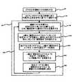
複数のピクセルを持つ表示アレイに対するリアルタイム校正スケジューリングを詳細に説明する。図1は、本発明の一実施例による校正スケジューリングのための処理を図示している。この技術によれば、ピクセルは当該表示アレイの通常の動作の間における、斯かるピクセルの経時変化(aging)及び/又は使用に基づいて校正される。 The real-time calibration scheduling for a display array with multiple pixels is described in detail. FIG. 1 illustrates a process for calibration scheduling according to one embodiment of the present invention. According to this technique, pixels are calibrated based on the aging and / or use of such pixels during normal operation of the display array.
ピクセルの連結リスト(linked list)がステップS2において発生される。該連結リストは、校正のための高輝度を持つピクセルの識別子を含む。該連結リストは、校正の優先度をスケジュールするために使用される。 A linked list of pixels is generated in step S2. The linked list includes identifiers of pixels with high brightness for calibration. The linked list is used to schedule calibration priorities.
ステップS4において、“n”が表示器のサイズ及び時間に伴う予測される非安定性(例えば、トランジスタ及び発光デバイスの特性のずれ)に基づいて選択される。“n”は、各プログラミングサイクルにおいて校正されるピクセルの数を表す。“n”は1又は2以上とすることができる。 In step S4, “n” is selected based on the expected instability with the size and time of the display (eg, transistor and light emitting device characteristic shifts). “N” represents the number of pixels calibrated in each programming cycle. “N” may be 1 or 2 or more.
次いで、ステップS6においてプログラミングサイクルが開始する。ステップS6は、ステップS8〜S16を含む。ステップS8〜S16は、当該表示アレイの選択された列に対して実施される。 Next, the programming cycle starts in step S6. Step S6 includes steps S8 to S16. Steps S8-S16 are performed on the selected column of the display array.
ステップS8において、選択された列における“n”個のピクセルが、前記連結リストの始めから選択される(以下、“選択ピクセル”と称す)。 In step S8, “n” pixels in the selected column are selected from the beginning of the linked list (hereinafter referred to as “selected pixels”).
ステップS10において、上記選択ピクセルに対して“校正モード”が可能に(イネーブルされる一方、当該表示アレイの選択された列におけるピクセルの残りに対しては“通常動作モード”が可能にされる。 In step S10, a “calibration mode” is enabled for the selected pixel (while enabled, while a “normal operation mode” is enabled for the rest of the pixels in the selected column of the display array.
ステップS12において、選択された列における全ピクセルが、当該ピクセルのデータラインに接続された電圧源ドライバ(例えば、図2の28)によりプログラムされる。 In step S12, all pixels in the selected column are programmed by a voltage source driver (eg, 28 in FIG. 2) connected to the data line for that pixel.
前記選択ピクセルに関し、プログラミングサイクルの間においてデータラインを介して流れる電流がモニタリングされる。該選択された列における上記選択ピクセル以外のピクセルに関しては、対応するプログラミング電圧がメモり(例えば、図2の34、以下“ΔV補償メモリ”と称す)に記憶されたデータを用いて上昇(ブースト)される。 For the selected pixel, the current flowing through the data line during the programming cycle is monitored. For pixels other than the selected pixel in the selected column, the corresponding programming voltage is raised (boosted) using data stored in memory (eg, 34 in FIG. 2, hereinafter referred to as “ΔV compensation memory”). )
ステップS14において、上記のモニタリングされた電流は、データラインを介して流れるべき期待された電流と比較される。次いで、前記選択ピクセルに関する校正データ曲線が発生される。該校正データ曲線に基づいてΔV補償メモリが更新される。 In step S14, the monitored current is compared with the expected current to flow through the data line. A calibration data curve for the selected pixel is then generated. The ΔV compensation memory is updated based on the calibration data curve.
ピクセルに関してΔV補償メモリに記憶された校正データ曲線は、該ピクセルが通常動作モードである場合の次のプログラミングサイクルにおいて該ピクセルに対するプログラミング電圧をブーストするために使用されるであろう。 The calibration data curve stored in the ΔV compensation memory for the pixel will be used to boost the programming voltage for the pixel in the next programming cycle when the pixel is in normal operating mode.
ステップS16において、上記の選択ピクセルの識別子が前記連結リストの終端部に送られる。これら選択ピクセルは、校正に関して該連結リストにおいて最低の優先度を有する。 In step S16, the identifier of the selected pixel is sent to the end of the linked list. These selected pixels have the lowest priority in the linked list for calibration.
表示動作(S6〜S16)の間において、上記連結リストは、校正されるべきピクセルの並び替えられた優先リストを提供する。本説明において、“連結リスト”なる用語及び“優先リスト”なる用語は入れ替え可能に使用され得ることに注意されたい。 During the display operation (S6-S16), the linked list provides a sorted priority list of pixels to be calibrated. Note that in this description, the terms “linked list” and “priority list” may be used interchangeably.
当該動作はステップS8に戻る(S18)。そして、次のプログラミングサイクルが開始する。当該表示アレイにおける新たな列が活性化され(選択され)、該新たに活性化された列における新たな“n”個のピクセルが上記連結リストの先頭から選択される。該新たな選択ピクセルに関して得られた校正データを用いて、ΔV補償メモリが更新される。 The operation returns to step S8 (S18). Then, the next programming cycle starts. A new column in the display array is activated (selected), and new “n” pixels in the newly activated column are selected from the top of the linked list. The ΔV compensation memory is updated with the calibration data obtained for the new selected pixel.
次に、上記選択ピクセルの数“n”を詳細に説明する。上述したように、数“n”は、表示器のサイズ及び時間に伴うデバイス特性の予測される非安定性に基づいて決定される。ピクセルの総数NはN=3xm1xm2であると仮定し、ここでm1及びm2は、各々、当該表示器における行及び列の数である。Next, the number “n” of the selected pixels will be described in detail. As described above, the number “n” is determined based on the expected instability of the device characteristics with size and time of the display. The total number of pixels N is assumed to beN =
特性ずれの最高の率はK(=ΔI/Δt・I)である。各プログラミングサイクルはt=1/f・m2掛かる。表示器全体が校正された後の最大の予測される特性のずれは、ΔI/I=K・t・N/n<eであり、ここで、eは許容される誤差である。この後、校正は始めから再実行することができ、誤差が除去される。これは、n>K・t・N/e又はn>3・K・m1/f・eであることを示す。例えば、K=1%/hr、m1=1024、f=60Hz、及びe=0.1%であるなら、n>0.14であり、これは5プログラミングサイクルに1回校正する必要があることを意味する。これは、5プログラミングサイクルに1回動作するような1つの校正ユニットにより達成可能である。各校正ユニットは、プログラミングサイクルにおいて1つのピクセルの校正を可能にする。e=0.01%なら、n>1.4である。これは、各プログラミングサイクルにおいて2つのピクセルを校正する2つの校正ユニットが必要となることを意味する。これは、この校正システムを非常に低コストで実施化することができることを示している。The highest rate of characteristic deviation is K (= ΔI / Δt · I). Each programming cycle takes t = 1 / f · m2 . The largest expected characteristic deviation after the entire display is calibrated is ΔI / I = K · t · N / n <e, where e is an acceptable error. After this, the calibration can be re-executed from the beginning and the error is removed. This indicates that n> K · t · N / e or n> 3 · K · m1 / f · e. For example, if K = 1% / hr, m1 = 1024, f = 60 Hz, and e = 0.1%, then n> 0.14, which needs to be calibrated once every 5 programming cycles. Means that. This can be achieved with one calibration unit that operates once every five programming cycles. Each calibration unit allows calibration of one pixel in the programming cycle. If e = 0.01%, n> 1.4. This means that two calibration units are needed to calibrate two pixels in each programming cycle. This shows that this calibration system can be implemented at a very low cost.
表示器は時を経るほど、校正の頻度は自動的に低下され得る。何故なら、特性のずれは時間が経過するにつれて一層遅くなるからである。加えて、校正のために選択されるピクセルは、表示データに依存する異なる電流でプログラムすることができる。唯一の条件は、それらのプログラミング電流が基準電流より大きいということである。したがって、一層高い精度を達成するために、校正は1つのピクセルに対して複数輝度レベルで実行することができる。 As time passes, the frequency of calibration can be automatically reduced. This is because the characteristic deviation becomes slower as time elapses. In addition, the pixels selected for calibration can be programmed with different currents depending on the display data. The only requirement is that their programming current is greater than the reference current. Thus, to achieve higher accuracy, calibration can be performed on multiple brightness levels for one pixel.
次に、連結リストを詳細に説明する。連結リストには、校正のための高輝度を持つピクセルが掲載される。表示データは、斯かる校正のための高輝度を持つピクセルを決定するために使用される。低電流における校正は遅く、時には正確でない。加えて、最大の特定のずれは、高電流のピクセルに対して発生する。このように、精度及び校正速度を改善するために、閾電流ITHより大きな電流でプログラムされるべきピクセルが選択され、連結リストに記憶される。Next, the linked list will be described in detail. The linked list contains pixels with high brightness for proofreading. The display data is used to determine pixels with high brightness for such calibration. Calibration at low currents is slow and sometimes not accurate. In addition, the largest specific deviation occurs for high current pixels. Thus, to improve accuracy and calibration speed, pixels to be programmed with a current greater than the threshold current ITH are selected and stored in the linked list.
ITHは変数であり、“0”であり得る。ITH=0の場合は、全ピクセルが連結リストに掲載され、校正は、それらのプログラミング電流に関係なく全てのピクセルに対して実行される。ITH is a variable and can be “0”. If ITH = 0, all pixels are listed in the linked list and calibration is performed on all pixels regardless of their programming current.
前述した校正−スケジューリング技術は、限定されるものではないが、例えばカレントミラー型ピクセル等の如何なる電流プログラム型ピクセルにも適用可能である。 The calibration-scheduling technique described above is applicable to any current-programmed pixel, such as, but not limited to, a current mirror pixel.
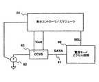
図2は、図1の校正−スケジューリング法を実施するためのシステム構成の一例を図示している。校正−スケジューリングアルゴリズムを実施するための図2のシステム30は、複数のピクセル回路12を持つ表示アレイ10に対して設けられている。ピクセル回路12は、限定されるものではないがカレントミラー型ピクセル等の電流プログラム型ピクセル回路である。ピクセル回路12は、行及び列に配列されている。 FIG. 2 shows an example of a system configuration for implementing the calibration-scheduling method of FIG. The system 30 of FIG. 2 for implementing a calibration-scheduling algorithm is provided for a
ピクセル回路12は、OLED及び複数のトランジスタ(例えば、TFT)を含むことができる。該トランジスタは、アモルファスシリコン、ナノ/マイクロ結晶シリコン、ポリシリコン、有機半導体技術(例えば、有機TFT)、NMOS/PMOS技術又はCMOS技術(例えば、MOSFET)を用いて作製することができる。表示アレイ10は、AMOLED表示アレイとすることができる。 The
ピクセル回路12は、ゲートドライバ20に接続されたゲートライン14、電圧データドライバ28に接続されたデータライン16、及び電源24に接続された電源ライン18により動作される。図2においては、2つのデータライン、2つのゲートライン及び2つの電源ラインが一例として示されている。表示アレイ10に、3つ以上のデータライン、3つ以上のゲートライン及び3つ以上の電源ラインを設けることもできることは明らかである。 The
システム30は、表示アレイ10のプログラミング及び校正を制御するための校正スケジューラ及びメモリブロック32、及びΔV補償電圧(値)を記憶するためのΔV補償メモリ34を含む。各プログラミングサイクルにおいて、表示アレイ10の或る列が選択される。該プログラミングサイクルの間において、校正スケジューラ及びメモリブロック32は、該選択された列(即ち、データライン)に対して通常動作モード又は校正モードをイネーブルする。 The system 30 includes a calibration scheduler and memory block 32 for controlling programming and calibration of the
システム30は、ピクセル電流をモニタリング及び測定するモニタシステムを更に含んでいる。該モニタシステムは、スイッチ36及び38並びに正確な抵抗42を備えるセンサ40を含んでいる。図2において、スイッチ36及び38は、一例として各データラインに設けられている。 The system 30 further includes a monitoring system that monitors and measures the pixel current. The monitoring system includes a
システム30は、上記のモニタリング結果に基づいてΔV補償電圧を発生する発生器を更に含んでいる。該発生器は、アナログ/デジタル変換器(A/D)44、比較器46及びトランスレータ48を含んでいる。A/D44は、電圧センサ40の出力をデジタル出力に変換する。比較器46は、該デジタル出力をトランスレータ48の出力と比較する。トランスレータ48は、デジタルデータ入力52に対して関数f(V)を実行する。トランスレータ48は、f(V)を介して電流データ入力52を電圧データ入力に変換する。比較器46による比較の結果は、ΔV補償メモリ34に記憶される。 The system 30 further includes a generator that generates a ΔV compensation voltage based on the monitoring result. The generator includes an analog / digital converter (A / D) 44, a
システム30は、デジタルデータ入力52と、ΔV補償メモリ34に記憶されたΔV補償電圧とを加算する加算器50を更に含んでいる。電圧データドライバ28は、データラインを加算器50の出力に基づいて駆動する。かくして、データライン用のプログラミングデータは、上記ΔV電圧を加算することにより調整される。 The system 30 further includes an adder 50 that adds the digital data input 52 and the ΔV compensation voltage stored in the ΔV compensation memory 34. The voltage data driver 28 drives the data line based on the output of the adder 50. Thus, the programming data for the data line is adjusted by adding the ΔV voltage.
前記校正スケジューラ及びメモリブロック32が、選択されたデータラインに対して通常動作モードをイネーブルする場合、スイッチ36が作動される。かくして、電圧データドライバ28の電圧出力は当該データライン上のピクセルに直接供給される。 When the calibration scheduler and memory block 32 enables the normal mode of operation for the selected data line, the
校正スケジューラ及びメモリブロック32が当該データラインに対して校正モードをイネーブルすると、スイッチ38が作動される。かくして、電圧は正確な抵抗42を介して当該データライン上のピクセルに供給される。プログラミングサイクルの最終段階における(即ち、初期過渡状態が完了した場合の)抵抗42の両端間の電圧降下が電圧センサ40により測定される。電圧センサ40によりモニタリングされた電圧降下は、A/D44によりデジタルデータに変換される。上記電圧降下の結果的値は、当該ピクセルが電流プログラム型ピクセル回路である場合、該ピクセルを介して流れる電流に比例する。この値は、比較器46により、トランスレータ48により得られる期待された値と比較される。 When the calibration scheduler and memory block 32 enable the calibration mode for the data line, switch 38 is activated. Thus, the voltage is supplied to the pixel on the data line via a precise resistor 42. The voltage drop across the resistor 42 is measured by the
期待された値と測定された値との間の差は、ΔV補償メモリ34に記憶され、後のプログラミングサイクルに対して使用される。上記差は、将来において当該ピクセルのプログラミングに対するデータ電圧を調整するために使用される。 The difference between the expected value and the measured value is stored in the ΔV compensation memory 34 and used for subsequent programming cycles. The difference is used in the future to adjust the data voltage for programming the pixel.
校正スケジューラ及びメモリブロック32は、前述した連結リストを含むことができる。開始時に、該連結リストは自動的に発生される。該リストは、ピクセルの単なるリストであり得る。しかしながら、動作中に該リストは修正される。 The calibration scheduler and memory block 32 may include the linked list described above. At the start, the linked list is automatically generated. The list can be just a list of pixels. However, the list is modified during operation.
高輝度を持つピクセル回路の校正は、大又は小面積表示器において必要とされる高速且つ正確な校正を保証する。 Calibration of pixel circuits with high brightness ensures the fast and accurate calibration required in large or small area displays.
表示アレイ10は電圧プログラミング技術を用いて駆動されるので、当該校正は高速であり、高解像度及び大面積表示器に使用することができる。 Since the
実施化の速度、精度及び容易さにより、当該校正−スケジューリング技術の応用は、携帯電話、パーソナルオーガナイザ、モニタ、TVに使用されるエレクトロルミネッセント装置から大面積表示器ボードまでにわたる。 Depending on the speed, accuracy and ease of implementation, the application of the calibration-scheduling technique ranges from electroluminescent devices used in cell phones, personal organizers, monitors, TVs to large area display boards.
システム30は、当該ピクセルの時間依存性パラメータに依存するような電圧降下をモニタリング及び測定し、望ましいプログラミングデータを発生する。しかしながら、ピクセルの時間依存性パラメータは、図2のもの以外の如何なるメカニズムにより抽出することもできる。 System 30 monitors and measures voltage drops as a function of the pixel's time dependent parameters and generates the desired programming data. However, the pixel time-dependent parameters can be extracted by any mechanism other than that of FIG.
プログラミングし、ピクセルの時間依存性パラメータを抽出し、且つ該ピクセルを駆動する他の技術を、図3〜7を参照して詳細に説明する。この技術は、校正のための電圧抽出を含む。プログラミング電圧は該抽出された情報により校正され、結果として、時間にわたり安定したピクセル電流が得られる。この技術を用いて、ピクセルの経時変化が抽出される。 Other techniques for programming, extracting pixel time dependent parameters, and driving the pixels are described in detail with reference to FIGS. This technique includes voltage extraction for calibration. The programming voltage is calibrated with the extracted information, resulting in a stable pixel current over time. Using this technique, pixel aging is extracted.
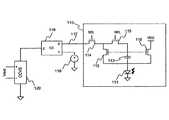
図3は、本発明の一実施例による電圧抽出、プログラミング及び駆動を実施するためのシステムアーキテクチャを図示している。図3のシステムは、電流モードピクセル回路60に対して電圧抽出及びプログラミングを実施する。ピクセル回路60は、発光デバイスと、駆動トランジスタを含む複数のトランジスタとを有している(図示略)。これらトランジスタはTFTとすることができる。 FIG. 3 illustrates a system architecture for performing voltage extraction, programming and driving according to one embodiment of the present invention. The system of FIG. 3 performs voltage extraction and programming for the current mode pixel circuit 60. The pixel circuit 60 includes a light emitting device and a plurality of transistors including a driving transistor (not shown). These transistors can be TFTs.
ピクセル回路60は、選択ラインSELにより選択され、データライン61上のDATAにより駆動される。電圧源62は、プログラミング電圧VPをピクセル回路60に書き込むために設けられている。正ノード及び負ノードを持つ電流制御型電圧源(CCVS)63は、データライン61上の電流を電圧Vextに変換するために設けられている。表示コントローラ及びスケジューラ64は、ピクセル回路60を動作させる。該表示コントローラ及びスケジューラ64は、CCVS63から出力される抽出された電圧Vextをモニタリングし、次いで電圧源62を制御する。The pixel circuit 60 is selected by the selection line SEL and is driven by DATA on the
CCVS63の抵抗は無視可能である。かくして、データライン61上の電流は、
ILine=Ipixel=β(VP−VT)2 (1)
と書かれ、ここで、ILineはデータライン61上の電流を表し、Ipixelはピクセル電流を表し、VTはピクセル回路60に含まれる駆動トランジスタの閾電圧を表し、βはTFT特性における利得パラメータを表す。The resistance of
I Line = I pixel = β ( V P -V T) 2 (1)
Written as, where, ILine represents the current on the
時間に伴い駆動TFTの閾電圧が増加するにつれて、データライン61上の電流は減少する。抽出された電圧Vextをモニタリングすることにより、表示コントローラ及びスケジューラ64は該閾電圧のずれの量を決定する。As the threshold voltage of the driving TFT increases with time, the current on the
駆動トランジスタの閾電圧VTは、
VT=VP−(ILine/β)0.5 (2)
と計算することができる。The threshold voltage VT of the driving transistor is
VT = VP − (ILine / β)0.5 (2)
And can be calculated.
プログラミング電圧VPは、抽出された情報を用いて修正される。抽出処理は、各フレーム時間の間に1個又は数個のピクセルに対して実行することができる。The programming voltageVP is modified using the extracted information. The extraction process can be performed on one or several pixels during each frame time.
図4は、上部放射型電流セルピクセル回路70と共に採用される、図3の電圧抽出、プログラミング及び駆動のためのシステムの一例を図示している。ピクセル回路70は、OLED71、記憶キャパシタ72、駆動トランジスタ73並びにスイッチトランジスタ74及び75を含んでいる。 FIG. 4 illustrates an example of a system for voltage extraction, programming, and driving of FIG. 3 that is employed with the top-emitting current
トランジスタ73、74及び75は、n型TFTとすることができる。しかしながら、これらトランジスタ73、74及び75はp型トランジスタとすることもできる。該ピクセル回路70に適用される電圧抽出及びプログラミング技術は、p型トランジスタを有するピクセル回路にも適用することができる。 The
駆動トランジスタ73は、スイッチトランジスタ75を介してデータライン76に接続されると共に、OLED71に接続され、且つ、スイッチトランジスタ74を介して記憶キャパシタ72に接続されている。駆動トランジスタ73のゲート端子は、記憶キャパシタ72に接続されている。スイッチトランジスタ74及び75のゲート端子は、選択ラインSELに接続されている。OLED71は電圧供給電極、即ちラインVDDに接続されている。該ピクセル回路70は、選択ラインSELにより選択されると共に、データライン76上のDATAにより駆動される。 The
電流伝達器(CC)77は、X、Y及びZ端子を有し、データライン76上の電流を、これに負荷を掛けることなく抽出するために使用される。電圧源78は、CC77のY端子にプログラミング電圧を供給する。CC77において、X端子は、帰還によりY端子のものと同一の電圧を有するように強制される。また、X端子上の電流は、当該CC77のZ端子に複写される。電流制御型電圧源(CCVS)79は、正ノード及び負ノードを有している。該CCVS79は、CC77のZ端子上の電流を電圧Vextに変換する。The current transmitter (CC) 77 has X, Y and Z terminals and is used to extract the current on the
Vextは図3の表示コントローラ及びスケジューラ64に供給され、そこにおいて、駆動トランジスタ73の閾電圧が抽出される。表示コントローラ及びスケジューラ64は、該抽出された閾電圧に基づいて電圧源78を制御する。Vext is supplied to the display controller and
図5は、底部放射型電流セルピクセル回路80と共に採用される、図3の電圧抽出、プログラミング及び駆動のためのシステムの他の例を図示している。ピクセル回路80は、OLED81、記憶キャパシタ82、駆動トランジスタ83並びにスイッチトランジスタ84及び85を含んでいる。トランジスタ83、84及び85は、n型TFTとすることができる。しかしながら、これらトランジスタ83、84及び85はp型トランジスタとすることもできる。 FIG. 5 illustrates another example of a system for voltage extraction, programming, and driving of FIG. 3 that is employed with a bottom emitting current
駆動トランジスタ83は、スイッチトランジスタ85を介してデータライン86に接続されると共に、OLED81に接続され、且つ、記憶キャパシタ82に接続されている。駆動トランジスタ83のゲート端子は、スイッチトランジスタ84を介して電圧供給ラインVDDに接続されている。スイッチトランジスタ84及び85のゲート端子は、選択ラインSELに接続されている。該ピクセル回路80は、選択ラインSELにより選択されると共に、データライン86上のDATAにより駆動される。 The
電流伝達器(CC)87は、X、Y及びZ端子を有し、データライン86上の電流を、これに負荷を掛けることなく抽出するために使用される。電圧源88は、CC87のY端子に負のプログラミング電圧を供給する。CC87において、X端子は、帰還によりY端子のものと同一の電圧を有するように強制される。また、X端子上の電流は、当該CC87のZ端子に複写される。電流制御型電圧源(CCVS)89は、正ノード及び負ノードを有している。該CCVS89は、CC87のZ端子の電流を電圧Vextに変換する。A current transmitter (CC) 87 has X, Y and Z terminals and is used to extract the current on the
Vextは図3の表示コントローラ及びスケジューラ64に供給され、そこにおいて、駆動トランジスタ83の閾電圧が抽出される。表示コントローラ及びスケジューラ64は、該抽出された閾電圧に基づいて電圧源88を制御する。Vext is supplied to the display controller and
図6は、上部放射型カレントミラーピクセル回路90と共に採用される、図3の電圧抽出、プログラミング及び駆動のためのシステムの他の例を図示している。ピクセル回路90は、OLED91、記憶キャパシタ92、ミラートランジスタ93及び94、並びにスイッチトランジスタ95及び96を含んでいる。トランジスタ93、94、95及び96は、n型TFTとすることができる。しかしながら、これらトランジスタ93、94、95及び96はp型トランジスタとすることもできる。 FIG. 6 illustrates another example of a system for voltage extraction, programming, and driving of FIG. 3 employed with a top-emitting current
ミラートランジスタ93は、スイッチトランジスタ95を介してデータライン97に接続されると共に、スイッチトランジスタ96を介して記憶キャパシタ92に接続されている。ミラートランジスタ93及び94のゲート端子は、記憶キャパシタ92及び及びスイッチトランジスタ96に接続されている。ミラートランジスタ94は、OLED91を介して電圧供給電極、即ちラインVDDに接続されている。スイッチトランジスタ85及び86のゲート端子は、選択ラインSELに接続されている。当該ピクセル回路90は、選択ラインSELにより選択されると共に、データライン97上のDATAにより駆動される。 The
電流伝達器(CC)98は、X、Y及びZ端子を有し、データライン97上の電流を、これに負荷を掛けることなく抽出するために使用される。電圧源99は、CC98のY端子に正のプログラミング電圧を供給する。CC98において、X端子は、帰還によりY端子の電圧と同一の電圧を有するように強制される。また、X端子上の電流は、当該CC98のZ端子に複写される。電流制御型電圧源(CCVS)100は、正ノード及び負ノードを有している。該CCVS100は、CC98のZ端子上の電流を電圧Vextに変換する。A current transmitter (CC) 98 has X, Y and Z terminals and is used to extract the current on the
Vextは図3の表示コントローラ及びスケジューラ64に供給され、そこにおいて、駆動トランジスタ93の閾電圧が抽出される。表示コントローラ及びスケジューラ64は、該抽出された閾電圧に基づいて電圧源99を制御する。Vext is supplied to the display controller and
図7は、底部放射型カレントミラーピクセル回路110と共に採用される、図3の電圧抽出、プログラミング及び駆動のためのシステムの他の例を図示している。ピクセル回路110は、OLED111、記憶キャパシタ112、ミラートランジスタ113及び116、並びにスイッチトランジスタ114及び115を含んでいる。トランジスタ113、114、115及び116は、n型TFTとすることができる。しかしながら、これらトランジスタ113、114、115及び116はp型トランジスタとすることもできる。 FIG. 7 illustrates another example of a system for voltage extraction, programming, and driving of FIG. 3 that is employed with a bottom emitting current
ミラートランジスタ113は、スイッチトランジスタ114を介してデータライン117に接続されると共に、スイッチトランジスタ115を介して記憶キャパシタ112に接続されている。ミラートランジスタ113及び116のゲート端子は、記憶キャパシタ112及び及びスイッチトランジスタ115に接続されている。ミラートランジスタ116は、電圧供給ラインVDDに接続されている。ミラートランジスタ113、116及び記憶キャパシタ112はOLED111に接続されている。スイッチトランジスタ114及び115のゲート端子は、選択ラインSELに接続されている。当該ピクセル回路110は、選択ラインSELにより選択されると共に、データライン117上のDATAにより駆動される。 The
電流伝達器(CC)118は、X、Y及びZ端子を有し、データライン117の電流を、これに負荷を掛けることなく抽出するために使用される。電圧源119は、CC118のY端子に正のプログラミング電圧を供給する。CC118において、X端子は、帰還により該CC118のY端子の電圧と同一の電圧を有するように強制される。また、X端子上の電流は、当該CC118のZ端子に複写される。電流制御型電圧源(CCVS)120は、正ノード及び負ノードを有している。該CCVS120は、CC118のZ端子上の電流を電圧Vextに変換する。The current transmitter (CC) 118 has X, Y and Z terminals and is used to extract the current of the
Vextは図3の表示コントローラ及びスケジューラ64に供給され、そこにおいて、駆動トランジスタ113の閾電圧が抽出される。表示コントローラ及びスケジューラ64は、該抽出された閾電圧に基づいて電圧源119を制御する。Vext is supplied to the display controller and
図3〜7を参照すると、上記電圧抽出技術を用いてピクセルの時間依存性パラメータ(例えば、閾ずれ)を抽出することができる。かくして、プログラミング電圧は上記の抽出された情報を用いて校正することができ、結果として時間にわたり安定したピクセル電流が得られる。OLED(即ち、図4の71、図5の81、図6の91、図7の111)の電圧は電流に直接的に影響を与えるので、上述した電圧抽出駆動技術は、OLEDの劣化及び閾ずれを抽出するために使用することもできる。 Referring to FIGS. 3 to 7, pixel time-dependent parameters (e.g., threshold deviation) can be extracted using the voltage extraction technique. Thus, the programming voltage can be calibrated using the above extracted information, resulting in a stable pixel current over time. Since the voltage of the OLED (
上述した電圧抽出技術は、カレントミラー及び電流セルピクセル回路アーキテクチャを含む如何なる電流モードピクセル回路とでも使用することができ、図2の表示アレイ10に適用することができる。上記の抽出された情報を用いて、長期間の表示動作の下でもピクセルの経時変化に関わりのない安定した電流を供給することができる。このようにして、表示動作寿命が有効に改善される。 The voltage extraction technique described above can be used with any current mode pixel circuit, including current mirror and current cell pixel circuit architecture, and can be applied to the
図3〜7のピクセル回路のトランジスタは、アモルファスシリコン、ナノ/マイクロ結晶シリコン、ポリシリコン、有機半導体技術(例えば、有機TFT)、NMOS/PMOS技術又はCMOS技術(例えば、MOSFET)を用いて作製することができることに注意されたい。また、図3〜7のピクセル回路は、AMOLED表示アレイを形成することができる。 The transistors of the pixel circuit of FIGS. 3-7 are fabricated using amorphous silicon, nano / microcrystalline silicon, polysilicon, organic semiconductor technology (eg, organic TFT), NMOS / PMOS technology or CMOS technology (eg, MOSFET). Note that you can. Also, the pixel circuits of FIGS. 3-7 can form an AMOLED display array.
プログラミングし、ピクセルの時間依存性パラメータを抽出し、該ピクセルを駆動する他の技術を、図8〜17を参照して詳細に説明する。該技術は、ステップ校正駆動技術を含んでいる。該ステップ校正駆動技術においては、ピクセルの経時変化に関する情報(例えば、閾ずれ)が抽出される。該抽出された情報は安定したピクセル電流/輝度(luminance)を発生するために使用される。1ビット抽出技術を用いるにも拘わらず、抽出される経時変化の分解能は表示ドライバにより規定される。また、動的効果が補償される。何故なら、ピクセルの経時変化は、駆動サイクルと類似した動作条件下で抽出されるからである。 Other techniques for programming, extracting pixel time-dependent parameters, and driving the pixels are described in detail with reference to FIGS. The technique includes a step calibration drive technique. In the step calibration driving technique, information (for example, threshold shift) regarding pixel change with time is extracted. The extracted information is used to generate a stable pixel current / luminance. Despite the use of the 1-bit extraction technique, the resolution of the extracted temporal change is defined by the display driver. Also, dynamic effects are compensated. This is because pixel aging is extracted under operating conditions similar to drive cycles.
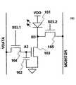
図8は、本発明の一実施例によるステップ校正駆動法が適用されるピクセル回路160を図示している。該ピクセル回路160は、OLED161、記憶キャパシタ162、駆動トランジスタ163、並びにスイッチトランジスタ164及び165を含んでいる。該ピクセル回路160は、電流プログラム型の3TFTピクセル回路である。複数の斯かるピクセル回路160がAMOLED表示器を形成することができる。 FIG. 8 illustrates a
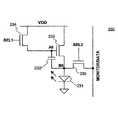
トランジスタ163、164及び165はn型TFTである。しかしながら、トランジスタ163、164及び165はp型TFTとすることもできる。該ピクセル回路160に適用されたステップ校正駆動技術は、p型トランジスタを有するピクセル回路にも適用することができる。トランジスタ163、164及び165はアモルファスシリコン、ナノ/マイクロ結晶シリコン、ポリシリコン、有機半導体技術(例えば、有機TFT)、NMOS/PMOS技術又はCMOS技術(例えば、MOSFET)を用いて作製することができる。
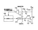
駆動トランジスタ163のゲート端子は、スイッチトランジスタ164を介して信号ラインVDATAに接続されると共に、記憶キャパシタ162にも接続されている。駆動トランジスタ163のソース端子は共通接地点に接続されている。駆動トランジスタ163のドレイン端子は、スイッチトランジスタ165を介してモニタラインMONITORに接続されると共に、OLED161のカソード電極にも接続されている。 The gate terminal of the
スイッチトランジスタ164のゲート端子は選択ラインSEL1に接続されている。該スイッチトランジスタ164のソース端子は、駆動トランジスタ163のゲート端子に接続されると共に、記憶キャパシタ162に接続されている。スイッチトランジスタ164のドレイン端子は、VDATAに接続されている。 The gate terminal of the
スイッチトランジスタ165のゲート端子は、選択ラインSEL2に接続されている。該スイッチトランジスタ165のソース端子は、MONITORに接続されている。該スイッチトランジスタ165のドレイン端子は、駆動トランジスタ163のドレイン端子に接続されると共に、OLED161のカソード電極に接続されている。該OLED161のアノード電極は、電圧供給電極、即ちラインVDDに接続されている。 The gate terminal of the
トランジスタ163及び164並びに記憶キャパシタ162は、ノードA3で接続されている。トランジスタ163及び165並びにOLED161は、ノードB3において接続されている。
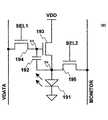
図9は、ドライバ及び抽出ブロック170の一例を、図8の駆動トランジスタ163と共に示す。図9において、RS171a及びRS171bの各々は、前記スイッチトランジスタ(例えば、図8の164、165)のオン抵抗を表している。CSは当該ピクセルの記憶キャパシタを表し、COLEDはOLEDの容量を表し、CPはラインの寄生容量を表している。図9において、OLEDは容量として提示されている。FIG. 9 shows an example of the driver and extraction block 170 together with the
ブロック173は、抽出サイクルの間において駆動トランジスタの閾電圧を抽出するために使用される。ブロック173は、電流感知増幅器(SA)又は電流比較器とすることができる。本説明において、ブロック173は“SAブロック173”と称する。
MONITORラインの電流が基準電流(IREF)より大きい場合、SAブロック173の出力(即ち、図10、11のトリガ(Trigger))は“1”となる。MONITORラインの電流が基準電流(IREF)より小さい場合、SAブロック173の出力は“0”となる。 When the current of the MONITOR line is larger than the reference current (IREF), the output of the SA block 173 (that is, the trigger (Trigger) in FIGS. 10 and 11) becomes “1”. When the current of the MONITOR line is smaller than the reference current (IREF), the output of the SA block 173 is “0”.
SAブロック173は数個の列の間で共有することができ、結果としてオーバーヘッドが小さくなることに注意されたい。また、当該ピクセル回路の校正は1度に1回実行することができ、従って、抽出回路は全ての列の間で共有することができる。 Note that SA block 173 can be shared between several columns, resulting in less overhead. Also, the calibration of the pixel circuit can be performed once at a time, so that the extraction circuit can be shared between all columns.
データ処理ユニット(DPU)ブロック172は、プログラミングサイクル、コントラスト及び輝度を制御し、校正処理を実行し、並びに駆動サイクルを制御するために設けられている。DPUブロック172は、抽出アルゴリズムを実行して駆動トランジスタの閾電圧をSAブロック173からの出力に基づいて抽出(推定)すると共に、駆動トランジスタ163に接続されたドライバ174を制御する。 A data processing unit (DPU) block 172 is provided to control programming cycles, contrast and brightness, perform calibration processing, and control drive cycles. The
図10は、図9のDPUブロック172により実行される抽出アルゴリズムの一例を示してる。図10のアルゴリズムは、DPUブロック172の一部に存する。図10において、VT(i,j)は前の抽出サイクルにおけるピクセル(i,j)の抽出された閾電圧を表し、VSはドライバ174の分解能を表し、“i”はピクセルアレイの行を表し、“j”はピクセルアレイの列を表す。トリガ(Trigger)は、図9のSAブロック173の比較結果を伝える。Less_state180は当該ピクセルの実際のVTが予測されたVT(VTM)より小さい状態を決定し、Equal_state181は当該ピクセルの予測されたVT(VTM)と実際のVTとが等しい状態を決定し、Greater_state182は当該ピクセルの実際のVTが予測されたVT(VTM)より大きい状態を決定する。FIG. 10 shows an example of the extraction algorithm executed by the DPU block 172 of FIG. The algorithm of FIG. 10 resides in part of the
図9のDPU172は中間閾電圧VTMを下記のように決定する:
(A1)s(i,j)=Less_state180の場合、実際の閾電圧はVT(i,j)より小さく、VTMは(VT(i,j)−VS)に設定される。
(A2)s(i,j)=Equal_state181の場合、実際の閾電圧はVT(i,j)に等しく、VTMはVT(i,j)に設定される。
(A3)s(i,j)=Greater_state182の場合、実際の閾電圧はVT(i,j)より大きく、VTMは(VT(i,j)+VS)に設定される。
ここで、s(i,j)は校正メモリ(例えば、図16の208)に記憶されたピクセル(i,j)の前の状態を表す。The
(A1) When s (i, j) =
(A2) When s (i, j) =
(A3) When s (i, j) =
Here, s (i, j) represents the previous state of pixel (i, j) stored in the calibration memory (for example, 208 in FIG. 16).
図11は、図9のDPUブロック172により実行される抽出アルゴリズムの他の例を示している。図11のアルゴリズムは、図9のDPUブロック172の一部に存する。図11において、VT(i,j)は前の抽出サイクルにおけるピクセル(i,j)の抽出された閾電圧を表し、VSはドライバ174の分解能を表し、“i”はピクセルアレイの行を表し、“j”はピクセルアレイの列を表す。トリガ(Trigger)は、SAブロック173の比較結果を伝える。FIG. 11 shows another example of the extraction algorithm executed by the DPU block 172 of FIG. The algorithm of FIG. 11 resides in part of the DPU block 172 of FIG. In FIG. 11, VT (i, j) represents the extracted threshold voltage of pixel (i, j) in the previous extraction cycle, VS represents the resolution of
更に、図11において、Vresは当該ピクセルの実際のVTを得るために、予測されたVT(VTM)に対して加算/減算されるステップを表し、Aは予測ステップの減少利得を表し、Kは予測ステップの増加利得を表す。Further, in FIG. 11, Vres represents a step that is added / subtracted to the predicted VT (VTM ) to obtain the actual VT of the pixel, and A represents the decrease gain of the prediction step. And K represents the increase gain of the prediction step.
図11の動作は、急激な変化の高速抽出のための利得の追加状態L2及びG2を有することを除いて、図10のものと同一である。各利得状態において、変化に一層迅速に追従するためにステップサイズが増加される。L1及びG1は、VT変化が急激であるか又は普通であるかを規定する移行状態である。The operation of FIG. 11 is the same as that of FIG. 10 except that it has additional gain states L2 and G2 for fast extraction of sudden changes. At each gain state, the step size is increased to follow the change more quickly. L1 and G1 are transition conditions specified whether VT change is or is rapidly usual.
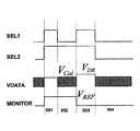
図12は、図8のピクセル回路160に適用される波形の一例を示している。図12において、VCal=VB+VTM、及びVDR=VP+VT(i,j)+VREFであり、ここで、VBは抽出サイクルの間におけるバイアス電圧を表し、VTMは図10又は11に示されるアルゴリズムに基づいて定義され、VPはプログラミング電圧を表し、VT(i,j)は前の抽出サイクルにおける抽出された閾電圧を表し、VREFはプログラミングサイクルの間における駆動トランジスタのソース電圧を表す。FIG. 12 shows an example of a waveform applied to the
図8〜12を参照すると、ピクセル回路160の動作は、動作サイクルX51、X52、X53及びX54を含んでいる。図12において、抽出サイクルはプログラミングサイクルから分離されている。抽出サイクルはX51及びX52を含み、プログラミングサイクルはX53を含む。X54は駆動サイクルである。プログラミングサイクルの終わりにおいて、ノードA3は(VP+VT)に充電され、ここで、VPはプログラミング電圧であり、VTは駆動トランジスタ163の閾電圧である。With reference to FIGS. 8-12, the operation of the
第1動作サイクルX51において:SEL1及びSEL2はハイとなる。ノードA3はVCalに充電され、ノードB3はVREFに充電される。VCalはVB+VTMであり、この場合、VBはバイアス電圧であり、VTMは予測されたVTであり、VREFはVDD−VOLEDOより大きくなければならず、ここでVOLEDOはOLED161のオン電圧である。In the first operating cycle X51: SEL1 and SEL2 go high. Node A3 is charged to VCal, node B3 is charged to VREF. VCal isV B+ V TM, in this case,V B is the biasvoltage, V TM is predictedV T, VREF should be greater thanV DD -VOLEDO, where VOLEDO is an on-voltage of the
第2動作サイクルX52において:SEL1はゼロとなる。駆動トランジスタ163のゲート/ソース電圧は、
VGS=VB+VTM+ΔVB+ΔVTM−ΔVT2−ΔVH
により与えられ、ここで、VGSは駆動トランジスタ163のゲート/ソース電圧を表し、ΔVB、ΔVTM、ΔVT2及びΔVHは、各々、VB、VTM、VT2及びVHに依存する動的影響である。VT2はスイッチトランジスタ164の閾電圧を表し、VHはSEL1がゼロになる場合の第2動作サイクルX52の開始時におけるSEL1の電圧の変化を表す。In the second operating cycle X52: SEL1 goes to zero. The gate / source voltage of the driving
VGS = VB + VTM + ΔVB + ΔVTM −ΔVT2 −ΔVH
Where VGS represents the gate / source voltage of
前記SAブロック173はβ(VB)2より大きな電流を感知するように調整されているので、駆動トランジスタ163のゲート/ソース電圧は(VB+VT)より大きくなり、ここで、βは駆動トランジスタ163のI−V特性における利得パラメータである。Since the SA block 173 is adjusted to sense a current larger than β (VB )2 , the gate / source voltage of the driving
結果として、数回の反復の後、ピクセル(i,j)に関するVTM及び抽出された閾電圧VT(i,j)は、
VTM=VT−γ・(VB+VT+VT2−VH)
γ={Cg2/(2・CS)}/{1+Cg2/(2・CS)}
に収束し、ここで、Cg2はスイッチトランジスタ164のゲート容量を表す。As a result, after several iterations, VTM and extracted threshold voltage VT (i, j) for pixel (i, j) are
VTM = VT −γ · (VB + VT + VT2 −VH )
γ = {C g2 / (2 · C S)} / {1 + C g2 / (2 · C S)}
Where Cg2 represents the gate capacitance of the
第3動作サイクルX53において、SEL1はハイとなる。VDATAはVDRとなる。ノードA3は[VP+VT(i,j)−γ(VP−VB)]に充電される。In the third operation cycle X53, SEL1 goes high. VDATA is theV DR. Node A3 is charged to [VP + VT (i, j) −γ (VP −VB )].
第4動作サイクルX54において:SEL1及びSEL2はゼロとなる。前記動的影響を考慮すると、駆動トランジスタ163のゲート/ソース電圧は、
VGS=VP+VT
と書くことができる。In the fourth operating cycle X54: SEL1 and SEL2 are zero. Considering the dynamic influence, the gate / source voltage of the driving
VGS = VP + VT
Can be written.
従って、当該ピクセル電流は、閾電圧ずれの静的及び動的影響から独立したものとなる。 Thus, the pixel current is independent of the static and dynamic effects of threshold voltage deviation.
図12において、抽出サイクル及びプログラミングサイクルは別のサイクルとして示されている。しかしながら、抽出サイクル及びプログラミングサイクルは図13に示すように併合することもできる。図13は、図8のピクセル回路160に適用される波形の他の例を示している。 In FIG. 12, the extraction cycle and the programming cycle are shown as separate cycles. However, the extraction cycle and the programming cycle can also be merged as shown in FIG. FIG. 13 shows another example of a waveform applied to the
図8〜11及び13を参照すると、ピクセル回路160の動作は動作サイクルX61、X62及びX63を含んでいる。プログラミング及び抽出サイクルは、動作サイクルX61及びX62に併合されている。動作サイクルX63は、駆動サイクルである。 With reference to FIGS. 8-11 and 13, the operation of the
プログラミングサイクルの間において、ピクセル電流は所望の電流と比較され、駆動トランジスタの閾電圧が図10又は11のアルゴリズムを用いて抽出される。ピクセル回路160は、動作サイクルX61の間においてVDR=VP+VT(i,j)+VREFによりプログラムされる。次いで、ピクセル電流はMONITORラインを介してモニタリングされ、所望の電流と比較される。該比較結果に基づくと共に、図10又は11の抽出アルゴリズムを使用して、閾電圧VT(i,j)が更新される。During the programming cycle, the pixel current is compared with the desired current and the threshold voltage of the drive transistor is extracted using the algorithm of FIG.
図8には、2つの選択ラインSEL1及びSEL2が示されている。しかしながら、スイッチトランジスタ164及び165を動作させるために、信号選択ライン(例えば、SEL1)を共通の選択ラインとして使用することもできる。共通の選択ラインを使用する場合、図12のSEL1は第2動作サイクルX52においてハイに留まり、VGSは(VB+VTM)に留まる。従って、前記動的影響は検出されない。FIG. 8 shows two selection lines SEL1 and SEL2. However, the signal select line (eg, SEL1) can also be used as a common select line to operate the
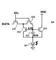
上述したステップ校正駆動技術は、図14のピクセル回路190にも適用可能である。該ピクセル回路190は、OLED191、記憶キャパシタ192、駆動トランジスタ193、並びにスイッチトランジスタ194及び195を含んでいる。該ピクセル回路190は、電流プログラム型の3TFTピクセル回路である。複数の斯かるピクセル回路190がAMOLED表示器を形成することができる。 The step calibration driving technique described above can also be applied to the
トランジスタ193、194及び195はn型TFTである。しかしながら、トランジスタ193、194及び195はp型TFTとすることもできる。該ピクセル回路190に適用されたステップ校正駆動技術は、p型トランジスタを有するピクセル回路にも適用することができる。トランジスタ193、194及び195はアモルファスシリコン、ナノ/マイクロ結晶シリコン、ポリシリコン、有機半導体技術(例えば、有機TFT)、NMOS/PMOS技術又はCMOS技術(例えば、MOSFET)を用いて作製することができる。
駆動トランジスタ193のゲート端子は、スイッチトランジスタ194を介して信号ラインVDATAに接続されると共に、記憶キャパシタ192にも接続されている。駆動トランジスタ193のソース端子は、OLED191のアノード電極に接続されると共に、スイッチトランジスタ195を介してモニタラインMONITORに接続されている。駆動トランジスタ193のドレイン端子は、電圧供給ラインVDDに接続されている。トランジスタ194及び195のゲート端子は選択ラインSEL1及びSEL2に各々接続されている。 The gate terminal of the
トランジスタ193及び194並びに記憶キャパシタ192は、ノードA4で接続されている。トランジスタ195、OLED191及び記憶キャパシタ192は、ノードB4において接続されている。
該ピクセル回路190の構成は、OLED191が駆動トランジスタ193のソース端子にあることを除き、図8のものと類似している。該ピクセル回路190の動作は、図12又は13のものと同様である。 The configuration of the
駆動TFT193のソース端子は抽出サイクル(X51及びX52又はX62)の間においてVREFに強制されるので、抽出されるデータは接地点跳ね返り(ground
bouncing)とは無関係となる。また、プログラミングサイクル(X53又はX61)の間において、駆動TFTのソース端子はVREFに強制されるので、該駆動TFTのゲート/ソース電圧は接地点跳ね返りとは無関係となる。これらの状況の結果、当該ピクセル電流は接地点跳ね返りとは無関係となる。Since the source terminal of the
bouncing). Also, during the programming cycle (X53 or X61), the source terminal of the drive TFT is forced to VREF , so the gate / source voltage of the drive TFT is independent of ground bounce. As a result of these situations, the pixel current is independent of ground bounce.
図15は、ステップ校正駆動技術に対するシミュレーションの結果を示している。図15において、“ケースI”は、第2動作サイクル(図12のX52)においてSEL1がゼロになる場合の図8の動作を表している。“ケースII”は、第2動作サイクルにおいてSEL1がハイに留まる場合の図8の動作を表している。 FIG. 15 shows simulation results for the step calibration drive technique. In FIG. 15, “Case I” represents the operation of FIG. 8 when SEL1 becomes zero in the second operation cycle (X52 of FIG. 12). “Case II” represents the operation of FIG. 8 when SEL1 remains high in the second operation cycle.
図15において、ΔVTRは駆動トランジスタ(例えば、図8の163)の閾電圧の最小の検出可能なずれであり、ΔVT2Rはスイッチトランジスタ(例えば、図8の164)の閾電圧の最小の検出可能なずれであり、IPLは駆動サイクルの間における当該ピクセルのピクセル電流である。In FIG. 15, ΔVTR is the minimum detectable shift in the threshold voltage of the drive transistor (eg, 163 in FIG. 8), and ΔVT2R is the minimum detection of the threshold voltage in the switch transistor (eg, 164 in FIG. 8). A possible deviation,IPL is the pixel current of the pixel during the drive cycle.
所与のプログラミング電圧に対してケースIIのピクセル電流は、閾電圧のずれの動的影響により、ケースIのものより小さい。また、ケースIIのピクセル電流は駆動トランジスタの閾電圧が増加するにつれて増加し(a)、スイッチトランジスタの閾電圧が減少するにつれて減少する(b)。しかしながら、ケースIのピクセル電流は安定している。ピクセル電流に誘起される最大のエラーは、駆動及びスイッチTFTの閾電圧の如何なるずれに対しても0.5%未満である。ピクセル電流に対するVTのずれの影響が支配的であるので、ΔVT2RがΔVTRより大きいのは明である。これらの2つのパラメータは、ドライバ(例えば、図9の174)の分解能(VS)及びSAブロック(例えば、図9の193)のSNRにより制御される。ΔVTRより小さなずれは検出することができず、且つ、閾ずれの時定数は大きいので、抽出サイクル(例えば、図12のX51、X52)は、数フレームからなる長い期間の後に実行することができ、結果として電力消費が低くなる。また、主要な動作サイクルは、他のプログラミングサイクル(例えば、図12のX53)及び駆動サイクル(例えば、図12のX54)になる。結果として、プログラミング時間は大幅に減少し、高速プログラミングが前提となるような高解像度、大面積のAMOLED表示器を提供するようになる。For a given programming voltage, the Case II pixel current is smaller than that of Case I due to the dynamic effect of threshold voltage shift. In addition, the pixel current in case II increases as the threshold voltage of the driving transistor increases (a) and decreases as the threshold voltage of the switch transistor decreases (b). However, Case I pixel current is stable. The maximum error induced by the pixel current is less than 0.5% for any shift in drive and switch TFT threshold voltages. The influence of the deviation of VT for the pixel current is dominant, the [Delta] VT2R is greater than [Delta] VTR is bright. These two parameters are controlled by the resolution (VS ) of the driver (eg, 174 in FIG. 9) and the SNR of the SA block (eg, 193 in FIG. 9). Small deviations from the [Delta] VTR can not be detected, and, since the time constant is large threshold shift, extraction cycle (e.g., X51 of Figure 12, X52) is to be performed after a long period of time consisting of several frames As a result, power consumption is reduced. The main operation cycle is another programming cycle (for example, X53 in FIG. 12) and a driving cycle (for example, X54 in FIG. 12). As a result, the programming time is greatly reduced, and a high-resolution, large-area AMOLED display that requires high-speed programming is provided.
図16は、表示アレイ200でのステップ校正駆動のためのシステムアーキテクチャの一例を示す。表示アレイ200は複数のピクセル回路(例えば、図8の160又は図14の190)を含む。 FIG. 16 shows an example of a system architecture for step calibration drive in the
表示アレイ200には、ピクセル回路を選択するためのゲートドライバ202、ドライバ/SAブロック204、並びにデータ処理及び校正ユニットブロック206が設けられている。ドライバ/SAブロック204は、図9のドライバ174及びSAブロック173を含んでいる。データ処理及び校正ユニット206は、図9のDPU172を含んでいる。図16における“校正”は、校正メモリ208からの校正データを含むと共に、校正データ処理を設定するための幾つかのユーザ定義定数を含むことができる。“コントラスト”及び“輝度”入力は、ユーザにより当該パネルのコントラスト及び輝度を調整するために使用される。また、“ガンマ補正”データは、OLED特性及び人の目に基づいて定義される。該ガンマ補正入力は、人の目に対してピクセル輝度(luminance)を調整するために使用される。 The
校正メモリ208は、各ピクセルの抽出された閾電圧VT(i,j)及び状態s(i,j)を記憶する。メモリ210は、ガンマ補正、解像度及びコントラスト等を含む表示器の通常の動作のための他の必要なデータを記憶する。DPUブロックは、表示器におけるコントローラ及びスケジューラに割り当てられた通常のタスクを実行する。そのうえ、図10又は11のアルゴリズムが、校正を実行するために該ブロックに追加されている。The
図17は、図16のシステムアーキテクチャに適用される波形の一例を示している。図17において、ROW[1]、ROW[2]及びROW[3]の各々は表示アレイ200の行を表し、“E”は抽出動作を表し、“P”はプログラミング動作を表し、“D”は駆動動作を表している。抽出サイクル(E)は全てのフレームサイクルに対して実行する必要はないことに注意されたい。従って、長い期間(抽出間隔)の後、ピクセルに対して抽出が繰り返される。 FIG. 17 shows an example of waveforms applied to the system architecture of FIG. In FIG. 17, each of ROW [1], ROW [2] and ROW [3] represents a row of the
図17に示されるように、単一の抽出処理のみが、フレームサイクルの間に発生する。また、同一の行のピクセル回路に対するVT抽出は同時に実行される。As shown in FIG. 17, only a single extraction process occurs during the frame cycle. Further, VT extracted for the pixel circuits in the same row are simultaneously executed.
従って、フレームをリフレッシュするのに要する最大時間は、
τF=n・τP+τE
であり、ここで、τFはフレーム時間を表し、τPは記憶キャパシタ(例えば、図8の162)にピクセルデータを書き込むために要する時間を表し、τEは抽出時間を表し、nは当該表示アレイ(例えば、図16の200)における行の数を表す。Therefore, the maximum time required to refresh a frame is
τF = n · τP + τE
Where τF represents the frame time, τP represents the time required to write pixel data to the storage capacitor (eg, 162 in FIG. 8), τE represents the extraction time, and n represents the time Represents the number of rows in the display array (eg, 200 in FIG. 16).
τE=m・τPと仮定すると、フレーム時間τFは、
τF=(n+m)・τP
と書くことができ、ここで、mはプログラミングサイクルタイミング(τP)のスケールにおける抽出サイクルに要するタイミングを表す。Assuming τE = m · τP , the frame time τF is
τF = (n + m) · τP
Where m represents the timing required for the extraction cycle on the scale of the programming cycle timing (τP ).
例えば、60Hzなるフレームレートのクォータ・ビデオ・グラフィックス・アレイ(QVCA)表示器(240x320)に対しては、m=10なら、各行のプログラミング時間は66μsとなり、抽出時間は0.66msとなる。 For example, for a quarter video graphics array (QVCA) display (240 × 320) with a frame rate of 60 Hz, if m = 10, the programming time for each row is 66 μs and the extraction time is 0.66 ms.
上述したステップ校正駆動技術は、図8及び14のもの以外の如何なる電流プログラム型ピクセル回路にも適用可能であることに注意されたい。 Note that the step calibration drive technique described above is applicable to any current-programmed pixel circuit other than that of FIGS.
上記ステップ校正駆動技術を用いて、閾ずれ等の、ピクセルの時間依存性パラメータ(又は複数のパラメータ)が抽出される。次いで、プログラミング電圧が該抽出された情報を用いて校正され、結果として、時間にわたり安定したピクセル電流が得られる。更に、長い表示動作の下でのピクセルの経時変化とは無関係な安定した電流をピクセル回路に供給することができ、これは、表示器動作寿命を効果的に改善する。 Using the above-described step calibration driving technique, a pixel time-dependent parameter (or parameters) such as threshold deviation is extracted. The programming voltage is then calibrated using the extracted information, resulting in a pixel current that is stable over time. Furthermore, a stable current independent of pixel aging under long display operation can be supplied to the pixel circuit, which effectively improves the display operating life.
本発明の他の実施例によるプログラミングし、ピクセルの時間依存性パラメータを抽出し、該ピクセルを駆動する技術を詳細に説明する。該技術はOLED電圧又はOLED電流をモニタリングすることによりピクセルの経時変化に関する情報(例えば、OLED輝度)を抽出し、輝度(luminance)を発生する処理を含む。プログラミング電圧は該抽出された情報を使用して校正され、結果として時間にわたり安定した輝度が得られる。 A technique for programming, extracting a time-dependent parameter of a pixel, and driving the pixel according to another embodiment of the present invention will be described in detail. The technique includes the process of extracting information about pixel aging (eg, OLED luminance) by monitoring OLED voltage or OLED current and generating luminance. The programming voltage is calibrated using the extracted information, resulting in a stable brightness over time.
OLED電圧/電流はOLED(例えば、図8の161、図14の191)における輝度劣化と相関されることが知られているので、一定の輝度を提供するために、プログラミング電圧をOLED電圧/電流により修正することができる。 Since OLED voltage / current is known to correlate with luminance degradation in OLEDs (eg, 161 in FIG. 8, 191 in FIG. 14), the programming voltage can be set to OLED voltage / current to provide constant brightness. Can be corrected.
例えば、駆動サイクルの間において、SEL2がハイの際にOLED(図8の161又は図14の191)の電圧/電流が抽出される。OLED電圧又は電流は該OLEDの輝度劣化に相関されると言われているので、一定の輝度を提供するために、プログラミング電圧を該OLED電圧により修正することができる。 For example, during the drive cycle, the voltage / current of the OLED (161 in FIG. 8 or 191 in FIG. 14) is extracted when SEL2 is high. Since the OLED voltage or current is said to be correlated to the brightness degradation of the OLED, the programming voltage can be modified by the OLED voltage to provide a constant brightness.
図18は、電圧/電流抽出のための波形の一例を示している。図18の波形は、OLED電圧/電流を抽出するために図8のピクセル回路160及び図14のピクセル回路190に適用することができる。図18の動作は、動作サイクルX71、X72及びX73を含んでいる。動作サイクルX71及びX72は、OLED抽出サイクルである。動作サイクルX73は、図12及び13に示した動作サイクルのうちの1つである。 FIG. 18 shows an example of a waveform for voltage / current extraction. The waveform of FIG. 18 can be applied to the
第1動作サイクルX71の間において、SEL1及びSEL2はハイであり、VDATAはゼロである。駆動トランジスタ(図8の163)のゲート/ソース電圧はゼロになる。電流又は電圧が、MONITORラインを介してOLED(図8の161)に供給される。 During the first operating cycle X71, SEL1 and SEL2 are high and VDATA is zero. The gate / source voltage of the driving transistor (163 in FIG. 8) becomes zero. Current or voltage is supplied to the OLED (161 in FIG. 8) via the MONITOR line.
第2動作サイクルX72の間において、SEL2はハイであり、SEL1はローとなる。OLED電圧又は電流が、図10又は11に提示されたアルゴリズムを用いMONITORライを介して抽出される。この波形は如何なる他の駆動波形と組み合わせることもできる。 During the second operating cycle X72, SEL2 is high and SEL1 is low. The OLED voltage or current is extracted via the MONITOR line using the algorithm presented in FIG. This waveform can be combined with any other drive waveform.
上記説明において、図10及び11のアルゴリズムは、経時変化のデータ(即ち、VTずれ)を比較結果(電流と電流との又は電圧と電圧との)に基づいて予測するために使用することができる。しかしながら、図10及び11のアルゴリズムは、VTをVOLEDにより及びOLED電流/電圧の比較結果を基準電流/電圧により置換することによって、OLED電圧VOLEDのずれを予測するために適用することもできる。上記説明においては、図9に示されたシステムアーキテクチャが閾ずれを補償するために使用される。しかしながら、OLEDデータは、図9のアーキテクチャ、即ちDPU172、ブロック173、ドライバ174が使用される場合にも抽出されると理解される。このデータは、OLEDのずれを補償するために使用することができる。In the above description, the algorithm of FIGS. 10 and 11 can be used to predict time-varying data (ie,VT deviation) based on the comparison results (current-to-current or voltage-to-voltage). it can. However, the algorithm of FIG. 10 and 11, by replacing the reference current / voltage comparison result of the VT by VOLED and OLED current / voltage, also be applied to predict the displacement of the OLED voltage VOLED it can. In the above description, the system architecture shown in FIG. 9 is used to compensate for threshold deviation. However, it is understood that OLED data is also extracted when the architecture of FIG. 9, ie,
動作サイクルX73は、プログラミングサイクルを含む如何なる動作サイクルとすることもできる。これは、OLED抽出の後の当該パネルの状態に依存する。それが動作中であるならば、X73は図12及び13における波形のプログラミングサイクルとなる。OLED電圧は、図12/13の駆動サイクルX55/X63の間に抽出することができる。駆動サイクルX55/X63の間の間において、図8又は14のSEL2はハイ電圧となるので、特定のピクセル電流に関してOLEDの電圧をMONITORを介して読み取ることができる。 The operation cycle X73 can be any operation cycle including a programming cycle. This depends on the state of the panel after OLED extraction. If it is in operation, X73 becomes the waveform programming cycle in FIGS. The OLED voltage can be extracted during the drive cycle X55 / X63 of FIG. During the drive cycle X55 / X63, SEL2 in FIG. 8 or 14 is at a high voltage, so that the voltage of the OLED can be read via MONITOR for a specific pixel current.
図19は、電圧/電流抽出のための波形の他の例を示している。図20は、図19の電圧/電流抽出法が適用されるピクセル回路220を示している。 FIG. 19 shows another example of a waveform for voltage / current extraction. FIG. 20 shows a
図20を参照すると、該ピクセル回路220は、OLED221、記憶キャパシタ222、駆動トランジスタ223、並びにスイッチトランジスタ224及び225を含んでいる。複数の斯かるピクセル回路220が、AMOLED表示器を形成することができる。 Referring to FIG. 20, the
トランジスタ223、224及び225はn型TFTである。しかしながら、トランジスタ223、224及び225はp型TFTとすることもできる。該ピクセル回路220に適用される電圧/電流抽出技術は、p型トランジスタを有するピクセル回路にも適用することができる。トランジスタ223、224及び225は、アモルファスシリコン、ナノ/マイクロ結晶シリコン、ポリシリコン、有機半導体技術(例えば、有機TFT)、NMOS/PMOS技術又はCMOS技術(例えば、MOSFET)を用いて作製することができる。
駆動トランジスタ223のゲート端子は、スイッチトランジスタ224のソース端子に接続されると共に、記憶キャパシタ222にも接続されている。駆動トランジスタ223の一方の端子は共通接地点に接続されている。駆動トランジスタ223の他方の端子は、スイッチトランジスタ235を介してモニタ及びデータラインMONITOR/DATAに接続されると共に、OLED221のカソード電極にも接続されている。 The gate terminal of the
スイッチトランジスタ224のゲート端子は選択ラインSEL1に接続されている。該スイッチトランジスタ224の一方の端子は、駆動トランジスタ223のゲート端子に接続されると共に、記憶キャパシタ222に接続されている。該スイッチトランジスタ224の他方の端子は、OLED221のカソード電極に接続されている。 The gate terminal of the
スイッチトランジスタ225のゲート端子は、選択ラインSEL2に接続されている。該スイッチトランジスタ225の一方の端子は、MONITOR/DATAに接続されている。該スイッチトランジスタ225の他方の端子は、駆動トランジスタ223及びOLED221のカソード電極に接続されている。該OLED221のアノード電極は、電圧供給電極、即ちラインVDDに接続されている。 The gate terminal of the
トランジスタ223及び224並びに記憶キャパシタ222は、ノードA5で接続されている。トランジスタ223及び225並びにOLED221は、ノードB5において接続されている。
該ピクセル回路220は、図8のピクセル回路160に類似している。しかしながら、ピクセル回路220においては、MONITOR/DATAラインがモニタリング及びプログラミングの目的のために使用される。 The
図19〜20を参照すると、ピクセル回路220の動作は動作サイクルX81、X82及びX83を含んでいる。 Referring to FIGS. 19-20, the operation of the
第1動作サイクルX81の間において、SEL1及びSEL2はハイとなり、MONITOR/DATAはゼロとなる。駆動トランジスタ(図20の223)のゲート/ソース電圧はゼロとなる。 During the first operating cycle X81, SEL1 and SEL2 are high and MONITOR / DATA is zero. The gate / source voltage of the driving transistor (223 in FIG. 20) becomes zero.
第2動作サイクルX82の間において、電流又は電圧がMONITOR/DATAラインを介してOLEDに供給され、該OLEDの電圧又は電流が抽出される。前述したように、OLED電圧のずれは、該モニタリングされた電圧又は電流に基づき、図10又は11に提示されたアルゴリズムを用いて抽出される。この波形は、如何なる駆動波形とも組み合わせることができる。 During the second operating cycle X82, current or voltage is supplied to the OLED via the MONITOR / DATA line, and the voltage or current of the OLED is extracted. As described above, the OLED voltage deviation is extracted using the algorithm presented in FIG. 10 or 11 based on the monitored voltage or current. This waveform can be combined with any drive waveform.
動作サイクルX83は、プログラミングサイクルを含み如何なる動作サイクルとすることもできる。これは、OLED抽出後の当該パネルの状態に依存する。 The operation cycle X83 can be any operation cycle including a programming cycle. This depends on the state of the panel after OLED extraction.
OLED電圧/電流は、図20のピクセル回路220の駆動サイクルの間において、何れかの駆動技術を用いて一定の電流のためにプログラムされた後に抽出することができる。駆動サイクルの間において、SEL2はハイ電圧となるので、OLEDの電圧は特定のピクセル電流に対してMONITOR/DATAラインを介して読み取ることができる。 The OLED voltage / current can be extracted after being programmed for a constant current using any drive technique during the drive cycle of the
図21は、電圧/電流抽出技術のための波形の他の例を示している。図22は、図21の電圧/電流抽出技術が適用されるピクセル回路230を示している。図21の波形は、OLED電圧/電流を抽出するために図8のピクセル回路160にも適用することができる。 FIG. 21 shows another example of a waveform for the voltage / current extraction technique. FIG. 22 shows a
図22を参照すると、該ピクセル回路230は、OLED231、記憶キャパシタ232、駆動トランジスタ233、並びにスイッチトランジスタ234及び235を含んでいる。複数の斯かるピクセル回路230が、AMOLED表示器を形成することができる。 Referring to FIG. 22, the
トランジスタ233、234及び235はn型TFTである。しかしながら、トランジスタ233、234及び235はp型TFTとすることもできる。該ピクセル回路230に適用される電圧/電流抽出技術は、p型トランジスタを有するピクセル回路にも適用することができる。トランジスタ233、234及び235は、アモルファスシリコン、ナノ/マイクロ結晶シリコン、ポリシリコン、有機半導体技術(例えば、有機TFT)、NMOS/PMOS技術又はCMOS技術(例えば、MOSFET)を用いて作製することができる。
駆動トランジスタ233のゲート端子は、スイッチトランジスタ234のソース端子に接続されると共に、記憶キャパシタ232にも接続されている。該駆動トランジスタ233の一方の端子は電圧供給ラインVDDに接続されている。該駆動トランジスタ233の他方の端子は、スイッチトランジスタ235を介してモニタ及びデータラインMONITOR/DATAに接続されると共に、OLED231のアノード電極にも接続されている。 The gate terminal of the
スイッチトランジスタ234のゲート端子は選択ラインSEL1に接続されている。該スイッチトランジスタ234の一方の端子は、駆動トランジスタ233のゲート端子に接続されると共に、記憶キャパシタ232に接続されている。該スイッチトランジスタ234の他方の端子は、VDDに接続されている。 The gate terminal of the
スイッチトランジスタ225のゲート端子は、選択ラインSEL2に接続されている。該スイッチトランジスタ235の一方の端子は、MONITOR/DATAに接続されている。該スイッチトランジスタ235の他方の端子は、駆動トランジスタ233及びOLED231のアノード電極に接続されている。該OLED231のアノード電極は、VDDに接続されている。 The gate terminal of the
トランジスタ233及び234並びに記憶キャパシタ232は、ノードA6で接続されている。トランジスタ233及び235並びにOLED231は、ノードB5において接続されている。
該ピクセル回路230は、図14のピクセル回路190に類似している。しかしながら、ピクセル回路230においては、MONITOR/DATAラインがモニタリング及びプログラミングの目的のために使用される。 The
図21〜22を参照すると、図22の動作は動作サイクルX91、X92及びX93を含んでいる。 Referring to FIGS. 21-22, the operation of FIG. 22 includes operation cycles X91, X92 and X93.
第1動作サイクルX91の間において、SEL1及びSEL2はハイとなり、VDDはゼロとなる。駆動トランジスタ(図21の233)のゲート/ソース電圧はゼロとなる。 During the first operating cycle X91, SEL1 and SEL2 are high and VDD is zero. The gate / source voltage of the driving transistor (233 in FIG. 21) becomes zero.
第2動作サイクルX92の間において、電流(電圧)がMONITOR/DATAラインを介してOLED(図21の231)に供給され、該OLEDの電圧(電流)が抽出される。前述したように、OLED電圧のずれは、該モニタリングされた電圧又は電流に基づき、図10又は11に提示されたアルゴリズムを用いて抽出される。この波形は、如何なる駆動波形とも組み合わせることができる。 During the second operation cycle X92, current (voltage) is supplied to the OLED (231 in FIG. 21) via the MONITOR / DATA line, and the voltage (current) of the OLED is extracted. As described above, the OLED voltage deviation is extracted using the algorithm presented in FIG. 10 or 11 based on the monitored voltage or current. This waveform can be combined with any drive waveform.
動作サイクルX93は、プログラミングサイクルを含み如何なる動作サイクルとすることもできる。これは、OLED抽出後の当該パネルの状態に依存する。 The operation cycle X93 can be any operation cycle including a programming cycle. This depends on the state of the panel after OLED extraction.
OLED電圧は、図21のピクセル回路230の駆動サイクルの間において、何れかの駆動技術を用いて一定の電流のためにプログラムされた後に抽出することができる。駆動サイクルの間において、SEL2はハイ電圧となるので、OLEDの電圧は特定のピクセル電流に対してMONITOR/DATAラインを介して読み取ることができる。 The OLED voltage can be extracted after being programmed for a constant current using any drive technique during the drive cycle of the
知られているように、OLED特性は負のバイアスストレス下で改善する。結果として、上記OLED電圧/電流から抽出される当該ピクセルのストレス履歴に関係する負のバイアスを、当該表示器が動作していない時間の間において当該OLEDに印加することができる。この方法は、本明細書で提示される如何なるピクセル回路に対しても使用することができる。 As is known, OLED characteristics improve under negative bias stress. As a result, a negative bias related to the stress history of the pixel extracted from the OLED voltage / current can be applied to the OLED during the time that the display is not operating. This method can be used for any pixel circuit presented herein.
前記OLED電圧/電流抽出技術を用いれば、ピクセル回路は、長期間の表示器動作の下でピクセルの経時変化に無関係な安定した輝度を提供することができ、表示器の動作寿命を効果的に改善することができる。 With the OLED voltage / current extraction technique, the pixel circuit can provide stable brightness independent of pixel aging under long-term display operation, effectively increasing the display operating life. Can be improved.
本発明の実施例による発光デバイスを持つ表示アレイにおける不所望な発光(emission)を低減する技術を詳細に説明する。この技術は、プログラムサイクルの間においてプログラミング経路からOLEDを除去する処理を含む。この技術は、ピクセルの正確な経時変化についての情報、例えば駆動トランジスタの実際の閾電圧ずれ/不整合、を抽出するためにハイブリッド駆動技術に採用することができる。発光デバイスは、不所望な発光及びピクセル経時変化に対する発光デバイスの影響を防止するようにプログラミング/校正サイクルの間においてオフされる。この技術は、ポリシリコン、アモルファスシリコン、結晶シリコン及び有機材料を含む如何なる技術で作製される如何なるカレントミラー型ピクセル回路にも適用することができる。 A technique for reducing unwanted emission in a display array having a light emitting device according to an embodiment of the present invention will be described in detail. This technique involves removing the OLED from the programming path during the program cycle. This technique can be employed in hybrid drive techniques to extract information about the exact aging of the pixels, such as the actual threshold voltage shift / mismatch of the drive transistors. The light emitting device is turned off during the programming / calibration cycle to prevent unwanted light emission and the effect of the light emitting device on pixel aging. This technique can be applied to any current mirror type pixel circuit fabricated with any technique including polysilicon, amorphous silicon, crystalline silicon and organic materials.
図23は、プログラミングサイクルの間においてプログラミング経路からOLEDを除去する技術が適用されるミラー型ピクセル回路250を示している。該ピクセル回路250は、OLED251、記憶キャパシタ252、プログラミングトランジスタ253、駆動トランジスタ254並びにスイッチトランジスタ255及び256を含んでいる。トランジスタ253及び254のゲート端子は、スイッチトランジスタ255及び256を介してIDATAに接続されている。 FIG. 23 shows a mirrored
トランジスタ253、254、255及び256は、n型TFTである。しかしながら、トランジスタ253、254、255及び256は、p型TFTとすることもできる。該ピクセル回路250に適用されるOLED除去技術は、p型トランジスタを有するピクセル回路にも適用することができる。トランジスタ253、254、255及び256は、アモルファスシリコン、ナノ/マイクロ結晶シリコン、ポリシリコン、有機半導体技術(例えば、有機TFT)、NMOS/PMOS技術又はCMOS技術(例えば、MOSFET)を用いて作製することができる。 The
トランジスタ253、254及び256並びに記憶キャパシタ252は、ノードA10で接続されている。トランジスタ253及び254、OLED251並びに記憶キャパシタ252は、ノードB10で接続されている。
従来の電流プログラミング法においては、SELがハイとなり、プログラミング電流(IP)がIDATAに供給される。ミラートランジスタ253の幅がミラートランジスタ254の幅より“m”倍大きい場合を考えると、プログラミングサイクルの間にOLED251を介して流れる電流は(M+1)IPとなる。大幅な速度の改善を得るために“m”が大きい場合、不所望な発光がかなりのものとなる。 In conventional current programming methods, SEL goes high and a programming current (IP) is supplied to IDATA. Considering the case where the width of the
対照的に、当該OLED除去技術によれば、VDDは、より低い電圧にされる。このことは、図24に示すようにOLED251がプログラミング経路から除去されるのを保証する。 In contrast, according to the OLED removal technique, VDD is brought to a lower voltage. This ensures that
プログラミングサイクルの間において、SELはハイであり、VDDはOLED251が逆バイアスされるような基準電圧(Vref)となる。従って、OLED251は、該プログラミングサイクルの間において電流経路から除去される。During the programming cycle, SEL is high and VDD is at a reference voltage (Vref ) such that the
プログラミングサイクルの間において、ピクセル回路250は、不所望な発光をすることなく、IDATAを介してスケーリングされた電流によりプログラムすることができる。 During the programming cycle, the
プログラミングサイクルの間において、ピクセル回路250は、電流により且つ前述した技術のうちの1つを用いてプログラムすることができる。駆動トランジスタ254の閾電圧と同一であるミラートランジスタ253の閾電圧を抽出するために、IDATAラインの電圧が読み取られる。 During the programming cycle, the
また、プログラミングサイクルの間において、ピクセル回路250は、IDATAラインを介しての電圧により、前述した技術のうちの1つを用いてプログラムすることができる。駆動トランジスタ254の閾電圧と同一であるミラートランジスタ253の閾電圧を抽出するために、IDATAラインの電流が読み取られる。 Also, during the programming cycle, the
基準電圧Vrefは、ノードB10における電圧がOLED251のオン電圧より小さくなるように選定される。結果として、OLED251はオフし、不所望な発光はゼロとなる。IDATAラインの電圧は、
VP+VT+ΔVT (3)
を含み、ここで、VPは駆動トランジスタ254のドレイン/ソース電圧及びトランジスタ253のゲート/ソース電圧を含み、VTはトランジスタ253(254)の閾電圧であり、ΔVTはVTのずれ/不整合である。The reference voltage Vref is selected so that the voltage at the node B10 is smaller than the ON voltage of the
VP + VT + ΔVT (3)
Includes, where,V P includes a gate / source voltage of the drain / source voltage and the
プログラミングサイクルの終わりにおいて、VDDは自身の元の値になるので、ノードB10における電圧はOLED電圧VOLEDとなる。駆動サイクルにおいて、SELはローとなる。トランジスタ254/253のゲート電圧は定まり、記憶キャパシタ252に記憶される。何故なら、スイッチトランジスタ255及び256はオフとなるからである。従って、駆動サイクルの間におけるピクセル電流は、閾電圧VTとは無関係となる。At the end of the programming cycle, VDD goes to its original value, so the voltage at node B10 becomes the OLED voltage VOLED . In the drive cycle, SEL goes low. The gate voltage of the
当該OLED除去技術は、VTずれ又はVT不整合を抽出するためにハイブリッド駆動技術に採用することができる。(3)から、当該ピクセルが電流によりプログラムされるなら、IDATAラインの電圧における唯一の変化するパラメータはVTずれ/不整合(ΔVT)である。従って、ΔVTを抽出することができ、プログラミングデータをΔVTにより校正することができる。The OLED removing technique can be employed in the hybrid driving technique to extract the VT shift or VT mismatch. (3), if the pixel is programmed by a current, only changing parameters in the voltage of the IDATA line isV T shift / mismatch (.DELTA.VT). Therefore, ΔVT can be extracted, and the programming data can be calibrated by ΔVT.
図25は、上記OLED除去技術を実施化するためのシステムアーキテクチャの一例を示している。表示アレイ260は、複数のピクセル回路(例えば、図23のピクセル回路250)を含む。表示コントローラ及びスケジューラ262は、表示アレイ260の動作を制御及びスケジューリングする。ドライバ264は、当該ピクセル回路に動作電圧を供給する。該ドライバは、当該ピクセル回路に動作電圧を、上記表示コントローラ及びスケジューラ262からの命令/コマンドに基づいて、上述したようにOLEDがプログラミング経路から除去されるように供給する。 FIG. 25 shows an example of a system architecture for implementing the OLED removal technique.
コントローラ及びスケジューラ262は、図3の表示コントローラ及びスケジューラ64の機能を含むことができるか、又は図16のデータ処理及び校正ユニット206の機能を含むことができる。図25のシステムは、これらの機能、前述した校正スケジューリング、前述した電圧/電流抽出、又はこれらの組み合わせの何れかを有することができる。 The controller and
異なるVTに対する、IDATAライン上の電圧に関するシミュレーション結果が図26に示されている。図23〜26を参照すると、IDATAラインの電圧は、トランジスタ253及び254の閾電圧のずれを含んでいる。プログラミング電流は1μAである。For differentV T, the simulation results are shown in Figure 26 with respect to the voltage on IDATA line. Referring to FIGS. 23-26, the voltage on the IDATA line includes a shift in the threshold voltage of
不所望な発光が大幅に低減される結果、解像度が高くなる。また、回路の経時変化及び発光デバイスの経時変化の個々の抽出が可能となり、一層正確な校正が達成される。 Undesirable light emission is greatly reduced, resulting in higher resolution. In addition, it is possible to individually extract the change over time of the circuit and the change over time of the light-emitting device, thereby achieving more accurate calibration.
図4〜8、14、20、21、23及び24に示されたトランジスタの各々は、相補的回路の概念を用いてp型トランジスタと置換することができることに注意されたい。 Note that each of the transistors shown in FIGS. 4-8, 14, 20, 21, 23, and 24 can be replaced with p-type transistors using the concept of complementary circuitry.
また、全ての引用例は参照により本明細書に組み込まれるものとする。 Also, all citations are incorporated herein by reference.
以上、本発明を1以上の実施例に関して説明した。しかしながら、当業者にとり、請求項に記載された本発明の範囲から逸脱することなしに多数の変形及び変更をなすことができることは明らかであろう。 The present invention has been described with reference to one or more embodiments. However, it will be apparent to persons skilled in the art that a number of variations and modifications can be made without departing from the scope of the invention as set forth in the claims.
10 表示アレイ
12、60、70 ピクセル回路
20 ゲートドライバ
24 電源
28 電圧データドライバ
32 校正スケジューラ及びメモリ
34 ΔV補償メモリ
40 電圧センサ
46 比較器
50 加算器
64 表示コントローラ及びスケジューラ
62、78、88、99、119 電圧源
63、79、89、100、120 電流制御型電圧源
77、87、98、118 電流伝達器
71、81、91、111、161 発光デバイス
72、82、92、112、162 記憶キャパシタ
73、83、163 駆動トランジスタ
74、75、84、85、95、96、114、115、164、165 スイッチトランジスタ
93、94、113、116 ミラートランジスタ
172 データ処理ユニット
173 電流感知増幅器又は電流比較器
174 ドライバDESCRIPTION OF
Claims (40)
Translated fromJapanese表示データ及び前の校正データに基づく校正のためのピクセルを優先付けるために使用されるピクセルの優先リストを発生するステップであって、該優先リストが校正のために閾電流より大きな電流でプログラムされる1以上(n個)のピクセルを選択するために使用されるようなステップと、
前記連結リストから、前記表示アレイの選択された列におけるn個のピクセルを選択するステップと、
前記選択された列におけるピクセルに対してプログラミングを実行するステップであって、
前記n個のピクセルに関してピクセル電流をモニタリングすると共に、校正データを得るステップ、
校正のために前記校正データに基づいて補償メモリを更新するステップ、及び
次のプログラミングのために前記優先リストを並び替えるステップ、
を含むようなステップと、
を有する方法。In a method for performing real-time calibration for a display array having a plurality of pixel circuits arranged in rows and columns,
Generating a priority list of pixels used to prioritize pixels for calibration based on display data and previous calibration data, wherein the priority list is programmed with a current greater than a threshold current for calibration. Steps used to select one or more (n) pixels;
Selecting n pixels in a selected column of the display array from the linked list;
Performing programming on pixels in the selected column, comprising:
Monitoring pixel current for the n pixels and obtaining calibration data;
Updating the compensation memory based on the calibration data for calibration, and reordering the priority list for subsequent programming;
Including steps,
Having a method.
前記選択された列における前記n個のピクセルに対して校正モードを可能にすると共に、前記選択された列におけるピクセルの残りに対して通常動作モードを可能にするステップ、
を含むような方法。The method of claim 1, wherein performing the programming comprises:
Enabling a calibration mode for the n pixels in the selected column and enabling a normal operating mode for the rest of the pixels in the selected column;
Including such methods.
校正された前記n個のピクセルを前記優先リストの最後に移動するステップ、
を含むような方法。The method of claim 1, wherein reordering the list comprises:
Moving the calibrated n pixels to the end of the priority list;
Including such methods.
前記電流を感知するステップと、
該電流を期待された電流と比較するステップと、
を含むような方法。The method of claim 1, wherein the monitoring step comprises:
Sensing the current; and
Comparing the current to an expected current;
Including such methods.
前記通常動作モードにおいて前記ピクセルを、前記補償メモリに記憶された校正データとプログラミングデータとの組み合わせに基づいてプログラムするステップ、
を含んでいるような方法。The method of claim 2, wherein performing the programming comprises:
Programming the pixel in the normal mode of operation based on a combination of calibration data and programming data stored in the compensation memory;
Such a way.
該システムは、前記表示アレイのプログラミング及び校正を制御する校正スケジューラを有し、該スケジューラが、
表示データに基づく校正のための1以上のピクセルを掲載する優先リストと、
プログラミングサイクルの間において、選択された列における前記優先リストから選択された1以上のピクセルに対して校正モードを可能にすると共に、プログラミングサイクルの間において、前記選択された列におけるピクセルの残りに対して通常動作モードを可能にするようなモジュールと、
前記選択された列を介して前記校正モードのピクセルに関するピクセル電流をモニタリングするモニタと、
該モニタリング結果に基づいて校正データを発生する発生器と、
校正データを記憶するメモリと、
前記通常動作モードのピクセルがプログラムされる場合に、前記表示アレイに供給されるプログラミングデータを前記校正データに基づいて調整する調整器と、
を有するようなシステム。A system for performing real-time calibration for a display array having a plurality of pixel circuits arranged in rows and columns, wherein each pixel circuit has a light emitting device and a drive transistor.
The system includes a calibration scheduler that controls programming and calibration of the display array, the scheduler comprising:
A priority list listing one or more pixels for proofreading based on display data;
Enables a calibration mode for one or more pixels selected from the priority list in a selected column during a programming cycle, and for the rest of the pixels in the selected column during a programming cycle A module that enables normal operation mode,
A monitor for monitoring pixel current for pixels in the calibration mode via the selected column;
A generator for generating calibration data based on the monitoring results;
A memory for storing calibration data;
An adjuster for adjusting programming data provided to the display array based on the calibration data when the normal mode pixel is programmed;
Such as having a system.
プログラミングデータを前記ピクセル回路に供給するデータ源と、
該電圧源に関連され、前記ピクセル回路の時間依存性パラメータを抽出するために前記データライン上の電流を該電流に関連する電圧に変換する電流制御型電圧源と、
を有するようなシステム。A system for a display array having pixel circuits, wherein the pixel circuits are programmed via data lines, the system comprising:
A data source for supplying programming data to the pixel circuit;
A current controlled voltage source associated with the voltage source and converting a current on the data line to a voltage associated with the current to extract a time dependent parameter of the pixel circuit;
Such as having a system.
前記ピクセル回路の時間依存性パラメータを前記抽出された電圧に基づいて決定するコントローラ、
を更に有するようなシステム。The system of claim 12, wherein
A controller for determining a time dependent parameter of the pixel circuit based on the extracted voltage;
Such a system.
各々がゲート端子、第1端子及び第2端子を有するような第1及び第2ミラートランジスタと、
各々がゲート端子、第1端子及び第2端子を有するような第1及び第2スイッチトランジスタと、
記憶キャパシタと、
発光デバイスと、
を含み、
前記第1ミラートランジスタの第1端子は、前記第1スイッチトランジスタを介して前記データラインに接続されると共に、前記第2スイッチトランジスタを介して前記記憶キャパシタに接続され、前記第1ミラートランジスタの第2端子は、前記記憶キャパシタ及び前記発光デバイスに接続され、前記第1及び第2ミラートランジスタのゲート端子は、前記記憶キャパシタに接続されると共に、前記第1及び第2スイッチトランジスタを介して前記データラインに接続され、前記第2ミラートランジスタの第1端子は電圧供給ラインに接続され、該第2ミラートランジスタの第2端子が、前記記憶キャパシタ及び前記発光デバイスに接続されているようなシステム。16. The system of claim 15, wherein the current mirror pixel circuit is
First and second mirror transistors, each having a gate terminal, a first terminal and a second terminal;
First and second switch transistors each having a gate terminal, a first terminal and a second terminal;
A storage capacitor;
A light emitting device;
Including
The first terminal of the first mirror transistor is connected to the data line via the first switch transistor and is connected to the storage capacitor via the second switch transistor. Two terminals are connected to the storage capacitor and the light emitting device, and gate terminals of the first and second mirror transistors are connected to the storage capacitor, and the data is connected to the data via the first and second switch transistors. Connected to a line, a first terminal of the second mirror transistor is connected to a voltage supply line, and a second terminal of the second mirror transistor is connected to the storage capacitor and the light emitting device.
前記ピクセル回路上の電流又は電圧をモニタリングするモニタと、
前記表示アレイの動作を制御するデータ処理ユニットであって、前記モニタリングされた電流又は電圧に基づいて前記ピクセル回路の経時変化に関する情報を抽出すると共に、該ピクセル回路の状態を決定するようなデータ処理ユニットと、
前記データ処理ユニットにより制御されて、前記ピクセル回路に該ピクセル回路の状態に基づいてプログラミング及び校正データを供給するドライバと、
を有するようなシステム。A system for a display array including a plurality of pixel circuits, wherein each pixel circuit includes a drive transistor, at least one switch transistor, a storage capacitor, and a light emitting device.
A monitor for monitoring a current or voltage on the pixel circuit;
A data processing unit for controlling the operation of the display array, wherein the data processing unit extracts information related to the temporal change of the pixel circuit based on the monitored current or voltage, and determines the state of the pixel circuit. Unit,
A driver controlled by the data processing unit to supply programming and calibration data to the pixel circuit based on the state of the pixel circuit;
Such as having a system.
前記駆動トランジスタ、前記第1スイッチトランジスタ及び前記第2スイッチトランジスタの各々が、ゲート端子、第1端子及び第2端子を含み、
前記駆動トランジスタのゲート端子が、前記第1スイッチトランジスタを介して信号ラインに接続されると共に、前記記憶キャパシタに接続され、該駆動トランジスタの第1端子が前記発光デバイスに接続されると共に、前記第2スイッチトランジスタを介して前記モニタラインに接続され、
前記第1及び第2スイッチトランジスタのゲート端子が、第1及び第2選択ラインに各々接続されている、
システム。23. The system of claim 22, wherein the switch transistor includes first and second switch transistors,
Each of the driving transistor, the first switch transistor, and the second switch transistor includes a gate terminal, a first terminal, and a second terminal;
A gate terminal of the drive transistor is connected to a signal line through the first switch transistor and connected to the storage capacitor, a first terminal of the drive transistor is connected to the light emitting device, and the first Connected to the monitor line via a two-switch transistor;
Gate terminals of the first and second switch transistors are connected to first and second selection lines, respectively.
system.
前記ピクセル回路に電流又は電圧を供給するステップと、
前記ピクセル回路を介して流れる電流又は電圧をモニタリングするステップと、
前記ピクセル回路の経時変化に関する情報を前記モニタリングされた電流又は電圧に基づいて抽出すると共に、該ピクセル回路の状態を決定するステップと、
前記ピクセル回路のためのプログラミング及び校正データを該ピクセル回路の状態に基づいて決定するステップを含み、該ピクセル回路に対して動作電圧を供給するステップと、
を有するような方法。In a method of driving a display array including a plurality of pixel circuits, each including a drive transistor, at least one switch transistor, a storage capacitor and a light emitting device.
Supplying a current or voltage to the pixel circuit;
Monitoring the current or voltage flowing through the pixel circuit;
Extracting information on the aging of the pixel circuit based on the monitored current or voltage and determining the state of the pixel circuit;
Determining programming and calibration data for the pixel circuit based on the state of the pixel circuit, and providing an operating voltage to the pixel circuit;
Such a method.
前記駆動トランジスタの中間閾電圧VTMを前記ピクセル回路の状態に基づいて推定するステップ、
を含むような方法。28. The method of claim 27, wherein the extracting step comprises:
Estimating an intermediate threshold voltage VTM of the drive transistor based on a state of the pixel circuit;
Including such methods.
前記発光デバイスに電流又は電圧を供給するステップと、
前記発光デバイスを介して流れる電流又は電圧をモニタリングするステップと、
前記発光デバイスの電圧のずれを前記モニタリングされた電流又は電圧に基づいて予測すると共に、前記ピクセル回路の状態を決定するステップと、
前記発光デバイスに、該発光デバイスの電圧の前記ずれに関連するバイアスを供給するステップと、
を有するような方法。In a method of driving a display array including a plurality of pixel circuits, each including a drive transistor, at least one switch transistor, a storage capacitor and a light emitting device.
Supplying a current or voltage to the light emitting device;
Monitoring the current or voltage flowing through the light emitting device;
Predicting a voltage shift of the light emitting device based on the monitored current or voltage and determining a state of the pixel circuit;
Providing the light emitting device with a bias associated with the shift in voltage of the light emitting device;
Such a method.
前記有機発光ダイオードの中間電圧を推定するステップ、
を含むような方法。The method of claim 30, wherein the predicting step comprises:
Estimating an intermediate voltage of the organic light emitting diode;
Including such methods.
前記ピクセル回路上の電流又は電圧をモニタリングするモニタと、
前記発光デバイスの電圧のずれを前記モニタリングされた電流又は電圧に基づいて予測すると共に、前記ピクセル回路の状態を決定するデータ処理ユニットと、
前記発光デバイスに、該発光デバイスの電圧の前記ずれに関連するバイアスを供給する回路と、
を有するようなシステム。In a system for driving a display array including a plurality of pixel circuits, each including a drive transistor, at least one switch transistor, a storage capacitor, and a light emitting device,
A monitor for monitoring a current or voltage on the pixel circuit;
A data processing unit for predicting a voltage shift of the light emitting device based on the monitored current or voltage and determining a state of the pixel circuit;
A circuit for supplying to the light emitting device a bias associated with the deviation of the voltage of the light emitting device;
Such as having a system.
前記表示アレイの動作を制御するコントローラと、
該コントローラの制御に基づいて前記ピクセル回路に動作電圧を供給するドライバと、
を有し、
前記ドライバが、プログラミングサイクルの間において前記ピクセル回路に前記動作電圧を、前記発光デバイスが前記プログラミング経路から除去されるように供給するようなシステム。A system for a display array including a plurality of pixel circuits, each including a drive transistor, at least one switch transistor, a storage capacitor, and a light emitting device, wherein the light emitting device programs the pixel circuit In a system such as
A controller for controlling the operation of the display array;
A driver for supplying an operating voltage to the pixel circuit based on the control of the controller;
Have
A system in which the driver supplies the operating voltage to the pixel circuit during a programming cycle such that the light emitting device is removed from the programming path.
Applications Claiming Priority (9)
| Application Number | Priority Date | Filing Date | Title |
|---|---|---|---|
| CA002490860ACA2490860A1 (en) | 2004-12-15 | 2004-12-15 | Real-time calibration scheduling method and algorithm for amoled displays |
| CA2,490,860 | 2004-12-15 | ||
| CA2,503,237 | 2005-04-08 | ||
| CA 2503237CA2503237A1 (en) | 2005-04-08 | 2005-04-08 | Step calibration driving method and circuit for amoled displays |
| CA2,509,201 | 2005-06-08 | ||
| CA002509201ACA2509201A1 (en) | 2005-06-08 | 2005-06-08 | Oled luminance degradation compensation technique |
| CA002521986ACA2521986A1 (en) | 2005-10-17 | 2005-10-17 | A driving and aging extraction scheme for current programmed amoled pixel circuit with no unwanted emission |
| CA2,521,986 | 2005-10-17 | ||
| PCT/CA2005/001897WO2006063448A1 (en) | 2004-12-15 | 2005-12-15 | Method and system for programming, calibrating and driving a light emitting device display |
Related Child Applications (1)
| Application Number | Title | Priority Date | Filing Date |
|---|---|---|---|
| JP2012045806ADivisionJP5822759B2 (en) | 2004-12-15 | 2012-03-01 | System for display array |
Publications (2)
| Publication Number | Publication Date |
|---|---|
| JP2008523448Atrue JP2008523448A (en) | 2008-07-03 |
| JP5128287B2 JP5128287B2 (en) | 2013-01-23 |
Family
ID=36587490
Family Applications (3)
| Application Number | Title | Priority Date | Filing Date |
|---|---|---|---|
| JP2007545796AExpired - Fee RelatedJP5128287B2 (en) | 2004-12-15 | 2005-12-15 | Method and system for performing real-time calibration for display arrays |
| JP2012045806AExpired - Fee RelatedJP5822759B2 (en) | 2004-12-15 | 2012-03-01 | System for display array |
| JP2014240307AActiveJP6086893B2 (en) | 2004-12-15 | 2014-11-27 | Method for extracting circuit parameters |
Family Applications After (2)
| Application Number | Title | Priority Date | Filing Date |
|---|---|---|---|
| JP2012045806AExpired - Fee RelatedJP5822759B2 (en) | 2004-12-15 | 2012-03-01 | System for display array |
| JP2014240307AActiveJP6086893B2 (en) | 2004-12-15 | 2014-11-27 | Method for extracting circuit parameters |
Country Status (6)
| Country | Link |
|---|---|
| US (6) | US7619597B2 (en) |
| EP (3) | EP2688058A3 (en) |
| JP (3) | JP5128287B2 (en) |
| KR (1) | KR20070101275A (en) |
| TW (1) | TWI402790B (en) |
| WO (1) | WO2006063448A1 (en) |
Cited By (20)
| Publication number | Priority date | Publication date | Assignee | Title |
|---|---|---|---|---|
| JP2006184847A (en)* | 2004-12-24 | 2006-07-13 | Samsung Sdi Co Ltd | Data integrated circuit, light emitting display device using the same, and driving method thereof |
| JP2006184848A (en)* | 2004-12-24 | 2006-07-13 | Samsung Sdi Co Ltd | Data integrated circuit, light emitting display device using the same, and driving method thereof |
| JP2006184906A (en)* | 2004-12-24 | 2006-07-13 | Samsung Sdi Co Ltd | Data integrated circuit, light emitting display device, and driving method of light emitting display device |
| JP2007011282A (en)* | 2005-06-28 | 2007-01-18 | Korea Advanced Inst Of Science & Technol | Driving method and driving circuit of active matrix organic light emitting device and data driving circuit using the same |
| JP2007047721A (en)* | 2005-08-10 | 2007-02-22 | Samsung Sdi Co Ltd | Data driving circuit, light emitting display device using the same, and driving method thereof |
| JP2009169432A (en)* | 2009-04-28 | 2009-07-30 | Casio Comput Co Ltd | Display device and driving method thereof |
| JP2010060842A (en)* | 2008-09-03 | 2010-03-18 | Seiko Epson Corp | Integrated circuit device and electronic equipment |
| JP2010530993A (en)* | 2007-06-22 | 2010-09-16 | イーストマン コダック カンパニー | OLED display with degradation and efficiency compensation |
| JP2012508901A (en)* | 2008-11-17 | 2012-04-12 | グローバル・オーエルイーディー・テクノロジー・リミテッド・ライアビリティ・カンパニー | Compensated drive signal for electroluminescent displays |
| JP2013225077A (en)* | 2012-04-23 | 2013-10-31 | Canon Inc | Display apparatus and method for driving display apparatus |
| WO2015093100A1 (en)* | 2013-12-19 | 2015-06-25 | シャープ株式会社 | Display device and method for driving same |
| US9430968B2 (en) | 2013-06-27 | 2016-08-30 | Sharp Kabushiki Kaisha | Display device and drive method for same |
| US9697769B2 (en) | 2013-07-30 | 2017-07-04 | Sharp Kabushiki Kaisha | Display device and drive method for same |
| JP2017120405A (en)* | 2015-12-30 | 2017-07-06 | エルジー ディスプレイ カンパニー リミテッド | Pixel, display device including the same, and control method thereof |
| US9711092B2 (en) | 2013-03-14 | 2017-07-18 | Sharp Kabushiki Kaisha | Display device and method for driving same |
| US9812065B2 (en) | 2005-08-10 | 2017-11-07 | Samsung Display Co., Ltd. | Data driver, organic light emitting display device using the same, and method of driving the organic light emitting display device |
| US9837016B2 (en) | 2013-06-27 | 2017-12-05 | Sharp Kabushiki Kaisha | Display device and drive method therefor |
| US9842545B2 (en) | 2013-12-20 | 2017-12-12 | Sharp Kabushiki Kaisha | Display device and method for driving same |
| JP2018528476A (en)* | 2015-09-09 | 2018-09-27 | 深▲セン▼市華星光電技術有限公司 | AMOLED real-time compensation system |
| JP2018163356A (en)* | 2009-10-21 | 2018-10-18 | 株式会社半導体エネルギー研究所 | Display device |
Families Citing this family (163)
| Publication number | Priority date | Publication date | Assignee | Title |
|---|---|---|---|---|
| US7569849B2 (en) | 2001-02-16 | 2009-08-04 | Ignis Innovation Inc. | Pixel driver circuit and pixel circuit having the pixel driver circuit |
| CA2419704A1 (en) | 2003-02-24 | 2004-08-24 | Ignis Innovation Inc. | Method of manufacturing a pixel with organic light-emitting diode |
| CA2443206A1 (en) | 2003-09-23 | 2005-03-23 | Ignis Innovation Inc. | Amoled display backplanes - pixel driver circuits, array architecture, and external compensation |
| CA2472671A1 (en) | 2004-06-29 | 2005-12-29 | Ignis Innovation Inc. | Voltage-programming scheme for current-driven amoled displays |
| CA2490858A1 (en) | 2004-12-07 | 2006-06-07 | Ignis Innovation Inc. | Driving method for compensated voltage-programming of amoled displays |
| US9799246B2 (en) | 2011-05-20 | 2017-10-24 | Ignis Innovation Inc. | System and methods for extraction of threshold and mobility parameters in AMOLED displays |
| US9171500B2 (en) | 2011-05-20 | 2015-10-27 | Ignis Innovation Inc. | System and methods for extraction of parasitic parameters in AMOLED displays |
| US9275579B2 (en) | 2004-12-15 | 2016-03-01 | Ignis Innovation Inc. | System and methods for extraction of threshold and mobility parameters in AMOLED displays |
| US9280933B2 (en) | 2004-12-15 | 2016-03-08 | Ignis Innovation Inc. | System and methods for extraction of threshold and mobility parameters in AMOLED displays |
| TWI402790B (en) | 2004-12-15 | 2013-07-21 | Ignis Innovation Inc | Method and system for programming, calibrating and driving a light-emitting element display |
| US8576217B2 (en) | 2011-05-20 | 2013-11-05 | Ignis Innovation Inc. | System and methods for extraction of threshold and mobility parameters in AMOLED displays |
| US20140111567A1 (en) | 2005-04-12 | 2014-04-24 | Ignis Innovation Inc. | System and method for compensation of non-uniformities in light emitting device displays |
| US10013907B2 (en) | 2004-12-15 | 2018-07-03 | Ignis Innovation Inc. | Method and system for programming, calibrating and/or compensating, and driving an LED display |
| US10012678B2 (en) | 2004-12-15 | 2018-07-03 | Ignis Innovation Inc. | Method and system for programming, calibrating and/or compensating, and driving an LED display |
| US8599191B2 (en) | 2011-05-20 | 2013-12-03 | Ignis Innovation Inc. | System and methods for extraction of threshold and mobility parameters in AMOLED displays |
| CA2495726A1 (en) | 2005-01-28 | 2006-07-28 | Ignis Innovation Inc. | Locally referenced voltage programmed pixel for amoled displays |
| CA2496642A1 (en) | 2005-02-10 | 2006-08-10 | Ignis Innovation Inc. | Fast settling time driving method for organic light-emitting diode (oled) displays based on current programming |
| JP5355080B2 (en) | 2005-06-08 | 2013-11-27 | イグニス・イノベイション・インコーポレーテッド | Method and system for driving a light emitting device display |
| CA2510855A1 (en)* | 2005-07-06 | 2007-01-06 | Ignis Innovation Inc. | Fast driving method for amoled displays |
| CA2518276A1 (en) | 2005-09-13 | 2007-03-13 | Ignis Innovation Inc. | Compensation technique for luminance degradation in electro-luminance devices |
| US9489891B2 (en) | 2006-01-09 | 2016-11-08 | Ignis Innovation Inc. | Method and system for driving an active matrix display circuit |
| US9269322B2 (en) | 2006-01-09 | 2016-02-23 | Ignis Innovation Inc. | Method and system for driving an active matrix display circuit |
| WO2007079572A1 (en) | 2006-01-09 | 2007-07-19 | Ignis Innovation Inc. | Method and system for driving an active matrix display circuit |
| TWI450247B (en)* | 2006-02-10 | 2014-08-21 | Ignis Innovation Inc | Method and system for pixel circuit displays |
| TW200746022A (en) | 2006-04-19 | 2007-12-16 | Ignis Innovation Inc | Stable driving scheme for active matrix displays |
| TWI385621B (en)* | 2006-08-01 | 2013-02-11 | Casio Computer Co Ltd | Display drive apparatus and a drive method thereof, and display apparatus and the drive method thereof |
| CA2556961A1 (en) | 2006-08-15 | 2008-02-15 | Ignis Innovation Inc. | Oled compensation technique based on oled capacitance |
| GB2441354B (en)* | 2006-08-31 | 2009-07-29 | Cambridge Display Tech Ltd | Display drive systems |
| JP5240538B2 (en)* | 2006-11-15 | 2013-07-17 | カシオ計算機株式会社 | Display driving device and driving method thereof, and display device and driving method thereof |
| JP2008146568A (en)* | 2006-12-13 | 2008-06-26 | Matsushita Electric Ind Co Ltd | Current drive device and display device |
| JP2008292834A (en)* | 2007-05-25 | 2008-12-04 | Hitachi Displays Ltd | Display device |
| KR100873707B1 (en) | 2007-07-27 | 2008-12-12 | 삼성모바일디스플레이주식회사 | Organic light emitting display device and driving method thereof |
| KR100893482B1 (en) | 2007-08-23 | 2009-04-17 | 삼성모바일디스플레이주식회사 | Organic light emitting display device and driving method thereof |
| GB2453372A (en)* | 2007-10-05 | 2009-04-08 | Cambridge Display Tech Ltd | A pixel driver circuit for active matrix driving of an organic light emitting diode (OLED) |
| KR101416904B1 (en)* | 2007-11-07 | 2014-07-09 | 엘지디스플레이 주식회사 | Driving apparatus for organic electro-luminescence display device |
| US8026873B2 (en)* | 2007-12-21 | 2011-09-27 | Global Oled Technology Llc | Electroluminescent display compensated analog transistor drive signal |
| EP2077547A1 (en) | 2007-12-31 | 2009-07-08 | TPO Displays Corp. | Display driver method and apparatus |
| KR100902238B1 (en) | 2008-01-18 | 2009-06-11 | 삼성모바일디스플레이주식회사 | Organic light emitting display device and driving method thereof |
| KR100911371B1 (en)* | 2008-03-12 | 2009-08-10 | 한국전자통신연구원 | Organic light emitting diode display |
| CA2631683A1 (en) | 2008-04-16 | 2009-10-16 | Ignis Innovation Inc. | Recovery of temporal non-uniformities in active matrix displays |
| EP2277163B1 (en) | 2008-04-18 | 2018-11-21 | Ignis Innovation Inc. | System and driving method for light emitting device display |
| CA2637343A1 (en) | 2008-07-29 | 2010-01-29 | Ignis Innovation Inc. | Improving the display source driver |
| US8599222B2 (en)* | 2008-09-04 | 2013-12-03 | Seiko Epson Corporation | Method of driving pixel circuit, light emitting device, and electronic apparatus |
| US8299983B2 (en)* | 2008-10-25 | 2012-10-30 | Global Oled Technology Llc | Electroluminescent display with initial nonuniformity compensation |
| US8228267B2 (en)* | 2008-10-29 | 2012-07-24 | Global Oled Technology Llc | Electroluminescent display with efficiency compensation |
| US8665295B2 (en)* | 2008-11-20 | 2014-03-04 | Global Oled Technology Llc | Electroluminescent display initial-nonuniformity-compensated drve signal |
| US9370075B2 (en) | 2008-12-09 | 2016-06-14 | Ignis Innovation Inc. | System and method for fast compensation programming of pixels in a display |
| JP5278119B2 (en)* | 2009-04-02 | 2013-09-04 | ソニー株式会社 | Driving method of display device |
| US20100277400A1 (en)* | 2009-05-01 | 2010-11-04 | Leadis Technology, Inc. | Correction of aging in amoled display |
| US9384698B2 (en) | 2009-11-30 | 2016-07-05 | Ignis Innovation Inc. | System and methods for aging compensation in AMOLED displays |
| CA2688870A1 (en) | 2009-11-30 | 2011-05-30 | Ignis Innovation Inc. | Methode and techniques for improving display uniformity |
| US9311859B2 (en) | 2009-11-30 | 2016-04-12 | Ignis Innovation Inc. | Resetting cycle for aging compensation in AMOLED displays |
| CA2669367A1 (en) | 2009-06-16 | 2010-12-16 | Ignis Innovation Inc | Compensation technique for color shift in displays |
| US10319307B2 (en) | 2009-06-16 | 2019-06-11 | Ignis Innovation Inc. | Display system with compensation techniques and/or shared level resources |
| US8497828B2 (en) | 2009-11-12 | 2013-07-30 | Ignis Innovation Inc. | Sharing switch TFTS in pixel circuits |
| US10996258B2 (en) | 2009-11-30 | 2021-05-04 | Ignis Innovation Inc. | Defect detection and correction of pixel circuits for AMOLED displays |
| CA2686174A1 (en)* | 2009-12-01 | 2011-06-01 | Ignis Innovation Inc | High reslution pixel architecture |
| US8803417B2 (en) | 2009-12-01 | 2014-08-12 | Ignis Innovation Inc. | High resolution pixel architecture |
| CA2687631A1 (en) | 2009-12-06 | 2011-06-06 | Ignis Innovation Inc | Low power driving scheme for display applications |
| JP5146521B2 (en)* | 2009-12-28 | 2013-02-20 | カシオ計算機株式会社 | Pixel drive device, light emitting device, drive control method thereof, and electronic apparatus |
| JP5240581B2 (en)* | 2009-12-28 | 2013-07-17 | カシオ計算機株式会社 | Pixel drive device, light emitting device, drive control method thereof, and electronic apparatus |
| US10163401B2 (en) | 2010-02-04 | 2018-12-25 | Ignis Innovation Inc. | System and methods for extracting correlation curves for an organic light emitting device |
| US10176736B2 (en)* | 2010-02-04 | 2019-01-08 | Ignis Innovation Inc. | System and methods for extracting correlation curves for an organic light emitting device |
| US10089921B2 (en) | 2010-02-04 | 2018-10-02 | Ignis Innovation Inc. | System and methods for extracting correlation curves for an organic light emitting device |
| CA2692097A1 (en) | 2010-02-04 | 2011-08-04 | Ignis Innovation Inc. | Extracting correlation curves for light emitting device |
| US9881532B2 (en) | 2010-02-04 | 2018-01-30 | Ignis Innovation Inc. | System and method for extracting correlation curves for an organic light emitting device |
| US20140313111A1 (en) | 2010-02-04 | 2014-10-23 | Ignis Innovation Inc. | System and methods for extracting correlation curves for an organic light emitting device |
| CA2696778A1 (en) | 2010-03-17 | 2011-09-17 | Ignis Innovation Inc. | Lifetime, uniformity, parameter extraction methods |
| TWI421837B (en)* | 2010-06-22 | 2014-01-01 | Univ Nat Cheng Kung | A driver circuit and a pixel circuit with the driver circuit |
| WO2012001990A1 (en) | 2010-07-02 | 2012-01-05 | パナソニック株式会社 | Display device and driving method thereof |
| US9151769B2 (en)* | 2010-07-02 | 2015-10-06 | Idexx Laboratories, Inc. | Automated calibration method and system for a diagnostic analyzer |
| TWI423214B (en)* | 2010-07-06 | 2014-01-11 | Ind Tech Res Inst | Pixel driving circuit and pixel driving method |
| KR101101554B1 (en)* | 2010-08-19 | 2012-01-02 | 한국과학기술원 | Active organic light emitting display |
| JP2013541034A (en)* | 2010-09-01 | 2013-11-07 | シーリアル テクノロジーズ ソシエテ アノニム | Backplane device |
| US8786197B2 (en)* | 2010-10-27 | 2014-07-22 | Tsmc Solid State Lighting Ltd. | Method and system for adjusting light output from a light source |
| US8907991B2 (en) | 2010-12-02 | 2014-12-09 | Ignis Innovation Inc. | System and methods for thermal compensation in AMOLED displays |
| TWI440390B (en) | 2011-03-04 | 2014-06-01 | E Ink Holdings Inc | Compensation method and apparatus for light emission diode circuit |
| US9351368B2 (en) | 2013-03-08 | 2016-05-24 | Ignis Innovation Inc. | Pixel circuits for AMOLED displays |
| US9886899B2 (en) | 2011-05-17 | 2018-02-06 | Ignis Innovation Inc. | Pixel Circuits for AMOLED displays |
| CN109272933A (en) | 2011-05-17 | 2019-01-25 | 伊格尼斯创新公司 | The method for operating display |
| US20140368491A1 (en) | 2013-03-08 | 2014-12-18 | Ignis Innovation Inc. | Pixel circuits for amoled displays |
| US9606607B2 (en) | 2011-05-17 | 2017-03-28 | Ignis Innovation Inc. | Systems and methods for display systems with dynamic power control |
| US9530349B2 (en)* | 2011-05-20 | 2016-12-27 | Ignis Innovations Inc. | Charged-based compensation and parameter extraction in AMOLED displays |
| US9466240B2 (en) | 2011-05-26 | 2016-10-11 | Ignis Innovation Inc. | Adaptive feedback system for compensating for aging pixel areas with enhanced estimation speed |
| US9773439B2 (en) | 2011-05-27 | 2017-09-26 | Ignis Innovation Inc. | Systems and methods for aging compensation in AMOLED displays |
| US9881587B2 (en) | 2011-05-28 | 2018-01-30 | Ignis Innovation Inc. | Systems and methods for operating pixels in a display to mitigate image flicker |
| US9070775B2 (en) | 2011-08-03 | 2015-06-30 | Ignis Innovations Inc. | Thin film transistor |
| US8901579B2 (en) | 2011-08-03 | 2014-12-02 | Ignis Innovation Inc. | Organic light emitting diode and method of manufacturing |
| US9324268B2 (en)* | 2013-03-15 | 2016-04-26 | Ignis Innovation Inc. | Amoled displays with multiple readout circuits |
| US10089924B2 (en) | 2011-11-29 | 2018-10-02 | Ignis Innovation Inc. | Structural and low-frequency non-uniformity compensation |
| US9385169B2 (en) | 2011-11-29 | 2016-07-05 | Ignis Innovation Inc. | Multi-functional active matrix organic light-emitting diode display |
| US8937632B2 (en) | 2012-02-03 | 2015-01-20 | Ignis Innovation Inc. | Driving system for active-matrix displays |
| JP6327779B2 (en)* | 2012-02-29 | 2018-05-23 | キヤノン株式会社 | Photoelectric conversion device, focus detection device, and imaging system |
| US9190456B2 (en) | 2012-04-25 | 2015-11-17 | Ignis Innovation Inc. | High resolution display panel with emissive organic layers emitting light of different colors |
| US9747834B2 (en) | 2012-05-11 | 2017-08-29 | Ignis Innovation Inc. | Pixel circuits including feedback capacitors and reset capacitors, and display systems therefore |
| US8922544B2 (en) | 2012-05-23 | 2014-12-30 | Ignis Innovation Inc. | Display systems with compensation for line propagation delay |
| KR101528148B1 (en) | 2012-07-19 | 2015-06-12 | 엘지디스플레이 주식회사 | Organic light emitting diode display device having for sensing pixel current and method of sensing the same |
| CN104520918B (en) | 2012-08-02 | 2016-08-31 | 夏普株式会社 | Display device and driving method thereof |
| US8796044B2 (en)* | 2012-09-27 | 2014-08-05 | International Business Machines Corporation | Ferroelectric random access memory with optimized hardmask |
| US9336717B2 (en) | 2012-12-11 | 2016-05-10 | Ignis Innovation Inc. | Pixel circuits for AMOLED displays |
| US9786223B2 (en) | 2012-12-11 | 2017-10-10 | Ignis Innovation Inc. | Pixel circuits for AMOLED displays |
| KR102033374B1 (en)* | 2012-12-24 | 2019-10-18 | 엘지디스플레이 주식회사 | Organic light emitting display device and method for driving the same |
| US9830857B2 (en) | 2013-01-14 | 2017-11-28 | Ignis Innovation Inc. | Cleaning common unwanted signals from pixel measurements in emissive displays |
| CN108665836B (en) | 2013-01-14 | 2021-09-03 | 伊格尼斯创新公司 | Method and system for compensating for deviations of a measured device current from a reference current |
| CA2894717A1 (en)* | 2015-06-19 | 2016-12-19 | Ignis Innovation Inc. | Optoelectronic device characterization in array with shared sense line |
| US9721505B2 (en) | 2013-03-08 | 2017-08-01 | Ignis Innovation Inc. | Pixel circuits for AMOLED displays |
| EP3043338A1 (en) | 2013-03-14 | 2016-07-13 | Ignis Innovation Inc. | Re-interpolation with edge detection for extracting an aging pattern for amoled displays |
| US9952698B2 (en) | 2013-03-15 | 2018-04-24 | Ignis Innovation Inc. | Dynamic adjustment of touch resolutions on an AMOLED display |
| WO2014174427A1 (en) | 2013-04-22 | 2014-10-30 | Ignis Innovation Inc. | Inspection system for oled display panels |
| US9953563B2 (en) | 2013-04-23 | 2018-04-24 | Sharp Kabushiki Kaisha | Display device and drive current detection method for same |
| KR102027433B1 (en)* | 2013-05-22 | 2019-11-05 | 삼성디스플레이 주식회사 | Organic light emitting display device and method for driving the same |
| US10453398B2 (en) | 2013-06-20 | 2019-10-22 | Sharp Kabushiki Kaisha | Display apparatus and driving method thereof |
| CN105474296B (en) | 2013-08-12 | 2017-08-18 | 伊格尼斯创新公司 | A method and device for driving a display using image data |
| US9552767B2 (en) | 2013-08-30 | 2017-01-24 | Semiconductor Energy Laboratory Co., Ltd. | Light-emitting device |
| US9734754B2 (en) | 2013-09-10 | 2017-08-15 | Sharp Kabushiki Kaisha | Display device and method for driving same |
| US9761170B2 (en) | 2013-12-06 | 2017-09-12 | Ignis Innovation Inc. | Correction for localized phenomena in an image array |
| US9741282B2 (en) | 2013-12-06 | 2017-08-22 | Ignis Innovation Inc. | OLED display system and method |
| US9502653B2 (en) | 2013-12-25 | 2016-11-22 | Ignis Innovation Inc. | Electrode contacts |
| KR102841877B1 (en) | 2013-12-27 | 2025-08-05 | 가부시키가이샤 한도오따이 에네루기 켄큐쇼 | Light-emitting device |
| US10997901B2 (en) | 2014-02-28 | 2021-05-04 | Ignis Innovation Inc. | Display system |
| US10176752B2 (en) | 2014-03-24 | 2019-01-08 | Ignis Innovation Inc. | Integrated gate driver |
| DE102015206281A1 (en) | 2014-04-08 | 2015-10-08 | Ignis Innovation Inc. | Display system with shared level resources for portable devices |
| US9881586B2 (en) | 2014-05-22 | 2018-01-30 | Disney Enterprises, Inc. | Utilizing heuristics to enable self-adjusting displays |
| KR20160001839A (en) | 2014-06-27 | 2016-01-07 | 삼성디스플레이 주식회사 | Display panel and display device including the same |
| KR102192722B1 (en)* | 2014-07-08 | 2020-12-18 | 삼성디스플레이 주식회사 | Display device |
| KR102168879B1 (en)* | 2014-07-10 | 2020-10-23 | 엘지디스플레이 주식회사 | Organic Light Emitting Display For Sensing Degradation Of Organic Light Emitting Diode |
| KR102233719B1 (en)* | 2014-10-31 | 2021-03-30 | 엘지디스플레이 주식회사 | Orgainc emitting diode display device and method for driving the same |
| KR102313360B1 (en)* | 2014-11-10 | 2021-10-18 | 삼성디스플레이 주식회사 | Organic Light Emitting Display Device and Driving Method Thereof |
| KR102278599B1 (en)* | 2014-11-19 | 2021-07-16 | 삼성디스플레이 주식회사 | Orgainic light emitting display and driving method for the same |
| CA2872563A1 (en) | 2014-11-28 | 2016-05-28 | Ignis Innovation Inc. | High pixel density array architecture |
| CA2873476A1 (en) | 2014-12-08 | 2016-06-08 | Ignis Innovation Inc. | Smart-pixel display architecture |
| KR102322708B1 (en)* | 2014-12-24 | 2021-11-09 | 엘지디스플레이 주식회사 | Organic light emitting diode display device and method of sensing device characteristic |
| US10388217B2 (en) | 2015-01-19 | 2019-08-20 | Sharp Kabushiki Kaisha | Display device and method of driving same |
| CA2879462A1 (en) | 2015-01-23 | 2016-07-23 | Ignis Innovation Inc. | Compensation for color variation in emissive devices |
| CA2886862A1 (en)* | 2015-04-01 | 2016-10-01 | Ignis Innovation Inc. | Adjusting display brightness for avoiding overheating and/or accelerated aging |
| CA2889870A1 (en) | 2015-05-04 | 2016-11-04 | Ignis Innovation Inc. | Optical feedback system |
| CA2892714A1 (en) | 2015-05-27 | 2016-11-27 | Ignis Innovation Inc | Memory bandwidth reduction in compensation system |
| US10657895B2 (en) | 2015-07-24 | 2020-05-19 | Ignis Innovation Inc. | Pixels and reference circuits and timing techniques |
| US10373554B2 (en) | 2015-07-24 | 2019-08-06 | Ignis Innovation Inc. | Pixels and reference circuits and timing techniques |
| CA2898282A1 (en) | 2015-07-24 | 2017-01-24 | Ignis Innovation Inc. | Hybrid calibration of current sources for current biased voltage progra mmed (cbvp) displays |
| KR102412695B1 (en) | 2015-07-28 | 2022-06-24 | 삼성전자주식회사 | Apparatus and method for controlling receiving data |
| CA2900170A1 (en) | 2015-08-07 | 2017-02-07 | Gholamreza Chaji | Calibration of pixel based on improved reference values |
| CA2908285A1 (en) | 2015-10-14 | 2017-04-14 | Ignis Innovation Inc. | Driver with multiple color pixel structure |
| CA2909813A1 (en) | 2015-10-26 | 2017-04-26 | Ignis Innovation Inc | High ppi pattern orientation |
| KR102326167B1 (en) | 2015-11-10 | 2021-11-17 | 엘지디스플레이 주식회사 | Organic Light Emitting Display and Method of Driving the same |
| US20170309225A1 (en)* | 2016-04-21 | 2017-10-26 | Sung Chih-Ta Star | Apparatus with oled display and oled driver thereof |
| US10482820B2 (en) | 2016-06-21 | 2019-11-19 | Novatek Microelectronics Corp. | Method of compensating luminance of OLED and display system using the same |
| US10388207B2 (en) | 2016-06-05 | 2019-08-20 | Novatek Microelectronics Corp. | External compensation method and driver IC using the same |
| CN106097969B (en) | 2016-06-17 | 2018-11-13 | 京东方科技集团股份有限公司 | Calibrating installation, source electrode driver and the data voltage compensation method of sub-pixel circuits |
| WO2018002774A1 (en) | 2016-06-29 | 2018-01-04 | Semiconductor Energy Laboratory Co., Ltd. | Electronic device, operation method of the electronic device, and moving vehicle |
| KR102644681B1 (en)* | 2016-08-25 | 2024-03-07 | 주식회사 엘엑스세미콘 | Sensing circuit of display apparatus |
| EP3319075B1 (en)* | 2016-11-03 | 2023-03-22 | IMEC vzw | Power supply line voltage drop compensation for active matrix displays |
| KR102648975B1 (en) | 2016-11-30 | 2024-03-19 | 엘지디스플레이 주식회사 | Organic Light Emitting Display and Compensation Method of Driving Characteristic thereof |
| US10586491B2 (en) | 2016-12-06 | 2020-03-10 | Ignis Innovation Inc. | Pixel circuits for mitigation of hysteresis |
| US10410584B2 (en)* | 2017-05-08 | 2019-09-10 | Shenzhen China Star Optoelectronics Semiconductor Display Technology Co., Ltd. | Aging compensation system and method for OLED device |
| CN106940984B (en)* | 2017-05-17 | 2019-12-13 | 上海天马有机发光显示技术有限公司 | organic light emitting display panel, driving method thereof and organic light emitting display device |
| US10714018B2 (en) | 2017-05-17 | 2020-07-14 | Ignis Innovation Inc. | System and method for loading image correction data for displays |
| CN107170413B (en)* | 2017-07-26 | 2019-01-18 | 江苏集萃有机光电技术研究所有限公司 | The driving method of pixel circuit and pixel circuit |
| US11025899B2 (en) | 2017-08-11 | 2021-06-01 | Ignis Innovation Inc. | Optical correction systems and methods for correcting non-uniformity of emissive display devices |
| US10971078B2 (en) | 2018-02-12 | 2021-04-06 | Ignis Innovation Inc. | Pixel measurement through data line |
| US11189233B2 (en) | 2019-04-18 | 2021-11-30 | Samsung Display Co., Ltd. | Display device and method of controlling brightness of the same based on sample brightness levels |
| CN112098043B (en)* | 2019-06-17 | 2022-04-15 | 光宝科技新加坡私人有限公司 | Fault detection circuit for detecting laser transmitter |
| US12118944B2 (en) | 2020-05-15 | 2024-10-15 | Hewlett-Packard Development Company, L.P. | Controllers to drive display lines |
Citations (5)
| Publication number | Priority date | Publication date | Assignee | Title |
|---|---|---|---|---|
| JP2003195813A (en)* | 2001-09-07 | 2003-07-09 | Semiconductor Energy Lab Co Ltd | Light emitting device |
| JP2004145197A (en)* | 2002-10-28 | 2004-05-20 | Mitsubishi Electric Corp | Display device and display panel |
| JP2004287345A (en)* | 2003-03-25 | 2004-10-14 | Casio Comput Co Ltd | Display drive device, display device, and drive control method thereof |
| JP2005084260A (en)* | 2003-09-05 | 2005-03-31 | Agilent Technol Inc | Display panel conversion data determination method and measuring apparatus |
| JP2005128089A (en)* | 2003-10-21 | 2005-05-19 | Tohoku Pioneer Corp | Luminescent display device |
Family Cites Families (539)
| Publication number | Priority date | Publication date | Assignee | Title |
|---|---|---|---|---|
| US3506851A (en)* | 1966-12-14 | 1970-04-14 | North American Rockwell | Field effect transistor driver using capacitor feedback |
| US3774055A (en)* | 1972-01-24 | 1973-11-20 | Nat Semiconductor Corp | Clocked bootstrap inverter circuit |
| JPS52119160A (en)* | 1976-03-31 | 1977-10-06 | Nec Corp | Semiconductor circuit with insulating gate type field dffect transisto r |
| US4160934A (en) | 1977-08-11 | 1979-07-10 | Bell Telephone Laboratories, Incorporated | Current control circuit for light emitting diode |
| US4354162A (en)* | 1981-02-09 | 1982-10-12 | National Semiconductor Corporation | Wide dynamic range control amplifier with offset correction |
| JPS60218626A (en) | 1984-04-13 | 1985-11-01 | Sharp Corp | Color llquid crystal display device |
| JPS61161093A (en) | 1985-01-09 | 1986-07-21 | Sony Corp | Dynamic uniformity correction device |
| JPH0442619Y2 (en) | 1987-07-10 | 1992-10-08 | ||
| JPH01272298A (en) | 1988-04-25 | 1989-10-31 | Yamaha Corp | Driving device |
| DE68925434T2 (en) | 1988-04-25 | 1996-11-14 | Yamaha Corp | Electroacoustic drive circuit |
| US4996523A (en) | 1988-10-20 | 1991-02-26 | Eastman Kodak Company | Electroluminescent storage display with improved intensity driver circuits |
| US5198803A (en) | 1990-06-06 | 1993-03-30 | Opto Tech Corporation | Large scale movie display system with multiple gray levels |
| JP3039791B2 (en) | 1990-06-08 | 2000-05-08 | 富士通株式会社 | DA converter |
| EP0462333B1 (en) | 1990-06-11 | 1994-08-31 | International Business Machines Corporation | Display system |
| JPH04158570A (en) | 1990-10-22 | 1992-06-01 | Seiko Epson Corp | Structure of semiconductor device and manufacture thereof |
| US5153420A (en)* | 1990-11-28 | 1992-10-06 | Xerox Corporation | Timing independent pixel-scale light sensing apparatus |
| US5204661A (en)* | 1990-12-13 | 1993-04-20 | Xerox Corporation | Input/output pixel circuit and array of such circuits |
| US5280280A (en) | 1991-05-24 | 1994-01-18 | Robert Hotto | DC integrating display driver employing pixel status memories |
| US5489918A (en) | 1991-06-14 | 1996-02-06 | Rockwell International Corporation | Method and apparatus for dynamically and adjustably generating active matrix liquid crystal display gray level voltages |
| US5589847A (en) | 1991-09-23 | 1996-12-31 | Xerox Corporation | Switched capacitor analog circuits using polysilicon thin film technology |
| US5266515A (en) | 1992-03-02 | 1993-11-30 | Motorola, Inc. | Fabricating dual gate thin film transistors |
| US5572444A (en) | 1992-08-19 | 1996-11-05 | Mtl Systems, Inc. | Method and apparatus for automatic performance evaluation of electronic display devices |
| EP0693210A4 (en)* | 1993-04-05 | 1996-11-20 | Cirrus Logic Inc | System for compensating crosstalk in lcds |
| JPH06314977A (en) | 1993-04-28 | 1994-11-08 | Nec Ic Microcomput Syst Ltd | Current output type d/a converter circuit |
| JPH0799321A (en) | 1993-05-27 | 1995-04-11 | Sony Corp | Method and apparatus for manufacturing thin film semiconductor element |
| JPH07120722A (en)* | 1993-06-30 | 1995-05-12 | Sharp Corp | Liquid crystal display device and driving method thereof |
| US5557342A (en) | 1993-07-06 | 1996-09-17 | Hitachi, Ltd. | Video display apparatus for displaying a plurality of video signals having different scanning frequencies and a multi-screen display system using the video display apparatus |
| JP3067949B2 (en)* | 1994-06-15 | 2000-07-24 | シャープ株式会社 | Electronic device and liquid crystal display device |
| JPH0830231A (en)* | 1994-07-18 | 1996-02-02 | Toshiba Corp | LED dot matrix display and dimming method thereof |
| US5714968A (en) | 1994-08-09 | 1998-02-03 | Nec Corporation | Current-dependent light-emitting element drive circuit for use in active matrix display device |
| US6476798B1 (en) | 1994-08-22 | 2002-11-05 | International Game Technology | Reduced noise touch screen apparatus and method |
| US5684365A (en) | 1994-12-14 | 1997-11-04 | Eastman Kodak Company | TFT-el display panel using organic electroluminescent media |
| US5498880A (en) | 1995-01-12 | 1996-03-12 | E. I. Du Pont De Nemours And Company | Image capture panel using a solid state device |
| US5745660A (en) | 1995-04-26 | 1998-04-28 | Polaroid Corporation | Image rendering system and method for generating stochastic threshold arrays for use therewith |
| US5619033A (en) | 1995-06-07 | 1997-04-08 | Xerox Corporation | Layered solid state photodiode sensor array |
| JPH08340243A (en) | 1995-06-14 | 1996-12-24 | Canon Inc | Bias circuit |
| US5748160A (en)* | 1995-08-21 | 1998-05-05 | Mororola, Inc. | Active driven LED matrices |
| JP3272209B2 (en)* | 1995-09-07 | 2002-04-08 | アルプス電気株式会社 | LCD drive circuit |
| JPH0990405A (en) | 1995-09-21 | 1997-04-04 | Sharp Corp | Thin film transistor |
| US5945972A (en) | 1995-11-30 | 1999-08-31 | Kabushiki Kaisha Toshiba | Display device |
| JPH09179525A (en) | 1995-12-26 | 1997-07-11 | Pioneer Electron Corp | Method and device for driving capacitive light emitting element |
| US5923794A (en) | 1996-02-06 | 1999-07-13 | Polaroid Corporation | Current-mediated active-pixel image sensing device with current reset |
| US5949398A (en)* | 1996-04-12 | 1999-09-07 | Thomson Multimedia S.A. | Select line driver for a display matrix with toggling backplane |
| US6271825B1 (en) | 1996-04-23 | 2001-08-07 | Rainbow Displays, Inc. | Correction methods for brightness in electronic display |
| US5723950A (en) | 1996-06-10 | 1998-03-03 | Motorola | Pre-charge driver for light emitting devices and method |
| JP3266177B2 (en) | 1996-09-04 | 2002-03-18 | 住友電気工業株式会社 | Current mirror circuit, reference voltage generating circuit and light emitting element driving circuit using the same |
| US5952991A (en) | 1996-11-14 | 1999-09-14 | Kabushiki Kaisha Toshiba | Liquid crystal display |
| US5874803A (en) | 1997-09-09 | 1999-02-23 | The Trustees Of Princeton University | Light emitting device with stack of OLEDS and phosphor downconverter |
| US5990629A (en) | 1997-01-28 | 1999-11-23 | Casio Computer Co., Ltd. | Electroluminescent display device and a driving method thereof |
| US5917280A (en) | 1997-02-03 | 1999-06-29 | The Trustees Of Princeton University | Stacked organic light emitting devices |
| CN100341042C (en)* | 1997-02-17 | 2007-10-03 | 精工爱普生株式会社 | Display device |
| JPH10254410A (en) | 1997-03-12 | 1998-09-25 | Pioneer Electron Corp | Organic electroluminescent display device, and driving method therefor |
| JP3985763B2 (en)* | 1997-03-12 | 2007-10-03 | セイコーエプソン株式会社 | Display device and electronic device |
| US6518962B2 (en) | 1997-03-12 | 2003-02-11 | Seiko Epson Corporation | Pixel circuit display apparatus and electronic apparatus equipped with current driving type light-emitting device |
| US5903248A (en)* | 1997-04-11 | 1999-05-11 | Spatialight, Inc. | Active matrix display having pixel driving circuits with integrated charge pumps |
| US5952789A (en) | 1997-04-14 | 1999-09-14 | Sarnoff Corporation | Active matrix organic light emitting diode (amoled) display pixel structure and data load/illuminate circuit therefor |
| US6229506B1 (en)* | 1997-04-23 | 2001-05-08 | Sarnoff Corporation | Active matrix light emitting diode pixel structure and concomitant method |
| JP4251377B2 (en) | 1997-04-23 | 2009-04-08 | 宇東科技股▲ふん▼有限公司 | Active matrix light emitting diode pixel structure and method |
| US5815303A (en)* | 1997-06-26 | 1998-09-29 | Xerox Corporation | Fault tolerant projective display having redundant light modulators |
| US6023259A (en) | 1997-07-11 | 2000-02-08 | Fed Corporation | OLED active matrix using a single transistor current mode pixel design |
| KR100323441B1 (en) | 1997-08-20 | 2002-06-20 | 윤종용 | Mpeg2 motion picture coding/decoding system |
| US20010043173A1 (en) | 1997-09-04 | 2001-11-22 | Ronald Roy Troutman | Field sequential gray in active matrix led display using complementary transistor pixel circuits |
| JPH1187720A (en) | 1997-09-08 | 1999-03-30 | Sanyo Electric Co Ltd | Semiconductor device and liquid crystal display device |
| JPH1196333A (en) | 1997-09-16 | 1999-04-09 | Olympus Optical Co Ltd | Color image processing equipment |
| US6738035B1 (en) | 1997-09-22 | 2004-05-18 | Nongqiang Fan | Active matrix LCD based on diode switches and methods of improving display uniformity of same |
| JP3767877B2 (en)* | 1997-09-29 | 2006-04-19 | 三菱化学株式会社 | Active matrix light emitting diode pixel structure and method thereof |
| US6909419B2 (en)* | 1997-10-31 | 2005-06-21 | Kopin Corporation | Portable microdisplay system |
| US6069365A (en) | 1997-11-25 | 2000-05-30 | Alan Y. Chow | Optical processor based imaging system |
| JP3755277B2 (en) | 1998-01-09 | 2006-03-15 | セイコーエプソン株式会社 | Electro-optical device drive circuit, electro-optical device, and electronic apparatus |
| JPH11231805A (en) | 1998-02-10 | 1999-08-27 | Sanyo Electric Co Ltd | Display device |
| US6445369B1 (en) | 1998-02-20 | 2002-09-03 | The University Of Hong Kong | Light emitting diode dot matrix display system with audio output |
| US6259424B1 (en)* | 1998-03-04 | 2001-07-10 | Victor Company Of Japan, Ltd. | Display matrix substrate, production method of the same and display matrix circuit |
| FR2775821B1 (en)* | 1998-03-05 | 2000-05-26 | Jean Claude Decaux | LIGHT DISPLAY PANEL |
| JP3573614B2 (en)* | 1998-03-05 | 2004-10-06 | 株式会社日立製作所 | Image processing apparatus and image processing system |
| US6097360A (en) | 1998-03-19 | 2000-08-01 | Holloman; Charles J | Analog driver for LED or similar display element |
| JP3252897B2 (en) | 1998-03-31 | 2002-02-04 | 日本電気株式会社 | Element driving device and method, image display device |
| JP2931975B1 (en) | 1998-05-25 | 1999-08-09 | アジアエレクトロニクス株式会社 | TFT array inspection method and device |
| JP3702096B2 (en) | 1998-06-08 | 2005-10-05 | 三洋電機株式会社 | Thin film transistor and display device |
| GB9812742D0 (en) | 1998-06-12 | 1998-08-12 | Philips Electronics Nv | Active matrix electroluminescent display devices |
| CA2242720C (en) | 1998-07-09 | 2000-05-16 | Ibm Canada Limited-Ibm Canada Limitee | Programmable led driver |
| JP2953465B1 (en) | 1998-08-14 | 1999-09-27 | 日本電気株式会社 | Constant current drive circuit |
| EP0984492A3 (en) | 1998-08-31 | 2000-05-17 | Sel Semiconductor Energy Laboratory Co., Ltd. | Semiconductor device comprising organic resin and process for producing semiconductor device |
| JP2000081607A (en) | 1998-09-04 | 2000-03-21 | Denso Corp | Matrix type liquid crystal display device |
| US6417825B1 (en)* | 1998-09-29 | 2002-07-09 | Sarnoff Corporation | Analog active matrix emissive display |
| US6501098B2 (en) | 1998-11-25 | 2002-12-31 | Semiconductor Energy Laboratory Co, Ltd. | Semiconductor device |
| JP3423232B2 (en)* | 1998-11-30 | 2003-07-07 | 三洋電機株式会社 | Active EL display |
| JP3031367B1 (en)* | 1998-12-02 | 2000-04-10 | 日本電気株式会社 | Image sensor |
| JP2000174282A (en)* | 1998-12-03 | 2000-06-23 | Semiconductor Energy Lab Co Ltd | Semiconductor device |
| TW527579B (en) | 1998-12-14 | 2003-04-11 | Kopin Corp | Portable microdisplay system and applications |
| US6639244B1 (en)* | 1999-01-11 | 2003-10-28 | Semiconductor Energy Laboratory Co., Ltd. | Semiconductor device and method of fabricating the same |
| JP3686769B2 (en)* | 1999-01-29 | 2005-08-24 | 日本電気株式会社 | Organic EL element driving apparatus and driving method |
| JP2000231346A (en) | 1999-02-09 | 2000-08-22 | Sanyo Electric Co Ltd | Electroluminescence display device |
| US7122835B1 (en)* | 1999-04-07 | 2006-10-17 | Semiconductor Energy Laboratory Co., Ltd. | Electrooptical device and a method of manufacturing the same |
| US7012600B2 (en) | 1999-04-30 | 2006-03-14 | E Ink Corporation | Methods for driving bistable electro-optic displays, and apparatus for use therein |
| JP4565700B2 (en)* | 1999-05-12 | 2010-10-20 | ルネサスエレクトロニクス株式会社 | Semiconductor device |
| US6690344B1 (en) | 1999-05-14 | 2004-02-10 | Ngk Insulators, Ltd. | Method and apparatus for driving device and display |
| KR100296113B1 (en) | 1999-06-03 | 2001-07-12 | 구본준, 론 위라하디락사 | ElectroLuminescent Display |
| JP4092857B2 (en) | 1999-06-17 | 2008-05-28 | ソニー株式会社 | Image display device |
| US6437106B1 (en) | 1999-06-24 | 2002-08-20 | Abbott Laboratories | Process for preparing 6-o-substituted erythromycin derivatives |
| JP2001022323A (en) | 1999-07-02 | 2001-01-26 | Seiko Instruments Inc | Drive circuit for light emitting display unit |
| US7379039B2 (en) | 1999-07-14 | 2008-05-27 | Sony Corporation | Current drive circuit and display device using same pixel circuit, and drive method |
| EP1130565A4 (en) | 1999-07-14 | 2006-10-04 | Sony Corp | Current drive circuit and display comprising the same, pixel circuit, and drive method |
| EP1129446A1 (en)* | 1999-09-11 | 2001-09-05 | Koninklijke Philips Electronics N.V. | Active matrix electroluminescent display device |
| GB9923261D0 (en) | 1999-10-02 | 1999-12-08 | Koninkl Philips Electronics Nv | Active matrix electroluminescent display device |
| WO2001026085A1 (en) | 1999-10-04 | 2001-04-12 | Matsushita Electric Industrial Co., Ltd. | Method of driving display panel, and display panel luminance correction device and display panel driving device |
| EP1138036A1 (en) | 1999-10-12 | 2001-10-04 | Koninklijke Philips Electronics N.V. | Led display device |
| US6392617B1 (en) | 1999-10-27 | 2002-05-21 | Agilent Technologies, Inc. | Active matrix light emitting diode display |
| JP2001134217A (en) | 1999-11-09 | 2001-05-18 | Tdk Corp | Driving device for organic el element |
| JP2001147659A (en) | 1999-11-18 | 2001-05-29 | Sony Corp | Display device |
| TW587239B (en) | 1999-11-30 | 2004-05-11 | Semiconductor Energy Lab | Electric device |
| GB9929501D0 (en)* | 1999-12-14 | 2000-02-09 | Koninkl Philips Electronics Nv | Image sensor |
| TW573165B (en) | 1999-12-24 | 2004-01-21 | Sanyo Electric Co | Display device |
| US6307322B1 (en) | 1999-12-28 | 2001-10-23 | Sarnoff Corporation | Thin-film transistor circuitry with reduced sensitivity to variance in transistor threshold voltage |
| JP2001195014A (en) | 2000-01-14 | 2001-07-19 | Tdk Corp | Driving device for organic el element |
| JP4907753B2 (en) | 2000-01-17 | 2012-04-04 | エーユー オプトロニクス コーポレイション | Liquid crystal display |
| WO2001054107A1 (en) | 2000-01-21 | 2001-07-26 | Emagin Corporation | Gray scale pixel driver for electronic display and method of operation therefor |
| US6639265B2 (en)* | 2000-01-26 | 2003-10-28 | Semiconductor Energy Laboratory Co., Ltd. | Semiconductor device and method of manufacturing the semiconductor device |
| US7030921B2 (en) | 2000-02-01 | 2006-04-18 | Minolta Co., Ltd. | Solid-state image-sensing device |
| US6414661B1 (en) | 2000-02-22 | 2002-07-02 | Sarnoff Corporation | Method and apparatus for calibrating display devices and automatically compensating for loss in their efficiency over time |
| TW521226B (en) | 2000-03-27 | 2003-02-21 | Semiconductor Energy Lab | Electro-optical device |
| JP2001284592A (en) | 2000-03-29 | 2001-10-12 | Sony Corp | Thin film semiconductor device and driving method thereof |
| US6528950B2 (en) | 2000-04-06 | 2003-03-04 | Semiconductor Energy Laboratory Co., Ltd. | Electronic device and driving method |
| US6611108B2 (en) | 2000-04-26 | 2003-08-26 | Semiconductor Energy Laboratory Co., Ltd. | Electronic device and driving method thereof |
| US6989805B2 (en) | 2000-05-08 | 2006-01-24 | Semiconductor Energy Laboratory Co., Ltd. | Light emitting device |
| US6583576B2 (en) | 2000-05-08 | 2003-06-24 | Semiconductor Energy Laboratory Co., Ltd. | Light-emitting device, and electric device using the same |
| TW493153B (en) | 2000-05-22 | 2002-07-01 | Koninkl Philips Electronics Nv | Display device |
| EP1158483A3 (en)* | 2000-05-24 | 2003-02-05 | Eastman Kodak Company | Solid-state display with reference pixel |
| JP4703815B2 (en)* | 2000-05-26 | 2011-06-15 | 株式会社半導体エネルギー研究所 | MOS type sensor driving method and imaging method |
| TW461002B (en) | 2000-06-05 | 2001-10-21 | Ind Tech Res Inst | Testing apparatus and testing method for organic light emitting diode array |
| JP4831889B2 (en) | 2000-06-22 | 2011-12-07 | 株式会社半導体エネルギー研究所 | Display device |
| US6738034B2 (en) | 2000-06-27 | 2004-05-18 | Hitachi, Ltd. | Picture image display device and method of driving the same |
| JP3877049B2 (en) | 2000-06-27 | 2007-02-07 | 株式会社日立製作所 | Image display apparatus and driving method thereof |
| JP2002032058A (en)* | 2000-07-18 | 2002-01-31 | Nec Corp | Display device |
| JP3437152B2 (en) | 2000-07-28 | 2003-08-18 | ウインテスト株式会社 | Apparatus and method for evaluating organic EL display |
| US6424470B1 (en)* | 2000-07-28 | 2002-07-23 | The United States Of America As Represented By The Administrator Of The National Aeronautics And Space Administration | Panoramic refracting optic |
| JP2002049325A (en) | 2000-07-31 | 2002-02-15 | Seiko Instruments Inc | Illuminator for correcting display color temperature and flat panel display |
| US6304039B1 (en) | 2000-08-08 | 2001-10-16 | E-Lite Technologies, Inc. | Power supply for illuminating an electro-luminescent panel |
| US6828950B2 (en) | 2000-08-10 | 2004-12-07 | Semiconductor Energy Laboratory Co., Ltd. | Display device and method of driving the same |
| JP3485175B2 (en) | 2000-08-10 | 2004-01-13 | 日本電気株式会社 | Electroluminescent display |
| TW507192B (en) | 2000-09-18 | 2002-10-21 | Sanyo Electric Co | Display device |
| JP2002162934A (en) | 2000-09-29 | 2002-06-07 | Eastman Kodak Co | Flat-panel display with luminance feedback |
| US7315295B2 (en)* | 2000-09-29 | 2008-01-01 | Seiko Epson Corporation | Driving method for electro-optical device, electro-optical device, and electronic apparatus |
| US6781567B2 (en)* | 2000-09-29 | 2004-08-24 | Seiko Epson Corporation | Driving method for electro-optical device, electro-optical device, and electronic apparatus |
| JP3838063B2 (en) | 2000-09-29 | 2006-10-25 | セイコーエプソン株式会社 | Driving method of organic electroluminescence device |
| JP4925528B2 (en)* | 2000-09-29 | 2012-04-25 | 三洋電機株式会社 | Display device |
| TW550530B (en)* | 2000-10-27 | 2003-09-01 | Semiconductor Energy Lab | Display device and method of driving the same |
| JP2002141420A (en)* | 2000-10-31 | 2002-05-17 | Mitsubishi Electric Corp | Semiconductor device and manufacturing method thereof |
| US6320325B1 (en) | 2000-11-06 | 2001-11-20 | Eastman Kodak Company | Emissive display with luminance feedback from a representative pixel |
| US7127380B1 (en) | 2000-11-07 | 2006-10-24 | Alliant Techsystems Inc. | System for performing coupled finite analysis |
| JP3858590B2 (en) | 2000-11-30 | 2006-12-13 | 株式会社日立製作所 | Liquid crystal display device and driving method of liquid crystal display device |
| KR100405026B1 (en)* | 2000-12-22 | 2003-11-07 | 엘지.필립스 엘시디 주식회사 | Liquid Crystal Display |
| TW561445B (en)* | 2001-01-02 | 2003-11-11 | Chi Mei Optoelectronics Corp | OLED active driving system with current feedback |
| US6580657B2 (en)* | 2001-01-04 | 2003-06-17 | International Business Machines Corporation | Low-power organic light emitting diode pixel circuit |
| JP3593982B2 (en) | 2001-01-15 | 2004-11-24 | ソニー株式会社 | Active matrix type display device, active matrix type organic electroluminescence display device, and driving method thereof |
| US6323631B1 (en) | 2001-01-18 | 2001-11-27 | Sunplus Technology Co., Ltd. | Constant current driver with auto-clamped pre-charge function |
| JP2002215063A (en) | 2001-01-19 | 2002-07-31 | Sony Corp | Active matrix display |
| JP2002304156A (en)* | 2001-01-29 | 2002-10-18 | Semiconductor Energy Lab Co Ltd | Light-emitting device |
| TW569016B (en) | 2001-01-29 | 2004-01-01 | Semiconductor Energy Lab | Light emitting device |
| JP4693253B2 (en) | 2001-01-30 | 2011-06-01 | 株式会社半導体エネルギー研究所 | Light emitting device, electronic equipment |
| CN1302313C (en) | 2001-02-05 | 2007-02-28 | 国际商业机器公司 | Liquid crystal display device |
| JP2002229513A (en)* | 2001-02-06 | 2002-08-16 | Tohoku Pioneer Corp | Device for driving organic el display panel |
| TWI248319B (en) | 2001-02-08 | 2006-01-21 | Semiconductor Energy Lab | Light emitting device and electronic equipment using the same |
| JP2002311898A (en)* | 2001-02-08 | 2002-10-25 | Semiconductor Energy Lab Co Ltd | Light emitting device and electronic equipment using the same |
| JP2002244617A (en)* | 2001-02-15 | 2002-08-30 | Sanyo Electric Co Ltd | Organic el pixel circuit |
| WO2002067328A2 (en) | 2001-02-16 | 2002-08-29 | Ignis Innovation Inc. | Organic light emitting diode display having shield electrodes |
| US20040129933A1 (en)* | 2001-02-16 | 2004-07-08 | Arokia Nathan | Pixel current driver for organic light emitting diode displays |
| US7569849B2 (en)* | 2001-02-16 | 2009-08-04 | Ignis Innovation Inc. | Pixel driver circuit and pixel circuit having the pixel driver circuit |
| CA2507276C (en) | 2001-02-16 | 2006-08-22 | Ignis Innovation Inc. | Pixel current driver for organic light emitting diode displays |
| US6753654B2 (en) | 2001-02-21 | 2004-06-22 | Semiconductor Energy Laboratory Co., Ltd. | Light emitting device and electronic appliance |
| US7061451B2 (en)* | 2001-02-21 | 2006-06-13 | Semiconductor Energy Laboratory Co., Ltd, | Light emitting device and electronic device |
| JP4212815B2 (en) | 2001-02-21 | 2009-01-21 | 株式会社半導体エネルギー研究所 | Light emitting device |
| US7352786B2 (en) | 2001-03-05 | 2008-04-01 | Fuji Xerox Co., Ltd. | Apparatus for driving light emitting element and system for driving light emitting element |
| JP2002278513A (en) | 2001-03-19 | 2002-09-27 | Sharp Corp | Electro-optical device |
| JPWO2002075709A1 (en)* | 2001-03-21 | 2004-07-08 | キヤノン株式会社 | Driver circuit for active matrix light emitting device |
| US7164417B2 (en) | 2001-03-26 | 2007-01-16 | Eastman Kodak Company | Dynamic controller for active-matrix displays |
| JP3819723B2 (en)* | 2001-03-30 | 2006-09-13 | 株式会社日立製作所 | Display device and driving method thereof |
| JP4785271B2 (en)* | 2001-04-27 | 2011-10-05 | 株式会社半導体エネルギー研究所 | Liquid crystal display device, electronic equipment |
| US7136058B2 (en) | 2001-04-27 | 2006-11-14 | Kabushiki Kaisha Toshiba | Display apparatus, digital-to-analog conversion circuit and digital-to-analog conversion method |
| US6594606B2 (en) | 2001-05-09 | 2003-07-15 | Clare Micronix Integrated Systems, Inc. | Matrix element voltage sensing for precharge |
| US6943761B2 (en)* | 2001-05-09 | 2005-09-13 | Clare Micronix Integrated Systems, Inc. | System for providing pulse amplitude modulation for OLED display drivers |
| JP2002351409A (en)* | 2001-05-23 | 2002-12-06 | Internatl Business Mach Corp <Ibm> | Liquid crystal display device, liquid crystal display driving circuit, driving method for liquid crystal display, and program |
| US6777249B2 (en) | 2001-06-01 | 2004-08-17 | Semiconductor Energy Laboratory Co., Ltd. | Method of repairing a light-emitting device, and method of manufacturing a light-emitting device |
| US7012588B2 (en) | 2001-06-05 | 2006-03-14 | Eastman Kodak Company | Method for saving power in an organic electroluminescent display using white light emitting elements |
| KR100743103B1 (en) | 2001-06-22 | 2007-07-27 | 엘지.필립스 엘시디 주식회사 | Electro luminescence panel |
| US6734636B2 (en)* | 2001-06-22 | 2004-05-11 | International Business Machines Corporation | OLED current drive pixel circuit |
| US6956547B2 (en) | 2001-06-30 | 2005-10-18 | Lg.Philips Lcd Co., Ltd. | Driving circuit and method of driving an organic electroluminescence device |
| JP2003043994A (en)* | 2001-07-27 | 2003-02-14 | Canon Inc | Active matrix display |
| JP3800050B2 (en)* | 2001-08-09 | 2006-07-19 | 日本電気株式会社 | Display device drive circuit |
| US7209101B2 (en) | 2001-08-29 | 2007-04-24 | Nec Corporation | Current load device and method for driving the same |
| CN101257743B (en) | 2001-08-29 | 2011-05-25 | 株式会社半导体能源研究所 | Light emitting device and driving method of the light emitting device |
| US7027015B2 (en)* | 2001-08-31 | 2006-04-11 | Intel Corporation | Compensating organic light emitting device displays for color variations |
| JP2003076331A (en) | 2001-08-31 | 2003-03-14 | Seiko Epson Corp | Display device and electronic equipment |
| WO2003023752A1 (en) | 2001-09-07 | 2003-03-20 | Matsushita Electric Industrial Co., Ltd. | El display, el display driving circuit and image display |
| TWI221268B (en) | 2001-09-07 | 2004-09-21 | Semiconductor Energy Lab | Light emitting device and method of driving the same |
| US6525683B1 (en) | 2001-09-19 | 2003-02-25 | Intel Corporation | Nonlinearly converting a signal to compensate for non-uniformities and degradations in a display |
| JP4197647B2 (en) | 2001-09-21 | 2008-12-17 | 株式会社半導体エネルギー研究所 | Display device and semiconductor device |
| EP1450341A4 (en)* | 2001-09-25 | 2009-04-01 | Panasonic Corp | ELECTROLUMINESCENT SCREEN AND ELECTROLUMINESCENT DISPLAY DEVICE COMPRISING THE SAME |
| JP3725458B2 (en)* | 2001-09-25 | 2005-12-14 | シャープ株式会社 | Active matrix display panel and image display device having the same |
| SG120889A1 (en) | 2001-09-28 | 2006-04-26 | Semiconductor Energy Lab | A light emitting device and electronic apparatus using the same |
| JP4067803B2 (en) | 2001-10-11 | 2008-03-26 | シャープ株式会社 | Light emitting diode driving circuit and optical transmission device using the same |
| US20030071821A1 (en) | 2001-10-11 | 2003-04-17 | Sundahl Robert C. | Luminance compensation for emissive displays |
| WO2003034384A2 (en)* | 2001-10-19 | 2003-04-24 | Clare Micronix Integrated Systems, Inc. | Method and system for precharging oled/pled displays with a precharge latency |
| AU2002348472A1 (en) | 2001-10-19 | 2003-04-28 | Clare Micronix Integrated Systems, Inc. | System and method for providing pulse amplitude modulation for oled display drivers |
| US6861810B2 (en)* | 2001-10-23 | 2005-03-01 | Fpd Systems | Organic electroluminescent display device driving method and apparatus |
| KR100433216B1 (en)* | 2001-11-06 | 2004-05-27 | 엘지.필립스 엘시디 주식회사 | Apparatus and method of driving electro luminescence panel |
| KR100940342B1 (en) | 2001-11-13 | 2010-02-04 | 가부시키가이샤 한도오따이 에네루기 켄큐쇼 | Display device and driving method |
| US7071932B2 (en)* | 2001-11-20 | 2006-07-04 | Toppoly Optoelectronics Corporation | Data voltage current drive amoled pixel circuit |
| US20040070565A1 (en) | 2001-12-05 | 2004-04-15 | Nayar Shree K | Method and apparatus for displaying images |
| JP4009097B2 (en)* | 2001-12-07 | 2007-11-14 | 日立電線株式会社 | LIGHT EMITTING DEVICE, ITS MANUFACTURING METHOD, AND LEAD FRAME USED FOR MANUFACTURING LIGHT EMITTING DEVICE |
| JP2003177709A (en) | 2001-12-13 | 2003-06-27 | Seiko Epson Corp | Pixel circuit for light emitting element |
| JP3800404B2 (en) | 2001-12-19 | 2006-07-26 | 株式会社日立製作所 | Image display device |
| GB0130411D0 (en) | 2001-12-20 | 2002-02-06 | Koninkl Philips Electronics Nv | Active matrix electroluminescent display device |
| CN1293421C (en) | 2001-12-27 | 2007-01-03 | Lg.菲利浦Lcd株式会社 | Electroluminescent display panel and method for operating it |
| US7274363B2 (en)* | 2001-12-28 | 2007-09-25 | Pioneer Corporation | Panel display driving device and driving method |
| JP2003255901A (en) | 2001-12-28 | 2003-09-10 | Sanyo Electric Co Ltd | Organic el display luminance control method and luminance control circuit |
| JP4302945B2 (en)* | 2002-07-10 | 2009-07-29 | パイオニア株式会社 | Display panel driving apparatus and driving method |
| CN100511366C (en) | 2002-01-17 | 2009-07-08 | 日本电气株式会社 | Semiconductor device provided with matrix type current load driving circuits, and driving method thereof |
| JP2003295825A (en) | 2002-02-04 | 2003-10-15 | Sanyo Electric Co Ltd | Display device |
| US6947022B2 (en) | 2002-02-11 | 2005-09-20 | National Semiconductor Corporation | Display line drivers and method for signal propagation delay compensation |
| US6720942B2 (en)* | 2002-02-12 | 2004-04-13 | Eastman Kodak Company | Flat-panel light emitting pixel with luminance feedback |
| JP2003308046A (en) | 2002-02-18 | 2003-10-31 | Sanyo Electric Co Ltd | Display device |
| JP3613253B2 (en) | 2002-03-14 | 2005-01-26 | 日本電気株式会社 | Current control element drive circuit and image display device |
| WO2003075256A1 (en) | 2002-03-05 | 2003-09-12 | Nec Corporation | Image display and its control method |
| KR20040091704A (en) | 2002-03-13 | 2004-10-28 | 코닌클리케 필립스 일렉트로닉스 엔.브이. | Two sided display device |
| GB2386462A (en)* | 2002-03-14 | 2003-09-17 | Cambridge Display Tech Ltd | Display driver circuits |
| JP4274734B2 (en)* | 2002-03-15 | 2009-06-10 | 三洋電機株式会社 | Transistor circuit |
| JP3995505B2 (en) | 2002-03-25 | 2007-10-24 | 三洋電機株式会社 | Display method and display device |
| JP4266682B2 (en) | 2002-03-29 | 2009-05-20 | セイコーエプソン株式会社 | Electronic device, driving method of electronic device, electro-optical device, and electronic apparatus |
| US6806497B2 (en)* | 2002-03-29 | 2004-10-19 | Seiko Epson Corporation | Electronic device, method for driving the electronic device, electro-optical device, and electronic equipment |
| KR100488835B1 (en)* | 2002-04-04 | 2005-05-11 | 산요덴키가부시키가이샤 | Semiconductor device and display device |
| CN101840687B (en) | 2002-04-11 | 2013-09-18 | 格诺色彩技术有限公司 | Color display device with enhanced attributes and method thereof |
| US6911781B2 (en)* | 2002-04-23 | 2005-06-28 | Semiconductor Energy Laboratory Co., Ltd. | Light emitting device and production system of the same |
| JP3637911B2 (en) | 2002-04-24 | 2005-04-13 | セイコーエプソン株式会社 | Electronic device, electronic apparatus, and driving method of electronic device |
| JP2003317944A (en) | 2002-04-26 | 2003-11-07 | Seiko Epson Corp | Electro-optical devices and electronic equipment |
| US7474285B2 (en) | 2002-05-17 | 2009-01-06 | Semiconductor Energy Laboratory Co., Ltd. | Display apparatus and driving method thereof |
| US6909243B2 (en) | 2002-05-17 | 2005-06-21 | Semiconductor Energy Laboratory Co., Ltd. | Light-emitting device and method of driving the same |
| JP3527726B2 (en) | 2002-05-21 | 2004-05-17 | ウインテスト株式会社 | Inspection method and inspection device for active matrix substrate |
| JP3972359B2 (en) | 2002-06-07 | 2007-09-05 | カシオ計算機株式会社 | Display device |
| JP2004070293A (en) | 2002-06-12 | 2004-03-04 | Seiko Epson Corp | Electronic device, method of driving electronic device, and electronic apparatus |
| TW582006B (en)* | 2002-06-14 | 2004-04-01 | Chunghwa Picture Tubes Ltd | Brightness correction apparatus and method for plasma display |
| GB2389951A (en)* | 2002-06-18 | 2003-12-24 | Cambridge Display Tech Ltd | Display driver circuits for active matrix OLED displays |
| US6668645B1 (en) | 2002-06-18 | 2003-12-30 | Ti Group Automotive Systems, L.L.C. | Optical fuel level sensor |
| GB2389952A (en) | 2002-06-18 | 2003-12-24 | Cambridge Display Tech Ltd | Driver circuits for electroluminescent displays with reduced power consumption |
| US20030230980A1 (en) | 2002-06-18 | 2003-12-18 | Forrest Stephen R | Very low voltage, high efficiency phosphorescent oled in a p-i-n structure |
| JP3875594B2 (en)* | 2002-06-24 | 2007-01-31 | 三菱電機株式会社 | Current supply circuit and electroluminescence display device including the same |
| JP3970110B2 (en) | 2002-06-27 | 2007-09-05 | カシオ計算機株式会社 | CURRENT DRIVE DEVICE, ITS DRIVE METHOD, AND DISPLAY DEVICE USING CURRENT DRIVE DEVICE |
| JP2004045488A (en) | 2002-07-09 | 2004-02-12 | Casio Comput Co Ltd | Display drive device and drive control method thereof |
| JP4115763B2 (en) | 2002-07-10 | 2008-07-09 | パイオニア株式会社 | Display device and display method |
| TW594628B (en)* | 2002-07-12 | 2004-06-21 | Au Optronics Corp | Cell pixel driving circuit of OLED |
| US20040150594A1 (en) | 2002-07-25 | 2004-08-05 | Semiconductor Energy Laboratory Co., Ltd. | Display device and drive method therefor |
| JP3829778B2 (en) | 2002-08-07 | 2006-10-04 | セイコーエプソン株式会社 | Electronic circuit, electro-optical device, and electronic apparatus |
| GB0219771D0 (en) | 2002-08-24 | 2002-10-02 | Koninkl Philips Electronics Nv | Manufacture of electronic devices comprising thin-film circuit elements |
| KR100528692B1 (en)* | 2002-08-27 | 2005-11-15 | 엘지.필립스 엘시디 주식회사 | Aging Circuit For Organic Electroluminescence Device And Method Of Driving The same |
| TW558699B (en) | 2002-08-28 | 2003-10-21 | Au Optronics Corp | Driving circuit and method for light emitting device |
| JP4194451B2 (en)* | 2002-09-02 | 2008-12-10 | キヤノン株式会社 | Drive circuit, display device, and information display device |
| GB0220614D0 (en)* | 2002-09-05 | 2002-10-16 | Koninkl Philips Electronics Nv | Electroluminescent display devices |
| JP2004101767A (en)* | 2002-09-06 | 2004-04-02 | Semiconductor Energy Lab Co Ltd | Driving method of light emitting device |
| US7385572B2 (en)* | 2002-09-09 | 2008-06-10 | E.I Du Pont De Nemours And Company | Organic electronic device having improved homogeneity |
| TW564390B (en)* | 2002-09-16 | 2003-12-01 | Au Optronics Corp | Driving circuit and method for light emitting device |
| JP2005539252A (en) | 2002-09-16 | 2005-12-22 | コーニンクレッカ フィリップス エレクトロニクス エヌ ヴィ | Display device |
| TW588468B (en)* | 2002-09-19 | 2004-05-21 | Ind Tech Res Inst | Pixel structure of active matrix organic light-emitting diode |
| JP4230746B2 (en) | 2002-09-30 | 2009-02-25 | パイオニア株式会社 | Display device and display panel driving method |
| GB0223304D0 (en)* | 2002-10-08 | 2002-11-13 | Koninkl Philips Electronics Nv | Electroluminescent display devices |
| GB0223305D0 (en)* | 2002-10-08 | 2002-11-13 | Koninkl Philips Electronics Nv | Electroluminescent display devices |
| JP3832415B2 (en) | 2002-10-11 | 2006-10-11 | ソニー株式会社 | Active matrix display device |
| US7986742B2 (en)* | 2002-10-25 | 2011-07-26 | Qualcomm Incorporated | Pilots for MIMO communication system |
| DE10250827B3 (en) | 2002-10-31 | 2004-07-15 | OCé PRINTING SYSTEMS GMBH | Imaging optimization control device for electrographic process providing temperature compensation for photosensitive layer and exposure light source |
| KR100476368B1 (en) | 2002-11-05 | 2005-03-17 | 엘지.필립스 엘시디 주식회사 | Data driving apparatus and method of organic electro-luminescence display panel |
| CN1711479B (en)* | 2002-11-06 | 2010-05-26 | 统宝光电股份有限公司 | Method and device for inspecting LED matrix display |
| US6911964B2 (en)* | 2002-11-07 | 2005-06-28 | Duke University | Frame buffer pixel circuit for liquid crystal display |
| JP2004157467A (en) | 2002-11-08 | 2004-06-03 | Tohoku Pioneer Corp | Driving method and driving-gear of active type light emitting display panel |
| US6687266B1 (en)* | 2002-11-08 | 2004-02-03 | Universal Display Corporation | Organic light emitting materials and devices |
| US20040095297A1 (en) | 2002-11-20 | 2004-05-20 | International Business Machines Corporation | Nonlinear voltage controlled current source with feedback circuit |
| JP2006507524A (en)* | 2002-11-21 | 2006-03-02 | コーニンクレッカ フィリップス エレクトロニクス エヌ ヴィ | Method for improving display output uniformity |
| JP3707484B2 (en) | 2002-11-27 | 2005-10-19 | セイコーエプソン株式会社 | Electro-optical device, driving method of electro-optical device, and electronic apparatus |
| JP2004191627A (en) | 2002-12-11 | 2004-07-08 | Hitachi Ltd | Organic light emitting display |
| JP2004191752A (en) | 2002-12-12 | 2004-07-08 | Seiko Epson Corp | Electro-optical device, electro-optical device driving method, and electronic apparatus |
| US7075242B2 (en) | 2002-12-16 | 2006-07-11 | Eastman Kodak Company | Color OLED display system having improved performance |
| US7397485B2 (en) | 2002-12-16 | 2008-07-08 | Eastman Kodak Company | Color OLED display system having improved performance |
| TWI228941B (en) | 2002-12-27 | 2005-03-01 | Au Optronics Corp | Active matrix organic light emitting diode display and fabricating method thereof |
| JP4865986B2 (en) | 2003-01-10 | 2012-02-01 | グローバル・オーエルイーディー・テクノロジー・リミテッド・ライアビリティ・カンパニー | Organic EL display device |
| US7079091B2 (en)* | 2003-01-14 | 2006-07-18 | Eastman Kodak Company | Compensating for aging in OLED devices |
| KR100490622B1 (en) | 2003-01-21 | 2005-05-17 | 삼성에스디아이 주식회사 | Organic electroluminescent display and driving method and pixel circuit thereof |
| US7184054B2 (en) | 2003-01-21 | 2007-02-27 | Hewlett-Packard Development Company, L.P. | Correction of a projected image based on a reflected image |
| US7161566B2 (en) | 2003-01-31 | 2007-01-09 | Eastman Kodak Company | OLED display with aging compensation |
| JP4048969B2 (en)* | 2003-02-12 | 2008-02-20 | セイコーエプソン株式会社 | Electro-optical device driving method and electronic apparatus |
| JP4287820B2 (en) | 2003-02-13 | 2009-07-01 | 富士フイルム株式会社 | Display device and manufacturing method thereof |
| JP4378087B2 (en) | 2003-02-19 | 2009-12-02 | 奇美電子股▲ふん▼有限公司 | Image display device |
| JP4734529B2 (en) | 2003-02-24 | 2011-07-27 | 奇美電子股▲ふん▼有限公司 | Display device |
| US7612749B2 (en) | 2003-03-04 | 2009-11-03 | Chi Mei Optoelectronics Corporation | Driving circuits for displays |
| JP3925435B2 (en) | 2003-03-05 | 2007-06-06 | カシオ計算機株式会社 | Light emission drive circuit, display device, and drive control method thereof |
| TWI224300B (en) | 2003-03-07 | 2004-11-21 | Au Optronics Corp | Data driver and related method used in a display device for saving space |
| TWI228696B (en) | 2003-03-21 | 2005-03-01 | Ind Tech Res Inst | Pixel circuit for active matrix OLED and driving method |
| KR100502912B1 (en) | 2003-04-01 | 2005-07-21 | 삼성에스디아이 주식회사 | Light emitting display device and display panel and driving method thereof |
| KR100903099B1 (en) | 2003-04-15 | 2009-06-16 | 삼성모바일디스플레이주식회사 | Method and device for driving an electroluminescent display panel that efficiently performs booting |
| AU2004235139A1 (en) | 2003-04-25 | 2004-11-11 | Visioneered Image Systems, Inc. | Led illumination source/display with individual led brightness monitoring capability and calibration method |
| US6771028B1 (en)* | 2003-04-30 | 2004-08-03 | Eastman Kodak Company | Drive circuitry for four-color organic light-emitting device |
| KR100955735B1 (en)* | 2003-04-30 | 2010-04-30 | 크로스텍 캐피탈, 엘엘씨 | Unit pixel of CMOS image sensor |
| EP1627372A1 (en) | 2003-05-02 | 2006-02-22 | Koninklijke Philips Electronics N.V. | Active matrix oled display device with threshold voltage drift compensation |
| EP1624435A1 (en) | 2003-05-07 | 2006-02-08 | Toshiba Matsushita Display Technology Co., Ltd. | El display and its driving method |
| JP4042619B2 (en) | 2003-05-13 | 2008-02-06 | 日産自動車株式会社 | Polymer solid electrolyte membrane, production method thereof, and solid polymer battery using the same. |
| JP4012168B2 (en) | 2003-05-14 | 2007-11-21 | キヤノン株式会社 | Signal processing device, signal processing method, correction value generation device, correction value generation method, and display device manufacturing method |
| WO2004105381A1 (en) | 2003-05-15 | 2004-12-02 | Zih Corp. | Conversion between color gamuts associated with different image processing device |
| JP4484451B2 (en) | 2003-05-16 | 2010-06-16 | 奇美電子股▲ふん▼有限公司 | Image display device |
| JP4049018B2 (en) | 2003-05-19 | 2008-02-20 | ソニー株式会社 | Pixel circuit, display device, and driving method of pixel circuit |
| JP3772889B2 (en)* | 2003-05-19 | 2006-05-10 | セイコーエプソン株式会社 | Electro-optical device and driving device thereof |
| JP3760411B2 (en) | 2003-05-21 | 2006-03-29 | インターナショナル・ビジネス・マシーンズ・コーポレーション | Active matrix panel inspection apparatus, inspection method, and active matrix OLED panel manufacturing method |
| ATE394769T1 (en) | 2003-05-23 | 2008-05-15 | Barco Nv | METHOD FOR DISPLAYING IMAGES ON A LARGE SCREEN DISPLAY MADE OF ORGANIC LIGHT-LIGHT DIODES AND THE DISPLAY USED FOR THIS |
| JP4360121B2 (en) | 2003-05-23 | 2009-11-11 | ソニー株式会社 | Pixel circuit, display device, and driving method of pixel circuit |
| JP2004348044A (en) | 2003-05-26 | 2004-12-09 | Seiko Epson Corp | Display device, display method, and method of manufacturing display device |
| JP4036142B2 (en) | 2003-05-28 | 2008-01-23 | セイコーエプソン株式会社 | Electro-optical device, driving method of electro-optical device, and electronic apparatus |
| US20040257352A1 (en)* | 2003-06-18 | 2004-12-23 | Nuelight Corporation | Method and apparatus for controlling |
| TWI227031B (en) | 2003-06-20 | 2005-01-21 | Au Optronics Corp | A capacitor structure |
| JP2005024690A (en) | 2003-06-30 | 2005-01-27 | Fujitsu Hitachi Plasma Display Ltd | Display unit and driving method of display |
| FR2857146A1 (en) | 2003-07-03 | 2005-01-07 | Thomson Licensing Sa | Organic LED display device for e.g. motor vehicle, has operational amplifiers connected between gate and source electrodes of modulators, where counter reaction of amplifiers compensates threshold trigger voltages of modulators |
| GB2404274B (en) | 2003-07-24 | 2007-07-04 | Pelikon Ltd | Control of electroluminescent displays |
| JP4579528B2 (en) | 2003-07-28 | 2010-11-10 | キヤノン株式会社 | Image forming apparatus |
| TWI223092B (en) | 2003-07-29 | 2004-11-01 | Primtest System Technologies | Testing apparatus and method for thin film transistor display array |
| JP2005057217A (en) | 2003-08-07 | 2005-03-03 | Renesas Technology Corp | Semiconductor integrated circuit device |
| US7262753B2 (en) | 2003-08-07 | 2007-08-28 | Barco N.V. | Method and system for measuring and controlling an OLED display element for improved lifetime and light output |
| GB0320212D0 (en) | 2003-08-29 | 2003-10-01 | Koninkl Philips Electronics Nv | Light emitting display devices |
| GB0320503D0 (en) | 2003-09-02 | 2003-10-01 | Koninkl Philips Electronics Nv | Active maxtrix display devices |
| US20050057484A1 (en) | 2003-09-15 | 2005-03-17 | Diefenbaugh Paul S. | Automatic image luminance control with backlight adjustment |
| US8537081B2 (en) | 2003-09-17 | 2013-09-17 | Hitachi Displays, Ltd. | Display apparatus and display control method |
| CA2443206A1 (en) | 2003-09-23 | 2005-03-23 | Ignis Innovation Inc. | Amoled display backplanes - pixel driver circuits, array architecture, and external compensation |
| WO2005029456A1 (en) | 2003-09-23 | 2005-03-31 | Ignis Innovation Inc. | Circuit and method for driving an array of light emitting pixels |
| US7038392B2 (en)* | 2003-09-26 | 2006-05-02 | International Business Machines Corporation | Active-matrix light emitting display and method for obtaining threshold voltage compensation for same |
| JP4443179B2 (en) | 2003-09-29 | 2010-03-31 | 三洋電機株式会社 | Organic EL panel |
| US7310077B2 (en) | 2003-09-29 | 2007-12-18 | Michael Gillis Kane | Pixel circuit for an active matrix organic light-emitting diode display |
| US7633470B2 (en) | 2003-09-29 | 2009-12-15 | Michael Gillis Kane | Driver circuit, as for an OLED display |
| TWI254898B (en) | 2003-10-02 | 2006-05-11 | Pioneer Corp | Display apparatus with active matrix display panel and method for driving same |
| US7075316B2 (en) | 2003-10-02 | 2006-07-11 | Alps Electric Co., Ltd. | Capacitance detector circuit, capacitance detection method, and fingerprint sensor using the same |
| US8264431B2 (en)* | 2003-10-23 | 2012-09-11 | Massachusetts Institute Of Technology | LED array with photodetector |
| JP4589614B2 (en) | 2003-10-28 | 2010-12-01 | 株式会社 日立ディスプレイズ | Image display device |
| US7057359B2 (en) | 2003-10-28 | 2006-06-06 | Au Optronics Corporation | Method and apparatus for controlling driving current of illumination source in a display system |
| US6937215B2 (en)* | 2003-11-03 | 2005-08-30 | Wintek Corporation | Pixel driving circuit of an organic light emitting diode display panel |
| CN1910901B (en) | 2003-11-04 | 2013-11-20 | 皇家飞利浦电子股份有限公司 | Smart clipper for mobile displays |
| DE10353036B4 (en) | 2003-11-13 | 2021-11-25 | Pictiva Displays International Limited | Full color organic display with color filter technology and matched white emitter material and uses for it |
| US7379042B2 (en) | 2003-11-21 | 2008-05-27 | Au Optronics Corporation | Method for displaying images on electroluminescence devices with stressed pixels |
| US7224332B2 (en) | 2003-11-25 | 2007-05-29 | Eastman Kodak Company | Method of aging compensation in an OLED display |
| US6995519B2 (en)* | 2003-11-25 | 2006-02-07 | Eastman Kodak Company | OLED display with aging compensation |
| JP4036184B2 (en) | 2003-11-28 | 2008-01-23 | セイコーエプソン株式会社 | Display device and driving method of display device |
| JP2005173299A (en)* | 2003-12-12 | 2005-06-30 | Optrex Corp | Organic EL display device and substrate of organic EL display device |
| KR100580554B1 (en) | 2003-12-30 | 2006-05-16 | 엘지.필립스 엘시디 주식회사 | Electro-luminescence display and its driving method |
| JP4263153B2 (en) | 2004-01-30 | 2009-05-13 | Necエレクトロニクス株式会社 | Display device, drive circuit for display device, and semiconductor device for drive circuit |
| US7502000B2 (en)* | 2004-02-12 | 2009-03-10 | Canon Kabushiki Kaisha | Drive circuit and image forming apparatus using the same |
| US7339560B2 (en) | 2004-02-12 | 2008-03-04 | Au Optronics Corporation | OLED pixel |
| US6975332B2 (en) | 2004-03-08 | 2005-12-13 | Adobe Systems Incorporated | Selecting a transfer function for a display device |
| KR100560479B1 (en) | 2004-03-10 | 2006-03-13 | 삼성에스디아이 주식회사 | Light emitting display device, display panel and driving method thereof |
| GB0406107D0 (en)* | 2004-03-17 | 2004-04-21 | Koninkl Philips Electronics Nv | Electroluminescent display devices |
| US20050212787A1 (en) | 2004-03-24 | 2005-09-29 | Sanyo Electric Co., Ltd. | Display apparatus that controls luminance irregularity and gradation irregularity, and method for controlling said display apparatus |
| US7301543B2 (en) | 2004-04-09 | 2007-11-27 | Clairvoyante, Inc. | Systems and methods for selecting a white point for image displays |
| JP4007336B2 (en) | 2004-04-12 | 2007-11-14 | セイコーエプソン株式会社 | Pixel circuit driving method, pixel circuit, electro-optical device, and electronic apparatus |
| US7129938B2 (en)* | 2004-04-12 | 2006-10-31 | Nuelight Corporation | Low power circuits for active matrix emissive displays and methods of operating the same |
| EP1587049A1 (en) | 2004-04-15 | 2005-10-19 | Barco N.V. | Method and device for improving conformance of a display panel to a display standard in the whole display area and for different viewing angles |
| EP1591992A1 (en) | 2004-04-27 | 2005-11-02 | Thomson Licensing, S.A. | Method for grayscale rendition in an AM-OLED |
| US20050248515A1 (en) | 2004-04-28 | 2005-11-10 | Naugler W E Jr | Stabilized active matrix emissive display |
| US7737937B2 (en) | 2004-05-14 | 2010-06-15 | Koninklijke Philips Electronics N.V. | Scanning backlight for a matrix display |
| KR20050115346A (en) | 2004-06-02 | 2005-12-07 | 삼성전자주식회사 | Display device and driving method thereof |
| US7173590B2 (en) | 2004-06-02 | 2007-02-06 | Sony Corporation | Pixel circuit, active matrix apparatus and display apparatus |
| JP2005345992A (en) | 2004-06-07 | 2005-12-15 | Chi Mei Electronics Corp | Display device |
| US6989636B2 (en) | 2004-06-16 | 2006-01-24 | Eastman Kodak Company | Method and apparatus for uniformity and brightness correction in an OLED display |
| US20060044227A1 (en) | 2004-06-18 | 2006-03-02 | Eastman Kodak Company | Selecting adjustment for OLED drive voltage |
| KR100578813B1 (en) | 2004-06-29 | 2006-05-11 | 삼성에스디아이 주식회사 | Light emitting display device and driving method thereof |
| CA2567076C (en) | 2004-06-29 | 2008-10-21 | Ignis Innovation Inc. | Voltage-programming scheme for current-driven amoled displays |
| CA2472671A1 (en) | 2004-06-29 | 2005-12-29 | Ignis Innovation Inc. | Voltage-programming scheme for current-driven amoled displays |
| US20060007205A1 (en) | 2004-06-29 | 2006-01-12 | Damoder Reddy | Active-matrix display and pixel structure for feedback stabilized flat panel display |
| JP2006030317A (en) | 2004-07-12 | 2006-02-02 | Sanyo Electric Co Ltd | Organic el display device |
| US7317433B2 (en) | 2004-07-16 | 2008-01-08 | E.I. Du Pont De Nemours And Company | Circuit for driving an electronic component and method of operating an electronic device having the circuit |
| JP2006309104A (en) | 2004-07-30 | 2006-11-09 | Sanyo Electric Co Ltd | Active-matrix-driven display device |
| JP2006047510A (en) | 2004-08-02 | 2006-02-16 | Oki Electric Ind Co Ltd | Display panel driving circuit and driving method |
| KR101087417B1 (en) | 2004-08-13 | 2011-11-25 | 엘지디스플레이 주식회사 | Driving circuit of organic light emitting display |
| US7868856B2 (en) | 2004-08-20 | 2011-01-11 | Koninklijke Philips Electronics N.V. | Data signal driver for light emitting display |
| US7053875B2 (en) | 2004-08-21 | 2006-05-30 | Chen-Jean Chou | Light emitting device display circuit and drive method thereof |
| DE102004045871B4 (en) | 2004-09-20 | 2006-11-23 | Novaled Gmbh | Method and circuit arrangement for aging compensation of organic light emitting diodes |
| US7211452B2 (en)* | 2004-09-22 | 2007-05-01 | Eastman Kodak Company | Method and apparatus for uniformity and brightness correction in an OLED display |
| US7589707B2 (en) | 2004-09-24 | 2009-09-15 | Chen-Jean Chou | Active matrix light emitting device display pixel circuit and drive method |
| JP2006091681A (en) | 2004-09-27 | 2006-04-06 | Hitachi Displays Ltd | Display device and display method |
| KR100670137B1 (en) | 2004-10-08 | 2007-01-16 | 삼성에스디아이 주식회사 | Digital / analog converter, display device using same, display panel and driving method thereof |
| US20060077135A1 (en) | 2004-10-08 | 2006-04-13 | Eastman Kodak Company | Method for compensating an OLED device for aging |
| TWI248321B (en) | 2004-10-18 | 2006-01-21 | Chi Mei Optoelectronics Corp | Active organic electroluminescence display panel module and driving module thereof |
| JP4111185B2 (en) | 2004-10-19 | 2008-07-02 | セイコーエプソン株式会社 | Electro-optical device, driving method thereof, and electronic apparatus |
| KR100741967B1 (en) | 2004-11-08 | 2007-07-23 | 삼성에스디아이 주식회사 | Flat Panel Display |
| KR100700004B1 (en) | 2004-11-10 | 2007-03-26 | 삼성에스디아이 주식회사 | Double-sided light emitting organic electroluminescent device and manufacturing method thereof |
| EP1825455A4 (en) | 2004-11-16 | 2009-05-06 | Ignis Innovation Inc | System and driving method for active matrix light emitting device display |
| KR100688798B1 (en) | 2004-11-17 | 2007-03-02 | 삼성에스디아이 주식회사 | Light-emitting display device and driving method thereof |
| KR100602352B1 (en) | 2004-11-22 | 2006-07-18 | 삼성에스디아이 주식회사 | Pixel and light emitting display device using same |
| US7116058B2 (en) | 2004-11-30 | 2006-10-03 | Wintek Corporation | Method of improving the stability of active matrix OLED displays driven by amorphous silicon thin-film transistors |
| CA2490861A1 (en) | 2004-12-01 | 2006-06-01 | Ignis Innovation Inc. | Fuzzy control for stable amoled displays |
| CA2490858A1 (en) | 2004-12-07 | 2006-06-07 | Ignis Innovation Inc. | Driving method for compensated voltage-programming of amoled displays |
| US7663615B2 (en) | 2004-12-13 | 2010-02-16 | Casio Computer Co., Ltd. | Light emission drive circuit and its drive control method and display unit and its display drive method |
| US20140111567A1 (en) | 2005-04-12 | 2014-04-24 | Ignis Innovation Inc. | System and method for compensation of non-uniformities in light emitting device displays |
| CA2504571A1 (en) | 2005-04-12 | 2006-10-12 | Ignis Innovation Inc. | A fast method for compensation of non-uniformities in oled displays |
| TWI402790B (en) | 2004-12-15 | 2013-07-21 | Ignis Innovation Inc | Method and system for programming, calibrating and driving a light-emitting element display |
| WO2006066250A1 (en) | 2004-12-15 | 2006-06-22 | Nuelight Corporation | A system for controlling emissive pixels with feedback signals |
| CA2526782C (en) | 2004-12-15 | 2007-08-21 | Ignis Innovation Inc. | Method and system for programming, calibrating and driving a light emitting device display |
| US8576217B2 (en) | 2011-05-20 | 2013-11-05 | Ignis Innovation Inc. | System and methods for extraction of threshold and mobility parameters in AMOLED displays |
| CA2496642A1 (en) | 2005-02-10 | 2006-08-10 | Ignis Innovation Inc. | Fast settling time driving method for organic light-emitting diode (oled) displays based on current programming |
| WO2006098148A1 (en) | 2005-03-15 | 2006-09-21 | Sharp Kabushiki Kaisha | Display, liquid crystal monitor, liquid crystal television receiver and display method |
| US20080158115A1 (en) | 2005-04-04 | 2008-07-03 | Koninklijke Philips Electronics, N.V. | Led Display System |
| US7088051B1 (en) | 2005-04-08 | 2006-08-08 | Eastman Kodak Company | OLED display with control |
| CA2541531C (en) | 2005-04-12 | 2008-02-19 | Ignis Innovation Inc. | Method and system for compensation of non-uniformities in light emitting device displays |
| FR2884639A1 (en)* | 2005-04-14 | 2006-10-20 | Thomson Licensing Sa | ACTIVE MATRIX IMAGE DISPLAY PANEL, THE TRANSMITTERS OF WHICH ARE POWERED BY POWER-DRIVEN POWER CURRENT GENERATORS |
| JP4752315B2 (en) | 2005-04-19 | 2011-08-17 | セイコーエプソン株式会社 | Electronic circuit, driving method thereof, electro-optical device, and electronic apparatus |
| US20070008297A1 (en) | 2005-04-20 | 2007-01-11 | Bassetti Chester F | Method and apparatus for image based power control of drive circuitry of a display pixel |
| US7932883B2 (en) | 2005-04-21 | 2011-04-26 | Koninklijke Philips Electronics N.V. | Sub-pixel mapping |
| KR100707640B1 (en) | 2005-04-28 | 2007-04-12 | 삼성에스디아이 주식회사 | Light emitting display device and driving method thereof |
| TWI302281B (en) | 2005-05-23 | 2008-10-21 | Au Optronics Corp | Display unit, display array, display panel and display unit control method |
| JP2006330312A (en) | 2005-05-26 | 2006-12-07 | Hitachi Ltd | Image display device |
| JP4996065B2 (en) | 2005-06-15 | 2012-08-08 | グローバル・オーエルイーディー・テクノロジー・リミテッド・ライアビリティ・カンパニー | Method for manufacturing organic EL display device and organic EL display device |
| US20060284895A1 (en) | 2005-06-15 | 2006-12-21 | Marcu Gabriel G | Dynamic gamma correction |
| KR101157979B1 (en) | 2005-06-20 | 2012-06-25 | 엘지디스플레이 주식회사 | Driving Circuit for Organic Light Emitting Diode and Organic Light Emitting Diode Display Using The Same |
| US7649513B2 (en) | 2005-06-25 | 2010-01-19 | Lg Display Co., Ltd | Organic light emitting diode display |
| KR100665970B1 (en) | 2005-06-28 | 2007-01-10 | 한국과학기술원 | Automatic voltage output driving method and circuit of active matrix organic light emitting diode and data driving circuit using same |
| KR101169053B1 (en) | 2005-06-30 | 2012-07-26 | 엘지디스플레이 주식회사 | Organic Light Emitting Diode Display |
| GB0513384D0 (en) | 2005-06-30 | 2005-08-03 | Dry Ice Ltd | Cooling receptacle |
| CA2550102C (en) | 2005-07-06 | 2008-04-29 | Ignis Innovation Inc. | Method and system for driving a pixel circuit in an active matrix display |
| CA2510855A1 (en) | 2005-07-06 | 2007-01-06 | Ignis Innovation Inc. | Fast driving method for amoled displays |
| JP5010814B2 (en) | 2005-07-07 | 2012-08-29 | グローバル・オーエルイーディー・テクノロジー・リミテッド・ライアビリティ・カンパニー | Manufacturing method of organic EL display device |
| US7453054B2 (en) | 2005-08-23 | 2008-11-18 | Aptina Imaging Corporation | Method and apparatus for calibrating parallel readout paths in imagers |
| JP2007065015A (en) | 2005-08-29 | 2007-03-15 | Seiko Epson Corp | LIGHT EMITTING CONTROL DEVICE, LIGHT EMITTING DEVICE AND ITS CONTROL METHOD |
| GB2430069A (en) | 2005-09-12 | 2007-03-14 | Cambridge Display Tech Ltd | Active matrix display drive control systems |
| KR101298969B1 (en) | 2005-09-15 | 2013-08-23 | 가부시키가이샤 한도오따이 에네루기 켄큐쇼 | Semiconductor device and driving method thereof |
| KR101333025B1 (en) | 2005-09-29 | 2013-11-26 | 코닌클리케 필립스 엔.브이. | A method of compensating an aging process of an illumination device |
| JP4923505B2 (en) | 2005-10-07 | 2012-04-25 | ソニー株式会社 | Pixel circuit and display device |
| EP1784055A3 (en) | 2005-10-17 | 2009-08-05 | Semiconductor Energy Laboratory Co., Ltd. | Lighting system |
| US20070097041A1 (en) | 2005-10-28 | 2007-05-03 | Samsung Electronics Co., Ltd | Display device and driving method thereof |
| US8207914B2 (en) | 2005-11-07 | 2012-06-26 | Global Oled Technology Llc | OLED display with aging compensation |
| US20080055209A1 (en) | 2006-08-30 | 2008-03-06 | Eastman Kodak Company | Method and apparatus for uniformity and brightness correction in an amoled display |
| JP4862369B2 (en) | 2005-11-25 | 2012-01-25 | ソニー株式会社 | Self-luminous display device, peak luminance adjusting device, electronic device, peak luminance adjusting method and program |
| WO2007079572A1 (en) | 2006-01-09 | 2007-07-19 | Ignis Innovation Inc. | Method and system for driving an active matrix display circuit |
| KR101143009B1 (en) | 2006-01-16 | 2012-05-08 | 삼성전자주식회사 | Display device and driving method thereof |
| US7510454B2 (en) | 2006-01-19 | 2009-03-31 | Eastman Kodak Company | OLED device with improved power consumption |
| CA2536398A1 (en) | 2006-02-10 | 2007-08-10 | G. Reza Chaji | A method for extracting the aging factor of flat panels and calibration of programming/biasing |
| TWI450247B (en) | 2006-02-10 | 2014-08-21 | Ignis Innovation Inc | Method and system for pixel circuit displays |
| US7690837B2 (en) | 2006-03-07 | 2010-04-06 | The Boeing Company | Method of analysis of effects of cargo fire on primary aircraft structure temperatures |
| TWI323864B (en) | 2006-03-16 | 2010-04-21 | Princeton Technology Corp | Display control system of a display device and control method thereof |
| US20070236440A1 (en) | 2006-04-06 | 2007-10-11 | Emagin Corporation | OLED active matrix cell designed for optimal uniformity |
| TWI275052B (en) | 2006-04-07 | 2007-03-01 | Ind Tech Res Inst | OLED pixel structure and method of manufacturing the same |
| US20080048951A1 (en) | 2006-04-13 | 2008-02-28 | Naugler Walter E Jr | Method and apparatus for managing and uniformly maintaining pixel circuitry in a flat panel display |
| US7652646B2 (en) | 2006-04-14 | 2010-01-26 | Tpo Displays Corp. | Systems for displaying images involving reduced mura |
| JP4211800B2 (en) | 2006-04-19 | 2009-01-21 | セイコーエプソン株式会社 | Electro-optical device, driving method of electro-optical device, and electronic apparatus |
| JP5037858B2 (en) | 2006-05-16 | 2012-10-03 | グローバル・オーエルイーディー・テクノロジー・リミテッド・ライアビリティ・カンパニー | Display device |
| WO2007134991A2 (en) | 2006-05-18 | 2007-11-29 | Thomson Licensing | Driver for controlling a light emitting element, in particular an organic light emitting diode |
| JP2007317384A (en) | 2006-05-23 | 2007-12-06 | Canon Inc | Organic EL display device, manufacturing method thereof, repair method and repair device |
| US20070290958A1 (en) | 2006-06-16 | 2007-12-20 | Eastman Kodak Company | Method and apparatus for averaged luminance and uniformity correction in an amoled display |
| US7696965B2 (en) | 2006-06-16 | 2010-04-13 | Global Oled Technology Llc | Method and apparatus for compensating aging of OLED display |
| KR101245218B1 (en) | 2006-06-22 | 2013-03-19 | 엘지디스플레이 주식회사 | Organic light emitting diode display |
| US20080001525A1 (en) | 2006-06-30 | 2008-01-03 | Au Optronics Corporation | Arrangements of color pixels for full color OLED |
| EP1879169A1 (en) | 2006-07-14 | 2008-01-16 | Barco N.V. | Aging compensation for display boards comprising light emitting elements |
| EP1879172A1 (en) | 2006-07-14 | 2008-01-16 | Barco NV | Aging compensation for display boards comprising light emitting elements |
| JP4281765B2 (en) | 2006-08-09 | 2009-06-17 | セイコーエプソン株式会社 | Active matrix light emitting device, electronic device, and pixel driving method for active matrix light emitting device |
| JP4935979B2 (en) | 2006-08-10 | 2012-05-23 | カシオ計算機株式会社 | Display device and driving method thereof, display driving device and driving method thereof |
| CA2556961A1 (en) | 2006-08-15 | 2008-02-15 | Ignis Innovation Inc. | Oled compensation technique based on oled capacitance |
| JP2008046377A (en) | 2006-08-17 | 2008-02-28 | Sony Corp | Display device |
| GB2441354B (en) | 2006-08-31 | 2009-07-29 | Cambridge Display Tech Ltd | Display drive systems |
| JP4836718B2 (en) | 2006-09-04 | 2011-12-14 | オンセミコンダクター・トレーディング・リミテッド | Defect inspection method and defect inspection apparatus for electroluminescence display device, and method for manufacturing electroluminescence display device using them |
| JP4222426B2 (en) | 2006-09-26 | 2009-02-12 | カシオ計算機株式会社 | Display driving device and driving method thereof, and display device and driving method thereof |
| US8021615B2 (en) | 2006-10-06 | 2011-09-20 | Ric Investments, Llc | Sensor that compensates for deterioration of a luminescable medium |
| JP4984815B2 (en) | 2006-10-19 | 2012-07-25 | セイコーエプソン株式会社 | Manufacturing method of electro-optical device |
| JP2008102404A (en) | 2006-10-20 | 2008-05-01 | Hitachi Displays Ltd | Display device |
| JP4415983B2 (en) | 2006-11-13 | 2010-02-17 | ソニー株式会社 | Display device and driving method thereof |
| TWI364839B (en) | 2006-11-17 | 2012-05-21 | Au Optronics Corp | Pixel structure of active matrix organic light emitting display and fabrication method thereof |
| US20080136770A1 (en) | 2006-12-07 | 2008-06-12 | Microsemi Corp. - Analog Mixed Signal Group Ltd. | Thermal Control for LED Backlight |
| KR100824854B1 (en) | 2006-12-21 | 2008-04-23 | 삼성에스디아이 주식회사 | Organic electroluminescent display |
| US20080158648A1 (en) | 2006-12-29 | 2008-07-03 | Cummings William J | Peripheral switches for MEMS display test |
| US7355574B1 (en) | 2007-01-24 | 2008-04-08 | Eastman Kodak Company | OLED display with aging and efficiency compensation |
| JP2008203478A (en) | 2007-02-20 | 2008-09-04 | Sony Corp | Display device and driving method thereof |
| US7847764B2 (en) | 2007-03-15 | 2010-12-07 | Global Oled Technology Llc | LED device compensation method |
| JP2008262176A (en) | 2007-03-16 | 2008-10-30 | Hitachi Displays Ltd | Organic EL display device |
| US8077123B2 (en) | 2007-03-20 | 2011-12-13 | Leadis Technology, Inc. | Emission control in aged active matrix OLED display using voltage ratio or current ratio with temperature compensation |
| JP4306753B2 (en) | 2007-03-22 | 2009-08-05 | ソニー株式会社 | Display device, driving method thereof, and electronic apparatus |
| KR100858615B1 (en) | 2007-03-22 | 2008-09-17 | 삼성에스디아이 주식회사 | Organic light emitting display device and driving method thereof |
| US20090109142A1 (en) | 2007-03-29 | 2009-04-30 | Toshiba Matsushita Display Technology Co., Ltd. | El display device |
| KR20080090230A (en) | 2007-04-04 | 2008-10-08 | 삼성전자주식회사 | Display device and control method |
| EP2165113B1 (en) | 2007-05-08 | 2016-06-22 | Cree, Inc. | Lighting devices and methods for lighting |
| JP2008299019A (en) | 2007-05-30 | 2008-12-11 | Sony Corp | Cathode potential controller, self light emission display device, electronic equipment and cathode potential control method |
| KR101453970B1 (en) | 2007-09-04 | 2014-10-21 | 삼성디스플레이 주식회사 | Organic light emitting display and method for driving thereof |
| US8531202B2 (en) | 2007-10-11 | 2013-09-10 | Veraconnex, Llc | Probe card test apparatus and method |
| CA2610148A1 (en) | 2007-10-29 | 2009-04-29 | Ignis Innovation Inc. | High aperture ratio pixel layout for amoled display |
| KR20090058694A (en) | 2007-12-05 | 2009-06-10 | 삼성전자주식회사 | Driving device and driving method of organic light emitting display device |
| JP5115180B2 (en) | 2007-12-21 | 2013-01-09 | ソニー株式会社 | Self-luminous display device and driving method thereof |
| US8405585B2 (en) | 2008-01-04 | 2013-03-26 | Chimei Innolux Corporation | OLED display, information device, and method for displaying an image in OLED display |
| KR100902245B1 (en) | 2008-01-18 | 2009-06-11 | 삼성모바일디스플레이주식회사 | Organic light emitting display device and driving method thereof |
| US20090195483A1 (en) | 2008-02-06 | 2009-08-06 | Leadis Technology, Inc. | Using standard current curves to correct non-uniformity in active matrix emissive displays |
| KR100939211B1 (en) | 2008-02-22 | 2010-01-28 | 엘지디스플레이 주식회사 | Organic light emitting diode display and its driving method |
| JP4623114B2 (en) | 2008-03-23 | 2011-02-02 | ソニー株式会社 | EL display panel and electronic device |
| JP5063433B2 (en) | 2008-03-26 | 2012-10-31 | 富士フイルム株式会社 | Display device |
| EP2277163B1 (en) | 2008-04-18 | 2018-11-21 | Ignis Innovation Inc. | System and driving method for light emitting device display |
| KR101448004B1 (en) | 2008-04-22 | 2014-10-07 | 삼성디스플레이 주식회사 | Organic light emitting display |
| TWI370310B (en) | 2008-07-16 | 2012-08-11 | Au Optronics Corp | Array substrate and display panel thereof |
| JP2011529204A (en) | 2008-07-23 | 2011-12-01 | クォルコム・メムズ・テクノロジーズ・インコーポレーテッド | Pixel element calibration |
| GB2462646B (en) | 2008-08-15 | 2011-05-11 | Cambridge Display Tech Ltd | Active matrix displays |
| JP5107824B2 (en) | 2008-08-18 | 2012-12-26 | 富士フイルム株式会社 | Display device and drive control method thereof |
| EP2159783A1 (en) | 2008-09-01 | 2010-03-03 | Barco N.V. | Method and system for compensating ageing effects in light emitting diode display devices |
| US8289344B2 (en) | 2008-09-11 | 2012-10-16 | Apple Inc. | Methods and apparatus for color uniformity |
| JP2010085695A (en) | 2008-09-30 | 2010-04-15 | Toshiba Mobile Display Co Ltd | Active matrix display |
| KR101329458B1 (en) | 2008-10-07 | 2013-11-15 | 엘지디스플레이 주식회사 | Organic Light Emitting Diode Display |
| KR101158875B1 (en) | 2008-10-28 | 2012-06-25 | 엘지디스플레이 주식회사 | Organic Light Emitting Diode Display |
| KR101542398B1 (en) | 2008-12-19 | 2015-08-13 | 삼성디스플레이 주식회사 | Organic emitting device and method of manufacturing thereof |
| KR101289653B1 (en) | 2008-12-26 | 2013-07-25 | 엘지디스플레이 주식회사 | Liquid Crystal Display |
| US9280943B2 (en) | 2009-02-13 | 2016-03-08 | Barco, N.V. | Devices and methods for reducing artefacts in display devices by the use of overdrive |
| US8217928B2 (en) | 2009-03-03 | 2012-07-10 | Global Oled Technology Llc | Electroluminescent subpixel compensated drive signal |
| US9361727B2 (en) | 2009-03-06 | 2016-06-07 | The University Of North Carolina At Chapel Hill | Methods, systems, and computer readable media for generating autostereo three-dimensional views of a scene for a plurality of viewpoints using a pseudo-random hole barrier |
| US8769589B2 (en) | 2009-03-31 | 2014-07-01 | At&T Intellectual Property I, L.P. | System and method to create a media content summary based on viewer annotations |
| US20100277400A1 (en) | 2009-05-01 | 2010-11-04 | Leadis Technology, Inc. | Correction of aging in amoled display |
| KR101575750B1 (en) | 2009-06-03 | 2015-12-09 | 삼성디스플레이 주식회사 | Thin film transistor display panel and manufacturing method thereof |
| US8896505B2 (en) | 2009-06-12 | 2014-11-25 | Global Oled Technology Llc | Display with pixel arrangement |
| CA2688870A1 (en) | 2009-11-30 | 2011-05-30 | Ignis Innovation Inc. | Methode and techniques for improving display uniformity |
| WO2010146707A1 (en) | 2009-06-19 | 2010-12-23 | パイオニア株式会社 | Active matrix type organic el display device and method for driving the same |
| JP2011053554A (en) | 2009-09-03 | 2011-03-17 | Toshiba Mobile Display Co Ltd | Organic el display device |
| TWI416467B (en) | 2009-09-08 | 2013-11-21 | Au Optronics Corp | Active matrix organic light emitting diode (oled) display, pixel circuit and data current writing method thereof |
| EP2299427A1 (en) | 2009-09-09 | 2011-03-23 | Ignis Innovation Inc. | Driving System for Active-Matrix Displays |
| KR101058108B1 (en) | 2009-09-14 | 2011-08-24 | 삼성모바일디스플레이주식회사 | Pixel circuit and organic light emitting display device using the same |
| JP5493634B2 (en) | 2009-09-18 | 2014-05-14 | ソニー株式会社 | Display device |
| US20110069089A1 (en) | 2009-09-23 | 2011-03-24 | Microsoft Corporation | Power management for organic light-emitting diode (oled) displays |
| US8339386B2 (en) | 2009-09-29 | 2012-12-25 | Global Oled Technology Llc | Electroluminescent device aging compensation with reference subpixels |
| US8497828B2 (en) | 2009-11-12 | 2013-07-30 | Ignis Innovation Inc. | Sharing switch TFTS in pixel circuits |
| US8803417B2 (en) | 2009-12-01 | 2014-08-12 | Ignis Innovation Inc. | High resolution pixel architecture |
| CA2686174A1 (en) | 2009-12-01 | 2011-06-01 | Ignis Innovation Inc | High reslution pixel architecture |
| US9049410B2 (en) | 2009-12-23 | 2015-06-02 | Samsung Display Co., Ltd. | Color correction to compensate for displays' luminance and chrominance transfer characteristics |
| KR101750126B1 (en) | 2010-01-20 | 2017-06-22 | 가부시키가이샤 한도오따이 에네루기 켄큐쇼 | Method for driving display device and liquid crystal display device |
| CA2696778A1 (en) | 2010-03-17 | 2011-09-17 | Ignis Innovation Inc. | Lifetime, uniformity, parameter extraction methods |
| KR101697342B1 (en) | 2010-05-04 | 2017-01-17 | 삼성전자 주식회사 | Method and apparatus for performing calibration in touch sensing system and touch sensing system applying the same |
| KR101084237B1 (en) | 2010-05-25 | 2011-11-16 | 삼성모바일디스플레이주식회사 | Display device and driving method thereof |
| JP5189147B2 (en) | 2010-09-02 | 2013-04-24 | 奇美電子股▲ふん▼有限公司 | Display device and electronic apparatus having the same |
| TWI480655B (en) | 2011-04-14 | 2015-04-11 | Au Optronics Corp | Display panel and testing method thereof |
| US8593491B2 (en) | 2011-05-24 | 2013-11-26 | Apple Inc. | Application of voltage to data lines during Vcom toggling |
| US9466240B2 (en) | 2011-05-26 | 2016-10-11 | Ignis Innovation Inc. | Adaptive feedback system for compensating for aging pixel areas with enhanced estimation speed |
| US9773439B2 (en) | 2011-05-27 | 2017-09-26 | Ignis Innovation Inc. | Systems and methods for aging compensation in AMOLED displays |
| US9881587B2 (en) | 2011-05-28 | 2018-01-30 | Ignis Innovation Inc. | Systems and methods for operating pixels in a display to mitigate image flicker |
| KR101272367B1 (en) | 2011-11-25 | 2013-06-07 | 박재열 | Calibration System of Image Display Device Using Transfer Functions And Calibration Method Thereof |
| KR101493226B1 (en) | 2011-12-26 | 2015-02-17 | 엘지디스플레이 주식회사 | Method and apparatus for measuring characteristic parameter of pixel driving circuit of organic light emitting diode display device |
| US8937632B2 (en) | 2012-02-03 | 2015-01-20 | Ignis Innovation Inc. | Driving system for active-matrix displays |
| CA2773699A1 (en) | 2012-04-10 | 2013-10-10 | Ignis Innovation Inc | External calibration system for amoled displays |
| US11089247B2 (en) | 2012-05-31 | 2021-08-10 | Apple Inc. | Systems and method for reducing fixed pattern noise in image data |
| KR101528148B1 (en) | 2012-07-19 | 2015-06-12 | 엘지디스플레이 주식회사 | Organic light emitting diode display device having for sensing pixel current and method of sensing the same |
| TWI485337B (en) | 2012-10-29 | 2015-05-21 | Lioho Machine Works Ltd | Disc Brake Brake |
| CN104240639B (en) | 2014-08-22 | 2016-07-06 | 京东方科技集团股份有限公司 | A kind of image element circuit, organic EL display panel and display device |
- 2005
- 2005-12-15TWTW094144535Apatent/TWI402790B/ennot_activeIP Right Cessation
- 2005-12-15JPJP2007545796Apatent/JP5128287B2/ennot_activeExpired - Fee Related
- 2005-12-15WOPCT/CA2005/001897patent/WO2006063448A1/enactiveApplication Filing
- 2005-12-15EPEP13187593.2Apatent/EP2688058A3/ennot_activeCeased
- 2005-12-15KRKR1020077016146Apatent/KR20070101275A/ennot_activeWithdrawn
- 2005-12-15EPEP05819617.1Apatent/EP1836697B1/enactiveActive
- 2005-12-15EPEP11168677.0Apatent/EP2383720B1/ennot_activeNot-in-force
- 2005-12-15USUS11/304,162patent/US7619597B2/enactiveActive
- 2009
- 2009-10-01USUS12/571,968patent/US8259044B2/enactiveActive
- 2012
- 2012-03-01JPJP2012045806Apatent/JP5822759B2/ennot_activeExpired - Fee Related
- 2012-08-07USUS13/568,784patent/US8736524B2/enactiveActive
- 2014
- 2014-01-16USUS14/157,031patent/US8994625B2/enactiveActive
- 2014-02-07USUS14/175,493patent/US8816946B2/enactiveActive
- 2014-11-27JPJP2014240307Apatent/JP6086893B2/enactiveActive
- 2015
- 2015-03-10USUS14/643,584patent/US9970964B2/enactiveActive
Patent Citations (5)
| Publication number | Priority date | Publication date | Assignee | Title |
|---|---|---|---|---|
| JP2003195813A (en)* | 2001-09-07 | 2003-07-09 | Semiconductor Energy Lab Co Ltd | Light emitting device |
| JP2004145197A (en)* | 2002-10-28 | 2004-05-20 | Mitsubishi Electric Corp | Display device and display panel |
| JP2004287345A (en)* | 2003-03-25 | 2004-10-14 | Casio Comput Co Ltd | Display drive device, display device, and drive control method thereof |
| JP2005084260A (en)* | 2003-09-05 | 2005-03-31 | Agilent Technol Inc | Display panel conversion data determination method and measuring apparatus |
| JP2005128089A (en)* | 2003-10-21 | 2005-05-19 | Tohoku Pioneer Corp | Luminescent display device |
Cited By (30)
| Publication number | Priority date | Publication date | Assignee | Title |
|---|---|---|---|---|
| JP2006184848A (en)* | 2004-12-24 | 2006-07-13 | Samsung Sdi Co Ltd | Data integrated circuit, light emitting display device using the same, and driving method thereof |
| JP2006184906A (en)* | 2004-12-24 | 2006-07-13 | Samsung Sdi Co Ltd | Data integrated circuit, light emitting display device, and driving method of light emitting display device |
| JP2006184847A (en)* | 2004-12-24 | 2006-07-13 | Samsung Sdi Co Ltd | Data integrated circuit, light emitting display device using the same, and driving method thereof |
| JP2007011282A (en)* | 2005-06-28 | 2007-01-18 | Korea Advanced Inst Of Science & Technol | Driving method and driving circuit of active matrix organic light emitting device and data driving circuit using the same |
| US10192491B2 (en) | 2005-08-10 | 2019-01-29 | Samsung Display Co., Ltd. | Data driver, organic light emitting display device using the same, and method of driving the organic light emitting display device |
| JP2007047721A (en)* | 2005-08-10 | 2007-02-22 | Samsung Sdi Co Ltd | Data driving circuit, light emitting display device using the same, and driving method thereof |
| US9812065B2 (en) | 2005-08-10 | 2017-11-07 | Samsung Display Co., Ltd. | Data driver, organic light emitting display device using the same, and method of driving the organic light emitting display device |
| JP2010530993A (en)* | 2007-06-22 | 2010-09-16 | イーストマン コダック カンパニー | OLED display with degradation and efficiency compensation |
| JP2010060842A (en)* | 2008-09-03 | 2010-03-18 | Seiko Epson Corp | Integrated circuit device and electronic equipment |
| JP2012508901A (en)* | 2008-11-17 | 2012-04-12 | グローバル・オーエルイーディー・テクノロジー・リミテッド・ライアビリティ・カンパニー | Compensated drive signal for electroluminescent displays |
| JP2009169432A (en)* | 2009-04-28 | 2009-07-30 | Casio Comput Co Ltd | Display device and driving method thereof |
| US12199104B2 (en) | 2009-10-21 | 2025-01-14 | Semiconductor Energy Laboratory Co., Ltd. | Analog circuit and semiconductor device |
| US10957714B2 (en) | 2009-10-21 | 2021-03-23 | Semiconductor Energy Laboratory Co., Ltd. | Analog circuit and semiconductor device |
| US10319744B2 (en) | 2009-10-21 | 2019-06-11 | Semiconductor Energy Laboratory Co., Ltd. | Analog circuit and semiconductor device |
| JP2018163356A (en)* | 2009-10-21 | 2018-10-18 | 株式会社半導体エネルギー研究所 | Display device |
| JP2013225077A (en)* | 2012-04-23 | 2013-10-31 | Canon Inc | Display apparatus and method for driving display apparatus |
| US9881552B2 (en) | 2013-03-14 | 2018-01-30 | Sharp Kabushiki Kaisha | Display device and method for driving same |
| US9711092B2 (en) | 2013-03-14 | 2017-07-18 | Sharp Kabushiki Kaisha | Display device and method for driving same |
| US9837016B2 (en) | 2013-06-27 | 2017-12-05 | Sharp Kabushiki Kaisha | Display device and drive method therefor |
| US9430968B2 (en) | 2013-06-27 | 2016-08-30 | Sharp Kabushiki Kaisha | Display device and drive method for same |
| US9697769B2 (en) | 2013-07-30 | 2017-07-04 | Sharp Kabushiki Kaisha | Display device and drive method for same |
| US9824618B2 (en) | 2013-12-19 | 2017-11-21 | Sharp Kabushiki Kaisha | Display device and method for driving same |
| WO2015093100A1 (en)* | 2013-12-19 | 2015-06-25 | シャープ株式会社 | Display device and method for driving same |
| JPWO2015093100A1 (en)* | 2013-12-19 | 2017-03-16 | シャープ株式会社 | Display device and driving method thereof |
| US9842545B2 (en) | 2013-12-20 | 2017-12-12 | Sharp Kabushiki Kaisha | Display device and method for driving same |
| JP2018528476A (en)* | 2015-09-09 | 2018-09-27 | 深▲セン▼市華星光電技術有限公司 | AMOLED real-time compensation system |
| US10262588B2 (en) | 2015-12-30 | 2019-04-16 | Lg Display Co., Ltd. | Pixel, display device including the same, and driving method thereof |
| JP2017120405A (en)* | 2015-12-30 | 2017-07-06 | エルジー ディスプレイ カンパニー リミテッド | Pixel, display device including the same, and control method thereof |
| KR102630078B1 (en) | 2015-12-30 | 2024-01-26 | 엘지디스플레이 주식회사 | Pixel, display device comprising the sme and driving method thereof |
| KR20170080883A (en)* | 2015-12-30 | 2017-07-11 | 엘지디스플레이 주식회사 | Pixel, display device comprising the sme and driving method thereof |
Also Published As
| Publication number | Publication date |
|---|---|
| JP2012150490A (en) | 2012-08-09 |
| US20150192621A1 (en) | 2015-07-09 |
| TWI402790B (en) | 2013-07-21 |
| EP2383720A3 (en) | 2013-01-02 |
| US8816946B2 (en) | 2014-08-26 |
| JP5128287B2 (en) | 2013-01-23 |
| US20060158402A1 (en) | 2006-07-20 |
| WO2006063448A1 (en) | 2006-06-22 |
| EP2383720A2 (en) | 2011-11-02 |
| JP5822759B2 (en) | 2015-11-24 |
| TW200632815A (en) | 2006-09-16 |
| US20130027381A1 (en) | 2013-01-31 |
| JP6086893B2 (en) | 2017-03-01 |
| EP1836697A4 (en) | 2009-03-18 |
| US7619597B2 (en) | 2009-11-17 |
| US20140168203A1 (en) | 2014-06-19 |
| EP2383720B1 (en) | 2018-02-14 |
| KR20070101275A (en) | 2007-10-16 |
| EP2688058A3 (en) | 2014-12-10 |
| EP1836697A1 (en) | 2007-09-26 |
| US20140159996A1 (en) | 2014-06-12 |
| US8994625B2 (en) | 2015-03-31 |
| US8259044B2 (en) | 2012-09-04 |
| EP1836697B1 (en) | 2013-07-10 |
| US20100033469A1 (en) | 2010-02-11 |
| US8736524B2 (en) | 2014-05-27 |
| EP2688058A2 (en) | 2014-01-22 |
| JP2015084105A (en) | 2015-04-30 |
| US9970964B2 (en) | 2018-05-15 |
Similar Documents
| Publication | Publication Date | Title |
|---|---|---|
| JP5822759B2 (en) | System for display array | |
| CA2526782C (en) | Method and system for programming, calibrating and driving a light emitting device display | |
| CN101116129B (en) | Methods and systems for programming, calibrating and driving light emitting device displays | |
| JP5466694B2 (en) | System and driving method for light emitting device display | |
| JP6656265B2 (en) | Display device and driving method thereof | |
| US9280933B2 (en) | System and methods for extraction of threshold and mobility parameters in AMOLED displays | |
| US9275579B2 (en) | System and methods for extraction of threshold and mobility parameters in AMOLED displays | |
| US10013907B2 (en) | Method and system for programming, calibrating and/or compensating, and driving an LED display | |
| US7576718B2 (en) | Display apparatus and method of driving the same | |
| JP5200539B2 (en) | Display device and driving method of display device | |
| JP6080286B2 (en) | Organic light emitting display device and driving method thereof | |
| WO2014091394A1 (en) | Pixel circuits for amoled displays | |
| JP2008521033A (en) | System and driving method for active matrix light emitting device display | |
| US11270621B2 (en) | Method and system for programming, calibrating and/or compensating, and driving an LED display | |
| CN110415647B (en) | System for driving a display |
Legal Events
| Date | Code | Title | Description |
|---|---|---|---|
| A621 | Written request for application examination | Free format text:JAPANESE INTERMEDIATE CODE: A621 Effective date:20081201 | |
| A131 | Notification of reasons for refusal | Free format text:JAPANESE INTERMEDIATE CODE: A131 Effective date:20110905 | |
| A601 | Written request for extension of time | Free format text:JAPANESE INTERMEDIATE CODE: A601 Effective date:20111130 | |
| A602 | Written permission of extension of time | Free format text:JAPANESE INTERMEDIATE CODE: A602 Effective date:20111207 | |
| A521 | Request for written amendment filed | Free format text:JAPANESE INTERMEDIATE CODE: A523 Effective date:20120301 | |
| A131 | Notification of reasons for refusal | Free format text:JAPANESE INTERMEDIATE CODE: A131 Effective date:20120518 | |
| A601 | Written request for extension of time | Free format text:JAPANESE INTERMEDIATE CODE: A601 Effective date:20120810 | |
| A602 | Written permission of extension of time | Free format text:JAPANESE INTERMEDIATE CODE: A602 Effective date:20120817 | |
| A521 | Request for written amendment filed | Free format text:JAPANESE INTERMEDIATE CODE: A523 Effective date:20120829 | |
| TRDD | Decision of grant or rejection written | ||
| A01 | Written decision to grant a patent or to grant a registration (utility model) | Free format text:JAPANESE INTERMEDIATE CODE: A01 Effective date:20121025 | |
| A01 | Written decision to grant a patent or to grant a registration (utility model) | Free format text:JAPANESE INTERMEDIATE CODE: A01 | |
| A61 | First payment of annual fees (during grant procedure) | Free format text:JAPANESE INTERMEDIATE CODE: A61 Effective date:20121031 | |
| R150 | Certificate of patent or registration of utility model | Free format text:JAPANESE INTERMEDIATE CODE: R150 Ref document number:5128287 Country of ref document:JP Free format text:JAPANESE INTERMEDIATE CODE: R150 | |
| FPAY | Renewal fee payment (event date is renewal date of database) | Free format text:PAYMENT UNTIL: 20151109 Year of fee payment:3 | |
| R250 | Receipt of annual fees | Free format text:JAPANESE INTERMEDIATE CODE: R250 | |
| R250 | Receipt of annual fees | Free format text:JAPANESE INTERMEDIATE CODE: R250 | |
| R250 | Receipt of annual fees | Free format text:JAPANESE INTERMEDIATE CODE: R250 | |
| R250 | Receipt of annual fees | Free format text:JAPANESE INTERMEDIATE CODE: R250 | |
| R250 | Receipt of annual fees | Free format text:JAPANESE INTERMEDIATE CODE: R250 | |
| R250 | Receipt of annual fees | Free format text:JAPANESE INTERMEDIATE CODE: R250 | |
| R250 | Receipt of annual fees | Free format text:JAPANESE INTERMEDIATE CODE: R250 | |
| R250 | Receipt of annual fees | Free format text:JAPANESE INTERMEDIATE CODE: R250 | |
| R250 | Receipt of annual fees | Free format text:JAPANESE INTERMEDIATE CODE: R250 | |
| LAPS | Cancellation because of no payment of annual fees |