JP2008517534A - Communication using radio waves and optical waveguides - Google Patents
Communication using radio waves and optical waveguidesDownload PDFInfo
- Publication number
- JP2008517534A JP2008517534AJP2007536872AJP2007536872AJP2008517534AJP 2008517534 AJP2008517534 AJP 2008517534AJP 2007536872 AJP2007536872 AJP 2007536872AJP 2007536872 AJP2007536872 AJP 2007536872AJP 2008517534 AJP2008517534 AJP 2008517534A
- Authority
- JP
- Japan
- Prior art keywords
- converter
- modulator
- eam
- electroabsorption modulator
- constant current
- Prior art date
- Legal status (The legal status is an assumption and is not a legal conclusion. Google has not performed a legal analysis and makes no representation as to the accuracy of the status listed.)
- Abandoned
Links
- 230000003287optical effectEffects0.000titleclaimsdescription27
- 238000004891communicationMethods0.000titleabstractdescription6
- 238000010521absorption reactionMethods0.000claimsabstractdescription10
- 230000001939inductive effectEffects0.000claimsabstractdescription5
- 238000000034methodMethods0.000claimsdescription7
- 238000011144upstream manufacturingMethods0.000claimsdescription7
- 230000005684electric fieldEffects0.000claimsdescription5
- 239000013307optical fiberSubstances0.000claimsdescription5
- 230000008878couplingEffects0.000claimsdescription3
- 238000010168coupling processMethods0.000claimsdescription3
- 238000005859coupling reactionMethods0.000claimsdescription3
- 230000001413cellular effectEffects0.000abstractdescription7
- 239000000835fiberSubstances0.000abstractdescription3
- 230000035945sensitivityEffects0.000description11
- 238000010586diagramMethods0.000description5
- 230000000694effectsEffects0.000description5
- 238000009434installationMethods0.000description4
- 230000005540biological transmissionEffects0.000description3
- 238000006243chemical reactionMethods0.000description3
- 238000005516engineering processMethods0.000description3
- 230000001965increasing effectEffects0.000description3
- 230000003321amplificationEffects0.000description2
- 230000002457bidirectional effectEffects0.000description2
- 230000001419dependent effectEffects0.000description2
- 238000013461designMethods0.000description2
- 238000005259measurementMethods0.000description2
- 238000012986modificationMethods0.000description2
- 230000004048modificationEffects0.000description2
- 238000003199nucleic acid amplification methodMethods0.000description2
- 238000004088simulationMethods0.000description2
- 238000013459approachMethods0.000description1
- 230000009286beneficial effectEffects0.000description1
- 238000002474experimental methodMethods0.000description1
- 238000012423maintenanceMethods0.000description1
- 230000010287polarizationEffects0.000description1
- 239000007787solidSubstances0.000description1
- 230000000153supplemental effectEffects0.000description1
- 230000009897systematic effectEffects0.000description1
- 238000012546transferMethods0.000description1
- 238000002834transmittanceMethods0.000description1
Images


Classifications
- H—ELECTRICITY
- H04—ELECTRIC COMMUNICATION TECHNIQUE
- H04B—TRANSMISSION
- H04B10/00—Transmission systems employing electromagnetic waves other than radio-waves, e.g. infrared, visible or ultraviolet light, or employing corpuscular radiation, e.g. quantum communication
- H04B10/25—Arrangements specific to fibre transmission
- H04B10/2575—Radio-over-fibre, e.g. radio frequency signal modulated onto an optical carrier
- H04B10/25752—Optical arrangements for wireless networks
- H04B10/25758—Optical arrangements for wireless networks between a central unit and a single remote unit by means of an optical fibre
- H04B10/25759—Details of the reception of RF signal or the optical conversion before the optical fibre
Landscapes
- Physics & Mathematics (AREA)
- Electromagnetism (AREA)
- Engineering & Computer Science (AREA)
- Computer Networks & Wireless Communication (AREA)
- Signal Processing (AREA)
- Optical Communication System (AREA)
Abstract
Translated fromJapaneseDescription
Translated fromJapanese本発明は通信の分野に関し、特に、電波信号を、電気信号を介して、ファイバまたはその他の導波路内の光信号に、またこの逆に、変換するための変換器及びその方法に関する。本発明は主に、ただし排他的ではなく、セル方式無線通信システム、とりわけ、セル方式携帯電話システムにおけるリモートアンテナのためのいわゆる「光ファイバ無線」(以降ROFと略記する)技術に適用され、本発明のいくつかの態様は局所電力を必要とせずに動作するという意味において受動的な「ピコセル」アンテナ設備に有用である。 The present invention relates to the field of communications, and in particular, to a transducer and method for converting a radio wave signal via an electrical signal to an optical signal in a fiber or other waveguide and vice versa. The present invention is mainly, but not exclusively, applied to so-called “fiber optic radio” (hereinafter abbreviated as ROF) technologies for remote antennas in cellular radio communication systems, in particular cellular mobile phone systems. Some aspects of the invention are useful for passive “picocell” antenna installations in the sense that they operate without the need for local power.
セル方式携帯電話システムまたはその他のセル方式無線通信システムの有効サービスエリアを広くするためには非常に多くのアンテナが必要であり、その内のいくらかは離れた場所にあって、アンテナ設置場所で必要な電力を、例えば小型太陽電池で有効に供給され得るレベルまで下げることができ、好ましい場合には完全に不要にすることができれば、設置及び保守の費用がかなり節約される。 To increase the effective service area of a cellular mobile phone system or other cellular wireless communication system, a very large number of antennas are required, some of which are remote and required at the antenna installation location. If the power can be reduced to a level that can be effectively supplied, for example with a small solar cell, and can be eliminated entirely if desired, installation and maintenance costs can be saved considerably.
信号が光ファイバによってアンテナ地点に及びアンテナ地点から伝えられる、「ROF」システムは双方向(全二重)電気−光変換器として電場吸収型変調器(EAM)を用いることができ、増幅せずに、すなわち変換器を送信及び受信アンテナに受動態様で接続して、十分な信号強度を双方向で達成できる場合もあることが知られている。ほとんどの場合、満足できる性能を双方向で達成するには適切なバイアス印加が必要であるが、非常に小さなセルではゼロバイアスで満足な性能を得ることができる。時にピコセルと呼ばれる、そのようなセルは需要の多い人口密集エリア(例えば空港ラウンジまたは同様の囲まれた空間)の必要を満たすことができる。 The “ROF” system, in which the signal is transmitted to and from the antenna point by optical fiber, can use an electro-absorption modulator (EAM) as a bi-directional (full-duplex) electro-optic converter, without amplification. In other words, it is known that a sufficient signal strength may be achieved in both directions, i.e. by connecting the transducer in a passive manner to the transmitting and receiving antennas. In most cases, adequate biasing is required to achieve satisfactory performance in both directions, but very small cells can achieve satisfactory performance with zero bias. Such cells, sometimes referred to as picocells, can meet the needs of demanding densely populated areas (eg, airport lounges or similar enclosed spaces).
この種の設備には双方向で同時に変換効率を有効に制御することを可能にする技術が必要とされている。 This type of equipment requires technology that enables effective control of conversion efficiency in both directions simultaneously.
EAMの望ましくない静電容量効果を減じることによって変換効率を高めることも必要とされている。 There is also a need to increase conversion efficiency by reducing the undesirable capacitance effects of EAM.
本発明の一態様はEAMにバイアスを印加するための定電流源の使用である。これにより、実質的に固定された下流電気(RF)信号レベルが自動的に設定され、単に光パワーレベルを調節することによって、上流変調効率の(基地局からの)遠隔調節が可能になる。本手法により、望ましければ、モニタが比較的容易な、基地局からの最小相互変調歪(IMD)点の制御も可能になる。 One aspect of the present invention is the use of a constant current source to apply a bias to the EAM. This automatically sets a substantially fixed downstream electrical (RF) signal level and allows remote adjustment (from the base station) of the upstream modulation efficiency by simply adjusting the optical power level. This approach also allows control of the minimum intermodulation distortion (IMD) point from the base station, if desired, that is relatively easy to monitor.
したがって、本発明の一態様は、電波信号を、電気信号を介して、導波路内の光信号に、またこの逆に、変換するための、導波路に直接または間接に光結合された電場吸収型変調器、電場吸収型変調器に電気的に接続された少なくとも1つのアンテナ及び電場吸収型変調器にバイアスを印加するための電場吸収型変調器に接続された定電流源を備える、変換器である。 Accordingly, one aspect of the present invention is an electric field absorption optically coupled directly or indirectly to a waveguide for converting a radio signal into an optical signal in the waveguide and vice versa via an electrical signal. Converter comprising: a type modulator, at least one antenna electrically connected to the electroabsorption modulator, and a constant current source connected to the electroabsorption modulator for applying a bias to the electroabsorption modulator It is.
本発明は、前段落で説明した変換器の形態のリモートアンテナユニットを有するROF設備並びに、下流光信号源、上流光信号のための検出器及び変換器の光入力振幅の調節によって変換器の動作を最適化するための振幅制御器を備える基地局を含む。 The present invention relates to an ROF installation having a remote antenna unit in the form of a converter as described in the previous paragraph, and the operation of the converter by adjusting the optical input amplitude of the downstream optical signal source, the detector for the upstream optical signal and the converter. A base station with an amplitude controller for optimizing.
本発明の別の態様は、EAMの静電容量の効果を相殺することによってEAMの実効負荷インピーダンスを高めるための並列同調回路の使用である。 Another aspect of the invention is the use of a parallel tuning circuit to increase the effective load impedance of the EAM by offsetting the effect of the EAM capacitance.
本発明のさらなる特徴及び利点は以下の詳細な説明に述べられ、当業者には、ある程度はその説明から容易に明らかであろうし、また以下の詳細な説明、特許請求の範囲、さらに添付図面も含む、本明細書に説明されるように本発明を実施することによって認められるであろう。 Additional features and advantages of the invention will be set forth in the detailed description which follows, and in part will be readily apparent to those skilled in the art as well as the following detailed description, claims, and accompanying drawings. Including, will be appreciated by practice of the invention as described herein.
上述の一般的説明及び以下の詳細な説明はいずれも本発明の実施形態を提示し、特許請求される本発明の性質及び特質の理解のための概観または枠組みの提供が目的とされていることは当然である。添付図面は本発明のさらなる理解を提供するために含められ、本明細書に組み入れられて、本明細書の一部をなす。図面は本発明の様々な実施形態を示し、記述とともに本発明の原理及び動作の説明に役立つ。 Both the foregoing general description and the following detailed description present embodiments of the invention and are intended to provide an overview or framework for understanding the nature and nature of the claimed invention. Is natural. The accompanying drawings are included to provide a further understanding of the invention, and are incorporated in and constitute a part of this specification. The drawings illustrate various embodiments of the invention, and together with the description serve to explain the principles and operations of the invention.
本発明の、その例が添付図面に示されている、現在好ましい実施形態をここで詳細に参照する。可能である限り必ず、図面を通して同じかまたは同様の要素を指して同じ参照数字が用いられる。 Reference will now be made in detail to presently preferred embodiments of the invention, examples of which are illustrated in the accompanying drawings. Wherever possible, the same reference numbers will be used throughout the drawings to refer to the same or like elements.
定電流バイアス印加の理論的論述
図1のグラフにおいて、実曲線は代表的なEAMの感度(単位光パワー入力当りの直流電流出力)を逆バイアスDC電圧の関数として表し、破曲線は光の透過率を表しており、出力電流を生じる電荷対は吸収される光子数に比例して発生するから、感度に対してほぼ逆比例の関係にある。RF変調効率(したがって上流信号強度)は動作バイアスにおける透過率曲線の勾配によって決定される(「上流」はアンテナから基地局への、よって電気信号から光信号への変換を含む、方向にあることを意味する)。Theoretical Discussion of Constant Current Bias Application In the graph of FIG. 1, the solid curve represents typical EAM sensitivity (DC current output per unit optical power input) as a function of reverse bias DC voltage, and the broken curve represents light transmission. Since the charge pair that generates the output current is generated in proportion to the number of absorbed photons, it has a substantially inverse relationship with the sensitivity. RF modulation efficiency (and therefore upstream signal strength) is determined by the slope of the transmission curve at the operating bias ("upstream" is in a direction, including antenna to base station and thus electrical to optical signal conversion Means).
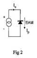
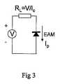
図2は、固定バイアス電圧ではなく、定電流源でバイアスされるEAMを簡単に表す。そのような定電流源は電気技術上周知であり、詳細に説明する必要はない。EAMの光電流Ipは、図3に示されるテブナン等価回路の考察によって推論され得るように、あるいは少なくとも説明され得るように、必ず賦課バイアス電流Icと等しくならなければならない。光電流が賦課電流より大きくなれば、等価抵抗RLにわたる電圧降下が大きくなり、バイアス電圧が低下し、よって光電流が小さくなるであろう。光電流が賦課電流より小さくなれば、逆のことがおこるであろう。したがって、EAM吸収及びEAMの感度は、均衡がとられてIc=Ip=ηPaとなるように、自動的に調節されなければならない。ここでPaは吸収されるパワーである。入力光信号の変調度が一定であれば、EAMによって発生されるRF信号の振幅も一定になるであろう。これは、定電流源の動作範囲をこえなければ、広い範囲の周囲温度、入力光レベル、入力波長及び偏光状態に対して、成立し続ける。FIG. 2 simply represents EAM biased with a constant current source rather than a fixed bias voltage. Such constant current sources are well known in the electrical art and need not be described in detail. The EAM photocurrent Ip must always be equal to the imposed bias current Ic , as can be inferred, or at least explained, by consideration of the Thevenin equivalent circuit shown in FIG. If the photocurrent is greater than the imposed current, the voltage drop across the equivalent resistanceRL will increase and the bias voltage will decrease, thus reducing the photocurrent. If the photocurrent is less than the imposed current, the reverse will occur. Thus, the sensitivity of the EAM absorption and the EAM, equilibrium is taken so that Ic = Ip = ηPa, must be adjusted automatically. Where Pa is the power absorbed. If the modulation degree of the input optical signal is constant, the amplitude of the RF signal generated by the EAM will also be constant. This continues to hold for a wide range of ambient temperatures, input light levels, input wavelengths and polarization states, unless the operating range of the constant current source is exceeded.
EAM内で有効に吸収される光パワーPaはRgcPiに等しいことが認められるであろう。ここで、Rは与えられたバイアス電圧におけるEAMの活性領域の吸収係数、Piは入射光パワー、gcは光入射端において結合領域を通ってデバイスの活性部分に到達する入射光の比率である。アンペア/ワット単位の(損失を無視する)理想感度はηRとなるであろう。ここでηは波長依存パラメータであり、代表的な遠距離通信波長の1550nmにおける値は1.25に近い。したがって、デバイスの活性領域の光の透過率はT=1―R=1―Ic/(ηgcPi)となる。したがって、Piの調節によって、限られた範囲内で、T(またはR)を任意に選ぶことができる。図1が、既に説明したように、代表的なEAMについて感度の外部回路測定値対DCバイアス電圧を示すことに留意すれば、このことを明確にすることができる。図1からわかるように、バイアスが−5Vに近い場合には、電圧依存吸収係数がその最大値にあるため、極めて僅かな光しか透過しない。外部測定感度は0.9A/Wより僅かに低い最大値を有する。これは、式:
に対応する。Corresponding to
対応実験
実験結果は、出願人等が(いかなる理論にも束縛されるつもりはなく)電子及び正孔の特性輸送時間の差に起因する、バイアス電圧によるEAMの周波数応答変動によると考える、上記の簡単な理論の予測からの少しではあるが決して無視できない、ただし本発明の有用性を減じることはない、系統的逸脱を示す。例として、この効果を全く考慮していない初期の設計の、図1のグラフをつくるために用いられたEAMは、0.22mAの定電流源でバイアスされ、電気的出力及びバイアス電圧は8〜30℃の範囲にわたる温度の関数として測定された。結果が図4にグラフで示され、出力は約0.7dBの範囲で一定ではあるが、バイアス電圧にしたがってほぼ線形態様で変化することを示した。The results of thecorresponding experimental experiment are considered to be due to variations in the frequency response of the EAM due to the bias voltage caused by the applicants (not intending to be bound by any theory) due to differences in the characteristic transport time of electrons and holes. It represents a systematic deviation that is a little from the prediction of a simple theory, but can never be ignored, but does not diminish the usefulness of the present invention. As an example, the EAM used to produce the graph of FIG. 1 in an early design that did not take this effect into account was biased with a constant current source of 0.22 mA, and the electrical output and bias voltage was 8 to Measured as a function of temperature over a range of 30 ° C. The results are shown graphically in FIG. 4 and show that the output is constant in the range of about 0.7 dB, but varies in a substantially linear fashion according to the bias voltage.
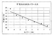
図5及び6は、ある範囲の入力光パワーレベルにわたる、同じ定電流バイアス条件の下での、このEAMの応答を示し、(EAM伝達特性の最も注目され、最も急峻な領域に対応する)測定範囲にわたり、入力光パワーが1dB低下する毎に電力出力がほぼ1dB増加したことを示す。図6はこの効果がいかにバイアス電圧に関して際立って線形であるかを示す。これらの変化は比較的小さく、本発明の有用性を減じることはない。必要であれば、制御アルゴリズムで対処することができる。EAMの適切な選択により、現在の定電流源で実用目的には十分であると考えられるが、(特定のEAM設計に対して)現在の動作条件についての最適バイアス電流を決定するためにルックアップテーブルまたはその他のコンピュータ演算の利用が必要であることがわかったとしても、最適バイアス電圧を直接に定めるために設計されるものよりかなり簡単なルックアップテーブルになるであろう。FIGS. 5 and 6 show the response of this EAM under the same constant current bias conditions over a range of input optical power levels, measuring (corresponding to the most noticeable and steepest region of EAM transfer characteristics). Over the range, the power outputincreased by approximately 1 dB for every 1 dB decrease in input optical power. FIG. 6 shows how this effect is remarkably linear with respect to the bias voltage. These changes are relatively small and do not diminish the usefulness of the present invention. If necessary, it can be handled by a control algorithm. With proper selection of EAM, current constant current sources may be sufficient for practical purposes, but look up to determine the optimal bias current for current operating conditions (for a particular EAM design) Even if it turns out that the use of a table or other computer operation is necessary, it will be a much simpler look-up table than that designed to directly determine the optimum bias voltage.
このタイプのシステムのEAMの変調効率に影響する別の要因は、EAMが電圧駆動システムであるため、一般に負荷インピーダンスが高くなるほど効率が高くなり、無線通信範囲が広くなるであろうという意味において、受動(無バイアス印加)モードにおいて、発現する電圧は応答曲線の実質的に線形領域から外れるほど大きくてはならないという重要な条件付で、負荷インピーダンスである。 Another factor that affects the modulation efficiency of EAM in this type of system is that, since EAM is a voltage driven system, in general, the higher the load impedance, the higher the efficiency and the wider the radio communication range. In the passive (unbiased) mode, the developed voltage is a load impedance, with the important condition that it must not be so great that it deviates from the substantially linear region of the response curve.
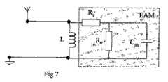
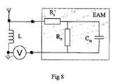
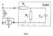
EAM自体がかなり大きな静電容量を有し、したがって、無線周波数において、比較的低インピーダンスのシャントを提供するから、EAMに高抵抗を接続しただけで有効に高められた効率を達成することには必ずしもならない。本発明の別の態様は、変換器の動作範囲内の周波数において共振する並列同調回路をEAMの内部容量と形成することによって、このシャント効果を低減し、可能であれば実質的に排除することである。図7〜9はそれぞれ、これを行う手段の1つを示す。 Since EAM itself has a fairly large capacitance and therefore provides a relatively low impedance shunt at radio frequencies, to achieve an effectively increased efficiency simply by connecting a high resistance to EAM. Not necessarily. Another aspect of the present invention reduces this shunt effect and, if possible, substantially eliminates it by forming a parallel tuning circuit with the EAM internal capacitance that resonates at frequencies within the operating range of the converter. It is. FIGS. 7-9 each show one means of doing this.
図7は、いかなる増幅またはバイアス印加もなく、したがって電力を全く必要としない、「受動ピコセル」設備を表す。EAM(ハッチング付矩形)は、直列抵抗RS,静電容量Cm及び、Pi・∂R(V)/∂Vの逆数を意味する、動的光抵抗R0からなる電気的等価回路で表される。ここで、Piは入射光パワー、∂R(V)/∂VはEAM感度対バイアス電圧曲線(この曲線は後にさらに論じられる)の勾配である。本発明にしたがえば、外部負荷は、一般には1〜100GHzの範囲、例えば無線ローカルエリアネットワークでの使用に対しては2.4または5.2GHz、あるいは「G3」セル式携帯電話ネットワークに対しては2GHzの、変換器の動作周波数範囲(の中央またはその近傍であることが好ましい)において共振する並列同調回路をCmと形成するように選ばれるインダクタンスLである。他の唯一の基本的なコンポーネントはアンテナであるが、フィーダー及びアンテナ整合ユニットがともなうことが多いであろう。代表的なデバイス及び設備パラメータ(原理的に、結合損失、感度及び推定光レベル)に対して、ゼロバイアスにおける最大光電流は1mAのオーダーであると思われ、したがって50Ωの負荷インピーダンスにおいては、約0.6Vの開路値と比較して、約0.05Vのピーク順電圧が生じる。0.05Vにおいて感度は実質的に線形のはずであり、開路においては実質的に対数感度が予想される。非線形性が許容できなくなる負荷インピーダンス値はデバイス毎に変わり、いずれにせよある程度主観的であって、当業者であれば、いかなる特定のEAMに対しても最善のインピーダンス値を決定し、達成することができるであろう。FIG. 7 represents a “passive picocell” facility that does not require any amplification or biasing and therefore requires no power. EAM (hatched rectangle) is an electrical equivalent circuit composed of a series resistance RS , a capacitance Cm and a dynamic photoresistance R0 , which means the reciprocal of Pi · ∂R (V) / ∂V. expressed. Where Pi is the incident light power and ∂R (V) / ∂V is the slope of the EAM sensitivity vs. bias voltage curve (this curve will be further discussed later). In accordance with the present invention, the external load is typically in the range of 1-100 GHz, for example 2.4 or 5.2 GHz for use in a wireless local area network, or for a "G3" cellular cellular network. Inductance L chosen to form a parallel tuning circuit with Cm that resonates in the operating frequency range (preferably at or near the center) of the transducer, typically 2 GHz. The only other basic component is an antenna, but it will often be accompanied by a feeder and an antenna matching unit. For typical device and equipment parameters (in principle, coupling loss, sensitivity and estimated light level), the maximum photocurrent at zero bias appears to be on the order of 1 mA, so at 50 Ω load impedance it is about Compared to the open circuit value of 0.6V, a peak forward voltage of about 0.05V occurs. Sensitivity should be substantially linear at 0.05V, and a logarithmic sensitivity is expected in the open circuit. The load impedance value at which the non-linearity becomes unacceptable varies from device to device and is somewhat subjective anyway, and those skilled in the art should determine and achieve the best impedance value for any particular EAM. Will be able to.
EAMにバイアスが適当に印加されている場合、そのような制限は生じない。図8は従来の設定電圧バイアス印加構成を示し、図9は本発明にしたがう定電流バイアス印加構成を示す。いずれの場合も、同調回路のQ因子は所要の信号変調帯域幅に調整することができ、固有の直列抵抗RS及び動的光抵抗R0によって設定される制限が課せられる。Such a limitation does not occur if the EAM is properly biased. FIG. 8 shows a conventional setting voltage bias application configuration, and FIG. 9 shows a constant current bias application configuration according to the present invention. In either case, the Q factor of the tuning circuit can be adjusted to the required signal modulation bandwidth, subject to restrictions set by the inherent series resistance RS and the dynamic optical resistance R0 .
図10は、本発明のこの態様に関するシミュレーションに用いられた、特定のEAMについての特性曲線を示す。図10は全般的には図1に対応するが、プロットされる方向が逆転し、縦軸の表示が入れ代わっていることに注意されたい。ゼロバイアスにおいて、感度対バイアス電圧曲線の勾配は約+0.25であり、Pi=2.5mWに対してR0は約1.33kΩになろう。R0はPiに反比例し、よって同調回路のQ因子は入射光パワーの増大にともなって低下するであろう。FIG. 10 shows the characteristic curve for a particular EAM used in the simulation for this aspect of the invention. FIG. 10 generally corresponds to FIG. 1, but note that the plotted direction is reversed and the vertical axis display is swapped. At zero bias, the slope of the sensitivity vs. bias voltage curve is about +0.25, and for Pi = 2.5 mW, R0 will be about 1.33 kΩ. R0 is inversely proportional to Pi, thus Q factor of the tuned circuit will drop with increasing incident light power.
図11はROF設備のリモートアンテナユニット1としての情況において本発明の変換器を例示する。リモートアンテナユニット1は、基地局2のレーザ送信器5からEAM6の光入力側に、またEAM6の光出力側から基地局2の光検出器7に、それぞれ光信号を伝送する2本の光ファイバ3及び4によって基地局2に接続される。定電流源8及び誘導性負荷インピーダンス9が先に説明したようにEAM6に接続され、EAM6の電気信号ポートが、負荷インピーダンス9と一体化することができるアンテナ整合ユニット10及びフィーダー11を介して、ダイポールと想定される双方向アンテナ12に接続され、この場合接地接続は必要に応じる。電力を高効率で伝送することよりも比較的高い電圧レベルを達成することが重要であり得るから、アンテナ整合ユニットは、最適電力伝送のためにEAMとアンテナのインピーダンスを等化するという狭い意味では、EAMとアンテナのインピーダンスを整合させ得ないことに注意されたい。基地局2において、上流信号の一部は相互変調歪モニタ13への入力として用いられ、相互変調歪モニタ13は続いて、十分な上流無線周波数信号電力及び低相互変調歪を保証し、全体的には電流動作条件にしたがって設備を最適化するように、レーザ5からの出力の振幅を調節してEAMバイアス点を設定する、振幅制御器14への入力(必ずしも唯一の入力ではない)を供給する。 FIG. 11 illustrates the converter of the present invention in the context of the
市販のマイクロ波シミュレーションソフトウエア「DragonWave 7.0(商標)」を用いるシミュレーションは、少なくとも5のQ因子及び約250Ωの実効EAM負荷インピーダンスを実用可能なコンポーネント値で達成できることを示し、これは実験で確認された。適切な特定のコンポーネント値は特定のEAMの関数であるが、当業者が決定できる範囲にある。EAMの静電容量Cmの値の低減は有益であり、光路長及び変調度を維持すると同時にデバイスの物理長を1/2にすることが可能になるから、これは反射型EAMの使用における有利性を示すことに注意されたい。Simulations using the commercially available microwave simulation software “DragonWave 7.0 ™” show that a Q factor of at least 5 and an effective EAM load impedance of about 250Ω can be achieved with practical component values, which has been confirmed experimentally. It was. A suitable specific component value is a function of a specific EAM, but is within a range that can be determined by one skilled in the art. Reducing the value of the EAM capacitance Cm is beneficial and allows the physical length of the device to be halved while maintaining the optical path length and degree of modulation, which is the reason for using reflective EAM. Note that it shows an advantage.
本発明の精神及び範囲を逸脱することなく本発明に様々な改変及び変形がなされ得ることが当業者には明らかであろう。したがって、添付される特許請求項及びそれらの等価物の範囲内に本発明の改変及び変形が入れば、本発明はそのような改変及び変形を包含するとされる。 It will be apparent to those skilled in the art that various modifications and variations can be made to the present invention without departing from the spirit and scope of the invention. Therefore, it is intended that the present invention cover such modifications and variations as come within the scope of the appended claims and their equivalents.
本明細書における本発明に関する背景技術のいかなる議論も本発明の状況を説明するために含められる。いずれかの文書または情報が「既知」とされる場合、本出願の日付の前にどこかで公衆の少なくとも一員に知られていたことだけが認められる。そうではなく参考文献の内容が明確に示していなければ、そのような知識が印刷出版物に述べられていたか、あるいは、公衆または米国または(PCTの同盟国であるか否かにかかわらず)いかなる特定の国においても本発明が関係する技術の当業者に利用可能であったか、あるいは、本発明がなされる以前またはいかなる特許請求日付以前に知られていたかまたは開示されていたとは認められない。さらに、いずれかの文書または情報が、全世界ベースでも、いずれの国においても、技術の共通一般知識の一部を形成するとは認められず、どれか1つでもそうするとは考えられない。 Any discussion of background art related to the invention herein is included to describe the context of the invention. If any document or information is deemed "known", it is only accepted that it was known to at least one member of the public somewhere before the date of this application. Otherwise, if the content of the bibliography is not clearly indicated, such knowledge was stated in the printed publication, or any identification of the public or the United States or (whether or not a PCT ally) It is not recognized in any country that the present invention was available to those skilled in the art to which the present invention pertained or was known or disclosed before the invention was made or before any claim date. In addition, no document or information is recognized to form part of the common general knowledge of technology, either on a global basis or in any country, and no one is considered to do so.
1 リモートアンテナユニット
2 基地局
3,4 光ファイバ
5 レーザ送信器
6 EAM
7 光検出器
8 定電流源
9 誘導性負荷インピーダンス
10 アンテナ整合ユニット
11 フィーダー
12 双方向アンテナ
13 相互変調歪モニタ
14 振幅制御器DESCRIPTION OF
7
Claims (10)
Translated fromJapanese請求項1に記載の変換器を備えるリモートアンテナユニット、及び
下流光信号源、上流光信号のための検出器及び前記変換器の光入力振幅の調節によって前記変換器の動作を最適化するための振幅制御器を備える基地局、
を有することを特徴とする光ファイバ無線設備。In optical fiber radio equipment,
A remote antenna unit comprising the converter of claim 1, and a downstream optical signal source, a detector for the upstream optical signal, and optimizing the operation of the converter by adjusting the optical input amplitude of the converter A base station with an amplitude controller,
An optical fiber radio equipment comprising:
Applications Claiming Priority (2)
| Application Number | Priority Date | Filing Date | Title |
|---|---|---|---|
| US10/966,509US20060083520A1 (en) | 2004-10-15 | 2004-10-15 | Communication by radio waves and optical waveguides |
| PCT/US2005/036784WO2006044519A2 (en) | 2004-10-15 | 2005-10-13 | Communication by radio waves and optical waveguides |
Publications (1)
| Publication Number | Publication Date |
|---|---|
| JP2008517534Atrue JP2008517534A (en) | 2008-05-22 |
Family
ID=36180871
Family Applications (1)
| Application Number | Title | Priority Date | Filing Date |
|---|---|---|---|
| JP2007536872AAbandonedJP2008517534A (en) | 2004-10-15 | 2005-10-13 | Communication using radio waves and optical waveguides |
Country Status (6)
| Country | Link |
|---|---|
| US (2) | US20060083520A1 (en) |
| EP (1) | EP1800421A4 (en) |
| JP (1) | JP2008517534A (en) |
| CN (1) | CN101040466A (en) |
| TW (1) | TW200637198A (en) |
| WO (1) | WO2006044519A2 (en) |
Families Citing this family (76)
| Publication number | Priority date | Publication date | Assignee | Title |
|---|---|---|---|---|
| EP1971036A1 (en)* | 2007-03-14 | 2008-09-17 | Dtu | A method and a device for detection of a first signal superimposed on a second signal |
| WO2009114738A2 (en)* | 2008-03-12 | 2009-09-17 | Hypres, Inc. | Digital radio-frequency tranceiver system and method |
| CN101346006B (en)* | 2008-08-19 | 2011-01-19 | 武汉长光科技有限公司 | Radio frequency passive optical network with broadband wireless and optical transmission amalgamation access |
| CN102369678B (en) | 2009-02-03 | 2015-08-19 | 康宁光缆系统有限责任公司 | Optical fiber based distributed antenna systems, assemblies and related methods for calibrating optical fiber based distributed antenna systems, assemblies |
| CN102396171B (en) | 2009-02-03 | 2015-09-30 | 康宁光缆系统有限责任公司 | Based on the distributing antenna system of optical fiber, assembly and the correlation technique for monitoring and configure distributing antenna system based on optical fiber, assembly |
| US9673904B2 (en) | 2009-02-03 | 2017-06-06 | Corning Optical Communications LLC | Optical fiber-based distributed antenna systems, components, and related methods for calibration thereof |
| FR2951322B1 (en) | 2009-10-09 | 2011-12-09 | Dcns | WIRELESS ANTENNA SYSTEM FOR RECEIVING RADIO SIGNALS, IN PARTICULAR FOR A SHIP |
| US8280259B2 (en) | 2009-11-13 | 2012-10-02 | Corning Cable Systems Llc | Radio-over-fiber (RoF) system for protocol-independent wired and/or wireless communication |
| EP2330757A1 (en)* | 2009-12-07 | 2011-06-08 | BRITISH TELECOMMUNICATIONS public limited company | Wireless connector |
| US8275265B2 (en) | 2010-02-15 | 2012-09-25 | Corning Cable Systems Llc | Dynamic cell bonding (DCB) for radio-over-fiber (RoF)-based networks and communication systems and related methods |
| US9252874B2 (en) | 2010-10-13 | 2016-02-02 | Ccs Technology, Inc | Power management for remote antenna units in distributed antenna systems |
| WO2012148940A1 (en) | 2011-04-29 | 2012-11-01 | Corning Cable Systems Llc | Systems, methods, and devices for increasing radio frequency (rf) power in distributed antenna systems |
| WO2012148938A1 (en) | 2011-04-29 | 2012-11-01 | Corning Cable Systems Llc | Determining propagation delay of communications in distributed antenna systems, and related components, systems and methods |
| EP2523369A1 (en) | 2011-05-12 | 2012-11-14 | Mikko Väänänen | Broadband base station comprising means for free space optical communications |
| CA2836133A1 (en) | 2011-05-17 | 2012-11-22 | 3M Innovative Properties Company | Converged in-building network |
| US8606110B2 (en)* | 2012-01-08 | 2013-12-10 | Optiway Ltd. | Optical distributed antenna system |
| WO2013162988A1 (en) | 2012-04-25 | 2013-10-31 | Corning Cable Systems Llc | Distributed antenna system architectures |
| WO2014024192A1 (en) | 2012-08-07 | 2014-02-13 | Corning Mobile Access Ltd. | Distribution of time-division multiplexed (tdm) management services in a distributed antenna system, and related components, systems, and methods |
| US9455784B2 (en) | 2012-10-31 | 2016-09-27 | Corning Optical Communications Wireless Ltd | Deployable wireless infrastructures and methods of deploying wireless infrastructures |
| US9647758B2 (en) | 2012-11-30 | 2017-05-09 | Corning Optical Communications Wireless Ltd | Cabling connectivity monitoring and verification |
| CN105452951B (en) | 2013-06-12 | 2018-10-19 | 康宁光电通信无线公司 | Voltage type optical directional coupler |
| WO2014199380A1 (en) | 2013-06-12 | 2014-12-18 | Corning Optical Communications Wireless, Ltd. | Time-division duplexing (tdd) in distributed communications systems, including distributed antenna systems (dass) |
| US9247543B2 (en) | 2013-07-23 | 2016-01-26 | Corning Optical Communications Wireless Ltd | Monitoring non-supported wireless spectrum within coverage areas of distributed antenna systems (DASs) |
| US9661781B2 (en) | 2013-07-31 | 2017-05-23 | Corning Optical Communications Wireless Ltd | Remote units for distributed communication systems and related installation methods and apparatuses |
| US9385810B2 (en) | 2013-09-30 | 2016-07-05 | Corning Optical Communications Wireless Ltd | Connection mapping in distributed communication systems |
| US9178635B2 (en) | 2014-01-03 | 2015-11-03 | Corning Optical Communications Wireless Ltd | Separation of communication signal sub-bands in distributed antenna systems (DASs) to reduce interference |
| US9775123B2 (en) | 2014-03-28 | 2017-09-26 | Corning Optical Communications Wireless Ltd. | Individualized gain control of uplink paths in remote units in a distributed antenna system (DAS) based on individual remote unit contribution to combined uplink power |
| US9357551B2 (en) | 2014-05-30 | 2016-05-31 | Corning Optical Communications Wireless Ltd | Systems and methods for simultaneous sampling of serial digital data streams from multiple analog-to-digital converters (ADCS), including in distributed antenna systems |
| US9730228B2 (en) | 2014-08-29 | 2017-08-08 | Corning Optical Communications Wireless Ltd | Individualized gain control of remote uplink band paths in a remote unit in a distributed antenna system (DAS), based on combined uplink power level in the remote unit |
| US9602210B2 (en) | 2014-09-24 | 2017-03-21 | Corning Optical Communications Wireless Ltd | Flexible head-end chassis supporting automatic identification and interconnection of radio interface modules and optical interface modules in an optical fiber-based distributed antenna system (DAS) |
| US9420542B2 (en) | 2014-09-25 | 2016-08-16 | Corning Optical Communications Wireless Ltd | System-wide uplink band gain control in a distributed antenna system (DAS), based on per band gain control of remote uplink paths in remote units |
| US9973299B2 (en) | 2014-10-14 | 2018-05-15 | At&T Intellectual Property I, L.P. | Method and apparatus for adjusting a mode of communication in a communication network |
| US9312919B1 (en) | 2014-10-21 | 2016-04-12 | At&T Intellectual Property I, Lp | Transmission device with impairment compensation and methods for use therewith |
| US10243784B2 (en) | 2014-11-20 | 2019-03-26 | At&T Intellectual Property I, L.P. | System for generating topology information and methods thereof |
| US9954287B2 (en) | 2014-11-20 | 2018-04-24 | At&T Intellectual Property I, L.P. | Apparatus for converting wireless signals and electromagnetic waves and methods thereof |
| US10009067B2 (en) | 2014-12-04 | 2018-06-26 | At&T Intellectual Property I, L.P. | Method and apparatus for configuring a communication interface |
| US9997819B2 (en) | 2015-06-09 | 2018-06-12 | At&T Intellectual Property I, L.P. | Transmission medium and method for facilitating propagation of electromagnetic waves via a core |
| US9461706B1 (en) | 2015-07-31 | 2016-10-04 | At&T Intellectual Property I, Lp | Method and apparatus for exchanging communication signals |
| US20160249365A1 (en) | 2015-02-19 | 2016-08-25 | Corning Optical Communications Wireless Ltd. | Offsetting unwanted downlink interference signals in an uplink path in a distributed antenna system (das) |
| US9876570B2 (en) | 2015-02-20 | 2018-01-23 | At&T Intellectual Property I, Lp | Guided-wave transmission device with non-fundamental mode propagation and methods for use therewith |
| US9681313B2 (en) | 2015-04-15 | 2017-06-13 | Corning Optical Communications Wireless Ltd | Optimizing remote antenna unit performance using an alternative data channel |
| US10224981B2 (en) | 2015-04-24 | 2019-03-05 | At&T Intellectual Property I, Lp | Passive electrical coupling device and methods for use therewith |
| US9705561B2 (en) | 2015-04-24 | 2017-07-11 | At&T Intellectual Property I, L.P. | Directional coupling device and methods for use therewith |
| US9490869B1 (en) | 2015-05-14 | 2016-11-08 | At&T Intellectual Property I, L.P. | Transmission medium having multiple cores and methods for use therewith |
| US9871282B2 (en) | 2015-05-14 | 2018-01-16 | At&T Intellectual Property I, L.P. | At least one transmission medium having a dielectric surface that is covered at least in part by a second dielectric |
| US10650940B2 (en) | 2015-05-15 | 2020-05-12 | At&T Intellectual Property I, L.P. | Transmission medium having a conductive material and methods for use therewith |
| US9866309B2 (en) | 2015-06-03 | 2018-01-09 | At&T Intellectual Property I, Lp | Host node device and methods for use therewith |
| US9912381B2 (en) | 2015-06-03 | 2018-03-06 | At&T Intellectual Property I, Lp | Network termination and methods for use therewith |
| US9913139B2 (en) | 2015-06-09 | 2018-03-06 | At&T Intellectual Property I, L.P. | Signal fingerprinting for authentication of communicating devices |
| US9820146B2 (en) | 2015-06-12 | 2017-11-14 | At&T Intellectual Property I, L.P. | Method and apparatus for authentication and identity management of communicating devices |
| US9865911B2 (en) | 2015-06-25 | 2018-01-09 | At&T Intellectual Property I, L.P. | Waveguide system for slot radiating first electromagnetic waves that are combined into a non-fundamental wave mode second electromagnetic wave on a transmission medium |
| US9640850B2 (en) | 2015-06-25 | 2017-05-02 | At&T Intellectual Property I, L.P. | Methods and apparatus for inducing a non-fundamental wave mode on a transmission medium |
| US9853342B2 (en) | 2015-07-14 | 2017-12-26 | At&T Intellectual Property I, L.P. | Dielectric transmission medium connector and methods for use therewith |
| US9847566B2 (en) | 2015-07-14 | 2017-12-19 | At&T Intellectual Property I, L.P. | Method and apparatus for adjusting a field of a signal to mitigate interference |
| US10044409B2 (en) | 2015-07-14 | 2018-08-07 | At&T Intellectual Property I, L.P. | Transmission medium and methods for use therewith |
| US10090606B2 (en) | 2015-07-15 | 2018-10-02 | At&T Intellectual Property I, L.P. | Antenna system with dielectric array and methods for use therewith |
| US9948349B2 (en) | 2015-07-17 | 2018-04-17 | Corning Optical Communications Wireless Ltd | IOT automation and data collection system |
| US9871283B2 (en) | 2015-07-23 | 2018-01-16 | At&T Intellectual Property I, Lp | Transmission medium having a dielectric core comprised of plural members connected by a ball and socket configuration |
| US9749053B2 (en) | 2015-07-23 | 2017-08-29 | At&T Intellectual Property I, L.P. | Node device, repeater and methods for use therewith |
| US9948333B2 (en) | 2015-07-23 | 2018-04-17 | At&T Intellectual Property I, L.P. | Method and apparatus for wireless communications to mitigate interference |
| US9912027B2 (en) | 2015-07-23 | 2018-03-06 | At&T Intellectual Property I, L.P. | Method and apparatus for exchanging communication signals |
| US9967173B2 (en) | 2015-07-31 | 2018-05-08 | At&T Intellectual Property I, L.P. | Method and apparatus for authentication and identity management of communicating devices |
| US9904535B2 (en) | 2015-09-14 | 2018-02-27 | At&T Intellectual Property I, L.P. | Method and apparatus for distributing software |
| US10560214B2 (en) | 2015-09-28 | 2020-02-11 | Corning Optical Communications LLC | Downlink and uplink communication path switching in a time-division duplex (TDD) distributed antenna system (DAS) |
| US9876264B2 (en) | 2015-10-02 | 2018-01-23 | At&T Intellectual Property I, Lp | Communication system, guided wave switch and methods for use therewith |
| US10236924B2 (en) | 2016-03-31 | 2019-03-19 | Corning Optical Communications Wireless Ltd | Reducing out-of-channel noise in a wireless distribution system (WDS) |
| US9860075B1 (en) | 2016-08-26 | 2018-01-02 | At&T Intellectual Property I, L.P. | Method and communication node for broadband distribution |
| US10811767B2 (en) | 2016-10-21 | 2020-10-20 | At&T Intellectual Property I, L.P. | System and dielectric antenna with convex dielectric radome |
| US10312567B2 (en) | 2016-10-26 | 2019-06-04 | At&T Intellectual Property I, L.P. | Launcher with planar strip antenna and methods for use therewith |
| US10225025B2 (en) | 2016-11-03 | 2019-03-05 | At&T Intellectual Property I, L.P. | Method and apparatus for detecting a fault in a communication system |
| US10178445B2 (en) | 2016-11-23 | 2019-01-08 | At&T Intellectual Property I, L.P. | Methods, devices, and systems for load balancing between a plurality of waveguides |
| US10637149B2 (en) | 2016-12-06 | 2020-04-28 | At&T Intellectual Property I, L.P. | Injection molded dielectric antenna and methods for use therewith |
| US10389037B2 (en) | 2016-12-08 | 2019-08-20 | At&T Intellectual Property I, L.P. | Apparatus and methods for selecting sections of an antenna array and use therewith |
| US9998870B1 (en) | 2016-12-08 | 2018-06-12 | At&T Intellectual Property I, L.P. | Method and apparatus for proximity sensing |
| US9838896B1 (en) | 2016-12-09 | 2017-12-05 | At&T Intellectual Property I, L.P. | Method and apparatus for assessing network coverage |
| CN112804007B (en)* | 2021-04-13 | 2021-08-31 | 网络通信与安全紫金山实验室 | Dual-signal modulation and demodulation method and device for radio-over-fiber communication system |
Family Cites Families (4)
| Publication number | Priority date | Publication date | Assignee | Title |
|---|---|---|---|---|
| CA2127060A1 (en)* | 1993-06-30 | 1994-12-31 | Hiromitsu Kawamura | Modulator integrated distributed feed-back laser diode module and device using the same |
| JP2827977B2 (en)* | 1995-07-14 | 1998-11-25 | 日本電気株式会社 | Modulation circuit of semiconductor optical modulator |
| KR100555996B1 (en)* | 1996-07-19 | 2006-07-06 | 넥스트지 네트웍스 인코퍼레이티드 | Telecommunication system that receives and modulates optical signals simultaneously |
| US6788447B2 (en)* | 2002-08-07 | 2004-09-07 | Triquint Technology Holding Co. | Off-chip matching circuit for electroabsorption optical modulator |
- 2004
- 2004-10-15USUS10/966,509patent/US20060083520A1/ennot_activeAbandoned
- 2005
- 2005-10-13EPEP05820929Apatent/EP1800421A4/ennot_activeWithdrawn
- 2005-10-13JPJP2007536872Apatent/JP2008517534A/ennot_activeAbandoned
- 2005-10-13WOPCT/US2005/036784patent/WO2006044519A2/enactiveApplication Filing
- 2005-10-13CNCNA2005800353553Apatent/CN101040466A/enactivePending
- 2005-10-14TWTW094136245Apatent/TW200637198A/enunknown
- 2007
- 2007-11-15USUS11/985,488patent/US20080101798A1/ennot_activeAbandoned
Also Published As
| Publication number | Publication date |
|---|---|
| CN101040466A (en) | 2007-09-19 |
| US20080101798A1 (en) | 2008-05-01 |
| EP1800421A2 (en) | 2007-06-27 |
| WO2006044519A2 (en) | 2006-04-27 |
| TW200637198A (en) | 2006-10-16 |
| WO2006044519A3 (en) | 2007-02-01 |
| US20060083520A1 (en) | 2006-04-20 |
| EP1800421A4 (en) | 2008-01-23 |
Similar Documents
| Publication | Publication Date | Title |
|---|---|---|
| JP2008517534A (en) | Communication using radio waves and optical waveguides | |
| JP3411947B2 (en) | Radio-to-optical conversion modulator and communication system using the same | |
| AU631075B2 (en) | Reconfigurable rf matching circuit | |
| JP2004032412A (en) | Optical transmission system | |
| JPH07264143A (en) | Optically and electrically controlled RF matching circuit | |
| TW201336251A (en) | Communications device with discriminator for generating intermediate frequency signal and related methods | |
| JPH07143182A (en) | Optical transmission device | |
| US5907422A (en) | Universal optical signal receiver | |
| TW201519588A (en) | Optical signal conversion system and method using period-one nonlinear dynamics of semiconductor lasers | |
| Nagatsuma et al. | SiC-substrate uni-traveling-carrier photodiode modules for 300-GHz-band wireless communications | |
| Chen et al. | High-Speed $ W $-Band Integrated Photonic Transmitter for Radio-Over-Fiber Applications | |
| Urzçdowska et al. | Radio-over-fiber link for WLAN and LTE systems | |
| US10826729B1 (en) | Communication system with adjustable equalization levels and related methods | |
| Tessema et al. | A photonics-assisted beamformer for K-band RF antenna arrays | |
| Bogaert et al. | Narrowband photoreceiver for analog radio-over-fiber in the 24.25-29.5 GHz band | |
| JP4568159B2 (en) | Bidirectional WDM optical analog transmission system | |
| JP2014053879A (en) | Tv optical transmission system configuration | |
| KR101438355B1 (en) | Linear analog optical transmitter with IM3 cancellation function | |
| Kukutsu et al. | 10-Gbit/s wireless transmission systems using 120-GHz-band photodiode and MMIC technologies | |
| CN114024613B (en) | Polarization multiplexing high-linearity full-duplex optical carrier radio frequency link device and method | |
| Salleh et al. | Design the High Gain and Low Power Amplifier for Radio over Fiber Technology at 2.4 GHz | |
| Niiho et al. | Radio-on-fiber link using direct modulation in 5-GHz band | |
| Radi et al. | Towards Integrated RF Photodetector-Antenna Emitters in Silicon Photonics | |
| JP5092080B2 (en) | Light modulator | |
| JPWO2022058790A5 (en) |
Legal Events
| Date | Code | Title | Description |
|---|---|---|---|
| A621 | Written request for application examination | Free format text:JAPANESE INTERMEDIATE CODE: A621 Effective date:20081007 | |
| A762 | Written abandonment of application | Free format text:JAPANESE INTERMEDIATE CODE: A762 Effective date:20100203 |