JP2008516525A - Radio frequency identification tag and manufacturing method thereof - Google Patents
Radio frequency identification tag and manufacturing method thereofDownload PDFInfo
- Publication number
- JP2008516525A JP2008516525AJP2007535679AJP2007535679AJP2008516525AJP 2008516525 AJP2008516525 AJP 2008516525AJP 2007535679 AJP2007535679 AJP 2007535679AJP 2007535679 AJP2007535679 AJP 2007535679AJP 2008516525 AJP2008516525 AJP 2008516525A
- Authority
- JP
- Japan
- Prior art keywords
- substrate
- rfid tag
- antenna
- positioning structure
- die
- Prior art date
- Legal status (The legal status is an assumption and is not a legal conclusion. Google has not performed a legal analysis and makes no representation as to the accuracy of the status listed.)
- Pending
Links
Images


Classifications
- G—PHYSICS
- G06—COMPUTING OR CALCULATING; COUNTING
- G06K—GRAPHICAL DATA READING; PRESENTATION OF DATA; RECORD CARRIERS; HANDLING RECORD CARRIERS
- G06K19/00—Record carriers for use with machines and with at least a part designed to carry digital markings
- G06K19/06—Record carriers for use with machines and with at least a part designed to carry digital markings characterised by the kind of the digital marking, e.g. shape, nature, code
- G06K19/067—Record carriers with conductive marks, printed circuits or semiconductor circuit elements, e.g. credit or identity cards also with resonating or responding marks without active components
- G06K19/07—Record carriers with conductive marks, printed circuits or semiconductor circuit elements, e.g. credit or identity cards also with resonating or responding marks without active components with integrated circuit chips
- G06K19/077—Constructional details, e.g. mounting of circuits in the carrier
- G06K19/07749—Constructional details, e.g. mounting of circuits in the carrier the record carrier being capable of non-contact communication, e.g. constructional details of the antenna of a non-contact smart card
- G06K19/0775—Constructional details, e.g. mounting of circuits in the carrier the record carrier being capable of non-contact communication, e.g. constructional details of the antenna of a non-contact smart card arrangements for connecting the integrated circuit to the antenna
- G—PHYSICS
- G06—COMPUTING OR CALCULATING; COUNTING
- G06K—GRAPHICAL DATA READING; PRESENTATION OF DATA; RECORD CARRIERS; HANDLING RECORD CARRIERS
- G06K19/00—Record carriers for use with machines and with at least a part designed to carry digital markings
- G06K19/06—Record carriers for use with machines and with at least a part designed to carry digital markings characterised by the kind of the digital marking, e.g. shape, nature, code
- G06K19/067—Record carriers with conductive marks, printed circuits or semiconductor circuit elements, e.g. credit or identity cards also with resonating or responding marks without active components
- G06K19/07—Record carriers with conductive marks, printed circuits or semiconductor circuit elements, e.g. credit or identity cards also with resonating or responding marks without active components with integrated circuit chips
- G06K19/077—Constructional details, e.g. mounting of circuits in the carrier
- G06K19/07749—Constructional details, e.g. mounting of circuits in the carrier the record carrier being capable of non-contact communication, e.g. constructional details of the antenna of a non-contact smart card
Landscapes
- Engineering & Computer Science (AREA)
- Microelectronics & Electronic Packaging (AREA)
- Computer Hardware Design (AREA)
- Physics & Mathematics (AREA)
- General Physics & Mathematics (AREA)
- Theoretical Computer Science (AREA)
- Details Of Aerials (AREA)
- Near-Field Transmission Systems (AREA)
Abstract
Translated fromJapaneseDescription
Translated fromJapanese本発明は、一般に無線通信の分野に関し、特に商品の移動の追跡並びにその他の適切な用途のための無線周波送信の使用に関する。 The present invention relates generally to the field of wireless communications, and more particularly to the use of radio frequency transmission for tracking the movement of goods and other suitable applications.
消費者は、商業経路を通過する商品の移動を認識し、表にし、そして索引化することに慣れている。日常的な例として、スーパーマーケットにおいて見られるような光学式スキャナーと組み合わされるバーコードがある。最近では、ある種の製品及びその容器に無線周波識別(RFID)トランスポーダーにより「タグ」が付けられている。これは、無線周波リーダー及び精巧なコンピューターシステムと組み合わせて、ある距離から在庫を追跡するための商業的な組織を可能とする。RFIDシステムはタグ、リーダー、及び関連データをコンパイルするためにリーダーに接続されたコンピューター回路網を備える。 Consumers are accustomed to recognizing, tabulating, and indexing the movement of goods through commercial channels. A routine example is a barcode combined with an optical scanner such as found in a supermarket. Recently, certain products and their containers have been “tagged” by radio frequency identification (RFID) transporters. This, in combination with a radio frequency reader and sophisticated computer system, allows commercial organizations to track inventory from a distance. The RFID system comprises a tag, a reader, and computer circuitry connected to the reader for compiling related data.
RFIDタグは、一般に基板材料より構成され、これに、無線信号の送受信用のアンテナが置かれる。アンテナはシリコンのチップ又はダイに接続され、これはそのタグが取り付けられる対象物に関するデータでエンコードされる。ダイ自体は、読出し専用メモリ(ROM)、電気的プログラム可能読出し専用メモリ(EPROM)、及び電気的消去及びプログラム可能読出し専用メモリ(EEPROM)を含む諸種のものとすることができる。タグは、使用されるダイの形式に応じて、データを記憶し、リーダーにデータを送信し、更に新しいデータ入力に適合するように再プログラムすることができる。 An RFID tag is generally made of a substrate material, on which an antenna for transmitting and receiving radio signals is placed. The antenna is connected to a silicon chip or die, which is encoded with data about the object to which the tag is attached. The die itself can be of various types including read only memory (ROM), electrically programmable read only memory (EPROM), and electrical erase and programmable read only memory (EEPROM). Depending on the type of die used, the tag can store data, send data to the reader, and can be reprogrammed to fit new data input.
RFIDタグは能動型と受動型との2形式になる。能動型タグは、電池のような電源を備え、これが、RFIDアンテナから端末受信機に必要なデータを送信するに十分な電流を提供する。受動型タブは、一般に能動型タグより小型であり、独立した電源を備えていない。能動型タグは、照会しているリーダーからの放射のような到来放射からその電力を得る。能動型タグは、その優れた寸法、重さ、及び価格のため、一般に、例えば、書籍及び輸送箱を含んだ高度に移動性の小売物品及び容器との使用に対して優れていると考えられる。 RFID tags come in two types, active and passive. The active tag has a power source such as a battery, which provides sufficient current to transmit the necessary data from the RFID antenna to the terminal receiver. Passive tabs are generally smaller than active tags and do not have a separate power source. An active tag derives its power from incoming radiation, such as radiation from an interrogating reader. Active tags are generally considered superior for use with highly mobile retail items and containers, including, for example, books and shipping boxes, due to their superior size, weight, and price. .
能動型タグは、その利点にも拘わらず、その保守、操作、及び製造に伴う多くの問題点がある。特に、RFIDタグに対する商業及び可能な市場のシェアの大きさが与えられる場合、適切なタグの量産を妨げる製造工程における現在の幾つかの制限がある。 Active tags, despite their advantages, have a number of problems with their maintenance, operation, and manufacture. In particular, given the large commercial and possible market share for RFID tags, there are some current limitations in the manufacturing process that prevent mass production of appropriate tags.
RFIDタグの製造においては、シリコンダイを正確に置きアンテナに接続しなければならない。ダイの設置は、一般に、光学的アライメントを介してロボット技術により行われ、この際、ダイとアンテナとの間の接合を形成しなければならない。アンテナがダイに接合されると、接合剤が硬化される。硬化工程は、加熱、或いは接合剤中の光イニシエーター薬品と相互作用する紫外線(UV)放射を含み、これにより硬化過程を加速させることが普通である。典型的な工程においては、ダイをアンテナに接合するために、UV感受性の光イニシエーターを含んだエポキシが使用される。次いで、ほぼ3電子ボルト(eV)エネルギーの十分なホトンフルエンスでUV放射が接合部を照射し、その数秒後、エポキシが硬化し接合が形成される。 In manufacturing RFID tags, the silicon die must be accurately placed and connected to the antenna. Die placement is typically done by robot technology through optical alignment, in which a bond between the die and the antenna must be formed. When the antenna is bonded to the die, the bonding agent is cured. The curing process typically involves heating or ultraviolet (UV) radiation that interacts with the photoinitiator chemical in the binder, thereby accelerating the curing process. In a typical process, an epoxy containing a UV sensitive photoinitiator is used to bond the die to the antenna. UV radiation then irradiates the joint with sufficient photon fluence of approximately 3 electron volts (eV) energy, and after a few seconds, the epoxy cures and a bond is formed.
上述された工程はRFIDタグの量産を妨げる多くの困難な状況を与える。第1に、RFIDタグに対する経済上の要求が年産数十億個に達するので、8−10秒のUV硬化工
程が、製造業者の理論的に集め得る供給量を限定する。第2に、ダイがアンテナに接合されると、出荷前検査を通らなかった場合にダイを外す簡単な方法がない。その結果、RFIDタグの20−40%と見積もられる検査不合格のものは回収不能なロスであり、更に業者及び消費者に対するタグの供給を限定しかつ価格を高くする。The process described above presents many difficult situations that hinder mass production of RFID tags. First, as the economic demand for RFID tags reaches billions of annual output, the 8-10 second UV curing process limits the supply that can be theoretically collected by the manufacturer. Second, once the die is bonded to the antenna, there is no easy way to remove the die if it fails the pre-shipment inspection. As a result, 20-40% of RFID tags that fail inspection are unrecoverable losses, further limiting the supply of tags and increasing the price to merchants and consumers.
以上のようであるため、ある範囲の商業上の応用に有用な信頼性があり効果的かつ製造の容易なRFIDタグに対する要求がある。更に、信頼し得る試験パラメーターと高い生産量とを有するRFIDタグの経済的な新規な量産方法に対する要求がある。 As such, there is a need for a reliable, effective and easy to manufacture RFID tag that is useful for a range of commercial applications. In addition, there is a need for an economical new mass production method for RFID tags with reliable test parameters and high production volumes.
従って、本発明は、効率的で信頼できかつ高忠実度のRFIDタグ及びその製造方法を含む。本発明のRFIDタグは、上に無線周波信号を送受信するためのアンテナを印刷することができる基板を備える。RFIDタグは、基板上に配置されたダイ位置決め構造も備え、この構造は典型的にRFID用に使用される形式のシリコンダイを受け入れるために鋳造され固化される。シリコンダイは、少なくも1個の接合部によりアンテナと電気的に接続され、これによりRFIDタグは、送信、受信、及び、恐らくは通常のRFIDプロトコールによりシリコンダイに記憶された電子データの更新ができる。 Accordingly, the present invention includes an efficient, reliable and high fidelity RFID tag and method for manufacturing the same. The RFID tag of the present invention includes a substrate on which an antenna for transmitting and receiving radio frequency signals can be printed. The RFID tag also includes a die positioning structure disposed on the substrate, which is typically cast and solidified to accept a silicon die of the type used for RFID. The silicon die is electrically connected to the antenna by at least one junction, which allows the RFID tag to transmit, receive, and possibly update the electronic data stored on the silicon die according to the normal RFID protocol. .
変更実施例においては、本発明のRFIDタグは、ある範囲の応用及び管轄区域にわたり実施可能な周波数範囲にわたり作動可能である。例えば、アンテナは、これを400から1000メガヘルツの間で作動可能であるように選定することができる。より特別には、米国における改良された運用については、アンテナは915から920メガヘルツの間で作動可能なように選ぶことができる。周波数の低い用途に対しては、選択されたアンテナは100から150キロヘルツの間で作動可能であろうし、一方マイクロ波については、アンテナは2.4から2.5ギガヘルツの間で作動可能であろう。本発明のRFIDタグは、ある周波数範囲にわたる使用に容易に適合させることができ、従って消耗品から自動車構成要素及び動物の識別タグに至る用途範囲にわたり使用することができる。 In an alternative embodiment, the RFID tag of the present invention is operable over a range of frequencies that can be implemented over a range of applications and jurisdictions. For example, the antenna can be selected such that it can operate between 400 and 1000 megahertz. More specifically, for improved operation in the United States, the antenna can be chosen to operate between 915 and 920 megahertz. For low frequency applications, the selected antenna will be capable of operating between 100 and 150 kilohertz, while for microwaves the antenna may be operable between 2.4 and 2.5 gigahertz. Let's go. The RFID tag of the present invention can be easily adapted for use over a range of frequencies and thus can be used over a range of applications ranging from consumables to automotive components and animal identification tags.
本発明の新規なRFIDタグはRFID産業における改良された製造方法の結果である。この方法は、上にアンテナが印刷された基板及び第2の材料の提供を含んだ多くの活動を含む。基板は、一般に誘電性材料製の疎水性のものであり、かつ電子ビーム放射に対して低阻止能のものであることが好ましい。第2の材料は、電子ビーム放射により固化が可能であり、そして上述のダイ位置決め構造を形成するプレス機構で基板上に配置される。このダイ位置決め機構が固化され基板に固着されると、シリコンダイはダイ位置決め構造内に位置決めされ、そして少なくも1個の接合点によりアンテナと接続される。このとき、製造業者は、RFIDタグの電気接続を検査するためにアンテナにより無線信号を提供することができる。RFIDタグの機能が承認されると、RFIDタグの信頼性及び耐摩耗性を高くするために、シリコンダイとダイ位置決め構造との上に保護キャップ又はコーティングが配置される。 The novel RFID tag of the present invention is the result of improved manufacturing methods in the RFID industry. This method involves a number of activities including providing a substrate with an antenna printed thereon and a second material. The substrate is preferably hydrophobic, generally made of a dielectric material, and has a low stopping power for electron beam radiation. The second material can be solidified by electron beam radiation and is placed on the substrate with a press mechanism that forms the die positioning structure described above. When this die positioning mechanism is solidified and secured to the substrate, the silicon die is positioned in the die positioning structure and connected to the antenna by at least one junction. At this time, the manufacturer can provide a radio signal through the antenna to check the electrical connection of the RFID tag. Once the function of the RFID tag is approved, a protective cap or coating is placed over the silicon die and die positioning structure to increase the reliability and wear resistance of the RFID tag.
以上は本発明の新規かつ有用な特徴の概要として述べられた。本発明の更なる態様及び利点は、付属図面を参照しなされる以下の詳細な説明及び特許請求の範囲から明らかとなるであろう。 The foregoing has been described as a summary of the new and useful features of the invention. Further aspects and advantages of the present invention will become apparent from the following detailed description and appended claims, taken in conjunction with the accompanying drawings.
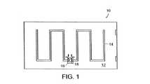
ここでは、通常のチップの向き(接合パッドが上方)及び裏返しのチップの向き(接合パッドが下方)のシリコンダイを考慮した本発明の2種の実施例が与えられる。図1はRFIDタグ10の平面図を示す。RFIDタグ10は、基板12及び基板12上に置かれたアンテナ14を備える。RFIDタグ10は、更にダイ位置決め構造16を備え、この中にシリコンダイ18が配置される。 Here, two embodiments of the present invention are given that consider silicon dies with normal chip orientation (bond pad up) and flipped chip orientation (bond pad down). FIG. 1 shows a plan view of the
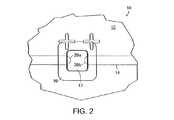
RFIDタグ10の詳細が、本発明の詳細平面図である図2に示される。図2に示されるように、ダイ位置決め構造16は、これがアンテナ14と重なるように基板12上に配置される。ダイ位置決め構造16は、これがアンテナのリード20a、20bと実質的に重なるように配置される。ダイ位置決め構造16は、一部にダイ位置決め用のキャビティ17を定め、これも、アンテナリード20a、20bの一方又は両方を、図4に示されるようなダイ接合パッド19、19Bへの接合のために利用できるようにアンテナリードと実質的に重なるように置かれる。 Details of the
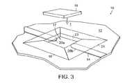
図3は、本発明の好ましい実施例によるRFIDタグ10の透視図である。図3に示されるように、ダイ位置決め構造16は外側スロープ21及び内側スロープ23を部分的に定める。更に、ダイ位置決め構造16は、これがアンテナ14と重なるように基板12上に配置されることが好ましい。ダイ位置決め構造16は、これがアンテナリード20a、20bと実質的に重なり更にダイ位置決めキャビティ17がアンテナリード20a、20bと実質的に重なるように配置される。ダイ位置決めキャビティ17はシリコンダイ18を受け入れるようにされ、このシリコンダイは矢印1の方向でダイ位置決めキャビティ17内に落とされる。 FIG. 3 is a perspective view of an
図4は、導電性でありかつRFIDタグ10の部分として示されたアンテナリード20a、20bに電気的に接続される1対の接点19a、19bを示しているシリコンダイ18の斜め方向透視図である。 4 is an oblique perspective view of the
図5は、本発明によるRFIDタグ10の断面図である。好ましい実施例においては、ダイ位置決め構造16はダイ位置決めキャビティ17を定める。ダイ位置決めキャビティ17は、基板12の表面に関して角度を付けられた内側スロープ23を定める。特に、基板12の表面に直角に第1の線Aが定められる。内側スロープ23の表面と同一面に第2の線Bが定められ、そしてAとBとの間の角度がαで示される。好ましい実施例においては、角度αは10゜から20゜の間であり、最も好ましくは約15゜である。内側スロープ23の傾斜面のため、シリコンダイ18をダイ位置決めキャビティ17内に位置決めするときの改良された信頼性と正確さとが許される。 FIG. 5 is a cross-sectional view of an
ダイ位置決め構造16は、基板12の表面に関して緩やかな角度の付けられた少なくも1個の外側面21も定める。外側面21の表面と同一面に第3の線Cが定められる。基板12の表面と同一面に第4の線Dが定められ、CとDとの間の角度がβで示される。好ましい実施例においては、角度βは20゜から40゜の間であり、最も好ましくは約30゜である。外側表面21の斜面のため、RFIDタグ10又は後のコーティング及び印刷ロールの摩耗及び裂けに対する抵抗を改善でき、そして何かの専断力又は摩擦がシリコンダイ18からアンテナ14への接続を移動させる可能性を減らすであろう。 The
RFIDタグ10は、図5に示されるように、ダイ位置決めキャビティ17内に、シリコンダイ18より前に下方充填材24が配置される別の実施例に対しても提供する。この場合、シリコンダイ18は、接合部26a、26bにおいてダイ位置決め構造16に接合され、これがアンテナ14に導電接続される。RFIDタグ10の弾性及び耐摩耗性を向上させるために、ダイ位置決め構造16、シリコンダイ18、及び接合部26a、26b上に、好ましくは非導電性材料で作られた保護キャップ22が配置される。好ましくは、保護キャップ22は、紫外線の作用からダイを光学的に遮蔽するために阻止用材料で処理される。 The
図1−5をまとめて参照し、好ましい実施例におけるRFIDタグ10が説明される。RFIDタグ10のアンテナ14は、金属又は合金のような導電性材料から作られる。ア
ンテナ用として普通に使用される金属は、例えば、金、銅、銀、アルミニウム、亜鉛、又はタングステンを含む。より好ましい実施例においては、アンテナ14は、金、銅、銀、又はアルミニウムの内の一つである。アンテナ14は、電子ビーム放射に対する阻止能の低いものであることが好ましい適切な基板12上に印刷され又は予め作られることが好ましい。Referring collectively to FIGS. 1-5, the
RFIDタグ10を選択する用途の形式がアンテナ14の仕様を定める。一実施例においては、アンテナ14は、400から1000メガヘルツの周波数範囲にわたり機能することができる。別の実施例においては、アンテナは915から920メガヘルツにわたる周波数範囲で機能することができる。より低い周波数の無線通信が普通である用途に対しては、アンテナ14は100から150キロヘルツの周波数範囲で機能できる。周波数の高い用途に対しては、アンテナ14は13.56メガヘルツで機能できる。欧州のような割り当て周波数の異なる諸外国での使用に対しては、アンテナ14は868から869メガヘルツの周波数範囲にわたり機能することができる。しかし、日本においては、950から960メガヘルツの間で機能するアンテナ14が提案される。ある種の用途に対しては、アンテナ14は、2.4から2.5ギガヘルツの周波数範囲にわたり機能することができる。RFIDタグ10用に選定されるアンテナ14の形式は、政府の割り当て権限及び特定用途に要求される信号の形式を含んだ多くの要因に依存するであろうことは明らかである。 The type of application for selecting the
基板12はかなり多くの材料のいずれとすることもできるが、最も好ましくは、ポリイミド、ポリエスエル、ポリエチレン、ポリプロピレン、木綿とポリエステルとの混合物、押出しコート紙、含浸紙、又はサーマルラベルを含んだ材料グループから選定される。注意されるように、基板12は、好ましくは、電子ビーム輻射に対する阻止能が低く、かつ広範囲の商業的使用をカバーし、更に複数のパッキングオプションに適合すべきである。基板12は、これらの条件を満たすために、厚さが好ましくは0.0025から0.0125cmであり、従って電子ビーム放射が容易に透過することができる。より好ましい実施例においては、基板12は厚さ0.005から0.010cmであり、より好ましい実施例においては、基板12は厚さ0.006から0.008cmである。 The
ダイ位置決め構造16は、電子ビーム放射により固化される非導電性又は誘電性材料より構成される。電子ビーム放射は、管理された照射量でポリマー材料に重合及び架橋反応を開始させるためのイオン化放射線として高エネルギー電子を使用する熱を使用しない方法である。電子固化は数十年間、変換産業において、典型的には薄膜、コーティング、又は積層用粘着剤の高速固化のために使用されてきた。ある種のポリマー(例えば、ポリエチレン)は電子ビーム処理によりそのままで固化するが、最も高性能のエポキシ及びアクリル共重合体のようなその他のものは固化を開始するための改変を必要とする。紫外線放射により追加の重合を開始することができるように光イニシエーターの追加により改変されたエポキシが、典型的な熱固化のものに匹敵する電気的及び熱機械的の特性を達成できることが示されている。 The
電子ビーム固化法は、通常の熱固化法に勝る次の諸点を含んだ幾つかの利点を持つ。即ち、製品の品質/性能の改良;環境、安全、及び健康に関する問題点の縮減;改良された材料の取り扱い;種々の材料及び機能を単一の作動に組み合わせる能力;他の方法では作ることのできない特有の部品を作る能力;消費エネルギーの減少;及び硬化時間の短縮の諸点である。本発明の文脈においては、特に重要な利点は、ほぼ室温で固化する性能である。接合パッドを基板に連結するための現在の熱固化技術は、150から160℃の範囲の温度に数秒間暴露することが必要である。電子ビーム固化を使用してこれを室温で迅速に行い得る事実により、上述のような熱に不安定な基板(例えば、コート紙又は含浸紙或いはポリマー薄膜)の使用を可能とする。エポキシ・テクノロジー(ビレリカ、マサチュ
ーセッツMA 01821)は、改変されたとき、電子ビーム固化法と関連した使用に適するであろうUV硬化可能な接着剤として説明された一連の製品を提案する。より特別には、電子ビーム固化法に関連して使用するために、UV硬化可能な接着剤から光イニシエーターを除去することができる。本技術熟練者はその他の適切な電子ビーム固化の可能なポリマー処方に慣れているであろう。The electron beam solidification method has several advantages over the normal thermal solidification method, including the following points. Improved product quality / performance; reduced environmental, safety, and health issues; improved material handling; ability to combine various materials and functions into a single operation; Ability to make unique parts that cannot be done; reduced energy consumption; and reduced cure time. In the context of the present invention, a particularly important advantage is the ability to solidify at about room temperature. Current thermal solidification techniques for bonding bond pads to substrates require exposure to temperatures in the range of 150 to 160 ° C. for several seconds. The fact that this can be done quickly at room temperature using electron beam solidification allows the use of thermally unstable substrates such as those described above (eg coated paper or impregnated paper or polymer films). Epoxy Technology (Billerica, Massachusetts MA 01821) proposes a series of products described as UV curable adhesives that, when modified, would be suitable for use in conjunction with electron beam solidification methods. More specifically, the photoinitiator can be removed from the UV curable adhesive for use in connection with the electron beam solidification method. Those skilled in the art will be familiar with other suitable electron beam solidifiable polymer formulations.
好ましい実施例においては、ダイ位置決め構造16は疎水性の材料より構成され、このためシリコンダイ18を着座させ、同時にRFIDタグ10の作動による電磁的及又は水分に原因する干渉を防ぐことができる。適切な材料は、電子ビーム放射に暴露されたときに迅速な重合化を受ける樹脂及びエポキシを含む。裏返しチップ(接合パッドが下側)の実施例においては、ダイ位置決め構造16は強力な絶縁体であることが好ましい。好ましい絶縁材料はアクリルウレタンであり、これは、基板14に適正に接合するために必要な接着特性を有するとともに、シリコンダイ18を受け入れるための適切な程度の柔軟性を維持する。図5に示される通常の(接合パッドが上側)の実施例においては、ダイ位置決め構造16は導電性であって、シリコンダイ18と基板12上に配置されたアンテナ14との間の容易な接続を許す。この実施例においては、ダイ位置決め構造16は、抵抗を減らすために十分な量の金属粉を加え又はドープした高度に導電性のエポキシであることが好ましい。上述された各実施例において、ダイ位置決め構造16は、シリコンダイ18を光起電力の作用から光学的に遮蔽するために遮光用顔料で処理される。 In the preferred embodiment, the
シリコンダイ18は、ある周波数範囲にわたり機能し得るアンテナ14への結合に適したシリコンダイのググループから選定される。一実施例においては、シリコンダイ18は、読出し専用メモリ(ROM)、電気的プログラム可能読出し専用メモリ(EPROM)、及び電気的消去及びプログラム可能読出し専用メモリ(EEPROM)よりなるグループから選定される。 Silicon die 18 is selected from a group of silicon dies suitable for coupling to
本発明の第2の態様は、上に詳述された改良されたRFIDタグ10を作る方法である。図6は、本発明の好ましい実施例によるRFIDタグ10の製造方法を示す流れ図である。 A second aspect of the present invention is a method of making the
本発明の方法は、ステップS110から出発し、ステップS112において選定された基板12を提供する。上述のように、基板12は、RFIDタグ10に関連して多くの適宜の材料のものとなし得るが、最も好ましくは、ポリイミド、ポリエスエル、ポリエチレン、ポリプロピレン、木綿とポリエステルとの混合物、押出しコート紙、含浸紙、又はサーマルラベルを含んだ材料グループから選定される。 The method of the present invention starts from step S110 and provides the
先に注意されたように、基板12は、電子ビーム放射を吸収することが少なく、更に広範囲の商業的な使用をカバーする複数のパッキングオプションに適合可能であるべきである。基板12は、これらの条件を満たすために、好ましくは厚さ0.0025から0.0125cmの間であり、従ってこれは電子ビーム放射が容易に透過することができる。より好ましい実施例においては、基板12は、厚さ0.005から0.010cmの間であり、より好ましい実施例においては、基板12は、厚さ0.006から0.008cmの間である。基板12はその上に置かれたアンテナ14を有し、或いは前述と同様なアンテナ14を受け入れるようにされることが好ましい。 As noted above, the
ステップS114において、上述のダイ位置決め構造16としての使用に適した第2の材料が選定される。ダイ位置決め構造16は、電子ビーム放射により硬化可能な絶縁材料又は誘電性材料より構成される。ダイ位置決め構造16は、疎水性でかつシリコンダイ18を確実に着座させ得ると同時にRFIDタグ10の作動による電磁的又は水分の干渉を防ぐものであることが好ましい。最後に、ダイ位置決め構造16は、シリコンダイ18を、光電作用から光学的に遮蔽するために阻止用顔料で処理されることが好ましい。 In step S114, a second material suitable for use as the
ステップS116において、第2の材料が基板とネガティブキャスト(negative cast)との間に配置されるようにダイ位置決め構造のネガティブキャストが位置決めされ、ダイ位置決め構造16が、第2の材料による彫り部分(ネガティブキャスト)の充填に続いて形成されるであろう。ステップS118。 In step S116, the negative cast of the die positioning structure is positioned such that the second material is disposed between the substrate and the negative cast, and the
ステップS118において第2の材料がダイ位置決め構造16内に押し込まれると、第2の材料がステップS120において固化される。固化ステップは、第2の材料を重合させそしてダイ位置決め構造16にするための電子ビームの放射の使用を含む。好ましい実施例においては、第2の材料の固化のステップは、100から300キロ電子ボルト(keV)の範囲のエネルギーを有する電子ビームの使用を含む。最も好ましくは、固化用電子ビームのエネルギーは約200keVである。 When the second material is pushed into the
ステップS120における第2の材料の電子ビーム固化に続いて、ステップS122においてシリコンダイ18がダイ位置決め構造16及びアンテナ14に接合される。次いで、ステップS123においてサンプル無線信号を提供してRFIDタグ10の応答を測定することにより、RFIDタグ10の機能を検査することができる。 Following the electron beam solidification of the second material in step S120, the silicon die 18 is bonded to the die
RFIDタグ10が検査に合格した後、ステップS124においてシリコンダイ18及びダイ位置決め構造16の上に保護コーティングが置かれる。RFIDタグ10の信頼性の向上のために、保護層22は好ましくは非導電性材料から構成され、そしてダイ位置決め構造16、シリコンダイ18、及び接合部26a、26b上に置かれる。好ましくは、保護層22は、シリコンダイ18を光電気作用から光学的に遮蔽するために阻止用顔料で処理される。ステップS126は、改良されたRFIDタグ10の製造方法の終わりを表すが、この方法は、多くの商業的企業にわたる使用に対して適切なRFIDタグの大量のストックを作るために連続して繰り返されることが理解される。 After the
本発明のRFIDタグ10の製造方法は、これを作る方法を成し遂げるシステムを関連して説明することもできる。図7は、基板12及びダイ位置決め構造16としての使用に適した第2の材料15を含んだRFIDタグ10の一製造方法の略図である。この方法の実施例においては、第2の材料15に直接隣接してネガティブキャスト50が示される。基板12、第2の材料15、及びネガティブキャスト50の上方にプレス機構60が配置される。プレス機構60は、第2の材料15がシステムを通過できるようにネガティブキャスト50に関して移動可能であり、或いはプレス機構60をネガティブキャスト50に関して固定することができる。 The manufacturing method of the
図7に示されるように、プレス機構60は矢印2に沿って中央軸線に沿って回転することができる。ネガティブキャスト50は、プレス機構60が常に新しい材料をネガティブキャスト50内に押し込むように、矢印3に沿って移動可能である。この方法のプレス段階に続いて、上述のようにダイ位置決め構造16内に第2の材料15を固化させる電子ビーム64を作るために電子ビーム発生器62が提供される。好ましい実施例においては、電子ビームは、100から300キロ電子ボルト(keV)の範囲のエネルギーを持つ。最も好ましくは、固化用電子ビームのエネルギーは約200keVである。 As shown in FIG. 7, the
図8は、RFIDタグ10の製造に使用し得る好ましいネガティブキャスト50の断面図である。図9は、好ましいネガティブキャスト50の平面図である。ネガティブキャスト50により定められる形状は、上に詳細説明されたダイ位置決め構造16により定められる形状の逆である。ネガティブキャスト50は、内側バンク54と外側バンク52とを定める。ネガティブキャスト50の表面に直角に線Eが定められる。内側バンク54の表
面と同一面に線Fが定められ、そして線EとFとの間の角度がδで示される。角度δは、好ましくは10゜から20゜の間であり、そして最も好ましくは約15゜である。FIG. 8 is a cross-sectional view of a preferred
ネガティブキャスト50の外側バンク52は、図3に示された特徴の外側バンク21を有するダイ位置決め構造16を鋳造するために、より緩やかな傾斜にされる。ネガティブキャスト50と同一平面として線Hが定められる。外側バンク52と同一平面として線Gが定められ、そして線GとHとの間の角度がφで示される。角度φは、好ましくは20゜と40゜との間であり、そして最も好ましくは約30゜である。 The
図10は、本発明により基板上のダイ位置決めシステムを作る方法70の略図である。方法70のこの図式表現は、この特許の請求範囲を限定することを意図するものではなく本発明によるRFIDタグ10の体系的な製造方法の例として意図されたものである。 FIG. 10 is a schematic diagram of a
方法70の一実施例においては、基板12は、中心軸線まわりに矢印4の方向で回転する第1のシリンダー72上に連続的に供給される。第1のシリンダー72は、タグの大きさに適合したシーケンスでその表面上に配置された複数個のネガティブキャスト50を持つ。第2の材料15が、液状でパン78内に配置される。矢印5及び6で示された反対方向に回転し得る第2のシリンダー80a(彫られたものであることが普通)及び第3のシリンダー80b(典型的にはゴムロール)が、第2の材料15をパン78から取り出してこれを第1のシリンダー72に供給する。ドクターブレード82が、余分の第2の材料がないように第1のシリンダー72を清掃する。 In one embodiment of the
基板12が第2の材料15上に置かれる。矢印7の方向で回転できる第4のシリンダー74が、第2の材料15を第1のシリンダー72の表面上のネガティブキャスト50内に押し込むように作用する。上述のように、第2の材料15をダイ位置決め構造16内に固化させる電子ビーム64を作るために、第1のシリンダー72からある距離に電子ビーム発生器62が配置される。好ましい実施例においては、電子ビームは100から300キロ電子ボルト(keV)のエネルギーを持つ。最も好ましくは、固化用電子ビームのエネルギーは約200keVである。固化後、第5のシリンダー76が第1のシリンダー72から固化された第2の材料15を取り外す。上述のように、この新たに形成されたダイ位置決め構造16及び基板12は、シリコンダイ18及びここに請求される残りの諸ステップを受け入れるようにされる。 A
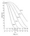
図11は、電子ビームのエネルギーの関数としての侵入レンジ(グラム/m2)と線量侵入パーセント(%)との間の関係を示すグラフである。先に注意されたように、第2の材料15をダイ位置決め構造16内に固化させる電子ビーム64を作るために電子ビーム発生器62が利用される。好ましい実施例においては、電子ビームは、100から300キロ電子ボルト(keV)のエネルギーを持つ。最も好ましくは、固化用電子ビームのエネルギーは約200keVである。FIG. 11 is a graph showing the relationship between penetration range (grams / m2 ) and dose penetration percentage (%) as a function of electron beam energy. As noted above, an
好ましい実施例について説明された本発明は、新規なRFIDタグについての特定の製造方法の提供に加えてRFIDタグの製造の手順を改良する。特に、選定された材料における体系的かつ信頼できる手段によるダイ位置決め構造の形成が、より信頼でき弾性的なRFIDタグを提供するであろう。更に、電子ビーム固化により、ダイ位置決め構造、RFIDタグの製造速度を非常に増大させ、RFIDタグの商業用分野の拡大を許すことができる。 The invention described for the preferred embodiment improves the RFID tag manufacturing procedure in addition to providing a specific manufacturing method for the new RFID tag. In particular, the formation of die positioning structures by systematic and reliable means in selected materials will provide a more reliable and elastic RFID tag. Furthermore, the solidification of the electron beam can greatly increase the die positioning structure and the manufacturing speed of the RFID tag, allowing the commercial field of the RFID tag to be expanded.
上述の諸実施例は、単に説明のためのものであり、本発明の多くの可能な特別の実施例の内の数例にすぎないことが本技術熟練者には明らかであろう。これら熟練技術者は、特許請求の範囲に定められた本発明の精神及び範囲から離れることなく、多種多数の配列を
考えることができる。It will be apparent to those skilled in the art that the above-described embodiments are merely illustrative and are just a few of the many possible specific embodiments of the present invention. Those skilled in the art can envision many different arrangements without departing from the spirit and scope of the invention as defined in the claims.
Claims (51)
Translated fromJapanese基板上に配置されたアンテナ;
基板上に配置されかつシリコンダイを受け入れるためのキャビティを定めているダイ位置決め構造;及び
ダイ位置決め構造内に配置されたシリコンダイであて、アンテナへの接続のために少なくも1個の接合部を有するシリコンダイ
を備えた無線周波識別(RFID)タグ。Substrate material;
An antenna placed on a substrate;
A die positioning structure disposed on a substrate and defining a cavity for receiving a silicon die; and a silicon die disposed within the die positioning structure, wherein at least one junction is provided for connection to an antenna. A radio frequency identification (RFID) tag comprising a silicon die.
基板上の予備成型されたアンテナを提供し;
第2の材料を提供し;
ダイ位置決め構造のネガティブキャストを提供し;
基板とネガティブキャストとの間で第2の材料をプレスし、これによりダイ位置決め構造を提供し;
第2の材料を固化し、これにより固化されたダイ位置決め構造を提供し;更に
シリコンダイを固化されたダイ位置決め構造内に固定する
ことを含んだ無線周波識別(RFID)タグの製造方法。Providing a substrate;
Providing a preformed antenna on the substrate;
Providing a second material;
Provide negative cast of die positioning structure;
Pressing a second material between the substrate and the negative cast, thereby providing a die positioning structure;
A method of manufacturing a radio frequency identification (RFID) tag comprising solidifying a second material, thereby providing a solidified die positioning structure; and further securing a silicon die within the solidified die positioning structure.
Applications Claiming Priority (2)
| Application Number | Priority Date | Filing Date | Title |
|---|---|---|---|
| US10/958,699US7221277B2 (en) | 2004-10-05 | 2004-10-05 | Radio frequency identification tag and method of making the same |
| PCT/US2005/030163WO2006041576A1 (en) | 2004-10-05 | 2005-08-22 | Radio frequency identification tag and method of making the same |
Publications (2)
| Publication Number | Publication Date |
|---|---|
| JP2008516525Atrue JP2008516525A (en) | 2008-05-15 |
| JP2008516525A5 JP2008516525A5 (en) | 2008-10-09 |
Family
ID=36124993
Family Applications (1)
| Application Number | Title | Priority Date | Filing Date |
|---|---|---|---|
| JP2007535679APendingJP2008516525A (en) | 2004-10-05 | 2005-08-22 | Radio frequency identification tag and manufacturing method thereof |
Country Status (5)
| Country | Link |
|---|---|
| US (2) | US7221277B2 (en) |
| EP (1) | EP1797540A4 (en) |
| JP (1) | JP2008516525A (en) |
| CA (1) | CA2582671A1 (en) |
| WO (1) | WO2006041576A1 (en) |
Cited By (3)
| Publication number | Priority date | Publication date | Assignee | Title |
|---|---|---|---|---|
| WO2021065949A1 (en)* | 2019-09-30 | 2021-04-08 | 京セラ株式会社 | Optical waveguide package and light emitting device |
| WO2021065948A1 (en)* | 2019-09-30 | 2021-04-08 | 京セラ株式会社 | Optical waveguide package and light emitting device |
| US12181723B2 (en) | 2019-09-30 | 2024-12-31 | Kyocera Corporation | Optical waveguide package and light-emitting device |
Families Citing this family (48)
| Publication number | Priority date | Publication date | Assignee | Title |
|---|---|---|---|---|
| JP2005216077A (en)* | 2004-01-30 | 2005-08-11 | Bridgestone Corp | Bar code label with built-in rfid, tire and management method therefor |
| US20060131709A1 (en)* | 2004-12-21 | 2006-06-22 | Caron Michael R | Semiconductor die positioning system and a method of bonding a semiconductor die to a substrate |
| AU2005322072A1 (en) | 2004-12-27 | 2006-07-06 | Quantum Paper, Inc. | Addressable and printable emissive display |
| US20110175343A1 (en)* | 2005-01-31 | 2011-07-21 | Pipe Maintenance, Inc. | Identification system for drill pipes and the like |
| US7659857B2 (en)* | 2006-07-05 | 2010-02-09 | King Patrick F | System and method for providing a low and narrow-profile radio frequency identification (RFID) tag |
| US9652707B2 (en) | 2006-10-31 | 2017-05-16 | Fiber Mountain, Inc. | Radio frequency identification (RFID) connected tag communications protocol and related systems and methods |
| US8264366B2 (en)* | 2009-03-31 | 2012-09-11 | Corning Incorporated | Components, systems, and methods for associating sensor data with component location |
| US9652709B2 (en) | 2006-10-31 | 2017-05-16 | Fiber Mountain, Inc. | Communications between multiple radio frequency identification (RFID) connected tags and one or more devices, and related systems and methods |
| US7772975B2 (en)* | 2006-10-31 | 2010-08-10 | Corning Cable Systems, Llc | System for mapping connections using RFID function |
| US7782202B2 (en) | 2006-10-31 | 2010-08-24 | Corning Cable Systems, Llc | Radio frequency identification of component connections |
| US8421626B2 (en)* | 2006-10-31 | 2013-04-16 | Corning Cable Systems, Llc | Radio frequency identification transponder for communicating condition of a component |
| US9652708B2 (en) | 2006-10-31 | 2017-05-16 | Fiber Mountain, Inc. | Protocol for communications between a radio frequency identification (RFID) tag and a connected device, and related systems and methods |
| US10032102B2 (en) | 2006-10-31 | 2018-07-24 | Fiber Mountain, Inc. | Excess radio-frequency (RF) power storage in RF identification (RFID) tags, and related systems and methods |
| US7760094B1 (en) | 2006-12-14 | 2010-07-20 | Corning Cable Systems Llc | RFID systems and methods for optical fiber network deployment and maintenance |
| US7667574B2 (en)* | 2006-12-14 | 2010-02-23 | Corning Cable Systems, Llc | Signal-processing systems and methods for RFID-tag signals |
| US8264355B2 (en) | 2006-12-14 | 2012-09-11 | Corning Cable Systems Llc | RFID systems and methods for optical fiber network deployment and maintenance |
| US7547150B2 (en)* | 2007-03-09 | 2009-06-16 | Corning Cable Systems, Llc | Optically addressed RFID elements |
| US7965186B2 (en) | 2007-03-09 | 2011-06-21 | Corning Cable Systems, Llc | Passive RFID elements having visual indicators |
| US8846457B2 (en) | 2007-05-31 | 2014-09-30 | Nthdegree Technologies Worldwide Inc | Printable composition of a liquid or gel suspension of diodes |
| US8674593B2 (en) | 2007-05-31 | 2014-03-18 | Nthdegree Technologies Worldwide Inc | Diode for a printable composition |
| US8809126B2 (en) | 2007-05-31 | 2014-08-19 | Nthdegree Technologies Worldwide Inc | Printable composition of a liquid or gel suspension of diodes |
| US9343593B2 (en) | 2007-05-31 | 2016-05-17 | Nthdegree Technologies Worldwide Inc | Printable composition of a liquid or gel suspension of diodes |
| US8852467B2 (en) | 2007-05-31 | 2014-10-07 | Nthdegree Technologies Worldwide Inc | Method of manufacturing a printable composition of a liquid or gel suspension of diodes |
| US9018833B2 (en) | 2007-05-31 | 2015-04-28 | Nthdegree Technologies Worldwide Inc | Apparatus with light emitting or absorbing diodes |
| US8889216B2 (en) | 2007-05-31 | 2014-11-18 | Nthdegree Technologies Worldwide Inc | Method of manufacturing addressable and static electronic displays |
| US8133768B2 (en) | 2007-05-31 | 2012-03-13 | Nthdegree Technologies Worldwide Inc | Method of manufacturing a light emitting, photovoltaic or other electronic apparatus and system |
| US9534772B2 (en) | 2007-05-31 | 2017-01-03 | Nthdegree Technologies Worldwide Inc | Apparatus with light emitting diodes |
| US9425357B2 (en) | 2007-05-31 | 2016-08-23 | Nthdegree Technologies Worldwide Inc. | Diode for a printable composition |
| US8877101B2 (en) | 2007-05-31 | 2014-11-04 | Nthdegree Technologies Worldwide Inc | Method of manufacturing a light emitting, power generating or other electronic apparatus |
| US8384630B2 (en) | 2007-05-31 | 2013-02-26 | Nthdegree Technologies Worldwide Inc | Light emitting, photovoltaic or other electronic apparatus and system |
| US8415879B2 (en) | 2007-05-31 | 2013-04-09 | Nthdegree Technologies Worldwide Inc | Diode for a printable composition |
| US9419179B2 (en) | 2007-05-31 | 2016-08-16 | Nthdegree Technologies Worldwide Inc | Diode for a printable composition |
| US7855697B2 (en)* | 2007-08-13 | 2010-12-21 | Corning Cable Systems, Llc | Antenna systems for passive RFID tags |
| US7992332B2 (en) | 2008-05-13 | 2011-08-09 | Nthdegree Technologies Worldwide Inc. | Apparatuses for providing power for illumination of a display object |
| US8127477B2 (en) | 2008-05-13 | 2012-03-06 | Nthdegree Technologies Worldwide Inc | Illuminating display systems |
| US8248208B2 (en) | 2008-07-15 | 2012-08-21 | Corning Cable Systems, Llc. | RFID-based active labeling system for telecommunication systems |
| US8731405B2 (en) | 2008-08-28 | 2014-05-20 | Corning Cable Systems Llc | RFID-based systems and methods for collecting telecommunications network information |
| EP2507746B1 (en) | 2009-11-30 | 2015-10-14 | Corning Incorporated | Rfid condition latching |
| US9122967B2 (en) | 2010-04-14 | 2015-09-01 | Technologies Roi, Llc | Radio frequency identification tags and methods employing ceramic components, which may be suitable for use in extreme environmental conditions |
| US8172468B2 (en) | 2010-05-06 | 2012-05-08 | Corning Incorporated | Radio frequency identification (RFID) in communication connections, including fiber optic components |
| EP2453264B1 (en)* | 2010-11-10 | 2021-09-01 | Elydan | Polymer tube comprising an identification sensor and method for manufacturing same |
| USD678227S1 (en)* | 2011-03-07 | 2013-03-19 | Ricoh Company, Ltd. | Tag for removable part |
| US9165232B2 (en) | 2012-05-14 | 2015-10-20 | Corning Incorporated | Radio-frequency identification (RFID) tag-to-tag autoconnect discovery, and related methods, circuits, and systems |
| US9563832B2 (en) | 2012-10-08 | 2017-02-07 | Corning Incorporated | Excess radio-frequency (RF) power storage and power sharing RF identification (RFID) tags, and related connection systems and methods |
| CN103022683A (en)* | 2013-01-06 | 2013-04-03 | 北京邮电大学 | Double-face superminiature UHF RFID (ultra high frequency radio frequency identification) tag antenna derived from ENG (electronic news gathering) material |
| US10176422B2 (en)* | 2015-06-09 | 2019-01-08 | Assa Abloy Ab | RIFD tag with a tunable antenna |
| US10320054B2 (en)* | 2016-10-28 | 2019-06-11 | Avery Dennison Retail Information Services, Llc | RFID tags designed to work on difficult substrates |
| US10296821B2 (en) | 2017-08-17 | 2019-05-21 | Assa Abloy Ab | RFID devices and methods of making the same |
Citations (7)
| Publication number | Priority date | Publication date | Assignee | Title |
|---|---|---|---|---|
| JPH0566330A (en)* | 1990-09-28 | 1993-03-19 | Toshiba Corp | Semiconductor module |
| JPH0885285A (en)* | 1994-07-21 | 1996-04-02 | Hitachi Maxell Ltd | Security card substrate manufacturing method and security card substrate |
| JPH11353439A (en)* | 1998-06-04 | 1999-12-24 | Dainippon Printing Co Ltd | Non-contact IC card, method of manufacturing the same, base for non-contact IC card |
| US6375780B1 (en)* | 1992-06-17 | 2002-04-23 | Micron Technology, Inc. | Method of manufacturing an enclosed transceiver |
| US20030136503A1 (en)* | 2002-01-18 | 2003-07-24 | Avery Dennison Corporation | RFID label technique |
| JP2004078991A (en)* | 1998-12-17 | 2004-03-11 | Hitachi Ltd | Semiconductor device and method of manufacturing the same |
| JP2004509479A (en)* | 2000-09-19 | 2004-03-25 | ナノピアス・テクノロジーズ・インコーポレイテッド | Method for assembling a plurality of components and a plurality of antennas in a radio frequency identification device |
Family Cites Families (29)
| Publication number | Priority date | Publication date | Assignee | Title |
|---|---|---|---|---|
| US3480836A (en)* | 1966-08-11 | 1969-11-25 | Ibm | Component mounted in a printed circuit |
| US4023482A (en)* | 1974-09-23 | 1977-05-17 | Litton Business Systems, Inc. | Printing of automatically readable characters |
| US4840757A (en)* | 1987-05-19 | 1989-06-20 | S. D. Warren Company | Replicating process for interference patterns |
| JP2558744B2 (en)* | 1987-10-08 | 1996-11-27 | シャープ株式会社 | Semiconductor laser device and manufacturing method thereof |
| US5034802A (en)* | 1989-12-11 | 1991-07-23 | Hewlett-Packard Company | Mechanical simultaneous registration of multi-pin surface-mount components to sites on substrates |
| US5205032A (en)* | 1990-09-28 | 1993-04-27 | Kabushiki Kaisha Toshiba | Electronic parts mounting apparatus |
| US5776278A (en)* | 1992-06-17 | 1998-07-07 | Micron Communications, Inc. | Method of manufacturing an enclosed transceiver |
| US5296736A (en)* | 1992-12-21 | 1994-03-22 | Motorola, Inc. | Leveled non-coplanar semiconductor die contacts |
| EP0622858B2 (en)* | 1993-04-28 | 2004-09-29 | Nichia Corporation | Gallium nitride-based III-V group compound semiconductor device and method of producing the same |
| US5545291A (en)* | 1993-12-17 | 1996-08-13 | The Regents Of The University Of California | Method for fabricating self-assembling microstructures |
| US5965867A (en)* | 1996-07-19 | 1999-10-12 | Gieseke & Devrient Gmbh | Data medium incorporating integrated circuits |
| US6194317B1 (en)* | 1998-04-30 | 2001-02-27 | 3M Innovative Properties Company | Method of planarizing the upper surface of a semiconductor wafer |
| US5955949A (en)* | 1997-08-18 | 1999-09-21 | X-Cyte, Inc. | Layered structure for a transponder tag |
| US6102777A (en)* | 1998-03-06 | 2000-08-15 | Keltech Engineering | Lapping apparatus and method for high speed lapping with a rotatable abrasive platen |
| US6121878A (en)* | 1998-05-01 | 2000-09-19 | Intermec Ip Corp. | System for controlling assets |
| US6018299A (en)* | 1998-06-09 | 2000-01-25 | Motorola, Inc. | Radio frequency identification tag having a printed antenna and method |
| US6246327B1 (en)* | 1998-06-09 | 2001-06-12 | Motorola, Inc. | Radio frequency identification tag circuit chip having printed interconnection pads |
| US6515586B1 (en)* | 1998-12-18 | 2003-02-04 | Intel Corporation | Tactile tracking systems and methods |
| US6366468B1 (en)* | 2000-04-28 | 2002-04-02 | Hewlett-Packard Company | Self-aligned common carrier |
| BRPI0112645B1 (en)* | 2000-07-19 | 2016-07-05 | Hanex Co Ltd | housing structure and installation structure for a radio frequency identification indicator and communication method using a radio frequency identification indicator |
| US6774766B1 (en)* | 2000-07-21 | 2004-08-10 | E-Tag Systems, Inc. | Method for efficiently querying and identifying multiple items on a communication channel |
| US6611237B2 (en)* | 2000-11-30 | 2003-08-26 | The Regents Of The University Of California | Fluidic self-assembly of active antenna |
| US6603403B2 (en)* | 2000-12-12 | 2003-08-05 | Kimberly-Clark Worldwide, Inc. | Remote, wetness signaling system |
| US20060071084A1 (en)* | 2000-12-15 | 2006-04-06 | Electrox Corporation | Process for manufacture of novel, inexpensive radio frequency identification devices |
| US6606247B2 (en)* | 2001-05-31 | 2003-08-12 | Alien Technology Corporation | Multi-feature-size electronic structures |
| FI112550B (en)* | 2001-05-31 | 2003-12-15 | Rafsec Oy | Smart label and smart label path |
| US7755484B2 (en)* | 2004-02-12 | 2010-07-13 | Avery Dennison Corporation | RFID tag and method of manufacturing the same |
| US7135973B2 (en)* | 2004-02-13 | 2006-11-14 | Avery Dennison Corporation | Tamper monitoring article, system and method |
| US7268687B2 (en)* | 2004-03-23 | 2007-09-11 | 3M Innovative Properties Company | Radio frequency identification tags with compensating elements |
- 2004
- 2004-10-05USUS10/958,699patent/US7221277B2/ennot_activeCeased
- 2005
- 2005-08-22JPJP2007535679Apatent/JP2008516525A/enactivePending
- 2005-08-22CACA002582671Apatent/CA2582671A1/ennot_activeAbandoned
- 2005-08-22EPEP05789873Apatent/EP1797540A4/ennot_activeWithdrawn
- 2005-08-22WOPCT/US2005/030163patent/WO2006041576A1/enactiveApplication Filing
- 2009
- 2009-03-03USUS12/396,691patent/USRE41563E1/ennot_activeExpired - Fee Related
Patent Citations (7)
| Publication number | Priority date | Publication date | Assignee | Title |
|---|---|---|---|---|
| JPH0566330A (en)* | 1990-09-28 | 1993-03-19 | Toshiba Corp | Semiconductor module |
| US6375780B1 (en)* | 1992-06-17 | 2002-04-23 | Micron Technology, Inc. | Method of manufacturing an enclosed transceiver |
| JPH0885285A (en)* | 1994-07-21 | 1996-04-02 | Hitachi Maxell Ltd | Security card substrate manufacturing method and security card substrate |
| JPH11353439A (en)* | 1998-06-04 | 1999-12-24 | Dainippon Printing Co Ltd | Non-contact IC card, method of manufacturing the same, base for non-contact IC card |
| JP2004078991A (en)* | 1998-12-17 | 2004-03-11 | Hitachi Ltd | Semiconductor device and method of manufacturing the same |
| JP2004509479A (en)* | 2000-09-19 | 2004-03-25 | ナノピアス・テクノロジーズ・インコーポレイテッド | Method for assembling a plurality of components and a plurality of antennas in a radio frequency identification device |
| US20030136503A1 (en)* | 2002-01-18 | 2003-07-24 | Avery Dennison Corporation | RFID label technique |
Cited By (6)
| Publication number | Priority date | Publication date | Assignee | Title |
|---|---|---|---|---|
| WO2021065949A1 (en)* | 2019-09-30 | 2021-04-08 | 京セラ株式会社 | Optical waveguide package and light emitting device |
| JPWO2021065949A1 (en)* | 2019-09-30 | 2021-04-08 | ||
| WO2021065948A1 (en)* | 2019-09-30 | 2021-04-08 | 京セラ株式会社 | Optical waveguide package and light emitting device |
| JPWO2021065948A1 (en)* | 2019-09-30 | 2021-04-08 | ||
| JP7300794B2 (en) | 2019-09-30 | 2023-06-30 | 京セラ株式会社 | Optical waveguide package and light emitting device |
| US12181723B2 (en) | 2019-09-30 | 2024-12-31 | Kyocera Corporation | Optical waveguide package and light-emitting device |
Also Published As
| Publication number | Publication date |
|---|---|
| EP1797540A4 (en) | 2009-07-08 |
| WO2006041576A1 (en) | 2006-04-20 |
| EP1797540A1 (en) | 2007-06-20 |
| US20060071792A1 (en) | 2006-04-06 |
| US7221277B2 (en) | 2007-05-22 |
| USRE41563E1 (en) | 2010-08-24 |
| CA2582671A1 (en) | 2006-04-20 |
Similar Documents
| Publication | Publication Date | Title |
|---|---|---|
| JP2008516525A (en) | Radio frequency identification tag and manufacturing method thereof | |
| US7576656B2 (en) | Apparatuses and methods for high speed bonding | |
| KR100846272B1 (en) | Rfid tag and manufacturing method thereof | |
| US20020179721A1 (en) | Electronic module or label with a fixing adhesive forming a barrier for coating resin, and a medium including a module or label of this kind | |
| US7951249B2 (en) | RFID tag | |
| JP3248518U (en) | Apparatus for forming labels with integrated conductive patterns - Patent Application 20070123633 | |
| US8009049B2 (en) | RFID tag and method of manufacturing RFID tag | |
| JP7503696B2 (en) | Antenna patterns, RFID inlays and RFID labels | |
| JP7154288B2 (en) | Method and apparatus for manufacturing radio frequency identification transponders | |
| JP2007157140A (en) | Wireless frequency wave device | |
| KR20070043635A (en) | RF antenna with pre-coated adhesive | |
| US20060290512A1 (en) | Methods and apparatus for RFID transponder fabrication | |
| EP3846082A1 (en) | Heat transfer rfid tag for fabric and method of manufacturing the same | |
| US20150122892A1 (en) | Radio frequency identification tag | |
| JP5116528B2 (en) | Method for manufacturing contactless data receiving / transmitting body | |
| JP7353578B2 (en) | IC tag | |
| US20060065738A1 (en) | Rfid device and method of manufacture | |
| JP7568186B2 (en) | RFID tags | |
| JP7293918B2 (en) | Manufacturing method of resonance identifier | |
| US20060131709A1 (en) | Semiconductor die positioning system and a method of bonding a semiconductor die to a substrate | |
| US20080012713A1 (en) | Method for Connecting a Bridge Module to a Substrate and Multi-Layer Transponder | |
| CA2528797A1 (en) | Rfid transponder structure optimized for in-line label construction | |
| JP2023107554A (en) | Container and method for manufacturing the container | |
| US20230237302A1 (en) | Ic tag and manufacturing method | |
| JP2011186946A (en) | Non-contact type data receiving and transmitting object |
Legal Events
| Date | Code | Title | Description |
|---|---|---|---|
| A521 | Request for written amendment filed | Free format text:JAPANESE INTERMEDIATE CODE: A523 Effective date:20080821 | |
| A621 | Written request for application examination | Free format text:JAPANESE INTERMEDIATE CODE: A621 Effective date:20080821 | |
| RD02 | Notification of acceptance of power of attorney | Free format text:JAPANESE INTERMEDIATE CODE: A7422 Effective date:20090115 | |
| A521 | Request for written amendment filed | Free format text:JAPANESE INTERMEDIATE CODE: A821 Effective date:20090115 | |
| A131 | Notification of reasons for refusal | Free format text:JAPANESE INTERMEDIATE CODE: A131 Effective date:20101005 | |
| A601 | Written request for extension of time | Free format text:JAPANESE INTERMEDIATE CODE: A601 Effective date:20110104 | |
| A602 | Written permission of extension of time | Free format text:JAPANESE INTERMEDIATE CODE: A602 Effective date:20110112 | |
| A02 | Decision of refusal | Free format text:JAPANESE INTERMEDIATE CODE: A02 Effective date:20110405 |