JP2008514984A - Method and device for suppressing mirror tilt in an interferometric modulator - Google Patents
Method and device for suppressing mirror tilt in an interferometric modulatorDownload PDFInfo
- Publication number
- JP2008514984A JP2008514984AJP2007533475AJP2007533475AJP2008514984AJP 2008514984 AJP2008514984 AJP 2008514984AJP 2007533475 AJP2007533475 AJP 2007533475AJP 2007533475 AJP2007533475 AJP 2007533475AJP 2008514984 AJP2008514984 AJP 2008514984A
- Authority
- JP
- Japan
- Prior art keywords
- mirror
- interferometric modulator
- substrate
- distance
- movement
- Prior art date
- Legal status (The legal status is an assumption and is not a legal conclusion. Google has not performed a legal analysis and makes no representation as to the accuracy of the status listed.)
- Granted
Links
- 238000000034methodMethods0.000titleclaimsabstractdescription42
- 230000003287optical effectEffects0.000claimsabstractdescription87
- 230000033001locomotionEffects0.000claimsabstractdescription62
- 230000006641stabilisationEffects0.000claimsabstract2
- 238000011105stabilizationMethods0.000claimsabstract2
- 239000000758substrateSubstances0.000claimsdescription59
- 230000000007visual effectEffects0.000claimsdescription11
- 230000008569processEffects0.000claimsdescription10
- 230000000087stabilizing effectEffects0.000claimsdescription8
- 230000036961partial effectEffects0.000claimsdescription4
- 230000005540biological transmissionEffects0.000claimsdescription3
- 230000001154acute effectEffects0.000claimsdescription2
- 238000007373indentationMethods0.000claimsdescription2
- 230000002401inhibitory effectEffects0.000claims1
- 239000000463materialSubstances0.000description29
- 238000010586diagramMethods0.000description11
- 238000013461designMethods0.000description9
- 238000004519manufacturing processMethods0.000description9
- 230000008901benefitEffects0.000description7
- 229910052751metalInorganic materials0.000description6
- 239000002184metalSubstances0.000description6
- 230000003750conditioning effectEffects0.000description5
- 230000008859changeEffects0.000description4
- 238000000151depositionMethods0.000description4
- 238000012545processingMethods0.000description4
- 238000013459approachMethods0.000description3
- 239000003990capacitorSubstances0.000description3
- 239000003086colorantSubstances0.000description3
- 230000008021depositionEffects0.000description3
- 238000005530etchingMethods0.000description3
- 239000011159matrix materialSubstances0.000description3
- 238000000059patterningMethods0.000description3
- VYZAMTAEIAYCRO-UHFFFAOYSA-NChromiumChemical compound[Cr]VYZAMTAEIAYCRO-UHFFFAOYSA-N0.000description2
- 229910052804chromiumInorganic materials0.000description2
- 239000011651chromiumSubstances0.000description2
- 239000010408filmSubstances0.000description2
- 230000004927fusionEffects0.000description2
- AMGQUBHHOARCQH-UHFFFAOYSA-Nindium;oxotinChemical compound[In].[Sn]=OAMGQUBHHOARCQH-UHFFFAOYSA-N0.000description2
- 230000002093peripheral effectEffects0.000description2
- 239000004033plasticSubstances0.000description2
- 230000002441reversible effectEffects0.000description2
- 238000000926separation methodMethods0.000description2
- 230000003068static effectEffects0.000description2
- IRLPACMLTUPBCL-KQYNXXCUSA-N5'-adenylyl sulfateChemical compoundC1=NC=2C(N)=NC=NC=2N1[C@@H]1O[C@H](COP(O)(=O)OS(O)(=O)=O)[C@@H](O)[C@H]1OIRLPACMLTUPBCL-KQYNXXCUSA-N0.000description1
- 235000001674Agaricus brunnescensNutrition0.000description1
- HBBGRARXTFLTSG-UHFFFAOYSA-NLithium ionChemical compound[Li+]HBBGRARXTFLTSG-UHFFFAOYSA-N0.000description1
- 230000009471actionEffects0.000description1
- 230000002411adverseEffects0.000description1
- 229910052782aluminiumInorganic materials0.000description1
- XAGFODPZIPBFFR-UHFFFAOYSA-NaluminiumChemical compound[Al]XAGFODPZIPBFFR-UHFFFAOYSA-N0.000description1
- 230000009286beneficial effectEffects0.000description1
- 230000015572biosynthetic processEffects0.000description1
- -1but not limited toSubstances0.000description1
- OJIJEKBXJYRIBZ-UHFFFAOYSA-Ncadmium nickelChemical compound[Ni].[Cd]OJIJEKBXJYRIBZ-UHFFFAOYSA-N0.000description1
- 230000001413cellular effectEffects0.000description1
- 239000004020conductorSubstances0.000description1
- 230000008878couplingEffects0.000description1
- 238000010168coupling processMethods0.000description1
- 238000005859coupling reactionMethods0.000description1
- 230000001066destructive effectEffects0.000description1
- 229910052571earthenwareInorganic materials0.000description1
- 230000000694effectsEffects0.000description1
- 238000004146energy storageMethods0.000description1
- 238000005516engineering processMethods0.000description1
- 239000011521glassSubstances0.000description1
- 238000001746injection mouldingMethods0.000description1
- 230000003993interactionEffects0.000description1
- 229910001416lithium ionInorganic materials0.000description1
- 238000003754machiningMethods0.000description1
- 239000012528membraneSubstances0.000description1
- 239000007769metal materialSubstances0.000description1
- 238000005459micromachiningMethods0.000description1
- 238000012986modificationMethods0.000description1
- 230000004048modificationEffects0.000description1
- 238000000465mouldingMethods0.000description1
- 238000005457optimizationMethods0.000description1
- 238000004806packaging method and processMethods0.000description1
- 239000003973paintSubstances0.000description1
- 229920002120photoresistant polymerPolymers0.000description1
- 230000004044responseEffects0.000description1
- 230000000284resting effectEffects0.000description1
- 239000005060rubberSubstances0.000description1
- 230000008054signal transmissionEffects0.000description1
- 239000007787solidSubstances0.000description1
- 238000003860storageMethods0.000description1
- 238000006467substitution reactionMethods0.000description1
- 239000010409thin filmSubstances0.000description1
Images


Classifications
- B—PERFORMING OPERATIONS; TRANSPORTING
- B81—MICROSTRUCTURAL TECHNOLOGY
- B81B—MICROSTRUCTURAL DEVICES OR SYSTEMS, e.g. MICROMECHANICAL DEVICES
- B81B3/00—Devices comprising flexible or deformable elements, e.g. comprising elastic tongues or membranes
- B81B3/0035—Constitution or structural means for controlling the movement of the flexible or deformable elements
- B81B3/0051—For defining the movement, i.e. structures that guide or limit the movement of an element
- G—PHYSICS
- G02—OPTICS
- G02B—OPTICAL ELEMENTS, SYSTEMS OR APPARATUS
- G02B26/00—Optical devices or arrangements for the control of light using movable or deformable optical elements
- G02B26/001—Optical devices or arrangements for the control of light using movable or deformable optical elements based on interference in an adjustable optical cavity
- B—PERFORMING OPERATIONS; TRANSPORTING
- B81—MICROSTRUCTURAL TECHNOLOGY
- B81B—MICROSTRUCTURAL DEVICES OR SYSTEMS, e.g. MICROMECHANICAL DEVICES
- B81B2201/00—Specific applications of microelectromechanical systems
- B81B2201/04—Optical MEMS
- B81B2201/047—Optical MEMS not provided for in B81B2201/042 - B81B2201/045
Landscapes
- Physics & Mathematics (AREA)
- Engineering & Computer Science (AREA)
- Computer Hardware Design (AREA)
- Microelectronics & Electronic Packaging (AREA)
- Spectroscopy & Molecular Physics (AREA)
- General Physics & Mathematics (AREA)
- Optics & Photonics (AREA)
- Mechanical Light Control Or Optical Switches (AREA)
- Devices For Indicating Variable Information By Combining Individual Elements (AREA)
- Micromachines (AREA)
Abstract
Translated fromJapaneseDescription
Translated fromJapanese本発明は、一般に微小電気機械システム(MEMS)に関し、特に光干渉変調器およびそのような光干渉変調器を備えているディスプレイデバイスに関する。 The present invention relates generally to microelectromechanical systems (MEMS), and more particularly to interferometric modulators and display devices comprising such interferometric modulators.
微小電気機械システム(MEMS)はマイクロメカニカル素子とアクチュエーターと電子機器とを含んでいる。マイクロメカニカル素子は、基板および/または堆積物質層の一部をエッチング除去するか層を追加して電気デバイスや電気機械デバイスを形成する堆積およびまたはエッチング、ほかのマイクロマシーニングプロセスを用いて作製しうる。MEMSデバイスの一つのタイプは光干渉変調器と呼ばれる。ここに使用する光干渉変調器や干渉計測光変調器との用語は、光干渉の法則を使用して光を選択的に吸収および/または反射するデバイスを指す。ある実施形態では、光干渉変調器は一対の伝導プレートを備えていてもよく、その一方または両方は、全体または一部が透明および/または反射的であってもよく、適当な電気信号の印加に対して相対運動可能であってもよい。特定の実施形態では、一方のプレートが基板上に堆積された静止層を備えていてもよく、他方のプレートが空隙によって静止層から離れた金属膜を備えていてもよい。ここに詳細に説明するように、一方のプレートの他方に対する位置は、光干渉変調器への入射光の光干渉を変化させることができる。そのようなデバイスは広範囲の用途を有しており、既存製品を改善してまだ開発されていない新製品を作り出すのにそれらの特徴を利用できるようにこれらのタイプのデバイスの特性を利用および/または修正する技術分野にとって有益であろう。 A micro electro mechanical system (MEMS) includes a micro mechanical element, an actuator, and an electronic device. Micromechanical elements are fabricated using deposition and / or etching or other micromachining processes that etch away or add portions of the substrate and / or deposited material layer to form an electrical or electromechanical device. sell. One type of MEMS device is called an interferometric modulator. As used herein, the terms interferometric modulator and interferometric optical modulator refer to devices that selectively absorb and / or reflect light using the law of optical interference. In certain embodiments, the interferometric modulator may comprise a pair of conductive plates, one or both of which may be wholly or partly transparent and / or reflective and suitable electrical signal application Relative movement may be possible. In certain embodiments, one plate may comprise a stationary layer deposited on a substrate and the other plate may comprise a metal film separated from the stationary layer by a gap. As described in detail herein, the position of one plate relative to the other can change the optical interference of incident light on the interferometric modulator. Such devices have a wide range of applications and take advantage of the characteristics of these types of devices so that they can be used to improve existing products and create new products that have not yet been developed. Or it would be beneficial to the technical field to be modified.
本発明のシステムと方法とデバイスのおのおのにはいくつかの観点があり、それらのただ一つが単独でその所望の特質を担うものではない。本発明の要旨を限定するものではなく、その顕著な特徴をいま簡単に説明する。この議論を考慮した後、また特に「発明を実施するための最良の形態」と題した部分を読んだ後、本発明のどのような特徴がほかのディスプレイデバイスに対する利点を提供するか理解できよう。 Each of the systems, methods and devices of the present invention has several aspects, and none of them alone is responsible for its desired attributes. It is not intended to limit the gist of the invention, but its salient features will now be described briefly. After considering this discussion, and especially after reading the section entitled “Best Mode for Carrying Out the Invention”, it will be understood what features of the present invention provide advantages over other display devices. .
ある実施形態では、光干渉変調器は基板を備えている。光干渉変調器は、基板の上に位置する光学層をさらに備えている。光学層は、入射光に対し少なくとも部分的に透過性がある。光干渉変調器はさらに、基板の上に位置し、光学層から第一の距離だけ離れた第一の位置と光学層から第二の距離だけ離れた第二の位置との間で移動可能なミラーを備えている。第一の距離は第二の距離よりも大きい。ミラーは基板から離れた表面を有している。光干渉変調器はさらに、ミラーが第一の位置にあるときにミラーの表面に接触する少なくとも一つの静止部材を備えている。少なくとも一つの静止部材は、ミラーが第一の位置にあるときにミラーの少なくとも一部の動作を抑制するように構成されている。 In some embodiments, the interferometric modulator comprises a substrate. The interferometric modulator further includes an optical layer located on the substrate. The optical layer is at least partially transparent to incident light. The interferometric modulator is further positioned on the substrate and is movable between a first position that is a first distance away from the optical layer and a second position that is a second distance away from the optical layer. Has a mirror. The first distance is greater than the second distance. The mirror has a surface remote from the substrate. The interferometric modulator further comprises at least one stationary member that contacts the surface of the mirror when the mirror is in the first position. The at least one stationary member is configured to inhibit movement of at least a portion of the mirror when the mirror is in the first position.
ある実施形態では、視覚ディスプレイデバイスが複数の光干渉変調器を備えている。各光干渉変調器は基板を備えている。各光干渉変調器はさらに、基板の上に位置し、入射光に対し少なくとも部分的に透過性のある光学層を備えている。各光干渉変調器はさらに、基板の上に位置し、光学層から第一の距離だけ離れた第一の位置と光学層から第二の距離だけ離れた第二の位置との間で移動可能なミラーを備えている。第一の距離は第二の距離よりも大きい。ミラーは基板から離れた表面を有している。各光干渉変調器はさらに、ミラーが第一の位置にあるときにミラーの表面に接触する少なくとも一つの静止部材を備えている。少なくとも一つの静止部材は、ミラーが第一の位置にあるときにミラーの少なくとも一部の動作を抑制するように構成されている。 In certain embodiments, the visual display device comprises a plurality of interferometric modulators. Each interferometric modulator includes a substrate. Each interferometric modulator further comprises an optical layer located on the substrate and at least partially transparent to incident light. Each interferometric modulator is further located on the substrate and is movable between a first position that is a first distance away from the optical layer and a second position that is a second distance away from the optical layer. Equipped with a mirror. The first distance is greater than the second distance. The mirror has a surface remote from the substrate. Each interferometric modulator further comprises at least one stationary member that contacts the surface of the mirror when the mirror is in the first position. The at least one stationary member is configured to inhibit movement of at least a portion of the mirror when the mirror is in the first position.
ある実施形態では、デバイスが、光干渉変調器を支持するための手段を備えている。デバイスはさらに、入射光を少なくとも部分的に透過するための手段を備えている。少なくとも部分的透過手段は、支持手段の上に位置する。デバイスはさらに、光を反射するための手段を備えている。反射手段は、支持手段の上に位置し、少なくとも部分的透過手段から第一の距離だけ離れた第一の位置と少なくとも部分的透過手段から第二の距離だけ離れた第二の位置との間で移動可能である。第一の距離は第二の距離よりも大きい。反射手段は基板から離れた表面を有している。デバイスはさらに、反射手段を安定化させるための手段を備えている。安定化手段は、静止していて、反射手段が第一の位置にあるときに反射手段を所望の配置状態に維持するように構成されている。安定化手段は、反射手段が第一の位置にあるときに反射手段の表面に接触する。 In certain embodiments, the device comprises means for supporting the interferometric modulator. The device further comprises means for at least partially transmitting incident light. At least a partial transmission means is located on the support means. The device further comprises means for reflecting light. The reflecting means is located above the support means and between a first position at least a first distance from the partially transmissive means and a second position at least a second distance from the partially transmissive means. It is possible to move with. The first distance is greater than the second distance. The reflecting means has a surface remote from the substrate. The device further comprises means for stabilizing the reflecting means. The stabilizing means is stationary and configured to maintain the reflecting means in a desired arrangement when the reflecting means is in the first position. The stabilizing means contacts the surface of the reflecting means when the reflecting means is in the first position.
ある実施形態では、方法が、光干渉変調器中のミラーの動作を低減する。方法は、基板を備えている光干渉変調器を提供することを含む。光干渉変調器はさらに、基板の上に位置し、入射光に対し少なくとも部分的に透過性のある光学層を備えている。光干渉変調器はさらに、基板の上に位置し、基板から離れた表面を有する可動ミラーを備えている。光干渉変調器はさらに静止部材を備えている。方法は、光学層から第一の距離だけ離れた第一の位置と光学層から第二の距離だけ離れた第二の位置との間でミラーを移動させることを含む。第一の距離は第二の距離よりも大きい。方法は、ミラーが第一の位置にあるときにミラーの表面を静止部材に接触させ、これによりミラーが第一の位置にあるときにミラーの少なくとも一部の動作を抑制することを含む。 In certain embodiments, the method reduces the movement of the mirrors in the interferometric modulator. The method includes providing an interferometric modulator comprising a substrate. The interferometric modulator further comprises an optical layer located on the substrate and at least partially transparent to incident light. The interferometric modulator further includes a movable mirror located on the substrate and having a surface remote from the substrate. The interferometric modulator further includes a stationary member. The method includes moving the mirror between a first position that is a first distance away from the optical layer and a second position that is a second distance away from the optical layer. The first distance is greater than the second distance. The method includes contacting the surface of the mirror with a stationary member when the mirror is in the first position, thereby suppressing movement of at least a portion of the mirror when the mirror is in the first position.
ある実施形態では、方法が、光干渉変調器を形成する。方法は基板を供給することを含む。方法はさらに、基板の上に位置し、入射光に対し少なくとも部分的に透過性のある光学層を設けることを含む。方法はさらに、基板の上に位置し、基板から離れた表面を有する可動ミラーを設けることを含む。ミラーは、光学層から第一の距離だけ離れた第一の位置と光学層から第二の距離だけ離れた第二の位置との間で移動可能である。第一の距離は第二の距離よりも大きい。方法はさらに、ミラーが第一の位置にあるときにミラーの表面に接触する静止部材を設けることを含む。静止部材は、ミラーが第一の位置にあるときにミラーの少なくとも一部の動作を抑制するように構成されている。 In certain embodiments, the method forms an interferometric modulator. The method includes providing a substrate. The method further includes providing an optical layer located on the substrate and at least partially transparent to incident light. The method further includes providing a movable mirror located on the substrate and having a surface remote from the substrate. The mirror is movable between a first position that is a first distance away from the optical layer and a second position that is a second distance away from the optical layer. The first distance is greater than the second distance. The method further includes providing a stationary member that contacts the surface of the mirror when the mirror is in the first position. The stationary member is configured to suppress movement of at least a portion of the mirror when the mirror is in the first position.
ある実施形態では、部材が、光干渉変調器中のミラーの動作を低減する。部材は、ミラーに実質的に平行な方向への光干渉変調器中のミラーの少なくとも一部の側方動作を抑制するように構成されたシャフト部を備えている。部材はさらに、ミラーにほぼ垂直な方向への光干渉変調器中のミラーの少なくとも一部の動作を抑制するように構成された少なくとも一つのヘッド部を備えている。 In some embodiments, the member reduces the movement of the mirror in the interferometric modulator. The member includes a shaft portion configured to suppress lateral movement of at least a portion of the mirror in the interferometric modulator in a direction substantially parallel to the mirror. The member further comprises at least one head portion configured to suppress movement of at least a portion of the mirror in the interferometric modulator in a direction substantially perpendicular to the mirror.
ある実施形態では、部材が、光干渉変調器中のミラーの動作を低減する。部材は、ミラーに実質的に平行な方向へのミラーの少なくとも一部の側方動作を抑制するための手段を備えている。部材はさらに、ミラーにほぼ垂直な方向へのミラーの少なくとも一部の動作を抑制するための手段をさらに備えている。 In some embodiments, the member reduces the movement of the mirror in the interferometric modulator. The member includes means for suppressing lateral movement of at least a portion of the mirror in a direction substantially parallel to the mirror. The member further comprises means for suppressing movement of at least a portion of the mirror in a direction substantially perpendicular to the mirror.
ある実施形態では、方法が、光干渉変調器中のミラーの動作を低減する。方法は、静止部材を備えている光干渉変調器を提供することを含む。静止部材は、ミラーに実質的に平行な方向へのミラーの少なくとも一部の側方動作を抑制するように構成されたシャフト部を備えている。静止部材はさらに、ミラーにほぼ垂直な方向へのミラーの少なくとも一部の動作を抑制するように構成された少なくとも一つのヘッド部を備えている。方法は、ミラーが第一の位置にあるときにミラーの表面を静止部材に接触させ、これによりミラーが第一の位置にあるときにミラーの少なくとも一部の動作を抑制することを含む。 In certain embodiments, the method reduces the movement of the mirrors in the interferometric modulator. The method includes providing an interferometric modulator comprising a stationary member. The stationary member includes a shaft portion configured to suppress lateral movement of at least a portion of the mirror in a direction substantially parallel to the mirror. The stationary member further includes at least one head portion configured to inhibit movement of at least a portion of the mirror in a direction substantially perpendicular to the mirror. The method includes contacting the surface of the mirror with a stationary member when the mirror is in the first position, thereby suppressing movement of at least a portion of the mirror when the mirror is in the first position.
ある実施形態では、方法が、光干渉変調器の可動ミラーの動作を抑制するように構成された静止部材を形成する。方法は、可動ミラーを備えている光干渉変調器を提供することを含む。方法はさらに、ミラーに実質的に平行な方向へのミラーの少なくとも一部の側方動作を抑制するように構成されたシャフト部を形成することを含む。方法はさらに、ミラーにほぼ垂直な方向へのミラーの少なくとも一部の動作を抑制するように構成された少なくとも一つのヘッド部を形成することを含む。 In some embodiments, the method forms a stationary member configured to suppress movement of the movable mirror of the interferometric modulator. The method includes providing an interferometric modulator comprising a movable mirror. The method further includes forming a shaft portion configured to inhibit lateral movement of at least a portion of the mirror in a direction substantially parallel to the mirror. The method further includes forming at least one head portion configured to inhibit movement of at least a portion of the mirror in a direction substantially perpendicular to the mirror.
続く詳細な説明は、本発明のある特定の実施形態に向けられている。しかしながら、本発明は多くの異なる手法で具体化することができる。この説明では、同様の部材は同様の符号で示す参照符号を図面に付す。続く説明から明らかように、実施形態は、動画(たとえばビデオ)か静止画(たとえばスチル画像)かを問わず、さらに文字か絵かを問わず、画像を表示するように構成されたあらゆるデバイスにおいて実施しうる。特に、実施形態は、これに限定されないが、移動電話や無線デバイス、パーソナルデジタルアシスタント(PDA)、ハンドヘルドまたは携帯型コンピューター、GPSレシーバー/ナビゲーター、カメラ、MP3プレーヤー、カムコーダー、ゲーム機、腕時計、時計、計算機、テレビジョンモニター、フラットパネルディスプレイ、コンピューターモニター、自動ディスプレイ(たとえば走行記録計ディスプレイその他)、コックピットのコントロールやディスプレイ、カメラ視のディスプレイ(たとえば乗り物の背面カメラのディスプレイ)、電子写真、電子の広告板や標識、プロジェクター、建築物、パッケージング、美的構造物(たとえば一つの宝石の画像)など、さまざまな電子デバイスにおいて実施しうるか関連しうることが予想される。ここに説明したものと同様の構造体のMEMSデバイスは電子スイッチデバイスなどの非ディスプレイ用途において使用することもできる。 The following detailed description is directed to certain specific embodiments of the invention. However, the present invention can be embodied in many different ways. In this description, like members are given like reference numerals in the drawings. As will be apparent from the description that follows, embodiments may be applied to any device configured to display an image, whether it is a video (eg, video) or a still image (eg, a still image), and whether it is text or a picture. Can be implemented. In particular, embodiments include, but are not limited to, mobile phones and wireless devices, personal digital assistants (PDAs), handheld or portable computers, GPS receivers / navigators, cameras, MP3 players, camcorders, game consoles, watches, watches, Computers, television monitors, flat panel displays, computer monitors, automatic displays (eg travel recorder displays, etc.), cockpit controls and displays, camera-like displays (eg vehicle rear camera displays), electronic photography, electronic advertising It can be implemented or related to various electronic devices such as boards, signs, projectors, buildings, packaging, aesthetic structures (eg single gem images). It is. A MEMS device with a structure similar to that described herein can also be used in non-display applications such as electronic switch devices.
干渉計測MEMSディスプレイ素子を備えている一つの光干渉変調器ディスプレイ実施形態を図1に示す。これらのデバイスでは、画素は明暗状態のいずれかにある。明(「オン」または、「開放」)状態では、ディスプレイ素子は、入射可視光の大部分をユーザーへ反射する。暗(「オフ」または「閉鎖」)状態では、ディスプレイ素子は、入射可視光をユーザーへほとんど反射しない。実施形態によっては、「オン」状態と「オフ」状態の光反射特性は逆であってもよい。MEMS画素は、白黒に加えてカラー表示を考慮し、特定の色で主に反射するように構成することが可能である。 One interferometric modulator display embodiment comprising an interferometric MEMS display element is shown in FIG. In these devices, the pixels are in either a light or dark state. In the bright (“on” or “open”) state, the display element reflects a large portion of incident visible light to a user. In the dark (“off” or “closed”) state, the display element reflects little incident visible light to the user. Depending on the embodiment, the light reflection characteristics of the “on” state and the “off” state may be reversed. The MEMS pixel can be configured to mainly reflect with a specific color in consideration of color display in addition to black and white.
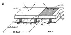
図1は、視覚ディスプレイの一連の画素中の二つの隣接画素を描いた等角投影図であり、各画素はMEMS光干渉変調器を備えている。いくつかの実施形態では、光干渉変調器ディスプレイは、これらの光干渉変調器の行/列アレイを備えている。各光干渉変調器は、互いに可変かつ制御可能な距離に位置する一対の反射層を含んでおり、少なくとも一つの可変次元をもつ共振光学キャビティを形成している。一実施形態では、一方の反射層が二つの位置の間で移動されうる。第一の位置(ここでは弛緩位置と呼ぶ)では、可動反射層は、固定部分反射層から比較的大きな距離に位置している。第二の位置(ここでは作動位置と呼ぶ)では、可動反射層は、固定部分反射層に隣接し密接して位置している。二つの層から反射する入射光は、可動反射層の位置に応じて強め合ってまたは弱め合って干渉し、各画素について全体反射状態または非反射状態のいずれかを作り出す。 FIG. 1 is an isometric view depicting two adjacent pixels in a series of pixels of a visual display, each pixel having a MEMS interferometric modulator. In some embodiments, the interferometric modulator display comprises a row / column array of these interferometric modulators. Each interferometric modulator includes a pair of reflective layers positioned at a variable and controllable distance from each other to form a resonant optical cavity having at least one variable dimension. In one embodiment, one reflective layer can be moved between two positions. In the first position (referred to herein as the relaxed position), the movable reflective layer is located at a relatively large distance from the fixed partial reflective layer. In the second position (referred to herein as the actuated position), the movable reflective layer is located adjacent to and closely in contact with the fixed partial reflective layer. Incident light reflected from the two layers interferes with each other in a constructive or destructive manner depending on the position of the movable reflective layer, creating either a total reflection state or a non-reflection state for each pixel.
図1の画素アレイの図示部分は二つの隣接する光干渉変調器12aと12bを含んでいる。左側の光干渉変調器12aでは、可動反射層14aは光学スタック16aからの所定距離の弛緩位置に図示されており、光学スタック16aは部分的反射層を含んでいる。右側の光干渉変調器12bでは、可動反射層14bは光学スタック16bに隣接する作動位置に図示されている。光学スタック16aと16b(光学スタック16と総称する)は、ここに参照するように、典型的にはいくつかの融合層を備えており、それらは、インジウムスズ酸化物(ITO)などの電極層、クロムなどの部分的反射層、透明誘電体を含みうる。したがって、光学スタック16は、電気的に伝導性で、部分的に透明で、部分的に反射的であり、たとえば透明基板20上に上記の層の一つ以上を堆積することにより作られてうる。いくつかの実施形態では、層は平行ストリップにパターニングされ、後述するようにディスプレイデバイス中の行電極を形成しうる。可動反射層14a,14bは、ポスト18の上面およびポスト18間に堆積された介在犠牲物質の上に堆積された(行電極16a,16bに直交する)一つまたは複数の堆積金属層の一連の平行ストリップとして形成してもよい。犠牲物質をエッチング除去すると、可動反射層14a,14bが光学スタック16a,16bから規定間隙19だけ離れる。アルミニウムなどの高伝導反射物質を反射層14に使用してもよく、これらのストリップがディスプレイデバイスの列電極を形成してもよい。 The depicted portion of the pixel array of FIG. 1 includes two adjacent
印加電圧がないとき、図1の画素12aに示すように、可動反射層14aと光学スタック16aの間にキャビティ19が残り、可動反射層14aは機械的弛緩状態にある。しかしながら、選択した行と列に電位差を印加すると、対応する画素の行電極と列電極の交差により形成されたコンデンサーがチャージされ、静電力が電極同士を引き寄せる。電圧が十分に高ければ、可動反射層14が変形し、光学スタック16に押し付けられる。図1の右側の画素12bに示されるように、光学スタック16内の(この図には示していない)誘電体層が短絡するのを防ぐとともに層14と層16の間の分離距離を制御しうる。その振る舞いは印加電位差の極性にかかわらず同じである。このように、反射対非反射画素状態を制御することができる行/列作動は、従来のLCDやほかのディスプレイ技術で使用される行/列作動に多くの点で類似している。 When there is no applied voltage, the
図2〜5は、表示用途の光干渉変調器のアレイを使用するための一つの代表的なプロセスとシステムを示している。 2-5 illustrate one exemplary process and system for using an array of interferometric modulators for display applications.
図2は、本発明の観点を組み込んでよい電子デバイスの一実施形態を示すシステムブロック図である。この代表的な実施形態では、電子デバイスは、ARMやPentium(登録商標)、Pentium II(登録商標)、Pentium III(登録商標)、Pentium IV(登録商標)、Pentium(登録商標) Pro、8051、MIPS(登録商標)、Power PC(登録商標)、ALPHA(登録商標)などの任意の汎用シングルまたはマルチチップマイクロプロセッサー、またはデジタルシグナルプロセッサーやマイクロコントローラー、プログラマブルゲートアレイなどの任意の専用マイクロプロセッサーであってもよいプロセッサー21を含んでいる。この分野で一般に行なわれているように、プロセッサー21は一つ以上のソフトウェアモジュールを実行するように構成されうる。オペレーティングシステムを実行することに加えて、プロセッサーは、ウェブブラウザや電話アプリケーション、電子メールプログラム、ほかのソフトウェアアプリケーションを含め、一つ以上のソフトウェアアプリケーションを実行するように構成されてもよい。 FIG. 2 is a system block diagram illustrating one embodiment of an electronic device that may incorporate aspects of the invention. In this exemplary embodiment, the electronic device is an ARM, Pentium®, Pentium II®, Pentium III®, Pentium IV®, Pentium Pro, 8051, Any general purpose single or multi-chip microprocessor such as MIPS®, Power PC®, ALPHA®, or any dedicated microprocessor such as a digital signal processor, microcontroller, programmable gate array, etc. The
一実施形態では、プロセッサー21もアレイドライバー22と通信するように構成されている。一実施形態では、アレイドライバー22は、ディスプレイアレイすなわちパネル30に信号を供給する行ドライバー回路24と列ドライバー回路26を含んでいる。図1に示したアレイの断面は図2の1−1線によって示されている。MEMS光干渉変調器については、行/列作動プロトコルは、図3に示したデバイスのヒステリシス特性を利用してよい。可動層を弛緩状態から作動状態まで変形させるにはたとえば10ボルトの電位差を必要としてよい。しかしながら、電圧がその値から低下するとき、電圧が10ボルト未満に降下する際、可動層はその状態を維持する。図3の代表的な実施形態では、電圧が2ボルト未満の降下するまで可動層は完全に弛緩しない。したがって、デバイスが弛緩または作動状態で安定している印加電圧の窓が存在する電圧の範囲(図3に示した例では約3〜7V)がある。ここでは、これを「ヒステリシス窓」または「安定窓」と呼ぶ。図3のヒステリシス特性を有するディスプレイアレイは、行ストロービングのあいだ、ストローブされた行中の作動されるべき画素が約10ボルトの電圧差にさらされ、弛緩されるべき画素が0ボルト近くの電圧差にさらされるように、行/列作動プロトコルを設計することが可能である。ストローブの後、画素は、行ストローブによっておかれた状態のままであるように、約5ボルトの定常状態電圧差にさらされる。書き込み後、各画素は、この例の3−7ボルトの「安定窓」内の電位差にある。この特徴は、図1に示した画素設計を同じ印加電圧状態の下で作動または弛緩の事前状態のいずれかに安定にする。光干渉変調器の各画素は、作動状態であれ弛緩状態であれ、実質的に固定反射層と可動反射層によって形成されるコンデンサーであるので、この安定状態は、ほとんど消費電力を伴わないヒステリシス窓内の電圧で保持することができる。印加電位が固定されていれば、実質的に電流は画素に流れ込まない。 In one embodiment, the
代表的アプリケーションでは、表示フレームは、第一行中の作動画素の所望のセットにしたがって列電極のセットをアサートすることにより作成してよい。次に行パルスを行1電極に印加し、アサートされた列線に対応する画素を作動させる。次に列電極のアサートされたセットを変更し、第二行中の作動画素の所望のセットに対応させる。次にパルスを行2電極に印加し、行2中の適当な画素をアサートされた列電極にしたがって作動させる。行1画素は行2パルスに影響されず、行1パルスのあいだに設定された状態のままである。これを一連の行の完全にわたり順次に繰り返してフレームを生成してよい。一般に、フレームは、毎秒所望のフレーム数でこのプロセスを絶えず繰り返すことにより、新しい表示データでリフレッシュおよび/またはアップデートされる。表示フレームを生成するために画素アレイの行電極と列電極を駆動するための種々さまざまなプロトコルもまた周知であり、これは本発明と共に使用してよい。 In a typical application, the display frame may be created by asserting a set of column electrodes according to the desired set of working pixels in the first row. A row pulse is then applied to the
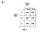
図4と5は、図2の3×3アレイに表示フレームを生成するための一つの可能な作動プロトコルを示している。図4は、図3のヒステリシス曲線を示す画素に使用してよい列と行の電圧レベルの可能なセットを示している。図4の実施形態において、画素を作動させることは、適切な列を−Vbiasに、適切な行を+ΔVにセットすることを含んでおり、それらは、それぞれ、−5ボルトと+5ボルトに一致していてもよい、画素を弛緩させることは、適切な列を+Vbiasに、適切な行を同じ+ΔVにセットして、画素を横切ってゼロボルト電位差を生成することより実施する。行電圧がゼロボルトに保持される行では、画素は、列が+Vbiasか−Vbiasかにかかわらず、それらがもとあった状態で安定している。また図4に示すように、上述したほかに逆極性の電圧を使用することができること、たとえば、画素を作動させることが適切な列を+Vbiasに、適切な行を−ΔVにセットすることを含みうることもわかるであろう。本実施形態では、画素を開放することは、適切な列を−Vbiasに、適切な行に−ΔVをセットして、画素を横切ってゼロボルト電位差を生産することにより実施する。また図4に示すように、上述したほかに逆極性の電圧を使用することができること、たとえば、画素を作動させることが適切な列を+Vbiasに、適切な行を−ΔVにセットすることを含みうることもわかるであろう。本実施形態では、画素を開放することは、適切な列を−Vbiasに、適切な行に−ΔVをセットして、画素を横切ってゼロボルト電位差を生産することにより実施する。4 and 5 illustrate one possible operating protocol for generating display frames in the 3 × 3 array of FIG. FIG. 4 shows a possible set of column and row voltage levels that may be used for the pixel showing the hysteresis curve of FIG. In the embodiment of FIG. 4, actuating the pixels includes setting the appropriate column to −Vbias and the appropriate row to + ΔV, which are set to −5 volts and +5 volts, respectively. The relaxation of the pixel, which may be done, is accomplished by setting the appropriate column to + Vbias and the appropriate row to the same + ΔV to produce a zero volt potential difference across the pixel. In rows where the row voltage is held at zero volts, the pixels are stable in their original state regardless of whether the column is + Vbias or -Vbias . Also, as shown in FIG. 4, in addition to the above, a reverse polarity voltage can be used, for example, to set the appropriate column to + Vbias and the appropriate row to −ΔV to operate the pixel. It will be understood that it can be included. In this embodiment, opening the pixel is performed by setting the appropriate column to -Vbias and -ΔV to the appropriate row to produce a zero volt potential difference across the pixel. Also, as shown in FIG. 4, in addition to the above, a reverse polarity voltage can be used, for example, to set the appropriate column to + Vbias and the appropriate row to −ΔV to operate the pixel. It will be understood that it can be included. In this embodiment, opening the pixel is performed by setting the appropriate column to -Vbias and -ΔV to the appropriate row to produce a zero volt potential difference across the pixel.
図5Bは、図5Aに示したディスプレイ配列をもたらす図2の3×3アレイに印加する一連の行と列の信号を示しているタイミング図であり、ここで作動画素は非反射である。図5Aに示したフレームを書き込む前に、画素は任意の状態であってもよく、この例では、すべての行が0ボルト、すべての列が+5ボルトにある。これらの印加電圧では、すべての画素はそれらの既存の作動状態または弛緩状態で安定している。 FIG. 5B is a timing diagram showing a series of row and column signals applied to the 3 × 3 array of FIG. 2 resulting in the display arrangement shown in FIG. 5A, where the working pixels are non-reflective. Prior to writing the frame shown in FIG. 5A, the pixels may be in any state, and in this example, all rows are at 0 volts and all columns are at +5 volts. At these applied voltages, all pixels are stable in their existing operating or relaxed state.
図5Aのフレーム中では、画素(1,1)と(1,2)、(2,2)、(3,2)、(3,3)が作動される。これを実施するため、行1の「線時間」のあいだ、列1と列2は−5ボルトにセットし、列3は+5ボルトにセットする。これは任意の画素の状態を変更しない。なぜなら、すべての画素は3〜7ボルトの安定窓にあるままであるからである。次に行1を、0から5ボルトまで上がってゼロに戻るパルスでストローブする。これは(1,1)と(1,2)画素を作動させ、(1,3)画素を弛緩させる。アレイ中のほかの画素は影響されない。行2を望むようにセットするため、列2を−5ボルトにセットし、列1と列3を+5ボルトにセットする。次に行2に印加した同じストローブは、画素(2,2)を作動させ、画素(2,1)と(2,3)を弛緩させる。再び、アレイ中のほかの画素は影響されない。列2と列3を−5ボルトに、列1を+5ボルトにセットすることにより行3を同様にセットする。行3のストローブは図5Aに示すように行3の画素をセットする。フレームを書き込んだ後、行電位はゼロになり、列電位は+5または−5ボルトの一方のままとなることが可能であり、ディスプレイは次に図5Aの配列で安定する。多数すなわち何百もの行と列に対して同じ手順を使用することが可能であることがわかるであろう。行と列の作動を実施するのに使用される電圧のタイミングとシーケンスとレベルは、上に概説した一般的な原理の範囲内で広く変えることが可能であり、上述の例は代表的なだけであり、任意の作動電圧方法もここに説明したシステムと方法で使用することが可能である。 In the frame of FIG. 5A, the pixels (1,1) and (1,2), (2,2), (3,2), (3,3) are activated. To do this, during the “line time” of
図6Aと6Bは、ディスプレイデバイス40の実施形態を示すシステムブロック図である。ディスプレイデバイス40はたとえば携帯(移動)電話とすることができる。しかしながら、ディスプレイデバイス40またはそれの少しの変形の同じコンポーネントは、テレビやポータブルメディアプレイヤーなどのさまざまなタイプのディスプレイデバイスの例ともなる。ディスプレイデバイス40は、ハウジング41とディスプレイ30とアンテナ43とスピーカー44と入力デバイス48とマイクロホン46とを含んでいる。ハウジング41は一般に、射出成形と真空成形を含む、当業者に周知なさまざまな製造プロセスのいずれかから形成される。さらに、ハウジング41は、これらに限定されないが、プラスチックや金属、ガラス、ゴム、陶器、またはそれらの組み合わせを含む、さまざまな物質のいずれかから作られうる。一実施形態では、ハウジング41は、異なる色のまたは異なるロゴや絵や記号を有しているほかの着脱部と交換されてよい(図示しない)着脱部を含んでいる。 6A and 6B are system block diagrams illustrating an embodiment of
代表的なディスプレイデバイス40のディスプレイ30は、ここに説明するように、双安定ディスプレイを含むさまざまなディスプレイのいずれかであってもよい。ほかの実施形態では、ディスプレイ30は、当業者に周知なように、プラズマやEL、OLED、STN LCD、上述したTFT LCDなどのフラットパネルディスプレイ、またはCRTやほかのチューブデバイスなどの非フラットパネルディスプレイを含んでいる。しかしながら、本実施形態を説明する目的のため、ディスプレイ30は、ここに説明するように、光干渉変調器ディスプレイを含んでいる。代表的なディスプレイデバイス40の一実施形態のコンポーネントを図6Bに概略的に示す。図示の代表的なディスプレイデバイス40はハウジング41を含んでおり、その中に少なくとも部分的に囲まれた追加コンポーネントを含むことができる。たとえば、一実施形態では、代表的なディスプレイデバイス40は、トランシーバー47に接続されるアンテナ43を含むネットワークインターフェース27を含んでいる。トランシーバー47はプロセッサー21に連結されており、それはコンディショニングハードウェア52に連結されている。コンディショニングハードウェア52は信号を整える(たとえば信号をフィルター処理する)ように構成されうる。コンディショニングハードウェア52はスピーカー45とマイクロホン46に連結されている。プロセッサー21も入力デバイス48とドライバーコントローラー29に連結されている。ドライバーコントローラー29はフレームバッファ28とアレイドライバー22に接続され、これはさらにディスプレイアレイ30に接続されている。電源50は、特定の代表的なディスプレイデバイス40設計によって必要とされるすべてのコンポーネントにパワーを供給する。 The
ネットワークインターフェース27は、代表的なディスプレイデバイス40がネットワーク上の一つ以上のデバイスと通信できるように、アンテナ43とトランシーバー47を含んでいる。一実施形態では、ネットワークインターフェース27はまたいくつかの処理容量を有し、プロセッサー21の要件を取り除いてもよい。アンテナ43は、信号の送受信用の当業者に周知の任意のアンテナである。一実施形態では、アンテナは、IEEE 802.11規格によりIEEE 802.11(a)や(b)や(g)を含むRF信号を送受信する。別の実施形態では、アンテナはBLUETOOTH(登録商標)規格によりRF信号を送受信する。携帯電話の場合、アンテナは、無線セル電話ネットワーク内で通信するために使用されるCDMAやGSM、AMPS、ほかの既知信号を受信するように設計されている。トランシーバー47はアンテナ43から受信した信号を、それらがプロセッサー21によって受信されさらに操作されうるように前処理する。トランシーバー47はまたプロセッサー21から受信した信号を、それらがアンテナ43を介して代表的なディスプレイデバイス40から送信されうるように処理する。 The
代替実施形態では、トランシーバー47はレシーバーと交換することが可能である。また別の代替実施形態では、ネットワークインターフェース27は像源と取り替えることが可能であり、像源はプロセッサー21に送る画像データを記憶または生成することができる。たとえば、像源は、画像データを収容したデジタルビデオディスク(DVD)やハードディスクドライブ、または画像データを生成するソフトウェアモジュールとすることができる。 In an alternative embodiment, the transceiver 47 can be replaced with a receiver. In yet another alternative embodiment, the
プロセッサー21は一般に、代表的なディスプレイデバイス40の動作全体を制御する。プロセッサー21は、ネットワークインターフェース27や像源からの圧縮画像データなどのデータを受信し、そのデータを行画像データに、または行画像データへ容易に処理されるフォーマットに処理する。次にプロセッサー21は処理したデータを記憶のためにドライバーコントローラー29またはフレームバッファ28へ送る。生データは、典型的には画像内の各場所における画像特性を識別する情報を指す。たとえば、そのような画像特性は、色と彩度とグレースケールレベルを含みうる。 The
一実施形態では、プロセッサー21は、マイクロコントローラーまたはCPU、論理演算装置を含み、代表的なディスプレイデバイス40の動作を制御する。コンディショニングハードウェア52は、スピーカー45に信号を送信するために、またマイクロホン46から信号を受信するために、一般に増幅器とフィルターを含んでいる。コンディショニングハードウェア52は代表的なディスプレイデバイス40内のディスクリートコンポーネントであってもよく、またはプロセッサー21やほかのコンポーネント内に組み込まれていてもよい。 In one embodiment, the
ドライバーコントローラー29は、プロセッサー21によって生成された行画像データをプロセッサー21から直接またはフレームバッファ28からとり、アレイドライバー22への高速伝送に適切な行画像データに再フォーマットする。具体的には、ドライバーコントローラー29は行画像データを、ラスター状フォーマットを有するデータ流れに再フォーマットし、それは、ディスプレイアレイ30を横切って走査するのに適した時間順序を有している。次にドライバーコントローラー29はフォーマットした情報をアレイドライバー22に送る。LCDコントローラーなどのドライバーコントローラー29はしばしばスタンドアロンの集積回路(IC)としてシステムプロセッサー21に付随されるが、そのようなコントローラーは多くの手法によって実現されてよい。それらはハードウェアとしてプロセッサー21に埋め込まれても、ソフトとしてプロセッサー21に埋め込まれても、アレイドライバー22にハードウェアに完全に集積されてもよい。 The
典型的には、アレイドライバー22はドライバーコントローラー29からフォーマットされた情報を受信し、ビデオデータを、ディスプレイのx−yマトリックスの画素から来る何百もの時には何千ものリードに毎秒何度も印加される波形の並列セットに再フォーマットする。 Typically, the
一実施形態では、ドライバーコントローラー29とアレイドライバー22とディスプレイアレイ30は、ここに説明したディスプレイのどのタイプにも適切である。たとえば、一実施形態では、ドライバーコントローラー29は、従来のディスプレイコントローラーや双安定ディスプレイコントローラー(たとえば光干渉変調器コントローラー)である。別の実施形態では、アレイドライバー22は、従来のドライバーや双安定ディスプレイドライバー(たとえば光干渉変調器ディスプレイ)である。一実施形態では、ドライバーコントローラー29はアレイドライバー22に集積されている。そのような実施形態は、携帯電話、時計、ほかの小面積ディスプレイなどの高集積システムに共通している。また別の実施形態では、ディスプレイアレイ30は、典型的なディスプレイアレイや双安定ディスプレイアレイ(たとえば光干渉変調器のアレイを含むディスプレイ)である。 In one embodiment,
入力デバイス48は、ユーザーが代表的なディスプレイデバイス40の動作を制御するのを可能にする。一実施形態では、入力デバイス48は、QWERTYキーボードや電話キーパッドなどのキーパッドや、ボタン、スイッチ、タッチセンシティブスクリーン、感圧または感熱膜を含んでいる。一実施形態では、マイクロホン46は代表的なディスプレイデバイス40用の入力デバイスである。マイクロホン46を使用してデバイスにデータを入力するとき、代表的なディスプレイデバイス40の動作を制御するためにユーザーがボイスコマンドを与えてもよい。
この分野で周知なように、電源50はさまざまなエネルギー蓄積装置を含みうる。たとえば、一実施形態では、電源50は、ニッケル−カドミウム電池やリチウムイオン電池などの充電式電池である。別の実施形態では、電源50は、再生可能エネルギー源とコンデンサー、プラスチック太陽電池と太陽電池ペイントを含む太陽電池である。別の実施形態では、電源50は壁付コンセントからパワーを受け取るように構成される。 As is well known in the art, the
いくつかの実施においては、上述したように、電子ディスプレイシステムのいくつかの場所に配置することが可能であるドライバーコントローラーに、制御プログラム化が存在する。いくつかのケースでは、制御プログラム化はアレイドライバー22に存在する。たくさんのハードウェアおよび/またはソフトウェアコンポーネントおよびさまざまな構成に対して上述した最適化が実現されてよいことは当業者であればわかるであろう。 In some implementations, as described above, there is control programming in the driver controller that can be located at several locations in the electronic display system. In some cases, control programming exists in the
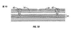
上述した原理にしたがって動作する光干渉変調器の構造の詳細は広く変更されてよい。たとえば、図7A〜7Eは、可動反射層14をその支持構造の5つの異なる実施形態を示している。図7Aは図1の実施形態の断面図であり、金属物質14のストリップが直交して延びている支持体18上に堆積されている。図7Bでは、可動反射層14がつなぎ32によってコーナーだけで支持体に取り付けられている。図7Cでは、可動反射層14が変形可能層34からつるされており、変形可能層34は可撓性金属で構成されうる。変形可能層34は、直接または間接的に、変形可能層34の周囲の周りの基板20に連結している。これらの接続はここでは支持ポストと呼ぶ。図7Dに示した実施形態は、その上に変形可能層34が横たわる支持ポストプラグ42を有している。図7A〜7Cのように、可動反射層14はキャビティの上につるされるが、変形可能層34は、変形可能層34と光学スタック16の間の穴を満たすことにより、支持ポストを形成しない。むしろ、支持ポストは平坦化物質から作られ、それは支持ポストプラグ42を形成するために使用される。図7Eに示す実施形態は、図7Dに示した実施形態に基づくが、図示しない追加の実施形態と同様に、図7A〜7Cに示した実施形態のいずれに適用してもよい。図7Eに示した実施形態では、金属またはほかの伝導物質の追加層がバス構造44を形成するために使用された。これは信号を光干渉変調器の背面に沿って転送するのを可能にし、さもなければ基板20上に形成されなければならないであろう多くの電極を取り除く。 The details of the structure of interferometric modulators that operate in accordance with the principles set forth above may vary widely. For example, FIGS. 7A-7E illustrate five different embodiments of the support structure for the movable
図7に示した実施形態では、光干渉変調器は直視型デバイスとして機能し、画像は透明基板20の正面側つまり変調器が配置される側の反対側から見られる。これらの実施形態では、変形可能層34を含め、反射層14は、基板20に対向する反射層の側にある光干渉変調器の部分を光学的に遮へいする。これは、遮へい領域が像品質に悪影響を与えずに構成され動作されることを可能にする。そのような遮へいは図7Eのバス構造44を可能にし、これは変調器の光学的特性をアドレシングとそのアドレシングに起因する動作などの変調器の電気機械の特性から分離する能力を提供する。この分離可能な変調器アーキテクチャは、変調器の電気機械的観点と光学的観点のために使用される構造設計と物質が互い独立に選択され機能することを可能にする。さらに、図7C〜7Eに示した実施形態は、反射層14の光学的特性の機械的特性からの減結合を得るという追加の利点を有し、それは変形可能層34によって実現される。これは、反射層14に使用する構造設計と物質を光学的特性に対して最適化し、また変形可能層34に使用する構造設計と物質を所望の機械的特性に対して最適化すること可能にする。 In the embodiment shown in FIG. 7, the interferometric modulator functions as a direct view device, and the image is viewed from the front side of the
変形可能層34の可能な構成を図8aと8bに示す。これらは、変調器の背面から見た図であり、図1に示した変調器の底と見なしてよい。図8Aでは、変形可能層34は、その角が支持ポスト72a〜dに支持された可撓性膜の形をとっている。支持ポスト72a〜dは基板20および/または光学スタック16などの基板20上の層に固定されている。図7Dと7Eに示した実施形態では、支持ポスト72a〜dは支持ポストプラグ42の形をとっている。変形可能層34は、大きい中央背面支持体74と四つの小さい周辺支持体76a〜dとを介して、下に横たわる反射層14に連結されている。反射層14はその境界が破線によって定められている。背面支持体74と周辺支持体76a〜dは、支持ポストプラグ42と同じ平坦化物質、または任意の適切な物質で構成することができる。変形可能層34は、光学スタック16の上に反射層14をつるす。 A possible configuration of the
あるいは、図8Bでは、変形可能層34はパターニングされ、各支持ポスト72a〜dに連結された薄い線形のストラップ78a〜dを形成している。ストラップは中央支持体74のそばで反射層14に取り付けられている。図8Aと8Bの構成は多くの可能性のうちの二つの選択肢である。本発明に有用な光干渉変調器は、反射層14に所望の動作の自由度およびその動作の所望の機械的特性を与える任意の構成を備えていてもよい。反射層14の機械的および光学的特性を分離することにより与えられる自由度に加えて、変形可能層34により反射層14をつるすことは、追加の挑戦を示すことが可能である。たとえば、つるされた反射層14は、光干渉変調器の光学的特性に影響する動作および/または変形をこうむるかもしれない。そのような動作は、光干渉変調器を組み込んだディスプレイの品質を低下させるかもしれない。たとえば、反射層14は、反射層14が非拘束すなわち静止位置にあるとき、傾斜および/または丸まりをこうむるかもしれない。さらに、反射層14が静止位置にあるとき反射層14は側方および/または回転の方向への不所望な動作をこうむるかもしれない。多くの実施形態では、反射層14は、作動位置において、光学スタック16に、または直接または間接的に光学スタック16の上にある層に接する。これらの実施形態では、反射層14の傾斜および/または丸まりは、一般に静止位置ほど頻繁に起こらないだろう。しかしながら、反射層14は、作動位置にあるときに、側方動作および/または回転動作など、不所望な動作をまだこうむるかもしれない。さらに、反射層14は、静止位置と作動位置の間の位置にあるときに、不所望な動作および/または変形をこうむるかもしれない。 Alternatively, in FIG. 8B, the
これを改善するため、図9と10に示すように、一つ以上の部材90を光干渉変調器の構造に組み込んで、所望の光学的出力を許す位置および/または形態に反射層14を維持してよい。これらの一つ以上の部材はここでは「反傾斜部材90」と呼ぶ。反傾斜部材90は、反射層14を安定させるおよび/または反射層14の動作範囲を制約する静止橋台または接触点を反射層14に提供することにより、反射層14の不所望な動作および/または変形を抑制する。たとえば、いくつかの実施形態では、反射層14が静止位置にあるときに、橋台は、反射層14の上面(すなわち基板20から遠い対向している反射層14の表面)に接触する。このように、反傾斜部材90は、反射層14が静止位置にあるときに基板20から遠ざかる反射層14の動作を抑制したり、反射層14が静止位置にあるときに光学スタック16に実質的に平行な配置状態に反射層14を維持したりすることが可能である。ほかの実施形態では、反傾斜部材90は、反射層14が静止位置にあるときに、光学スタック16に対して一定角度(すなわち非平行配置状態)に反射層14を維持して、静止状態の所望の光学反応を作り出す。 To improve this, as shown in FIGS. 9 and 10, one or
好都合に、反射層14が静止位置にあるときの反傾斜部材90と反射層14との接触は、反射層14を実質的な平面配置状態に維持し、したがって反射層14の丸まりおよび/またはほかの不所望な変形を抑制する。いくつかの実施形態では、反傾斜部材90は、反射層14が静止位置にあるときに反射層14を実質的な平面配置状態に維持する反傾斜部材90の能力を高めるために、反射層14が静止位置にあるときに反傾斜部材90に接触する反射層14の面積の割合を最大限にするように設計されている。本発明の光干渉変調器に利用される反傾斜部材90の数および/または構成もまた、反射層14を実質的な平面配置状態に維持することを支援するように設計されてよい。 Conveniently, contact between the
いくつかの実施形態では、反傾斜部材90は、一つ以上の反傾斜部材90によって定められた経路の外側に反射層14が移動する際に反射層14に接触することにより反射層14の動作範囲を定める一つ以上の一定位置を占めてよい。たとえば、反射層14の周囲に沿って位置した反傾斜部材90は、光学スタック16に実質的に平行な方向および/または回転方向の反射層14の動作を抑制してよい。 In some embodiments, the
反傾斜部材は一般にどのような物質で構成されてもよく、またどのような位置および/または所望の構造的機能を果たしうる構成を占めてもよい。反傾斜部材のいくつかの実施形態をより完全に以下に説明する。 The anti-tilt member may generally be composed of any material and may occupy any position and / or configuration capable of performing the desired structural function. Several embodiments of anti-tilt members are described more fully below.
図9は、図7C〜7Eに示したような3×3アレイの光干渉変調器の背面(すなわち基板20と向かい合う側)の平面図であり、光干渉変調器はディスプレイ中の画素80を備えている。図示の実施形態では、各光干渉変調器は四つの反傾斜部材(たとえば90(a),90(b),90(c),90(d))を含んでおり、一つの反傾斜部材90は各光干渉変調器の各辺を実質的に二分している。しかしながら、反傾斜部材の個数および/または配置はどのようなものを使用してもよい。反傾斜部材90(b)と90(c)など、隣接する光干渉変調器の間に位置する反傾斜部材90は、それらの光干渉変調器に共有される。反傾斜部材90(a)と90(d)など、画素80の周囲に位置する反傾斜部材は、画素80内のただ一つの光干渉変調器に利用される。しかしながら、画素80内の光干渉変調器の位置は、反傾斜部材90の配置を要求する必要はない。たとえば、追加の反傾斜部材90を組み込んで特定の用途に合わせることが可能である。先に説明したように、反傾斜部材90は、光学スタック16に対してある高さ(間隙)を超える基板に実質的に垂直な方向の動作など、反射層14の不所望な動作および/または変形を防止することができる。 FIG. 9 is a plan view of the back surface (ie, the side facing the substrate 20) of the 3 × 3 array of interferometric modulators as shown in FIGS. 7C-7E, which includes the
図9に示した光干渉変調器のおのおのには四つの反傾斜部材90が付随しているが、いくつかの反傾斜部材90を使用しても、丸まりと傾斜など、反射層14の不所望な動作を抑制する所望の利益を提供することができる。たとえば、二つの反傾斜部材90を(図示しない)光干渉変調器の四つの辺(対辺または隣辺)のうちの二つに配置することができる。別の(図示しない)実施形態では、反傾斜部材90は、光干渉変調器の角に、たとえば支持ポスト42(説明の都合上、追加のバス構造44は図示していない)から延びて配置する。好ましくは、光干渉変調器の周囲の周りの反傾斜部材90の位置は、角ポスト42または変形可能機械的層34と干渉しないように選択する。 Each of the interferometric modulators shown in FIG. 9 is accompanied by four
さらに、反傾斜部材90の個数は画素80のサブ画素すなわち副構成要素について異ならせることが可能であり、それは、たとえば、副構成要素の色、および/または、キャビティの深さ、ディスプレイの外周への副構成要素の近接度、副構成要素の物質特性に基づく。キャビティをさらに横切って延びている反射層14(たとえば赤色光を反射するそれら)またはディスプレイの周囲に位置する反射層14は共に、より浅い光学キャビティに関連するかディスプレイの内部に位置する反射層14よりも丸まりおよび/または傾斜により弱いかもしれない。さらに、ディスプレイ中の各画素80は、異なる個数の反傾斜部材90を含むことができる。追加の反傾斜部材90は、より大きな安定性のために比較的大きな光干渉変調器を固定するのに使用することができる。 Furthermore, the number of
図9には反傾斜部材90はほぼ矩形形状であるとして示している。しかしながら、以下により詳細に説明するように、反傾斜部材はさまざまな形状であってもよい。たとえば、反射層14に重なる反傾斜部材90の部分の形状および/または大きさは、反射層14の不所望な動作および/または変形を防止する反傾斜部材90の能力を高めるように設計されてよい。 In FIG. 9, the
反傾斜部材90は反射層14の背後に配置されており、このため反射層14により得られる光学遮へいのために人間の目には本質的に見えないことを図9において理解することができる。したがって、反傾斜部材は、このような光干渉変調器を組み込んだ光干渉変調器やディスプレイデバイスの光学性能に影響することなく反射層14全体の動作に影響するようにキャビティの背面を横切って配分することができる。説明の都合上、変形可能層34は図9に示していない。光干渉変調器の後ろの変形可能層34の可能な構成の例は、先の図8Aと8Bに示される。 It can be seen in FIG. 9 that the
図10は、反傾斜部材90のいくつかの実施形態の概略図である。図10aと10bは、おのおのが二つの隣接する光干渉変調器に関して機能する、図9中の90(b)と90(c)などの反傾斜部材の断面図の概略図である。図10cと10dは、おのおのがただ一つの隣接する光干渉変調器に関して機能する、図9中の90(a)と90(d)などの反傾斜部材の概略図である。反傾斜部材90は、ポストやシャンク、シャフト、ほかの構造体94を有し、これは、ここでは「シャフト部」94と呼び、シャフト部94の端部に取り付けられたヘッド部92とともに基板20に対して実質的に直立姿勢に配置される。シャフト部94の末端部98は、光学スタック16に、あるいは直接または間接的に光学スタック16の上または下にある別の静止層(たとえば基板20)に取り付けられる。シャフト部94の末端部98または反傾斜部材90のほかの部位が、反傾斜部材90に適切な支持を提供することが可能などのような別の構造体に付けられてもよい。ヘッド部92は、末端部98の反対側のシャフト部94の端部に取り付けられている。ヘッド部の構造と機能について以下にさらに詳細に説明する。シャフト部94は、角ポスト42に使用される物質と同じでありうる物質、またはほかの適切な物質で構成されてもよい。シャフト部94は、その構造的機能を果たすに十分な高さと幅と形状を有している。特定のシャフト部94の幅は、シャフト部94用に選んだ物質に依存してよい。多くの適用では、シャフト部94は、約0.1ミクロンと10ミクロンとの間の幅、特には約3ミクロンの幅を有している。以下により完全に説明するように、シャフト部94の高さは、光干渉変調器中の反射層14と光学スタック16の間の間隙の高さに依存してよい。いくつかの適用では、シャフト部は約1ミクロンないし約10ミクロンの高さを有している。図示した実施形態では、シャフト部94は若干円錐形状をしている。シャフト部94は、図示した実施形態で示した円錐形状に加えて、特定用途に適した丸形や長方形、正方形、三角形、その他など、どのようなさまざまな長い形状に形成されてもよいことが予想される。どのような形状も使用することが可能であるが、丸形は反傾斜部材90の製造を簡単にして好適でありうる。 FIG. 10 is a schematic view of some embodiments of the
上述したように、図10に示した反傾斜部材は、反射層が静止位置にあるときに反射層14に接触するヘッド部92を備えている。ヘッド部92は、後述する一つ以上のエレメント、またはその構造的機能を果たしうるどのような構造体を備えてよい。 As described above, the anti-tilt member shown in FIG. 10 includes the
ヘッド部92が備えうるエレメントの一つは、シャフト部94から延びた突部である。図10に示すように、突部は、光学スタック16から遠いシャフト部94の端部に位置する拡大チップまたはほかの構造体を備えていてよい。さまざまな実施形態では、ヘッド部92の幅の少なくとも一部がシャフト部94の幅より大きく、シャフト部94の幅のたとえば約2〜4倍以上の幅を有している。いくつかの実施形態では、ヘッド部の形状と大きさは、反射層14が静止位置にあるときに、ヘッド部92と反射層14の間の接触の表面積を最大にして、反射層14を平面配置状態に維持するのを助けるように設計されている。ヘッド部92は、図10a〜10cに示すように、シャフト部94に実質的に垂直に、またはシャフト部94に鋭角に、またはシャフト部94に対して反傾斜部材が意図した機能を果たしうるどのような方向に配置されてもよい。ヘッド部92は、ヘッド部92がその構造的機能を果たしうる任意の距離だけシャフト部94から延びていてもよい。好都合に、ヘッド部92は、反射層14が静止位置において反傾斜部材90に接しているときに反傾斜部材90が反射層14を平面配置状態に維持するに十分な距離だけシャフト部94から延びている。 One of the elements that the
ヘッド部92は、さまざまなほかの形状、たとえば、中実または中空の円錐形や、やじり、かえし、球形、キノコ頭、ほかのタイプの突出構造をとりうることが理解されよう。いくつかの実施形態では、シャフト部94とヘッド部92は、図10dに示すように、ステッキまたはフックの形状、または反射層14の上面の上に延びている湾曲部を有するほかの構造をしている。ステッキ形状は、支持ポスト42と反傾斜部材90を同一処理ステップの間に機械加工するのを可能にして有利でありうる。ヘッド部92の比較的鈍い端部は、光干渉変調器の変形可能層34および/または背面バス44、ほかの構造部材と、引っかかったり干渉したりしないことが好ましい。いくつかの実施形態では、反射層14と相互作用する反傾斜部材90の部分が、相互作用の安定性やほかの性質を促進するために修正される。たとえば、ヘッドの下側96は、反射層14が静止位置にあるときに反射層14の上面に接触して反射層14の丸まりおよび/または傾斜、ほかの不所望な動作を抑制する橋台を備えていてよい。 It will be appreciated that the
図10からわかるように、下側96は一般に平面である。しかしながら、下側96は、反射層14との接触を促進するために、凹状に湾曲させて反射層14の一部が収まりうる(図示しない)くぼみを形成するように修正してよい。下側96はまた、凸状に湾曲させて、(図示しない)反射層14のくぼみ部と相互作用する突部を形成してもよい。下側96はまた、反射層14の安定化を支援するため、粗く処理した面または隆起部や(図示しない)ほかの引っかかりデバイスを付随させた面を有していてもよい。しかしながら、下側96はまた、製造コスト低減のために、滑らかであってもよい。 As can be seen from FIG. 10, the
ヘッド部92はまた、図10dに示すように、フックであってもよい。フックは、シャフト94から外側に延びている放射部を有していてよい。好都合に、フックは、シャフト94から遠く(図示しない)放射部の末端に向かって位置する湾曲部を有することも可能である。湾曲部は、(図示しない)反射層14の側方安定性を提供するように反射層14の上面のくぼみまたはレセプタクルを受ける大きさおよび構成とすることが可能である。くぼみかレセプタクルは、反射層14のいくつかの実施形態の追加特徴である。望ましくは、湾曲部は遠位の円周に沿った面取り面またはテーパーを有し、湾曲部が反射層14の上面中のくぼみに容易にはまるのを可能にする。湾曲部のないフックの実施形態においては、放射部が反射層14の上面に接触してよい。 The
シャフト部94とヘッド部92は、光学スタック16の面上に、あるいは直接または間接的に光学スタック16の上または下にあるほかの静止層の面上に形成した(図示しない)クリップの形をとることも可能である。さまざまな実施形態では、クリップは、反射層14の外周部の周りにはまり、反射層14がキャビティ内に移るのを可能にする大きさおよび形状となっている。クリップは、その目的を達成するさまざまな手法で構成することが可能である。たとえば、一実施形態では、クリップは実質的にC字状をしていて、クリップの凹部がその中に反射層14を捕らえる部分を形成している。一実施形態では、C字状のクリップの下部は光学スタック16に取り付けられ載っている。あるいは、間隔を置いて背中合わせに接近させた一対の半硬質の逆L字状の部材は、二つの隣接する光干渉変調器の反射層14の不所望な動作および/または変形を抑制する。当業者であればわかるように、単一L字状や単一T字状のクリップなど、さまざまなほかのクリップ形状を反傾斜部材の目的を達成するために使用することが可能である。 The
図10bは、段差付き上面を有するほぼ矩形形状をしたヘッド部92を示している。矩形ヘッド部92の各端部は異なる光干渉変調器に向かって延びている。段差付き上面は、反射層14が静止位置にあるときの反射層14と光学スタック16の間の距離の違いによる隣接する光干渉変調器のキャビティの深さの違いに相当している。たとえば、図10bを参照すると、反傾斜部材90の左側に合体する光干渉変調器は、反傾斜部材の右側に合体する隣の光干渉変調器のキャビティより浅いキャビティを有している。ほかの実施形態において、平坦ヘッドや多段ヘッド、任意の適切な形状のヘッドもまた使用することが可能である。たとえば、隣接する二つの光干渉変調器のキャビティ深さが同じ実施形態では、図10aに示すように、ヘッド部92は段差がなくてよい。あるいは、図9の反傾斜部材90(a)と90(c)のように、反傾斜部材90がただ一つの光干渉変調器に対して機能する場合には、図10cと10dに示すように、シャフト部94には単一ヘッド部92だけが取り付けられている。さまざまな実施形態では、ヘッド部92の厚さはヘッド部92の物質特性に依存して変更することができる。 FIG. 10b shows a substantially
図11を参照すると、図9に示した11−11線に沿ったアレイの断面図を示している。反傾斜部材90は、光学スタック16から、あるいは直接または間接的に光学スタック16の上または下にある別の静止層(たとえば基板20)から真上に延びている。シャフト部94は、反射層14を安定させるために相互作用する特定の光干渉変調器および特定用途に応じて、さまざまな長さおよび間隔とすることができる。光干渉変調器の両側に位置するシャフト部94は、側方に少なくとも、安定させる反射層14を収容するに十分な幅の間隔を置いて配置されている。望ましくは、シャフト部94は、反射層14のクリアランスを提供するために、反射層14の側辺間の距離よりもわずかに大きい距離だけ離して間隔を置いて配置されている。多くの適用では、シャフト部94の間の距離は、約10ミクロンと約200ミクロンの間に、特に約100ミクロンである。 Referring to FIG. 11, a cross-sectional view of the array along the line 11-11 shown in FIG. 9 is shown. The
図11に示した三つの光干渉変調器は静止状態にある。図示したように、左端の光干渉変調器は浅い光学キャビティを有している(すなわち反射層14が静止位置にあるときの反射層14と光学スタック16の間の距離が短い)。異なるキャビティ寸法を収容するため、左端と中央の光干渉変調器間に位置する反傾斜部材90は段差付きヘッド部92を有し、ヘッド部92の左側は左端の光干渉変調器の反射層14の上面に接触し、ヘッド部92の右側は中央の光干渉変調器の反射層14の上面に接触している。段差付きヘッド部は、ヘッド部92の遠位面が変形可能層34に干渉する機会を減らし、製造を簡単にする。この目的のため、ヘッド部92の端部の厚さは、反射層14の上面と変形可能層34の底面の間に適合するように有利に選択される。 The three interferometric modulators shown in FIG. 11 are in a stationary state. As shown, the leftmost interferometric modulator has a shallow optical cavity (ie, a short distance between the
好都合に、シャフト部94とヘッド部92のおのおのは、基板20に実質的に平行な、基板20に実質的に垂直な方向および/または回転方向への反射層14の少なくとも一部の動作を抑制する。いくつかの実施形態では、反射層14の左右や側方や回転の動作は、シャフト部94と一つ以上の反傾斜部材90との接触によって抑制され、反傾斜部材90は、光干渉変調器の光学スタック16またはほかの構造体に固定されており、横断や側方や回転の方向の反射層14の動作に対する停止体として働くのに十分に硬質である。横断や側方や回転の方向の反射層14の動作の抑制は有利である。なぜなら、そのような動作は光学的ひずみに形を変え、ディスプレイの清澄度に強い影響を与えうるからである。この動作はまた、次に、反射層14をヘッド92の下から回転させたりスリップさせたりしうる。 Advantageously, each of the
いくつかの実施形態では、変形可能層34は、反射層14とその下の静止層(光学スタック16を含む)との間にあらゆる電気的な力がないとき、反射層14に復元力を与える。好都合に、復元力は、反射層14が静止位置にあるときに反射層14を引き上げて反傾斜部材90に接触させるのに十分である。好ましくは、反射層14の動作の範囲が動作電圧まで印加されるまで最小となる復元力が選択される。好都合に、復元力を選択することによって、電圧と色が独立に制御されるように光干渉変調器を最適化することができる。 In some embodiments, the
図12は、図9に示した12−12線に沿ったアレイの断面図であり、各光干渉変調器の角に位置する支持ポスト42とバス構造44を示している。反傾斜部材は、各光干渉変調器の反射層14の辺を二分している(12−12視は反射層14の角に対する対角線に沿った断面を示している)ので、図11では見えない。この構成は、反傾斜部材90が支持ポスト42および/またはバス構造44の機能性に干渉しないように好適でありうる。しかしながら、反傾斜部材は、光干渉変調器の角を含め、支持ポスト42とバス構造44に対して任意の位置に配置することができる。 FIG. 12 is a cross-sectional view of the array along line 12-12 shown in FIG. 9, showing
さまざまなタイプの干渉計測デバイスの製造は、たとえば、米国特許出願公開2004/0051929号を含め、さまざまな公開文献に説明されている。一連の物質堆積とパターニングとエッチングのステップを含め、この技術分野に周知な種々さまざまな技術を使用して上述の構造体を製造してよい。たとえば、反傾斜部材90は、光干渉変調器のほかの層に使用してよい堆積とリソグラフィーの技術を使用する共通の薄膜プロセス互換物質から作ることができる。反傾斜部材90の物質は角ポストに使用する物質と同一とすることができる。あるいは、異なる物質を使用することも可能である。反傾斜部材90を製造する代表的な過程について図13を参照しながら説明する。 The production of various types of interferometric devices is described in various published documents, including, for example, US Patent Application Publication No. 2004/0051929. A variety of techniques well known in the art may be used to fabricate the structure described above, including a series of material deposition, patterning and etching steps. For example, the
図13は、図11に類似する断面図であり、反傾斜部材90を有する光干渉変調器の製造に適用される物質層をさらに示している。 FIG. 13 is a cross-sectional view similar to FIG. 11, and further illustrates a material layer applied to the manufacture of an interferometric modulator having an
異なる構成を有するここに説明する実施形態は、反傾斜部材90の形成に共通するいくつかの処理ステップを有していてよい。光干渉変調器は透明基板20上に典型的に構築されている。光学スタック16は基板20上に堆積され、典型的には、インジウムスズ酸化物(ITO)などの適切な物質からの基板上に形成された(図示しない)電極層、クロムなどの(図示しない)部分的反射層、(図示しない)誘電体を含め、いくつかの融合層を備えている。透明基板の視野面は、基板の「底面」であり、光学スタック16が形成される側の基板の反対側である。ここに示さないプロセスでは、電極と金属層は、パターニングされエッチングされ、電極列や電極行、ディスプレイ設計に必要なほかの有用な形状を形成する。 Embodiments described herein having different configurations may have several processing steps common to the formation of the
光学スタック16の上に第一の犠牲層130(a)と反射層14を形成する。犠牲層130は、その上に反射層14がつるされるキャビティの寸法を決定する。上に論じたように、色変調器は、結果の画像中の各画素に対して三つの変調器素子を使用することによって形成してもよい。光干渉変調器では、キャビティの寸法は、しばしば干渉の性質を決定する。色ピクセルを形成する一つの方法は、三つの異なる深さのキャビティからの結果の静止色が赤と緑と青となるようにキャビティを異なる深さに作ることである。キャビティの干渉特性はそれらの深さに直接影響される。これらのキャビティ寸法の変化を作り出すため、一つまたは二つまたは三つの犠牲層130(a),130(b),130(c)をそれぞれ堆積してよい。第一の層130(a)を堆積し、マスクし、パターニングして各画素を形成する三つの変調器の一つの領域を定め、次に第二の層130(b)を堆積する。次に、この層に第二のマスクを塗布し、パターニングして各画素を形成する第二の変調器とともに上で定めた第一の変調器の結合領域を定める。最後に、第三の犠牲層130(c)を塗布する。第三の層130(c)は、その厚さが各画素を形成する変調器の三つすべてに含まれるので、パターニングする必要はない。 A first sacrificial layer 130 (a) and a
ここに説明した三つの独立の堆積層130(a)〜130(c)は必ずしも同じ厚さではないだろう。したがって、変調器はさまざまな層の合同厚さに相当するキャビティ高さの範囲を有することができる。たとえば、画素内の隣接する光干渉変調器は、三つ層の合同厚さ、および/または、二層の合同厚さ、単一犠牲層の合同厚さに相当するキャビティ高さを有してよい。犠牲層物質を除去するとき、キャビティ寸法は、三つの犠牲層のさまざまな合同層にしたがって変化し、たとえば、赤と緑と青などの三つの異なる色に相当するキャビティ寸法の変化をもたらす。 The three independent deposited layers 130 (a) -130 (c) described herein will not necessarily be the same thickness. Thus, the modulator can have a cavity height range corresponding to the combined thickness of the various layers. For example, adjacent interferometric modulators in a pixel may have a cavity height corresponding to the combined thickness of three layers and / or the combined thickness of two layers, the combined thickness of a single sacrificial layer. Good. When removing the sacrificial layer material, the cavity dimensions change according to the various congruent layers of the three sacrificial layers, resulting in changes in the cavity dimensions corresponding to, for example, three different colors such as red, green and blue.
反傾斜部材90を形成するため、反射層14の上にフォトレジスト層を堆積し適切にパターニングする。反射層14をパターニングした後、第四の犠牲層130(d)を追加する。次に、反傾斜部材90のための穴を、犠牲層130を通って光学スタック16までドリルであける。円形ドリルを使用する実施形態では、結果のシャフトは望ましいことに丸形を有する。次に、ポスト物質を追加し、反射層14の外周から張り出すようにパターニングする。 In order to form the
選択した変調器に応じて、追加の処理ステップは、角ポスト42(図12を参照)、変形可能層34などを形成することができる。これらの追加のステップは前のステップと組み合わせることが可能である。たとえば、角ポストの高さまで延びている曲がったまたはステッキ形状の反傾斜部材90は、ポストの機械加工と同時に機械加工することが可能である。最後に、バス層を使用しないならば、犠牲層130(a)と130(b)と130(c)と130(d)を除去する。結果の変調器は、その中に反射層14が光学スタック16の上につるされたキャビティを有する。腐食作用作業はまた反傾斜部材90を形成する。反射層14が(図示しない)反傾斜部材90のヘッド部に接触するとき、光学スタック16から立ち去る反射層14の自然な傾向を利用することが可能である。 Depending on the modulator selected, additional processing steps can form corner posts 42 (see FIG. 12),
反射層14の下と上から犠牲層を除去する際、犠牲層130(a)と130(b)と130(c)を除去する前に、犠牲層130(d)を除去してよい。犠牲層130(d)を除去した状態では、反射層14を引っ張る犠牲層130(c)のために、犠牲層130(c)が反射層14を非分布荷重にさらすかもしれない。反傾斜部材90なしでは、この非分布荷重は、反射層14の面の丸まりなど、反射層14の不所望な動作を招く可能性がある。好都合に、犠牲層130の除去の間、反傾斜部材90が反射層14の不所望な動作を抑制することができる。 When removing the sacrificial layer from below and above the
(図示しない)代替アプローチでは、物質層の異なる配置を使用して、反傾斜部材90を有する光干渉変調器を製造する。このアプローチでは、犠牲層130(a)と130(b)と130(c)の堆積は全面的な堆積であり、色画素分離は反傾斜部材90の高さのパターニングによって得られる。この設計は、所望の最低の間隙から最高の間隙まで幅広く、反射層14への十分な押上げ力を必要とする。この設計は、異なる色の画素間に段差の高さ差がないので、最終の平坦化ステップにとって顕著な利点を有している。 In an alternative approach (not shown), a different arrangement of material layers is used to produce an interferometric modulator having an
この手法では、光干渉変調器の製造と動作が改善されてよい。反射層14の(傾斜や丸まりなどの)不所望な動作を抑制することは表示品質を改善する。電気機械特性から光学的特性を分離することは、変調器の光学的特性から変形可能層34を分離するため、事前に利用不可能な好機をもたらしてよい。 This approach may improve the manufacture and operation of the interferometric modulator. Suppressing undesired movement (such as tilting or rounding) of the
上記の詳細な説明はさまざまな実施形態に適用した新規な特徴を図示し説明し指摘したが、ここに示したデバイスやプロセスの形態と詳細は実施形態の要旨から逸脱することなくさまざまな省略と置換と変更が当業者によってなしうることが理解されよう。光干渉変調器の上述した特徴を組み込む方法は、この分野において通常の知識を有するものには容易に明白であろう。さらに、これらの特徴の一つ以上は、光干渉変調器のほかの構成はもちろん、どのような実施形態に適用してよい。わかるように、ここに述べた特徴と利点のすべてを含んでいるとは限らない反傾斜部材を提供してもよく、いくつかの特徴をほかから分けて使用し実施してもよい。 Although the foregoing detailed description has illustrated and described novel features applied to various embodiments, the forms and details of the devices and processes shown herein may be omitted and described without departing from the spirit of the embodiments. It will be appreciated that substitutions and modifications can be made by those skilled in the art. Methods that incorporate the above-described features of interferometric modulators will be readily apparent to those having ordinary skill in the art. Furthermore, one or more of these features may be applied to any embodiment as well as other configurations of interferometric modulators. As can be appreciated, an anti-tilt member may not be provided that includes all of the features and advantages described herein, and some features may be used and implemented separately.
Claims (50)
Translated fromJapanese前記基板の上に位置し、入射光に対し少なくとも部分的に透過性のある光学層と、
前記基板の上に位置し、前記光学層から第一の距離だけ離れた第一の位置と前記光学層から第二の距離だけ離れた第二の位置との間で移動可能なミラーであって、第一の距離は第二の距離よりも大きく、前記基板から離れた表面を有するミラーと、
前記ミラーが第一の位置にあるときに前記ミラーの前記表面に接触する少なくとも一つの静止部材とを備え、前記少なくとも一つの静止部材は、前記ミラーが第一の位置にあるときに前記ミラーの少なくとも一部の動作を抑制するように構成されている、光干渉変調器。A substrate,
An optical layer located on the substrate and at least partially transparent to incident light;
A mirror located on the substrate and movable between a first position separated from the optical layer by a first distance and a second position separated from the optical layer by a second distance; The first distance is greater than the second distance and having a surface remote from the substrate;
At least one stationary member that contacts the surface of the mirror when the mirror is in a first position, wherein the at least one stationary member is the mirror when the mirror is in the first position. An interferometric modulator configured to suppress at least some operation.
基板と、
前記基板の上に位置し、入射光に対し少なくとも部分的に透過性のある光学層と、
前記基板の上に位置し、前記光学層から第一の距離だけ離れた第一の位置と前記光学層から第二の距離だけ離れた第二の位置との間で移動可能なミラーであって、第一の距離は第二の距離よりも大きく、前記基板から離れた表面を有するミラーと、
前記ミラーが第一の位置にあるときに前記ミラーの前記表面に接触する少なくとも一つの静止部材とを備え、前記少なくとも一つの静止部材は、前記ミラーが第一の位置にあるときに前記ミラーの少なくとも一部の動作を抑制するように構成されている、視覚ディスプレイデバイス。A visual display device comprising a plurality of interferometric modulators, each interferometric modulator being
A substrate,
An optical layer located on the substrate and at least partially transparent to incident light;
A mirror located on the substrate and movable between a first position separated from the optical layer by a first distance and a second position separated from the optical layer by a second distance; The first distance is greater than the second distance and having a surface remote from the substrate;
At least one stationary member that contacts the surface of the mirror when the mirror is in a first position, wherein the at least one stationary member is the mirror when the mirror is in the first position. A visual display device configured to inhibit at least some movement.
前記プロセッサーと電気的通信状態にあるメモリーデバイスとをさらに備えている請求項27の視覚ディスプレイデバイス。A processor configured to process image data in electrical communication with the plurality of interferometric modulators;
28. The visual display device of claim 27, further comprising a memory device in electrical communication with the processor.
前記第一のコントローラーに前記画像データの少なくとも一部を送るように構成された第二のコントローラーとをさらに備えている請求項28の視覚ディスプレイデバイス。A first controller configured to send at least one signal to the plurality of interferometric modulators;
30. The visual display device of claim 28, further comprising a second controller configured to send at least a portion of the image data to the first controller.
入射光を少なくとも部分的に透過するための手段と、
光を反射するための手段と、
前記反射手段を安定化させるための手段とを備えており、
前記少なくとも部分的透過手段は前記支持手段の上に位置し、
前記反射手段は、前記支持手段の上に位置していて、前記少なくとも部分的透過手段から第一の距離だけ離れた第一の位置と前記少なくとも部分的透過手段から第二の距離だけ離れた第二の位置との間で移動可能であり、第一の距離は第二の距離よりも大きく、前記反射手段は前記支持手段から離れた表面を有しており、
前記安定化手段は、静止していて、前記反射手段が第一の位置にあるときに前記反射手段を所望の配置状態に維持するように構成されており、前記安定化手段は、前記反射手段が第一の位置にあるときに前記反射手段の前記表面に接触する、デバイス。Means for supporting the interferometric modulator;
Means for at least partially transmitting incident light;
Means for reflecting light;
Means for stabilizing the reflecting means,
The at least partial transmission means is located on the support means;
The reflecting means is located on the support means and has a first position separated from the at least partially transmissive means by a first distance and a second distance from the at least partially transmissive means. The first distance is greater than the second distance, the reflecting means has a surface remote from the support means;
The stabilizing means is stationary and is configured to maintain the reflecting means in a desired arrangement when the reflecting means is in a first position, the stabilizing means comprising the reflecting means Wherein the device contacts the surface of the reflecting means when in a first position.
基板と、
前記基板の上に位置し、入射光に対し少なくとも部分的に透過性のある光学層と、
前記基板の上に位置し、前記基板から離れた表面を有する可動ミラーと、
静止部材とを備えている
光干渉変調器を用意し、
前記光学層から第一の距離だけ離れた第一の位置と前記光学層から第二の距離だけ離れた第二の位置との間で前記ミラーを移動させ、第一の距離は第二の距離よりも大きく、
前記ミラーが第一の位置にあるときに前記ミラーの前記表面を前記静止部材に接触させ、これにより前記ミラーが第一の位置にあるときに前記ミラーの少なくとも一部の動作を抑制する、方法。A method of reducing the movement of a mirror in an interferometric modulator,
A substrate,
An optical layer located on the substrate and at least partially transparent to incident light;
A movable mirror located on the substrate and having a surface remote from the substrate;
An interferometric modulator provided with a stationary member,
Moving the mirror between a first position separated from the optical layer by a first distance and a second position separated from the optical layer by a second distance, wherein the first distance is a second distance; Bigger than
Contacting the surface of the mirror with the stationary member when the mirror is in a first position, thereby inhibiting movement of at least a portion of the mirror when the mirror is in the first position .
基板を設け、
前記基板の上に位置し、入射光に対し少なくとも部分的に透過性のある光学層を設け、
前記基板の上に位置し、前記基板から離れた表面を有し、前記光学層から第一の距離だけ離れた第一の位置と前記光学層から第二の距離だけ離れた第二の位置との間で移動可能な可動ミラーを設け、第一の距離は第二の距離よりも大きく、
前記ミラーが第一の位置にあるときに前記ミラーの前記表面に接触し、前記ミラーが第一の位置にあるときに前記ミラーの少なくとも一部の動作を抑制するように構成された静止部材を設ける、方法。A method of forming an interferometric modulator,
Provide a substrate,
An optical layer located on the substrate and at least partially transparent to incident light;
A first position located on the substrate and having a surface remote from the substrate, separated from the optical layer by a first distance, and a second position separated from the optical layer by a second distance; A movable mirror movable between the first distance and the second distance,
A stationary member configured to contact the surface of the mirror when the mirror is in a first position, and to suppress movement of at least a portion of the mirror when the mirror is in the first position; How to provide.
前記ミラーに実質的に平行な方向への光干渉変調器中の前記ミラーの少なくとも一部の側方動作を抑制するように構成されたシャフト部と、
前記ミラーにほぼ垂直な方向への光干渉変調器中の前記ミラーの少なくとも一部の動作を抑制するように構成された少なくとも一つのヘッド部とを備えている、部材。It is a member for reducing the operation of the mirror in the interferometric modulator,
A shaft portion configured to suppress lateral movement of at least a portion of the mirror in an interferometric modulator in a direction substantially parallel to the mirror;
A member comprising: at least one head portion configured to suppress movement of at least a portion of the mirror in the interferometric modulator in a direction substantially perpendicular to the mirror.
前記ミラーに実質的に平行な方向への前記ミラーの少なくとも一部の側方動作を抑制するための手段と、
前記ミラーにほぼ垂直な方向への前記ミラーの少なくとも一部の動作を抑制するための手段とを備えている、部材。It is a member for reducing the operation of the mirror in the interferometric modulator,
Means for suppressing lateral movement of at least a portion of the mirror in a direction substantially parallel to the mirror;
Means for suppressing movement of at least a portion of the mirror in a direction substantially perpendicular to the mirror.
前記ミラーに実質的に平行な方向への前記ミラーの少なくとも一部の側方動作を抑制するように構成されたシャフト部を備えており、さらに前記ミラーにほぼ垂直な方向への前記ミラーの少なくとも一部の動作を抑制するように構成された少なくとも一つのヘッド部を備えている静止部材を備えている光干渉変調器を提供し、
前記ミラーが第一の位置にあるときに前記ミラーの表面を前記静止部材に接触させ、これにより前記ミラーが第一の位置にあるときに前記ミラーの少なくとも一部の動作を抑制する、方法。A method of reducing the movement of a mirror in an interferometric modulator,
A shaft portion configured to inhibit lateral movement of at least a portion of the mirror in a direction substantially parallel to the mirror, and further comprising at least the mirror in a direction substantially perpendicular to the mirror. Providing an interferometric modulator comprising a stationary member comprising at least one head configured to inhibit a portion of the operation;
A method of bringing the surface of the mirror into contact with the stationary member when the mirror is in a first position, thereby suppressing movement of at least a portion of the mirror when the mirror is in the first position.
前記可動ミラーを備えている光干渉変調器を提供し、
前記ミラーに実質的に平行な方向への前記ミラーの少なくとも一部の側方動作を抑制するように構成されたシャフト部を形成し、
前記ミラーにほぼ垂直な方向への前記ミラーの少なくとも一部の動作を抑制するように構成された少なくとも一つのヘッド部を形成する、方法。A method of forming a stationary member configured to suppress movement of a movable mirror of an interferometric modulator,
Providing an interferometric modulator comprising the movable mirror;
Forming a shaft portion configured to inhibit lateral movement of at least a portion of the mirror in a direction substantially parallel to the mirror;
Forming at least one head portion configured to inhibit movement of at least a portion of the mirror in a direction substantially perpendicular to the mirror.
Applications Claiming Priority (5)
| Application Number | Priority Date | Filing Date | Title |
|---|---|---|---|
| US61355804P | 2004-09-27 | 2004-09-27 | |
| US60/613,558 | 2004-09-27 | ||
| US11/154,283 | 2005-06-16 | ||
| US11/154,283US7130104B2 (en) | 2004-09-27 | 2005-06-16 | Methods and devices for inhibiting tilting of a mirror in an interferometric modulator |
| PCT/US2005/029820WO2006036384A1 (en) | 2004-09-27 | 2005-08-22 | Methods and devices for inhibiting tilting of a mirror in an interferometric modulator |
Publications (2)
| Publication Number | Publication Date |
|---|---|
| JP2008514984Atrue JP2008514984A (en) | 2008-05-08 |
| JP4733135B2 JP4733135B2 (en) | 2011-07-27 |
Family
ID=35432295
Family Applications (1)
| Application Number | Title | Priority Date | Filing Date |
|---|---|---|---|
| JP2007533475AExpired - Fee RelatedJP4733135B2 (en) | 2004-09-27 | 2005-08-22 | Method and device for suppressing mirror tilt in an interferometric modulator |
Country Status (9)
| Country | Link |
|---|---|
| US (4) | US7130104B2 (en) |
| EP (1) | EP1800157B1 (en) |
| JP (1) | JP4733135B2 (en) |
| AT (1) | ATE535836T1 (en) |
| MX (1) | MX2007003589A (en) |
| MY (1) | MY135735A (en) |
| RU (1) | RU2007115926A (en) |
| TW (1) | TWI424191B (en) |
| WO (1) | WO2006036384A1 (en) |
Families Citing this family (103)
| Publication number | Priority date | Publication date | Assignee | Title |
|---|---|---|---|---|
| US7123216B1 (en) | 1994-05-05 | 2006-10-17 | Idc, Llc | Photonic MEMS and structures |
| US8928967B2 (en) | 1998-04-08 | 2015-01-06 | Qualcomm Mems Technologies, Inc. | Method and device for modulating light |
| US7532377B2 (en)* | 1998-04-08 | 2009-05-12 | Idc, Llc | Movable micro-electromechanical device |
| WO1999052006A2 (en) | 1998-04-08 | 1999-10-14 | Etalon, Inc. | Interferometric modulation of radiation |
| WO2003007049A1 (en) | 1999-10-05 | 2003-01-23 | Iridigm Display Corporation | Photonic mems and structures |
| US6589625B1 (en) | 2001-08-01 | 2003-07-08 | Iridigm Display Corporation | Hermetic seal and method to create the same |
| US7764950B2 (en)* | 2002-05-24 | 2010-07-27 | Kodiak Networks, Inc. | Advanced voice services architecture framework |
| TWI289708B (en) | 2002-12-25 | 2007-11-11 | Qualcomm Mems Technologies Inc | Optical interference type color display |
| US7342705B2 (en) | 2004-02-03 | 2008-03-11 | Idc, Llc | Spatial light modulator with integrated optical compensation structure |
| TWI233916B (en)* | 2004-07-09 | 2005-06-11 | Prime View Int Co Ltd | A structure of a micro electro mechanical system |
| EP2246726B1 (en) | 2004-07-29 | 2013-04-03 | QUALCOMM MEMS Technologies, Inc. | System and method for micro-electromechanical operating of an interferometric modulator |
| US7259449B2 (en)* | 2004-09-27 | 2007-08-21 | Idc, Llc | Method and system for sealing a substrate |
| US7893919B2 (en)* | 2004-09-27 | 2011-02-22 | Qualcomm Mems Technologies, Inc. | Display region architectures |
| US7564612B2 (en) | 2004-09-27 | 2009-07-21 | Idc, Llc | Photonic MEMS and structures |
| US7612932B2 (en) | 2004-09-27 | 2009-11-03 | Idc, Llc | Microelectromechanical device with optical function separated from mechanical and electrical function |
| US7372613B2 (en) | 2004-09-27 | 2008-05-13 | Idc, Llc | Method and device for multistate interferometric light modulation |
| US7630119B2 (en) | 2004-09-27 | 2009-12-08 | Qualcomm Mems Technologies, Inc. | Apparatus and method for reducing slippage between structures in an interferometric modulator |
| US7944599B2 (en) | 2004-09-27 | 2011-05-17 | Qualcomm Mems Technologies, Inc. | Electromechanical device with optical function separated from mechanical and electrical function |
| US7289259B2 (en) | 2004-09-27 | 2007-10-30 | Idc, Llc | Conductive bus structure for interferometric modulator array |
| US7420725B2 (en) | 2004-09-27 | 2008-09-02 | Idc, Llc | Device having a conductive light absorbing mask and method for fabricating same |
| US7583429B2 (en) | 2004-09-27 | 2009-09-01 | Idc, Llc | Ornamental display device |
| US7327510B2 (en)* | 2004-09-27 | 2008-02-05 | Idc, Llc | Process for modifying offset voltage characteristics of an interferometric modulator |
| US7304784B2 (en) | 2004-09-27 | 2007-12-04 | Idc, Llc | Reflective display device having viewable display on both sides |
| US7130104B2 (en)* | 2004-09-27 | 2006-10-31 | Idc, Llc | Methods and devices for inhibiting tilting of a mirror in an interferometric modulator |
| US7884989B2 (en) | 2005-05-27 | 2011-02-08 | Qualcomm Mems Technologies, Inc. | White interferometric modulators and methods for forming the same |
| US7460292B2 (en)* | 2005-06-03 | 2008-12-02 | Qualcomm Mems Technologies, Inc. | Interferometric modulator with internal polarization and drive method |
| EP2495212A3 (en)* | 2005-07-22 | 2012-10-31 | QUALCOMM MEMS Technologies, Inc. | Mems devices having support structures and methods of fabricating the same |
| US7561334B2 (en)* | 2005-12-20 | 2009-07-14 | Qualcomm Mems Technologies, Inc. | Method and apparatus for reducing back-glass deflection in an interferometric modulator display device |
| US7636151B2 (en)* | 2006-01-06 | 2009-12-22 | Qualcomm Mems Technologies, Inc. | System and method for providing residual stress test structures |
| US7916980B2 (en) | 2006-01-13 | 2011-03-29 | Qualcomm Mems Technologies, Inc. | Interconnect structure for MEMS device |
| US7547568B2 (en)* | 2006-02-22 | 2009-06-16 | Qualcomm Mems Technologies, Inc. | Electrical conditioning of MEMS device and insulating layer thereof |
| US7550810B2 (en) | 2006-02-23 | 2009-06-23 | Qualcomm Mems Technologies, Inc. | MEMS device having a layer movable at asymmetric rates |
| WO2007120887A2 (en)* | 2006-04-13 | 2007-10-25 | Qualcomm Mems Technologies, Inc | Packaging a mems device using a frame |
| US20070268201A1 (en)* | 2006-05-22 | 2007-11-22 | Sampsell Jeffrey B | Back-to-back displays |
| US7649671B2 (en) | 2006-06-01 | 2010-01-19 | Qualcomm Mems Technologies, Inc. | Analog interferometric modulator device with electrostatic actuation and release |
| US7551287B2 (en)* | 2006-06-06 | 2009-06-23 | Ge Homeland Protection, Inc. | Actuator for micro-electromechanical system fabry-perot filter |
| US7471442B2 (en) | 2006-06-15 | 2008-12-30 | Qualcomm Mems Technologies, Inc. | Method and apparatus for low range bit depth enhancements for MEMS display architectures |
| EP2029473A2 (en) | 2006-06-21 | 2009-03-04 | Qualcomm Incorporated | Method for packaging an optical mems device |
| US7835061B2 (en) | 2006-06-28 | 2010-11-16 | Qualcomm Mems Technologies, Inc. | Support structures for free-standing electromechanical devices |
| US7385744B2 (en) | 2006-06-28 | 2008-06-10 | Qualcomm Mems Technologies, Inc. | Support structure for free-standing MEMS device and methods for forming the same |
| US7527998B2 (en) | 2006-06-30 | 2009-05-05 | Qualcomm Mems Technologies, Inc. | Method of manufacturing MEMS devices providing air gap control |
| EP1943555B1 (en) | 2006-10-06 | 2012-05-02 | QUALCOMM MEMS Technologies, Inc. | Optical loss structure integrated in an illumination apparatus of a display |
| EP1943551A2 (en) | 2006-10-06 | 2008-07-16 | Qualcomm Mems Technologies, Inc. | Light guide |
| US7629197B2 (en) | 2006-10-18 | 2009-12-08 | Qualcomm Mems Technologies, Inc. | Spatial light modulator |
| US7706042B2 (en)* | 2006-12-20 | 2010-04-27 | Qualcomm Mems Technologies, Inc. | MEMS device and interconnects for same |
| US8115987B2 (en) | 2007-02-01 | 2012-02-14 | Qualcomm Mems Technologies, Inc. | Modulating the intensity of light from an interferometric reflector |
| KR20090125087A (en)* | 2007-02-20 | 2009-12-03 | 퀄컴 엠이엠스 테크놀로지스, 인크. | Etching Apparatus and Etching Method of Microelectromechanical System MEMS |
| US7742220B2 (en) | 2007-03-28 | 2010-06-22 | Qualcomm Mems Technologies, Inc. | Microelectromechanical device and method utilizing conducting layers separated by stops |
| US7715085B2 (en) | 2007-05-09 | 2010-05-11 | Qualcomm Mems Technologies, Inc. | Electromechanical system having a dielectric movable membrane and a mirror |
| US7643202B2 (en) | 2007-05-09 | 2010-01-05 | Qualcomm Mems Technologies, Inc. | Microelectromechanical system having a dielectric movable membrane and a mirror |
| US8111262B2 (en)* | 2007-05-18 | 2012-02-07 | Qualcomm Mems Technologies, Inc. | Interferometric modulator displays with reduced color sensitivity |
| US7643199B2 (en)* | 2007-06-19 | 2010-01-05 | Qualcomm Mems Technologies, Inc. | High aperture-ratio top-reflective AM-iMod displays |
| US7782517B2 (en) | 2007-06-21 | 2010-08-24 | Qualcomm Mems Technologies, Inc. | Infrared and dual mode displays |
| US7630121B2 (en) | 2007-07-02 | 2009-12-08 | Qualcomm Mems Technologies, Inc. | Electromechanical device with optical function separated from mechanical and electrical function |
| EP2183623A1 (en) | 2007-07-31 | 2010-05-12 | Qualcomm Mems Technologies, Inc. | Devices for enhancing colour shift of interferometric modulators |
| US8072402B2 (en) | 2007-08-29 | 2011-12-06 | Qualcomm Mems Technologies, Inc. | Interferometric optical modulator with broadband reflection characteristics |
| US7847999B2 (en) | 2007-09-14 | 2010-12-07 | Qualcomm Mems Technologies, Inc. | Interferometric modulator display devices |
| US7773286B2 (en)* | 2007-09-14 | 2010-08-10 | Qualcomm Mems Technologies, Inc. | Periodic dimple array |
| JP2011501874A (en)* | 2007-09-14 | 2011-01-13 | クォルコム・メムズ・テクノロジーズ・インコーポレーテッド | Etching process used in MEMS manufacturing |
| US20090078316A1 (en)* | 2007-09-24 | 2009-03-26 | Qualcomm Incorporated | Interferometric photovoltaic cell |
| CN101828145B (en) | 2007-10-19 | 2012-03-21 | 高通Mems科技公司 | Displays with integrated photovoltaic elements |
| US8058549B2 (en) | 2007-10-19 | 2011-11-15 | Qualcomm Mems Technologies, Inc. | Photovoltaic devices with integrated color interferometric film stacks |
| EP2203765A1 (en) | 2007-10-23 | 2010-07-07 | Qualcomm Mems Technologies, Inc. | Adjustably transmissive mems-based devices |
| US20090293955A1 (en)* | 2007-11-07 | 2009-12-03 | Qualcomm Incorporated | Photovoltaics with interferometric masks |
| US8941631B2 (en) | 2007-11-16 | 2015-01-27 | Qualcomm Mems Technologies, Inc. | Simultaneous light collection and illumination on an active display |
| US7715079B2 (en) | 2007-12-07 | 2010-05-11 | Qualcomm Mems Technologies, Inc. | MEMS devices requiring no mechanical support |
| US8068710B2 (en)* | 2007-12-07 | 2011-11-29 | Qualcomm Mems Technologies, Inc. | Decoupled holographic film and diffuser |
| WO2009085601A2 (en)* | 2007-12-21 | 2009-07-09 | Qualcom Mems Technologies, Inc. | Multijunction photovoltaic cells |
| US7863079B2 (en) | 2008-02-05 | 2011-01-04 | Qualcomm Mems Technologies, Inc. | Methods of reducing CD loss in a microelectromechanical device |
| US8164821B2 (en) | 2008-02-22 | 2012-04-24 | Qualcomm Mems Technologies, Inc. | Microelectromechanical device with thermal expansion balancing layer or stiffening layer |
| US7944604B2 (en) | 2008-03-07 | 2011-05-17 | Qualcomm Mems Technologies, Inc. | Interferometric modulator in transmission mode |
| US7612933B2 (en) | 2008-03-27 | 2009-11-03 | Qualcomm Mems Technologies, Inc. | Microelectromechanical device with spacing layer |
| US7898723B2 (en) | 2008-04-02 | 2011-03-01 | Qualcomm Mems Technologies, Inc. | Microelectromechanical systems display element with photovoltaic structure |
| US7969638B2 (en) | 2008-04-10 | 2011-06-28 | Qualcomm Mems Technologies, Inc. | Device having thin black mask and method of fabricating the same |
| US8023167B2 (en) | 2008-06-25 | 2011-09-20 | Qualcomm Mems Technologies, Inc. | Backlight displays |
| US7746539B2 (en) | 2008-06-25 | 2010-06-29 | Qualcomm Mems Technologies, Inc. | Method for packing a display device and the device obtained thereof |
| US7768690B2 (en) | 2008-06-25 | 2010-08-03 | Qualcomm Mems Technologies, Inc. | Backlight displays |
| US7859740B2 (en) | 2008-07-11 | 2010-12-28 | Qualcomm Mems Technologies, Inc. | Stiction mitigation with integrated mech micro-cantilevers through vertical stress gradient control |
| US7855826B2 (en) | 2008-08-12 | 2010-12-21 | Qualcomm Mems Technologies, Inc. | Method and apparatus to reduce or eliminate stiction and image retention in interferometric modulator devices |
| US8358266B2 (en) | 2008-09-02 | 2013-01-22 | Qualcomm Mems Technologies, Inc. | Light turning device with prismatic light turning features |
| WO2010044901A1 (en)* | 2008-10-16 | 2010-04-22 | Qualcomm Mems Technologies, Inc. | Monolithic imod color enhanced photovoltaic cell |
| US20100096011A1 (en)* | 2008-10-16 | 2010-04-22 | Qualcomm Mems Technologies, Inc. | High efficiency interferometric color filters for photovoltaic modules |
| WO2010110828A1 (en) | 2009-01-27 | 2010-09-30 | Arizona Board Of Regents, For And On Behalf Of Arizona State University | Embedded mems sensors and related methods |
| WO2011084229A2 (en) | 2009-12-17 | 2011-07-14 | Arizona Board Of Regents, For And On Behalf Of Arizona State University | Embedded mems sensors and related methods |
| US8270056B2 (en) | 2009-03-23 | 2012-09-18 | Qualcomm Mems Technologies, Inc. | Display device with openings between sub-pixels and method of making same |
| CN102449512A (en) | 2009-05-29 | 2012-05-09 | 高通Mems科技公司 | Illumination devices and methods of fabrication thereof |
| US8270062B2 (en) | 2009-09-17 | 2012-09-18 | Qualcomm Mems Technologies, Inc. | Display device with at least one movable stop element |
| US8488228B2 (en) | 2009-09-28 | 2013-07-16 | Qualcomm Mems Technologies, Inc. | Interferometric display with interferometric reflector |
| US8379392B2 (en) | 2009-10-23 | 2013-02-19 | Qualcomm Mems Technologies, Inc. | Light-based sealing and device packaging |
| US8547626B2 (en)* | 2010-03-25 | 2013-10-01 | Qualcomm Mems Technologies, Inc. | Mechanical layer and methods of shaping the same |
| KR20130100232A (en) | 2010-04-09 | 2013-09-10 | 퀄컴 엠이엠에스 테크놀로지스, 인크. | Mechanical layer of an electromechanical device and methods of forming the same |
| MX2012012033A (en) | 2010-04-16 | 2013-05-20 | Flex Lighting Ii Llc | Illumination device comprising a film-based lightguide. |
| EP2558893A4 (en) | 2010-04-16 | 2014-06-11 | Flex Lighting Ii Llc | TEACH COMPRISING A LIGHT GUIDE BASED ON A FILM |
| CN103109315A (en) | 2010-08-17 | 2013-05-15 | 高通Mems科技公司 | Actuation and calibration of a charge neutral electrode in an interferometric display device |
| US9057872B2 (en) | 2010-08-31 | 2015-06-16 | Qualcomm Mems Technologies, Inc. | Dielectric enhanced mirror for IMOD display |
| US20120242638A1 (en)* | 2011-03-24 | 2012-09-27 | Qualcomm Mems Technologies, Inc. | Dielectric spacer for display devices |
| US8963159B2 (en) | 2011-04-04 | 2015-02-24 | Qualcomm Mems Technologies, Inc. | Pixel via and methods of forming the same |
| US9134527B2 (en) | 2011-04-04 | 2015-09-15 | Qualcomm Mems Technologies, Inc. | Pixel via and methods of forming the same |
| US8659816B2 (en) | 2011-04-25 | 2014-02-25 | Qualcomm Mems Technologies, Inc. | Mechanical layer and methods of making the same |
| US20130100145A1 (en)* | 2011-10-21 | 2013-04-25 | Qualcomm Mems Technologies, Inc. | Electromechanical systems device |
| US8736939B2 (en) | 2011-11-04 | 2014-05-27 | Qualcomm Mems Technologies, Inc. | Matching layer thin-films for an electromechanical systems reflective display device |
| JP6036341B2 (en)* | 2013-01-29 | 2016-11-30 | セイコーエプソン株式会社 | Optical module and electronic device |
| US9824642B2 (en)* | 2013-09-27 | 2017-11-21 | Intel Corporation | Rendering techniques for textured displays |
Citations (7)
| Publication number | Priority date | Publication date | Assignee | Title |
|---|---|---|---|---|
| US6172797B1 (en)* | 1995-06-19 | 2001-01-09 | Reflectivity, Inc. | Double substrate reflective spatial light modulator with self-limiting micro-mechanical elements |
| US20020015215A1 (en)* | 1994-05-05 | 2002-02-07 | Iridigm Display Corporation, A Delaware Corporation | Interferometric modulation of radiation |
| US20020054424A1 (en)* | 1994-05-05 | 2002-05-09 | Etalon, Inc. | Photonic mems and structures |
| US20020149828A1 (en)* | 1994-05-05 | 2002-10-17 | Miles Mark W. | Controlling micro-electro-mechanical cavities |
| FR2824643A1 (en)* | 2001-05-10 | 2002-11-15 | Jean Pierre Lazzari | LIGHT MODULATION DEVICE |
| US20030156315A1 (en)* | 2002-02-20 | 2003-08-21 | Kebin Li | Piecewise linear spatial phase modulator using dual-mode micromirror arrays for temporal and diffractive fourier optics |
| US20040051929A1 (en)* | 1994-05-05 | 2004-03-18 | Sampsell Jeffrey Brian | Separable modulator |
Family Cites Families (376)
| Publication number | Priority date | Publication date | Assignee | Title |
|---|---|---|---|---|
| US2534846A (en) | 1946-06-20 | 1950-12-19 | Emi Ltd | Color filter |
| US2590906A (en)* | 1946-11-22 | 1952-04-01 | Farrand Optical Co Inc | Reflection interference filter |
| US3037189A (en) | 1958-04-23 | 1962-05-29 | Sylvania Electric Prod | Visual display system |
| US3247392A (en)* | 1961-05-17 | 1966-04-19 | Optical Coating Laboratory Inc | Optical coating and assembly used as a band pass interference filter reflecting in the ultraviolet and infrared |
| US3210757A (en) | 1962-01-29 | 1965-10-05 | Carlyle W Jacob | Matrix controlled light valve display apparatus |
| DE1288651B (en) | 1963-06-28 | 1969-02-06 | Siemens Ag | Arrangement of electrical dipoles for wavelengths below 1 mm and method for producing such an arrangement |
| FR1603131A (en)* | 1968-07-05 | 1971-03-22 | ||
| US3653741A (en)* | 1970-02-16 | 1972-04-04 | Alvin M Marks | Electro-optical dipolar material |
| US3813265A (en) | 1970-02-16 | 1974-05-28 | A Marks | Electro-optical dipolar material |
| US3728030A (en)* | 1970-06-22 | 1973-04-17 | Cary Instruments | Polarization interferometer |
| JPS4946974A (en) | 1972-09-11 | 1974-05-07 | ||
| DE2336930A1 (en) | 1973-07-20 | 1975-02-06 | Battelle Institut E V | INFRARED MODULATOR (II.) |
| US4099854A (en) | 1976-10-12 | 1978-07-11 | The Unites States Of America As Represented By The Secretary Of The Navy | Optical notch filter utilizing electric dipole resonance absorption |
| US4389096A (en) | 1977-12-27 | 1983-06-21 | Matsushita Electric Industrial Co., Ltd. | Image display apparatus of liquid crystal valve projection type |
| US4663083A (en) | 1978-05-26 | 1987-05-05 | Marks Alvin M | Electro-optical dipole suspension with reflective-absorptive-transmissive characteristics |
| US4445050A (en)* | 1981-12-15 | 1984-04-24 | Marks Alvin M | Device for conversion of light power to electric power |
| US4228437A (en) | 1979-06-26 | 1980-10-14 | The United States Of America As Represented By The Secretary Of The Navy | Wideband polarization-transforming electromagnetic mirror |
| NL8001281A (en) | 1980-03-04 | 1981-10-01 | Philips Nv | DISPLAY DEVICE. |
| DE3012253A1 (en) | 1980-03-28 | 1981-10-15 | Hoechst Ag, 6000 Frankfurt | METHOD FOR VISIBLE MASKING OF CARGO IMAGES AND A DEVICE SUITABLE FOR THIS |
| DE3109653A1 (en)* | 1980-03-31 | 1982-01-28 | Jenoptik Jena Gmbh, Ddr 6900 Jena | "RESONANCE ABSORBER" |
| US4377324A (en)* | 1980-08-04 | 1983-03-22 | Honeywell Inc. | Graded index Fabry-Perot optical filter device |
| US4441791A (en)* | 1980-09-02 | 1984-04-10 | Texas Instruments Incorporated | Deformable mirror light modulator |
| FR2506026A1 (en) | 1981-05-18 | 1982-11-19 | Radant Etudes | METHOD AND DEVICE FOR ANALYZING A HYPERFREQUENCY ELECTROMAGNETIC WAVE RADIATION BEAM |
| NL8103377A (en) | 1981-07-16 | 1983-02-16 | Philips Nv | DISPLAY DEVICE. |
| US4571603A (en)* | 1981-11-03 | 1986-02-18 | Texas Instruments Incorporated | Deformable mirror electrostatic printer |
| NL8200354A (en) | 1982-02-01 | 1983-09-01 | Philips Nv | PASSIVE DISPLAY. |
| US4500171A (en)* | 1982-06-02 | 1985-02-19 | Texas Instruments Incorporated | Process for plastic LCD fill hole sealing |
| US4497974A (en)* | 1982-11-22 | 1985-02-05 | Exxon Research & Engineering Co. | Realization of a thin film solar cell with a detached reflector |
| US4482213A (en) | 1982-11-23 | 1984-11-13 | Texas Instruments Incorporated | Perimeter seal reinforcement holes for plastic LCDs |
| US4498953A (en)* | 1983-07-27 | 1985-02-12 | At&T Bell Laboratories | Etching techniques |
| US4566935A (en)* | 1984-07-31 | 1986-01-28 | Texas Instruments Incorporated | Spatial light modulator and method |
| US4710732A (en) | 1984-07-31 | 1987-12-01 | Texas Instruments Incorporated | Spatial light modulator and method |
| US5096279A (en)* | 1984-08-31 | 1992-03-17 | Texas Instruments Incorporated | Spatial light modulator and method |
| US4662746A (en) | 1985-10-30 | 1987-05-05 | Texas Instruments Incorporated | Spatial light modulator and method |
| US4596992A (en) | 1984-08-31 | 1986-06-24 | Texas Instruments Incorporated | Linear spatial light modulator and printer |
| US5061049A (en) | 1984-08-31 | 1991-10-29 | Texas Instruments Incorporated | Spatial light modulator and method |
| US4615595A (en) | 1984-10-10 | 1986-10-07 | Texas Instruments Incorporated | Frame addressed spatial light modulator |
| US4655554A (en)* | 1985-03-06 | 1987-04-07 | The United States Of America As Represented By The Secretary Of The Air Force | Spatial light modulator having a capacitively coupled photoconductor |
| US5172262A (en) | 1985-10-30 | 1992-12-15 | Texas Instruments Incorporated | Spatial light modulator and method |
| US4859060A (en) | 1985-11-26 | 1989-08-22 | 501 Sharp Kabushiki Kaisha | Variable interferometric device and a process for the production of the same |
| US5835255A (en) | 1986-04-23 | 1998-11-10 | Etalon, Inc. | Visible spectrum modulator arrays |
| GB8610129D0 (en) | 1986-04-25 | 1986-05-29 | Secr Defence | Electro-optical device |
| US4748366A (en) | 1986-09-02 | 1988-05-31 | Taylor George W | Novel uses of piezoelectric materials for creating optical effects |
| US4786128A (en) | 1986-12-02 | 1988-11-22 | Quantum Diagnostics, Ltd. | Device for modulating and reflecting electromagnetic radiation employing electro-optic layer having a variable index of refraction |
| NL8701138A (en) | 1987-05-13 | 1988-12-01 | Philips Nv | ELECTROSCOPIC IMAGE DISPLAY. |
| DE3776157D1 (en) | 1987-06-04 | 1992-02-27 | Walter Lukosz | OPTICAL MODULATION AND MEASURING PROCESS. |
| US4857978A (en) | 1987-08-11 | 1989-08-15 | North American Philips Corporation | Solid state light modulator incorporating metallized gel and method of metallization |
| US4900136A (en)* | 1987-08-11 | 1990-02-13 | North American Philips Corporation | Method of metallizing silica-containing gel and solid state light modulator incorporating the metallized gel |
| US4956619A (en) | 1988-02-19 | 1990-09-11 | Texas Instruments Incorporated | Spatial light modulator |
| US4856863A (en) | 1988-06-22 | 1989-08-15 | Texas Instruments Incorporated | Optical fiber interconnection network including spatial light modulator |
| US5028939A (en) | 1988-08-23 | 1991-07-02 | Texas Instruments Incorporated | Spatial light modulator system |
| JP2700903B2 (en)* | 1988-09-30 | 1998-01-21 | シャープ株式会社 | Liquid crystal display |
| US4982184A (en)* | 1989-01-03 | 1991-01-01 | General Electric Company | Electrocrystallochromic display and element |
| US5214419A (en) | 1989-02-27 | 1993-05-25 | Texas Instruments Incorporated | Planarized true three dimensional display |
| US5287096A (en)* | 1989-02-27 | 1994-02-15 | Texas Instruments Incorporated | Variable luminosity display system |
| US5079544A (en)* | 1989-02-27 | 1992-01-07 | Texas Instruments Incorporated | Standard independent digitized video system |
| US5206629A (en)* | 1989-02-27 | 1993-04-27 | Texas Instruments Incorporated | Spatial light modulator and memory for digitized video display |
| US5162787A (en) | 1989-02-27 | 1992-11-10 | Texas Instruments Incorporated | Apparatus and method for digitized video system utilizing a moving display surface |
| US5192946A (en)* | 1989-02-27 | 1993-03-09 | Texas Instruments Incorporated | Digitized color video display system |
| US5446479A (en) | 1989-02-27 | 1995-08-29 | Texas Instruments Incorporated | Multi-dimensional array video processor system |
| US5170156A (en) | 1989-02-27 | 1992-12-08 | Texas Instruments Incorporated | Multi-frequency two dimensional display system |
| US5214420A (en) | 1989-02-27 | 1993-05-25 | Texas Instruments Incorporated | Spatial light modulator projection system with random polarity light |
| KR100202246B1 (en) | 1989-02-27 | 1999-06-15 | 윌리엄 비. 켐플러 | Apparatus and method for digitalized video system |
| US5272473A (en) | 1989-02-27 | 1993-12-21 | Texas Instruments Incorporated | Reduced-speckle display system |
| US4900395A (en)* | 1989-04-07 | 1990-02-13 | Fsi International, Inc. | HF gas etching of wafers in an acid processor |
| US5022745A (en) | 1989-09-07 | 1991-06-11 | Massachusetts Institute Of Technology | Electrostatically deformable single crystal dielectrically coated mirror |
| US4954789A (en) | 1989-09-28 | 1990-09-04 | Texas Instruments Incorporated | Spatial light modulator |
| US5381253A (en)* | 1991-11-14 | 1995-01-10 | Board Of Regents Of University Of Colorado | Chiral smectic liquid crystal optical modulators having variable retardation |
| US5124834A (en) | 1989-11-16 | 1992-06-23 | General Electric Company | Transferrable, self-supporting pellicle for elastomer light valve displays and method for making the same |
| US5037173A (en) | 1989-11-22 | 1991-08-06 | Texas Instruments Incorporated | Optical interconnection network |
| JP2910114B2 (en) | 1990-01-20 | 1999-06-23 | ソニー株式会社 | Electronics |
| US5500635A (en)* | 1990-02-20 | 1996-03-19 | Mott; Jonathan C. | Products incorporating piezoelectric material |
| CH682523A5 (en)* | 1990-04-20 | 1993-09-30 | Suisse Electronique Microtech | A modulation matrix addressed light. |
| GB9012099D0 (en) | 1990-05-31 | 1990-07-18 | Kodak Ltd | Optical article for multicolour imaging |
| US5142405A (en) | 1990-06-29 | 1992-08-25 | Texas Instruments Incorporated | Bistable dmd addressing circuit and method |
| US5216537A (en) | 1990-06-29 | 1993-06-01 | Texas Instruments Incorporated | Architecture and process for integrating DMD with control circuit substrates |
| US5018256A (en) | 1990-06-29 | 1991-05-28 | Texas Instruments Incorporated | Architecture and process for integrating DMD with control circuit substrates |
| EP0467048B1 (en)* | 1990-06-29 | 1995-09-20 | Texas Instruments Incorporated | Field-updated deformable mirror device |
| US5083857A (en)* | 1990-06-29 | 1992-01-28 | Texas Instruments Incorporated | Multi-level deformable mirror device |
| US5099353A (en)* | 1990-06-29 | 1992-03-24 | Texas Instruments Incorporated | Architecture and process for integrating DMD with control circuit substrates |
| US5153771A (en) | 1990-07-18 | 1992-10-06 | Northrop Corporation | Coherent light modulation and detector |
| US5526688A (en) | 1990-10-12 | 1996-06-18 | Texas Instruments Incorporated | Digital flexure beam accelerometer and method |
| US5192395A (en)* | 1990-10-12 | 1993-03-09 | Texas Instruments Incorporated | Method of making a digital flexure beam accelerometer |
| US5044736A (en) | 1990-11-06 | 1991-09-03 | Motorola, Inc. | Configurable optical filter or display |
| US5331454A (en) | 1990-11-13 | 1994-07-19 | Texas Instruments Incorporated | Low reset voltage process for DMD |
| US5602671A (en)* | 1990-11-13 | 1997-02-11 | Texas Instruments Incorporated | Low surface energy passivation layer for micromechanical devices |
| US5233459A (en) | 1991-03-06 | 1993-08-03 | Massachusetts Institute Of Technology | Electric display device |
| CA2063744C (en)* | 1991-04-01 | 2002-10-08 | Paul M. Urbanus | Digital micromirror device architecture and timing for use in a pulse-width modulated display system |
| US5142414A (en) | 1991-04-22 | 1992-08-25 | Koehler Dale R | Electrically actuatable temporal tristimulus-color device |
| US5226099A (en) | 1991-04-26 | 1993-07-06 | Texas Instruments Incorporated | Digital micromirror shutter device |
| US5179274A (en)* | 1991-07-12 | 1993-01-12 | Texas Instruments Incorporated | Method for controlling operation of optical systems and devices |
| US5287215A (en) | 1991-07-17 | 1994-02-15 | Optron Systems, Inc. | Membrane light modulation systems |
| US5170283A (en) | 1991-07-24 | 1992-12-08 | Northrop Corporation | Silicon spatial light modulator |
| US5168406A (en) | 1991-07-31 | 1992-12-01 | Texas Instruments Incorporated | Color deformable mirror device and method for manufacture |
| US5254980A (en) | 1991-09-06 | 1993-10-19 | Texas Instruments Incorporated | DMD display system controller |
| US5358601A (en) | 1991-09-24 | 1994-10-25 | Micron Technology, Inc. | Process for isotropically etching semiconductor devices |
| US5315370A (en) | 1991-10-23 | 1994-05-24 | Bulow Jeffrey A | Interferometric modulator for optical signal processing |
| US5563398A (en) | 1991-10-31 | 1996-10-08 | Texas Instruments Incorporated | Spatial light modulator scanning system |
| CA2081753C (en) | 1991-11-22 | 2002-08-06 | Jeffrey B. Sampsell | Dmd scanner |
| US5233385A (en) | 1991-12-18 | 1993-08-03 | Texas Instruments Incorporated | White light enhanced color field sequential projection |
| US5233456A (en) | 1991-12-20 | 1993-08-03 | Texas Instruments Incorporated | Resonant mirror and method of manufacture |
| US5228013A (en) | 1992-01-10 | 1993-07-13 | Bik Russell J | Clock-painting device and method for indicating the time-of-day with a non-traditional, now analog artistic panel of digital electronic visual displays |
| US6381022B1 (en)* | 1992-01-22 | 2002-04-30 | Northeastern University | Light modulating device |
| CA2087625C (en) | 1992-01-23 | 2006-12-12 | William E. Nelson | Non-systolic time delay and integration printing |
| US5296950A (en)* | 1992-01-31 | 1994-03-22 | Texas Instruments Incorporated | Optical signal free-space conversion board |
| US5231532A (en) | 1992-02-05 | 1993-07-27 | Texas Instruments Incorporated | Switchable resonant filter for optical radiation |
| DE69310974T2 (en) | 1992-03-25 | 1997-11-06 | Texas Instruments Inc | Built-in optical calibration system |
| US5312513A (en) | 1992-04-03 | 1994-05-17 | Texas Instruments Incorporated | Methods of forming multiple phase light modulators |
| WO1993021663A1 (en)* | 1992-04-08 | 1993-10-28 | Georgia Tech Research Corporation | Process for lift-off of thin film materials from a growth substrate |
| US5311360A (en) | 1992-04-28 | 1994-05-10 | The Board Of Trustees Of The Leland Stanford, Junior University | Method and apparatus for modulating a light beam |
| TW245772B (en) | 1992-05-19 | 1995-04-21 | Akzo Nv | |
| JPH0651250A (en)* | 1992-05-20 | 1994-02-25 | Texas Instr Inc <Ti> | Monolithic space optical modulator and memory package |
| JPH06214169A (en)* | 1992-06-08 | 1994-08-05 | Texas Instr Inc <Ti> | Controllable optical and periodic surface filter |
| US5818095A (en)* | 1992-08-11 | 1998-10-06 | Texas Instruments Incorporated | High-yield spatial light modulator with light blocking layer |
| US5293272A (en)* | 1992-08-24 | 1994-03-08 | Physical Optics Corporation | High finesse holographic fabry-perot etalon and method of fabricating |
| US5327286A (en) | 1992-08-31 | 1994-07-05 | Texas Instruments Incorporated | Real time optical correlation system |
| US5325116A (en) | 1992-09-18 | 1994-06-28 | Texas Instruments Incorporated | Device for writing to and reading from optical storage media |
| US5296775A (en) | 1992-09-24 | 1994-03-22 | International Business Machines Corporation | Cooling microfan arrangements and process |
| US5659374A (en) | 1992-10-23 | 1997-08-19 | Texas Instruments Incorporated | Method of repairing defective pixels |
| EP0610665B1 (en) | 1993-01-11 | 1997-09-10 | Texas Instruments Incorporated | Pixel control circuitry for spatial light modulator |
| FI96450C (en) | 1993-01-13 | 1996-06-25 | Vaisala Oy | Single-channel gas concentration measurement method and equipment |
| US7830587B2 (en)* | 1993-03-17 | 2010-11-09 | Qualcomm Mems Technologies, Inc. | Method and device for modulating light with semiconductor substrate |
| US5461411A (en) | 1993-03-29 | 1995-10-24 | Texas Instruments Incorporated | Process and architecture for digital micromirror printer |
| DE4317274A1 (en) | 1993-05-25 | 1994-12-01 | Bosch Gmbh Robert | Process for the production of surface-micromechanical structures |
| US5559358A (en) | 1993-05-25 | 1996-09-24 | Honeywell Inc. | Opto-electro-mechanical device or filter, process for making, and sensors made therefrom |
| JP3524122B2 (en) | 1993-05-25 | 2004-05-10 | キヤノン株式会社 | Display control device |
| US5324683A (en) | 1993-06-02 | 1994-06-28 | Motorola, Inc. | Method of forming a semiconductor structure having an air region |
| US5489952A (en) | 1993-07-14 | 1996-02-06 | Texas Instruments Incorporated | Method and device for multi-format television |
| US5673139A (en) | 1993-07-19 | 1997-09-30 | Medcom, Inc. | Microelectromechanical television scanning device and method for making the same |
| US5365283A (en) | 1993-07-19 | 1994-11-15 | Texas Instruments Incorporated | Color phase control for projection display using spatial light modulator |
| US5526172A (en) | 1993-07-27 | 1996-06-11 | Texas Instruments Incorporated | Microminiature, monolithic, variable electrical signal processor and apparatus including same |
| US5581272A (en) | 1993-08-25 | 1996-12-03 | Texas Instruments Incorporated | Signal generator for controlling a spatial light modulator |
| US5552925A (en) | 1993-09-07 | 1996-09-03 | John M. Baker | Electro-micro-mechanical shutters on transparent substrates |
| FR2710161B1 (en) | 1993-09-13 | 1995-11-24 | Suisse Electronique Microtech | Miniature array of light shutters. |
| US5457493A (en) | 1993-09-15 | 1995-10-10 | Texas Instruments Incorporated | Digital micro-mirror based image simulation system |
| US5629790A (en) | 1993-10-18 | 1997-05-13 | Neukermans; Armand P. | Micromachined torsional scanner |
| US5526051A (en) | 1993-10-27 | 1996-06-11 | Texas Instruments Incorporated | Digital television system |
| US5497197A (en)* | 1993-11-04 | 1996-03-05 | Texas Instruments Incorporated | System and method for packaging data into video processor |
| US5459602A (en) | 1993-10-29 | 1995-10-17 | Texas Instruments | Micro-mechanical optical shutter |
| US5452024A (en) | 1993-11-01 | 1995-09-19 | Texas Instruments Incorporated | DMD display system |
| US5517347A (en) | 1993-12-01 | 1996-05-14 | Texas Instruments Incorporated | Direct view deformable mirror device |
| CA2137059C (en) | 1993-12-03 | 2004-11-23 | Texas Instruments Incorporated | Dmd architecture to improve horizontal resolution |
| US5583688A (en) | 1993-12-21 | 1996-12-10 | Texas Instruments Incorporated | Multi-level digital micromirror device |
| US5448314A (en) | 1994-01-07 | 1995-09-05 | Texas Instruments | Method and apparatus for sequential color imaging |
| US5500761A (en) | 1994-01-27 | 1996-03-19 | At&T Corp. | Micromechanical modulator |
| US5444566A (en) | 1994-03-07 | 1995-08-22 | Texas Instruments Incorporated | Optimized electronic operation of digital micromirror devices |
| US5526327A (en) | 1994-03-15 | 1996-06-11 | Cordova, Jr.; David J. | Spatial displacement time display |
| US5665997A (en) | 1994-03-31 | 1997-09-09 | Texas Instruments Incorporated | Grated landing area to eliminate sticking of micro-mechanical devices |
| GB9407116D0 (en) | 1994-04-11 | 1994-06-01 | Secr Defence | Ferroelectric liquid crystal display with greyscale |
| US7550794B2 (en)* | 2002-09-20 | 2009-06-23 | Idc, Llc | Micromechanical systems device comprising a displaceable electrode and a charge-trapping layer |
| US20010003487A1 (en)* | 1996-11-05 | 2001-06-14 | Mark W. Miles | Visible spectrum modulator arrays |
| US6680792B2 (en) | 1994-05-05 | 2004-01-20 | Iridigm Display Corporation | Interferometric modulation of radiation |
| US7826120B2 (en)* | 1994-05-05 | 2010-11-02 | Qualcomm Mems Technologies, Inc. | Method and device for multi-color interferometric modulation |
| US6040937A (en)* | 1994-05-05 | 2000-03-21 | Etalon, Inc. | Interferometric modulation |
| US7852545B2 (en) | 1994-05-05 | 2010-12-14 | Qualcomm Mems Technologies, Inc. | Method and device for modulating light |
| US8081369B2 (en) | 1994-05-05 | 2011-12-20 | Qualcomm Mems Technologies, Inc. | System and method for a MEMS device |
| US7738157B2 (en) | 1994-05-05 | 2010-06-15 | Qualcomm Mems Technologies, Inc. | System and method for a MEMS device |
| US7808694B2 (en) | 1994-05-05 | 2010-10-05 | Qualcomm Mems Technologies, Inc. | Method and device for modulating light |
| KR950033432A (en) | 1994-05-12 | 1995-12-26 | 윌리엄 이. 힐러 | Spatial Light Modulator Display Pointing Device |
| US5497172A (en)* | 1994-06-13 | 1996-03-05 | Texas Instruments Incorporated | Pulse width modulation for spatial light modulator with split reset addressing |
| US5673106A (en) | 1994-06-17 | 1997-09-30 | Texas Instruments Incorporated | Printing system with self-monitoring and adjustment |
| US5454906A (en) | 1994-06-21 | 1995-10-03 | Texas Instruments Inc. | Method of providing sacrificial spacer for micro-mechanical devices |
| US5499062A (en)* | 1994-06-23 | 1996-03-12 | Texas Instruments Incorporated | Multiplexed memory timing with block reset and secondary memory |
| US5636052A (en) | 1994-07-29 | 1997-06-03 | Lucent Technologies Inc. | Direct view display based on a micromechanical modulation |
| US5485304A (en) | 1994-07-29 | 1996-01-16 | Texas Instruments, Inc. | Support posts for micro-mechanical devices |
| US5703710A (en) | 1994-09-09 | 1997-12-30 | Deacon Research | Method for manipulating optical energy using poled structure |
| US6053617A (en) | 1994-09-23 | 2000-04-25 | Texas Instruments Incorporated | Manufacture method for micromechanical devices |
| US5619059A (en)* | 1994-09-28 | 1997-04-08 | National Research Council Of Canada | Color deformable mirror device having optical thin film interference color coatings |
| US6560018B1 (en) | 1994-10-27 | 2003-05-06 | Massachusetts Institute Of Technology | Illumination system for transmissive light valve displays |
| US5650881A (en) | 1994-11-02 | 1997-07-22 | Texas Instruments Incorporated | Support post architecture for micromechanical devices |
| US5552924A (en) | 1994-11-14 | 1996-09-03 | Texas Instruments Incorporated | Micromechanical device having an improved beam |
| US5474865A (en) | 1994-11-21 | 1995-12-12 | Sematech, Inc. | Globally planarized binary optical mask using buried absorbers |
| JPH08153700A (en)* | 1994-11-25 | 1996-06-11 | Semiconductor Energy Lab Co Ltd | Anisotropic etching of electrically conductive coating |
| US5610624A (en)* | 1994-11-30 | 1997-03-11 | Texas Instruments Incorporated | Spatial light modulator with reduced possibility of an on state defect |
| US5726480A (en)* | 1995-01-27 | 1998-03-10 | The Regents Of The University Of California | Etchants for use in micromachining of CMOS Microaccelerometers and microelectromechanical devices and method of making the same |
| US5567334A (en) | 1995-02-27 | 1996-10-22 | Texas Instruments Incorporated | Method for creating a digital micromirror device using an aluminum hard mask |
| US5610438A (en)* | 1995-03-08 | 1997-03-11 | Texas Instruments Incorporated | Micro-mechanical device with non-evaporable getter |
| US5636185A (en) | 1995-03-10 | 1997-06-03 | Boit Incorporated | Dynamically changing liquid crystal display timekeeping apparatus |
| US5535047A (en) | 1995-04-18 | 1996-07-09 | Texas Instruments Incorporated | Active yoke hidden hinge digital micromirror device |
| US5784190A (en) | 1995-04-27 | 1998-07-21 | John M. Baker | Electro-micro-mechanical shutters on transparent substrates |
| US7898722B2 (en)* | 1995-05-01 | 2011-03-01 | Qualcomm Mems Technologies, Inc. | Microelectromechanical device with restoring electrode |
| US5661592A (en) | 1995-06-07 | 1997-08-26 | Silicon Light Machines | Method of making and an apparatus for a flat diffraction grating light valve |
| US6849471B2 (en)* | 2003-03-28 | 2005-02-01 | Reflectivity, Inc. | Barrier layers for microelectromechanical systems |
| US5739945A (en)* | 1995-09-29 | 1998-04-14 | Tayebati; Parviz | Electrically tunable optical filter utilizing a deformable multi-layer mirror |
| US6324192B1 (en) | 1995-09-29 | 2001-11-27 | Coretek, Inc. | Electrically tunable fabry-perot structure utilizing a deformable multi-layer mirror and method of making the same |
| GB9522135D0 (en) | 1995-10-30 | 1996-01-03 | John Mcgavigan Holdings Limite | Display panels |
| JPH09127551A (en)* | 1995-10-31 | 1997-05-16 | Sharp Corp | Semiconductor device and active matrix substrate |
| JP4431196B2 (en) | 1995-11-06 | 2010-03-10 | アイディーシー エルエルシー | Interferometric modulation |
| US5999306A (en) | 1995-12-01 | 1999-12-07 | Seiko Epson Corporation | Method of manufacturing spatial light modulator and electronic device employing it |
| US5825528A (en) | 1995-12-26 | 1998-10-20 | Lucent Technologies Inc. | Phase-mismatched fabry-perot cavity micromechanical modulator |
| JP3799092B2 (en)* | 1995-12-29 | 2006-07-19 | アジレント・テクノロジーズ・インク | Light modulation device and display device |
| US5751469A (en) | 1996-02-01 | 1998-05-12 | Lucent Technologies Inc. | Method and apparatus for an improved micromechanical modulator |
| US5710656A (en)* | 1996-07-30 | 1998-01-20 | Lucent Technologies Inc. | Micromechanical optical modulator having a reduced-mass composite membrane |
| US5793504A (en) | 1996-08-07 | 1998-08-11 | Northrop Grumman Corporation | Hybrid angular/spatial holographic multiplexer |
| US5838484A (en) | 1996-08-19 | 1998-11-17 | Lucent Technologies Inc. | Micromechanical optical modulator with linear operating characteristic |
| US5912758A (en) | 1996-09-11 | 1999-06-15 | Texas Instruments Incorporated | Bipolar reset for spatial light modulators |
| US5771116A (en) | 1996-10-21 | 1998-06-23 | Texas Instruments Incorporated | Multiple bias level reset waveform for enhanced DMD control |
| US7830588B2 (en)* | 1996-12-19 | 2010-11-09 | Qualcomm Mems Technologies, Inc. | Method of making a light modulating display device and associated transistor circuitry and structures thereof |
| US6028689A (en)* | 1997-01-24 | 2000-02-22 | The United States Of America As Represented By The Secretary Of The Air Force | Multi-motion micromirror |
| US5786927A (en) | 1997-03-12 | 1998-07-28 | Lucent Technologies Inc. | Gas-damped micromechanical structure |
| US6384952B1 (en) | 1997-03-27 | 2002-05-07 | Mems Optical Inc. | Vertical comb drive actuated deformable mirror device and method |
| DE69806846T2 (en)* | 1997-05-08 | 2002-12-12 | Texas Instruments Inc., Dallas | Improvements for spatial light modulators |
| US6480177B2 (en) | 1997-06-04 | 2002-11-12 | Texas Instruments Incorporated | Blocked stepped address voltage for micromechanical devices |
| US5808780A (en) | 1997-06-09 | 1998-09-15 | Texas Instruments Incorporated | Non-contacting micromechanical optical switch |
| US5870221A (en)* | 1997-07-25 | 1999-02-09 | Lucent Technologies, Inc. | Micromechanical modulator having enhanced performance |
| US5867302A (en) | 1997-08-07 | 1999-02-02 | Sandia Corporation | Bistable microelectromechanical actuator |
| US6031653A (en)* | 1997-08-28 | 2000-02-29 | California Institute Of Technology | Low-cost thin-metal-film interference filters |
| US6028690A (en)* | 1997-11-26 | 2000-02-22 | Texas Instruments Incorporated | Reduced micromirror mirror gaps for improved contrast ratio |
| US6180428B1 (en)* | 1997-12-12 | 2001-01-30 | Xerox Corporation | Monolithic scanning light emitting devices using micromachining |
| WO1999036824A1 (en) | 1998-01-20 | 1999-07-22 | Seiko Epson Corporation | Optical switching device and image display device |
| JPH11211999A (en) | 1998-01-28 | 1999-08-06 | Teijin Ltd | Optical modulating element and display device |
| US6262697B1 (en) | 1998-03-20 | 2001-07-17 | Eastman Kodak Company | Display having viewable and conductive images |
| WO1999052006A2 (en) | 1998-04-08 | 1999-10-14 | Etalon, Inc. | Interferometric modulation of radiation |
| US7532377B2 (en) | 1998-04-08 | 2009-05-12 | Idc, Llc | Movable micro-electromechanical device |
| US8928967B2 (en)* | 1998-04-08 | 2015-01-06 | Qualcomm Mems Technologies, Inc. | Method and device for modulating light |
| US5943158A (en) | 1998-05-05 | 1999-08-24 | Lucent Technologies Inc. | Micro-mechanical, anti-reflection, switched optical modulator array and fabrication method |
| US6160833A (en) | 1998-05-06 | 2000-12-12 | Xerox Corporation | Blue vertical cavity surface emitting laser |
| US6282010B1 (en) | 1998-05-14 | 2001-08-28 | Texas Instruments Incorporated | Anti-reflective coatings for spatial light modulators |
| US6046659A (en)* | 1998-05-15 | 2000-04-04 | Hughes Electronics Corporation | Design and fabrication of broadband surface-micromachined micro-electro-mechanical switches for microwave and millimeter-wave applications |
| US6339417B1 (en)* | 1998-05-15 | 2002-01-15 | Inviso, Inc. | Display system having multiple memory elements per pixel |
| US6323982B1 (en) | 1998-05-22 | 2001-11-27 | Texas Instruments Incorporated | Yield superstructure for digital micromirror device |
| US6147790A (en) | 1998-06-02 | 2000-11-14 | Texas Instruments Incorporated | Spring-ring micromechanical device |
| US6295154B1 (en) | 1998-06-05 | 2001-09-25 | Texas Instruments Incorporated | Optical switching apparatus |
| US6496122B2 (en) | 1998-06-26 | 2002-12-17 | Sharp Laboratories Of America, Inc. | Image display and remote control system capable of displaying two distinct images |
| GB2341476A (en) | 1998-09-03 | 2000-03-15 | Sharp Kk | Variable resolution display device |
| US6113239A (en) | 1998-09-04 | 2000-09-05 | Sharp Laboratories Of America, Inc. | Projection display system for reflective light valves |
| US6323834B1 (en)* | 1998-10-08 | 2001-11-27 | International Business Machines Corporation | Micromechanical displays and fabrication method |
| JP3919954B2 (en) | 1998-10-16 | 2007-05-30 | 富士フイルム株式会社 | Array type light modulation element and flat display driving method |
| US6335831B2 (en)* | 1998-12-18 | 2002-01-01 | Eastman Kodak Company | Multilevel mechanical grating device |
| US6465956B1 (en) | 1998-12-28 | 2002-10-15 | Pioneer Corporation | Plasma display panel |
| US6606175B1 (en) | 1999-03-16 | 2003-08-12 | Sharp Laboratories Of America, Inc. | Multi-segment light-emitting diode |
| US6201633B1 (en)* | 1999-06-07 | 2001-03-13 | Xerox Corporation | Micro-electromechanical based bistable color display sheets |
| US6862029B1 (en)* | 1999-07-27 | 2005-03-01 | Hewlett-Packard Development Company, L.P. | Color display system |
| US6335235B1 (en)* | 1999-08-17 | 2002-01-01 | Advanced Micro Devices, Inc. | Simplified method of patterning field dielectric regions in a semiconductor device |
| WO2003007049A1 (en) | 1999-10-05 | 2003-01-23 | Iridigm Display Corporation | Photonic mems and structures |
| US6351329B1 (en)* | 1999-10-08 | 2002-02-26 | Lucent Technologies Inc. | Optical attenuator |
| US6741383B2 (en)* | 2000-08-11 | 2004-05-25 | Reflectivity, Inc. | Deflectable micromirrors with stopping mechanisms |
| US6549338B1 (en)* | 1999-11-12 | 2003-04-15 | Texas Instruments Incorporated | Bandpass filter to reduce thermal impact of dichroic light shift |
| US6552840B2 (en) | 1999-12-03 | 2003-04-22 | Texas Instruments Incorporated | Electrostatic efficiency of micromechanical devices |
| US6545335B1 (en)* | 1999-12-27 | 2003-04-08 | Xerox Corporation | Structure and method for electrical isolation of optoelectronic integrated circuits |
| US6548908B2 (en)* | 1999-12-27 | 2003-04-15 | Xerox Corporation | Structure and method for planar lateral oxidation in passive devices |
| JP2001249287A (en) | 1999-12-30 | 2001-09-14 | Texas Instr Inc <Ti> | Method for operating bistabl micro mirror array |
| US6519073B1 (en)* | 2000-01-10 | 2003-02-11 | Lucent Technologies Inc. | Micromechanical modulator and methods for fabricating the same |
| US6307663B1 (en) | 2000-01-26 | 2001-10-23 | Eastman Kodak Company | Spatial light modulator with conformal grating device |
| US6407851B1 (en) | 2000-08-01 | 2002-06-18 | Mohammed N. Islam | Micromechanical optical switch |
| KR20010112456A (en) | 2000-02-24 | 2001-12-20 | 요트.게.아. 롤페즈 | Display device comprising a light guide |
| US6836366B1 (en) | 2000-03-03 | 2004-12-28 | Axsun Technologies, Inc. | Integrated tunable fabry-perot filter and method of making same |
| US6698295B1 (en)* | 2000-03-31 | 2004-03-02 | Shipley Company, L.L.C. | Microstructures comprising silicon nitride layer and thin conductive polysilicon layer |
| US6473274B1 (en) | 2000-06-28 | 2002-10-29 | Texas Instruments Incorporated | Symmetrical microactuator structure for use in mass data storage devices, or the like |
| EP1720347B1 (en) | 2000-07-03 | 2010-06-23 | Sony Corporation | Optical multilayer structure, optical switching device, and image display |
| CA2352729A1 (en)* | 2000-07-13 | 2002-01-13 | Creoscitex Corporation Ltd. | Blazed micro-mechanical light modulator and array thereof |
| US6853129B1 (en)* | 2000-07-28 | 2005-02-08 | Candescent Technologies Corporation | Protected substrate structure for a field emission display device |
| US6778155B2 (en) | 2000-07-31 | 2004-08-17 | Texas Instruments Incorporated | Display operation with inserted block clears |
| JP2002062490A (en) | 2000-08-14 | 2002-02-28 | Canon Inc | Interferometric modulator |
| US6643069B2 (en) | 2000-08-31 | 2003-11-04 | Texas Instruments Incorporated | SLM-base color projection display having multiple SLM's and multiple projection lenses |
| US6466354B1 (en) | 2000-09-19 | 2002-10-15 | Silicon Light Machines | Method and apparatus for interferometric modulation of light |
| US6556338B2 (en) | 2000-11-03 | 2003-04-29 | Intpax, Inc. | MEMS based variable optical attenuator (MBVOA) |
| US6859218B1 (en)* | 2000-11-07 | 2005-02-22 | Hewlett-Packard Development Company, L.P. | Electronic display devices and methods |
| US6433917B1 (en) | 2000-11-22 | 2002-08-13 | Ball Semiconductor, Inc. | Light modulation device and system |
| US6906847B2 (en) | 2000-12-07 | 2005-06-14 | Reflectivity, Inc | Spatial light modulators with light blocking/absorbing areas |
| US6614576B2 (en)* | 2000-12-15 | 2003-09-02 | Texas Instruments Incorporated | Surface micro-planarization for enhanced optical efficiency and pixel performance in SLM devices |
| DE10064616C2 (en)* | 2000-12-22 | 2003-02-06 | Ovd Kinegram Ag Zug | Decorative film and method for labeling the decorative film |
| US6775174B2 (en) | 2000-12-28 | 2004-08-10 | Texas Instruments Incorporated | Memory architecture for micromirror cell |
| US6625047B2 (en) | 2000-12-31 | 2003-09-23 | Texas Instruments Incorporated | Micromechanical memory element |
| US6912078B2 (en) | 2001-03-16 | 2005-06-28 | Corning Incorporated | Electrostatically actuated micro-electro-mechanical devices and method of manufacture |
| US6661561B2 (en) | 2001-03-26 | 2003-12-09 | Creo Inc. | High frequency deformable mirror device |
| US6630786B2 (en) | 2001-03-30 | 2003-10-07 | Candescent Technologies Corporation | Light-emitting device having light-reflective layer formed with, or/and adjacent to, material that enhances device performance |
| US6657832B2 (en) | 2001-04-26 | 2003-12-02 | Texas Instruments Incorporated | Mechanically assisted restoring force support for micromachined membranes |
| US6465355B1 (en) | 2001-04-27 | 2002-10-15 | Hewlett-Packard Company | Method of fabricating suspended microstructures |
| US6822628B2 (en) | 2001-06-28 | 2004-11-23 | Candescent Intellectual Property Services, Inc. | Methods and systems for compensating row-to-row brightness variations of a field emission display |
| JP3740444B2 (en) | 2001-07-11 | 2006-02-01 | キヤノン株式会社 | Optical deflector, optical equipment using the same, torsional oscillator |
| JP4032216B2 (en) | 2001-07-12 | 2008-01-16 | ソニー株式会社 | OPTICAL MULTILAYER STRUCTURE, ITS MANUFACTURING METHOD, OPTICAL SWITCHING DEVICE, AND IMAGE DISPLAY DEVICE |
| US6594059B2 (en)* | 2001-07-16 | 2003-07-15 | Axsun Technologies, Inc. | Tilt mirror fabry-perot filter system, fabrication process therefor, and method of operation thereof |
| US6862022B2 (en)* | 2001-07-20 | 2005-03-01 | Hewlett-Packard Development Company, L.P. | Method and system for automatically selecting a vertical refresh rate for a video display monitor |
| US6589625B1 (en) | 2001-08-01 | 2003-07-08 | Iridigm Display Corporation | Hermetic seal and method to create the same |
| US6600201B2 (en) | 2001-08-03 | 2003-07-29 | Hewlett-Packard Development Company, L.P. | Systems with high density packing of micromachines |
| US6632698B2 (en) | 2001-08-07 | 2003-10-14 | Hewlett-Packard Development Company, L.P. | Microelectromechanical device having a stiffened support beam, and methods of forming stiffened support beams in MEMS |
| US6661562B2 (en) | 2001-08-17 | 2003-12-09 | Lucent Technologies Inc. | Optical modulator and method of manufacture thereof |
| GB2381834B (en)* | 2001-09-07 | 2004-08-25 | Avon Polymer Prod Ltd | Noise and vibration suppressors |
| US20030053078A1 (en) | 2001-09-17 | 2003-03-20 | Mark Missey | Microelectromechanical tunable fabry-perot wavelength monitor with thermal actuators |
| US6866669B2 (en) | 2001-10-12 | 2005-03-15 | Cordis Corporation | Locking handle deployment mechanism for medical device and method |
| US6870581B2 (en)* | 2001-10-30 | 2005-03-22 | Sharp Laboratories Of America, Inc. | Single panel color video projection display using reflective banded color falling-raster illumination |
| US6546335B1 (en) | 2001-12-21 | 2003-04-08 | Garmin, Ltd. | System, functional data, and methods to bias map matching |
| US6791735B2 (en) | 2002-01-09 | 2004-09-14 | The Regents Of The University Of California | Differentially-driven MEMS spatial light modulator |
| US6608268B1 (en) | 2002-02-05 | 2003-08-19 | Memtronics, A Division Of Cogent Solutions, Inc. | Proximity micro-electro-mechanical system |
| US6794119B2 (en) | 2002-02-12 | 2004-09-21 | Iridigm Display Corporation | Method for fabricating a structure for a microelectromechanical systems (MEMS) device |
| US6574033B1 (en) | 2002-02-27 | 2003-06-03 | Iridigm Display Corporation | Microelectromechanical systems device and method for fabricating same |
| US6965468B2 (en)* | 2003-07-03 | 2005-11-15 | Reflectivity, Inc | Micromirror array having reduced gap between adjacent micromirrors of the micromirror array |
| US20030202264A1 (en) | 2002-04-30 | 2003-10-30 | Weber Timothy L. | Micro-mirror device |
| US6972882B2 (en) | 2002-04-30 | 2005-12-06 | Hewlett-Packard Development Company, L.P. | Micro-mirror device with light angle amplification |
| US6954297B2 (en) | 2002-04-30 | 2005-10-11 | Hewlett-Packard Development Company, L.P. | Micro-mirror device including dielectrophoretic liquid |
| US20040212026A1 (en) | 2002-05-07 | 2004-10-28 | Hewlett-Packard Company | MEMS device having time-varying control |
| JP3801099B2 (en) | 2002-06-04 | 2006-07-26 | 株式会社デンソー | Tunable filter, manufacturing method thereof, and optical switching device using the same |
| US6813059B2 (en) | 2002-06-28 | 2004-11-02 | Silicon Light Machines, Inc. | Reduced formation of asperities in contact micro-structures |
| US6741377B2 (en) | 2002-07-02 | 2004-05-25 | Iridigm Display Corporation | Device having a light-absorbing mask and a method for fabricating same |
| US6822798B2 (en) | 2002-08-09 | 2004-11-23 | Optron Systems, Inc. | Tunable optical filter |
| US6674033B1 (en)* | 2002-08-21 | 2004-01-06 | Ming-Shan Wang | Press button type safety switch |
| TW544787B (en)* | 2002-09-18 | 2003-08-01 | Promos Technologies Inc | Method of forming self-aligned contact structure with locally etched gate conductive layer |
| AU2003260825A1 (en)* | 2002-09-19 | 2004-04-08 | Koninklijke Philips Electronics N.V. | Switchable optical element |
| JP4057871B2 (en)* | 2002-09-19 | 2008-03-05 | 東芝松下ディスプレイテクノロジー株式会社 | Liquid crystal display |
| US7085121B2 (en) | 2002-10-21 | 2006-08-01 | Hrl Laboratories, Llc | Variable capacitance membrane actuator for wide band tuning of microstrip resonators and filters |
| US6747785B2 (en) | 2002-10-24 | 2004-06-08 | Hewlett-Packard Development Company, L.P. | MEMS-actuated color light modulator and methods |
| FR2846318B1 (en) | 2002-10-24 | 2005-01-07 | Commissariat Energie Atomique | INTEGRATED ELECTROMECHANICAL MICROSTRUCTURE HAVING MEANS FOR ADJUSTING THE PRESSURE IN A SEALED CAVITY AND A METHOD OF ADJUSTING THE PRESSURE |
| US6666561B1 (en) | 2002-10-28 | 2003-12-23 | Hewlett-Packard Development Company, L.P. | Continuously variable analog micro-mirror device |
| US7370185B2 (en)* | 2003-04-30 | 2008-05-06 | Hewlett-Packard Development Company, L.P. | Self-packaged optical interference display device having anti-stiction bumps, integral micro-lens, and reflection-absorbing layers |
| US6958846B2 (en) | 2002-11-26 | 2005-10-25 | Reflectivity, Inc | Spatial light modulators with light absorbing areas |
| US6844959B2 (en)* | 2002-11-26 | 2005-01-18 | Reflectivity, Inc | Spatial light modulators with light absorbing areas |
| US6741503B1 (en) | 2002-12-04 | 2004-05-25 | Texas Instruments Incorporated | SLM display data address mapping for four bank frame buffer |
| TWI289708B (en)* | 2002-12-25 | 2007-11-11 | Qualcomm Mems Technologies Inc | Optical interference type color display |
| TW594155B (en) | 2002-12-27 | 2004-06-21 | Prime View Int Corp Ltd | Optical interference type color display and optical interference modulator |
| TW559686B (en) | 2002-12-27 | 2003-11-01 | Prime View Int Co Ltd | Optical interference type panel and the manufacturing method thereof |
| JP2004219843A (en) | 2003-01-16 | 2004-08-05 | Seiko Epson Corp | Optical modulator, display device and manufacturing method thereof |
| US7079154B2 (en) | 2003-01-18 | 2006-07-18 | Hewlett-Packard Development Company, L.P. | Sub-pixel assembly with dithering |
| US20040147056A1 (en) | 2003-01-29 | 2004-07-29 | Mckinnell James C. | Micro-fabricated device and method of making |
| US7205675B2 (en) | 2003-01-29 | 2007-04-17 | Hewlett-Packard Development Company, L.P. | Micro-fabricated device with thermoelectric device and method of making |
| TW200413810A (en) | 2003-01-29 | 2004-08-01 | Prime View Int Co Ltd | Light interference display panel and its manufacturing method |
| TW557395B (en) | 2003-01-29 | 2003-10-11 | Yen Sun Technology Corp | Optical interference type reflection panel and the manufacturing method thereof |
| US7250930B2 (en) | 2003-02-07 | 2007-07-31 | Hewlett-Packard Development Company, L.P. | Transparent active-matrix display |
| US6903487B2 (en) | 2003-02-14 | 2005-06-07 | Hewlett-Packard Development Company, L.P. | Micro-mirror device with increased mirror tilt |
| TW200417806A (en) | 2003-03-05 | 2004-09-16 | Prime View Int Corp Ltd | A structure of a light-incidence electrode of an optical interference display plate |
| US6844953B2 (en) | 2003-03-12 | 2005-01-18 | Hewlett-Packard Development Company, L.P. | Micro-mirror device including dielectrophoretic liquid |
| TWI405196B (en) | 2003-03-13 | 2013-08-11 | Lg Electronics Inc | Optical recording medium and defective area management method and apparatus for write-once recording medium |
| KR100925195B1 (en) | 2003-03-17 | 2009-11-06 | 엘지전자 주식회사 | Image data processing device and method for interactive disc player |
| TW567355B (en) | 2003-04-21 | 2003-12-21 | Prime View Int Co Ltd | An interference display cell and fabrication method thereof |
| TWI224235B (en) | 2003-04-21 | 2004-11-21 | Prime View Int Co Ltd | A method for fabricating an interference display cell |
| TWI226504B (en) | 2003-04-21 | 2005-01-11 | Prime View Int Co Ltd | A structure of an interference display cell |
| TW594360B (en) | 2003-04-21 | 2004-06-21 | Prime View Int Corp Ltd | A method for fabricating an interference display cell |
| US6853476B2 (en) | 2003-04-30 | 2005-02-08 | Hewlett-Packard Development Company, L.P. | Charge control circuit for a micro-electromechanical device |
| US6829132B2 (en)* | 2003-04-30 | 2004-12-07 | Hewlett-Packard Development Company, L.P. | Charge control of micro-electromechanical device |
| US7400489B2 (en) | 2003-04-30 | 2008-07-15 | Hewlett-Packard Development Company, L.P. | System and a method of driving a parallel-plate variable micro-electromechanical capacitor |
| US6741384B1 (en) | 2003-04-30 | 2004-05-25 | Hewlett-Packard Development Company, L.P. | Control of MEMS and light modulator arrays |
| US7447891B2 (en)* | 2003-04-30 | 2008-11-04 | Hewlett-Packard Development Company, L.P. | Light modulator with concentric control-electrode structure |
| US7358966B2 (en) | 2003-04-30 | 2008-04-15 | Hewlett-Packard Development Company L.P. | Selective update of micro-electromechanical device |
| US7072093B2 (en) | 2003-04-30 | 2006-07-04 | Hewlett-Packard Development Company, L.P. | Optical interference pixel display with charge control |
| US6940630B2 (en) | 2003-05-01 | 2005-09-06 | University Of Florida Research Foundation, Inc. | Vertical displacement device |
| US6819469B1 (en) | 2003-05-05 | 2004-11-16 | Igor M. Koba | High-resolution spatial light modulator for 3-dimensional holographic display |
| US7218499B2 (en) | 2003-05-14 | 2007-05-15 | Hewlett-Packard Development Company, L.P. | Charge control circuit |
| TW570896B (en)* | 2003-05-26 | 2004-01-11 | Prime View Int Co Ltd | A method for fabricating an interference display cell |
| TW591716B (en)* | 2003-05-26 | 2004-06-11 | Prime View Int Co Ltd | A structure of a structure release and manufacturing the same |
| US6917459B2 (en) | 2003-06-03 | 2005-07-12 | Hewlett-Packard Development Company, L.P. | MEMS device and method of forming MEMS device |
| TWI223855B (en) | 2003-06-09 | 2004-11-11 | Taiwan Semiconductor Mfg | Method for manufacturing reflective spatial light modulator mirror devices |
| US6811267B1 (en) | 2003-06-09 | 2004-11-02 | Hewlett-Packard Development Company, L.P. | Display system with nonvisible data projection |
| US7221495B2 (en) | 2003-06-24 | 2007-05-22 | Idc Llc | Thin film precursor stack for MEMS manufacturing |
| JP4026829B2 (en)* | 2003-07-24 | 2007-12-26 | ローム アンド ハース カンパニー | Microbicidal composition |
| US6862127B1 (en)* | 2003-11-01 | 2005-03-01 | Fusao Ishii | High performance micromirror arrays and methods of manufacturing the same |
| US7190380B2 (en)* | 2003-09-26 | 2007-03-13 | Hewlett-Packard Development Company, L.P. | Generating and displaying spatially offset sub-frames |
| JP3786106B2 (en)* | 2003-08-11 | 2006-06-14 | セイコーエプソン株式会社 | Wavelength tunable optical filter and manufacturing method thereof |
| US7173314B2 (en)* | 2003-08-13 | 2007-02-06 | Hewlett-Packard Development Company, L.P. | Storage device having a probe and a storage cell with moveable parts |
| TWI305599B (en)* | 2003-08-15 | 2009-01-21 | Qualcomm Mems Technologies Inc | Interference display panel and method thereof |
| TW200506479A (en)* | 2003-08-15 | 2005-02-16 | Prime View Int Co Ltd | Color changeable pixel for an interference display |
| TWI251712B (en)* | 2003-08-15 | 2006-03-21 | Prime View Int Corp Ltd | Interference display plate |
| TW593127B (en)* | 2003-08-18 | 2004-06-21 | Prime View Int Co Ltd | Interference display plate and manufacturing method thereof |
| TWI231865B (en)* | 2003-08-26 | 2005-05-01 | Prime View Int Co Ltd | An interference display cell and fabrication method thereof |
| US20050057442A1 (en)* | 2003-08-28 | 2005-03-17 | Olan Way | Adjacent display of sequential sub-images |
| JP3979982B2 (en) | 2003-08-29 | 2007-09-19 | シャープ株式会社 | Interferometric modulator and display device |
| TWI230801B (en) | 2003-08-29 | 2005-04-11 | Prime View Int Co Ltd | Reflective display unit using interferometric modulation and manufacturing method thereof |
| TWI232333B (en)* | 2003-09-03 | 2005-05-11 | Prime View Int Co Ltd | Display unit using interferometric modulation and manufacturing method thereof |
| US6982820B2 (en)* | 2003-09-26 | 2006-01-03 | Prime View International Co., Ltd. | Color changeable pixel |
| US7027204B2 (en)* | 2003-09-26 | 2006-04-11 | Silicon Light Machines Corporation | High-density spatial light modulator |
| US20050068583A1 (en)* | 2003-09-30 | 2005-03-31 | Gutkowski Lawrence J. | Organizing a digital image |
| TW593126B (en) | 2003-09-30 | 2004-06-21 | Prime View Int Co Ltd | A structure of a micro electro mechanical system and manufacturing the same |
| US6861277B1 (en)* | 2003-10-02 | 2005-03-01 | Hewlett-Packard Development Company, L.P. | Method of forming MEMS device |
| US7161728B2 (en) | 2003-12-09 | 2007-01-09 | Idc, Llc | Area array modulation and lead reduction in interferometric modulators |
| TWI235345B (en) | 2004-01-20 | 2005-07-01 | Prime View Int Co Ltd | A structure of an optical interference display unit |
| TWI256941B (en) | 2004-02-18 | 2006-06-21 | Qualcomm Mems Technologies Inc | A micro electro mechanical system display cell and method for fabricating thereof |
| US7119945B2 (en) | 2004-03-03 | 2006-10-10 | Idc, Llc | Altering temporal response of microelectromechanical elements |
| TW200530669A (en) | 2004-03-05 | 2005-09-16 | Prime View Int Co Ltd | Interference display plate and manufacturing method thereof |
| TWI261683B (en) | 2004-03-10 | 2006-09-11 | Qualcomm Mems Technologies Inc | Interference reflective element and repairing method thereof |
| US7476327B2 (en) | 2004-05-04 | 2009-01-13 | Idc, Llc | Method of manufacture for microelectromechanical devices |
| TWI233916B (en) | 2004-07-09 | 2005-06-11 | Prime View Int Co Ltd | A structure of a micro electro mechanical system |
| TWI270722B (en)* | 2004-07-23 | 2007-01-11 | Au Optronics Corp | Dual-side display panel |
| US7372348B2 (en)* | 2004-08-20 | 2008-05-13 | Palo Alto Research Center Incorporated | Stressed material and shape memory material MEMS devices and methods for manufacturing |
| KR100648310B1 (en)* | 2004-09-24 | 2006-11-23 | 삼성전자주식회사 | Color conversion device using the brightness information of the image and display device having the same |
| AU2005289445A1 (en)* | 2004-09-27 | 2006-04-06 | Idc, Llc | Method and device for multistate interferometric light modulation |
| US7327510B2 (en) | 2004-09-27 | 2008-02-05 | Idc, Llc | Process for modifying offset voltage characteristics of an interferometric modulator |
| US7130104B2 (en)* | 2004-09-27 | 2006-10-31 | Idc, Llc | Methods and devices for inhibiting tilting of a mirror in an interferometric modulator |
- 2005
- 2005-06-16USUS11/154,283patent/US7130104B2/ennot_activeExpired - Fee Related
- 2005-08-22MXMX2007003589Apatent/MX2007003589A/ennot_activeApplication Discontinuation
- 2005-08-22ATAT05788595Tpatent/ATE535836T1/enactive
- 2005-08-22RURU2007115926/28Apatent/RU2007115926A/ennot_activeApplication Discontinuation
- 2005-08-22JPJP2007533475Apatent/JP4733135B2/ennot_activeExpired - Fee Related
- 2005-08-22EPEP05788595Apatent/EP1800157B1/ennot_activeExpired - Lifetime
- 2005-08-22WOPCT/US2005/029820patent/WO2006036384A1/enactiveApplication Filing
- 2005-09-05MYMYPI20054172Apatent/MY135735A/enunknown
- 2005-09-14TWTW094131696Apatent/TWI424191B/ennot_activeIP Right Cessation
- 2006
- 2006-10-30USUS11/589,582patent/US7385762B2/ennot_activeExpired - Fee Related
- 2008
- 2008-01-15USUS12/014,675patent/US7663794B2/ennot_activeExpired - Fee Related
- 2008-01-15USUS12/014,639patent/US20080110855A1/ennot_activeAbandoned
Patent Citations (7)
| Publication number | Priority date | Publication date | Assignee | Title |
|---|---|---|---|---|
| US20020015215A1 (en)* | 1994-05-05 | 2002-02-07 | Iridigm Display Corporation, A Delaware Corporation | Interferometric modulation of radiation |
| US20020054424A1 (en)* | 1994-05-05 | 2002-05-09 | Etalon, Inc. | Photonic mems and structures |
| US20020149828A1 (en)* | 1994-05-05 | 2002-10-17 | Miles Mark W. | Controlling micro-electro-mechanical cavities |
| US20040051929A1 (en)* | 1994-05-05 | 2004-03-18 | Sampsell Jeffrey Brian | Separable modulator |
| US6172797B1 (en)* | 1995-06-19 | 2001-01-09 | Reflectivity, Inc. | Double substrate reflective spatial light modulator with self-limiting micro-mechanical elements |
| FR2824643A1 (en)* | 2001-05-10 | 2002-11-15 | Jean Pierre Lazzari | LIGHT MODULATION DEVICE |
| US20030156315A1 (en)* | 2002-02-20 | 2003-08-21 | Kebin Li | Piecewise linear spatial phase modulator using dual-mode micromirror arrays for temporal and diffractive fourier optics |
Also Published As
| Publication number | Publication date |
|---|---|
| ATE535836T1 (en) | 2011-12-15 |
| US20060077527A1 (en) | 2006-04-13 |
| US20080110855A1 (en) | 2008-05-15 |
| MX2007003589A (en) | 2007-05-23 |
| WO2006036384A1 (en) | 2006-04-06 |
| EP1800157A1 (en) | 2007-06-27 |
| EP1800157B1 (en) | 2011-11-30 |
| JP4733135B2 (en) | 2011-07-27 |
| US7130104B2 (en) | 2006-10-31 |
| US20070040777A1 (en) | 2007-02-22 |
| MY135735A (en) | 2008-06-30 |
| TWI424191B (en) | 2014-01-21 |
| US7663794B2 (en) | 2010-02-16 |
| US7385762B2 (en) | 2008-06-10 |
| US20080112035A1 (en) | 2008-05-15 |
| TW200624862A (en) | 2006-07-16 |
| RU2007115926A (en) | 2008-11-10 |
Similar Documents
| Publication | Publication Date | Title |
|---|---|---|
| JP4733135B2 (en) | Method and device for suppressing mirror tilt in an interferometric modulator | |
| US7884989B2 (en) | White interferometric modulators and methods for forming the same | |
| US8004504B2 (en) | Reduced capacitance display element | |
| US7719500B2 (en) | Reflective display pixels arranged in non-rectangular arrays | |
| US7304784B2 (en) | Reflective display device having viewable display on both sides | |
| KR101276274B1 (en) | Method and device for multi-state interferometric light modulation | |
| JP5607618B2 (en) | Method for packaging a display device and the resulting device | |
| CN1755478B (en) | Conductive bus structure for interferometric modulator array | |
| KR20060089610A (en) | Post structure for interference modulator and method of manufacturing the same | |
| JP2008514987A (en) | Device and method for modifying the operating voltage threshold of a deformable membrane in an interferometric modulator | |
| MXPA05010096A (en) | System and method for multi-level brightness in interferometric modulation. | |
| KR20110057201A (en) | Light collection device with prism type light turning structure | |
| JP2009526267A (en) | Method and system for writing data to a MEMS display element | |
| JP2006099111A (en) | System and method for implementation of interferometric modulator display | |
| JP5123198B2 (en) | MEMS switch with set and latch electrodes | |
| CN100547453C (en) | Reflective display device with viewable displays on both sides | |
| AU2005289996A1 (en) | Reduced capacitance display element | |
| JP2013033260A (en) | Mems switch with set and latch electrodes | |
| HK1087192B (en) | Conductive bus structure for interferometric modulator array |
Legal Events
| Date | Code | Title | Description |
|---|---|---|---|
| A131 | Notification of reasons for refusal | Free format text:JAPANESE INTERMEDIATE CODE: A131 Effective date:20091117 | |
| A601 | Written request for extension of time | Free format text:JAPANESE INTERMEDIATE CODE: A601 Effective date:20100217 | |
| A602 | Written permission of extension of time | Free format text:JAPANESE INTERMEDIATE CODE: A602 Effective date:20100224 | |
| A521 | Request for written amendment filed | Free format text:JAPANESE INTERMEDIATE CODE: A523 Effective date:20100316 | |
| A131 | Notification of reasons for refusal | Free format text:JAPANESE INTERMEDIATE CODE: A131 Effective date:20100406 | |
| A711 | Notification of change in applicant | Free format text:JAPANESE INTERMEDIATE CODE: A711 Effective date:20100514 | |
| A601 | Written request for extension of time | Free format text:JAPANESE INTERMEDIATE CODE: A601 Effective date:20100706 | |
| A602 | Written permission of extension of time | Free format text:JAPANESE INTERMEDIATE CODE: A602 Effective date:20100726 | |
| A521 | Request for written amendment filed | Free format text:JAPANESE INTERMEDIATE CODE: A523 Effective date:20101005 | |
| A131 | Notification of reasons for refusal | Free format text:JAPANESE INTERMEDIATE CODE: A131 Effective date:20101026 | |
| A601 | Written request for extension of time | Free format text:JAPANESE INTERMEDIATE CODE: A601 Effective date:20110126 | |
| A602 | Written permission of extension of time | Free format text:JAPANESE INTERMEDIATE CODE: A602 Effective date:20110202 | |
| A521 | Request for written amendment filed | Free format text:JAPANESE INTERMEDIATE CODE: A523 Effective date:20110228 | |
| A01 | Written decision to grant a patent or to grant a registration (utility model) | Free format text:JAPANESE INTERMEDIATE CODE: A01 Effective date:20110322 | |
| A61 | First payment of annual fees (during grant procedure) | Free format text:JAPANESE INTERMEDIATE CODE: A61 Effective date:20110421 | |
| FPAY | Renewal fee payment (event date is renewal date of database) | Free format text:PAYMENT UNTIL: 20140428 Year of fee payment:3 | |
| R150 | Certificate of patent or registration of utility model | Free format text:JAPANESE INTERMEDIATE CODE: R150 | |
| R250 | Receipt of annual fees | Free format text:JAPANESE INTERMEDIATE CODE: R250 | |
| LAPS | Cancellation because of no payment of annual fees |