JP2008311351A - Charged particle beam equipment - Google Patents
Charged particle beam equipmentDownload PDFInfo
- Publication number
- JP2008311351A JP2008311351AJP2007156357AJP2007156357AJP2008311351AJP 2008311351 AJP2008311351 AJP 2008311351AJP 2007156357 AJP2007156357 AJP 2007156357AJP 2007156357 AJP2007156357 AJP 2007156357AJP 2008311351 AJP2008311351 AJP 2008311351A
- Authority
- JP
- Japan
- Prior art keywords
- sample
- electrostatic chuck
- charged particle
- particle beam
- dummy
- Prior art date
- Legal status (The legal status is an assumption and is not a legal conclusion. Google has not performed a legal analysis and makes no representation as to the accuracy of the status listed.)
- Pending
Links
Images


Classifications
- H—ELECTRICITY
- H01—ELECTRIC ELEMENTS
- H01L—SEMICONDUCTOR DEVICES NOT COVERED BY CLASS H10
- H01L21/00—Processes or apparatus adapted for the manufacture or treatment of semiconductor or solid state devices or of parts thereof
- H01L21/67—Apparatus specially adapted for handling semiconductor or electric solid state devices during manufacture or treatment thereof; Apparatus specially adapted for handling wafers during manufacture or treatment of semiconductor or electric solid state devices or components ; Apparatus not specifically provided for elsewhere
- H01L21/683—Apparatus specially adapted for handling semiconductor or electric solid state devices during manufacture or treatment thereof; Apparatus specially adapted for handling wafers during manufacture or treatment of semiconductor or electric solid state devices or components ; Apparatus not specifically provided for elsewhere for supporting or gripping
- H01L21/6831—Apparatus specially adapted for handling semiconductor or electric solid state devices during manufacture or treatment thereof; Apparatus specially adapted for handling wafers during manufacture or treatment of semiconductor or electric solid state devices or components ; Apparatus not specifically provided for elsewhere for supporting or gripping using electrostatic chucks
- H—ELECTRICITY
- H01—ELECTRIC ELEMENTS
- H01J—ELECTRIC DISCHARGE TUBES OR DISCHARGE LAMPS
- H01J37/00—Discharge tubes with provision for introducing objects or material to be exposed to the discharge, e.g. for the purpose of examination or processing thereof
- H01J37/02—Details
- H01J37/20—Means for supporting or positioning the object or the material; Means for adjusting diaphragms or lenses associated with the support
- H—ELECTRICITY
- H01—ELECTRIC ELEMENTS
- H01J—ELECTRIC DISCHARGE TUBES OR DISCHARGE LAMPS
- H01J2237/00—Discharge tubes exposing object to beam, e.g. for analysis treatment, etching, imaging
- H01J2237/20—Positioning, supporting, modifying or maintaining the physical state of objects being observed or treated
- H01J2237/2008—Positioning, supporting, modifying or maintaining the physical state of objects being observed or treated specially adapted for studying electrical or magnetical properties of objects
- H—ELECTRICITY
- H01—ELECTRIC ELEMENTS
- H01J—ELECTRIC DISCHARGE TUBES OR DISCHARGE LAMPS
- H01J2237/00—Discharge tubes exposing object to beam, e.g. for analysis treatment, etching, imaging
- H01J2237/26—Electron or ion microscopes
- H01J2237/28—Scanning microscopes
- H—ELECTRICITY
- H01—ELECTRIC ELEMENTS
- H01J—ELECTRIC DISCHARGE TUBES OR DISCHARGE LAMPS
- H01J2237/00—Discharge tubes exposing object to beam, e.g. for analysis treatment, etching, imaging
- H01J2237/26—Electron or ion microscopes
- H01J2237/28—Scanning microscopes
- H01J2237/2809—Scanning microscopes characterised by the imaging problems involved
- H01J2237/2811—Large objects
- H—ELECTRICITY
- H01—ELECTRIC ELEMENTS
- H01J—ELECTRIC DISCHARGE TUBES OR DISCHARGE LAMPS
- H01J2237/00—Discharge tubes exposing object to beam, e.g. for analysis treatment, etching, imaging
- H01J2237/30—Electron or ion beam tubes for processing objects
- H01J2237/317—Processing objects on a microscale
- H01J2237/3174—Etching microareas
- H—ELECTRICITY
- H01—ELECTRIC ELEMENTS
- H01J—ELECTRIC DISCHARGE TUBES OR DISCHARGE LAMPS
- H01J2237/00—Discharge tubes exposing object to beam, e.g. for analysis treatment, etching, imaging
- H01J2237/30—Electron or ion beam tubes for processing objects
- H01J2237/317—Processing objects on a microscale
- H01J2237/31749—Focused ion beam
Landscapes
- Engineering & Computer Science (AREA)
- Chemical & Material Sciences (AREA)
- Analytical Chemistry (AREA)
- Physics & Mathematics (AREA)
- Condensed Matter Physics & Semiconductors (AREA)
- General Physics & Mathematics (AREA)
- Manufacturing & Machinery (AREA)
- Computer Hardware Design (AREA)
- Microelectronics & Electronic Packaging (AREA)
- Power Engineering (AREA)
- Container, Conveyance, Adherence, Positioning, Of Wafer (AREA)
Abstract
Translated fromJapaneseDescription
Translated fromJapanese本発明は、電子顕微鏡、イオンビーム加工/観察装置等の荷電粒子線装置に関する。 The present invention relates to a charged particle beam apparatus such as an electron microscope and an ion beam processing / observation apparatus.
近年、半導体製品の集積度は益々向上し、その回路パターンの更なる高精細化が要求されてきている。半導体ウエハに代表される回路パターンが形成される試料において、品質管理、歩留まり向上を目的に様々な検査手段が用いられている。例えば、荷電粒子線を照射し回路パターンの寸法精度を測定する走査型電子顕微鏡(以下、測長SEMと呼ぶ)や、同じく荷電粒子線を照射し回路パターンの欠陥、或いは付着異物を評価する走査型電子顕微鏡(以下、レビューSEMと呼ぶ)などが挙げられる。 In recent years, the degree of integration of semiconductor products has been improved, and further refinement of the circuit pattern has been demanded. In a sample on which a circuit pattern typified by a semiconductor wafer is formed, various inspection means are used for the purpose of quality control and yield improvement. For example, a scanning electron microscope (hereinafter referred to as a length measurement SEM) that irradiates a charged particle beam and measures the dimensional accuracy of a circuit pattern, or a scanning that irradiates a charged particle beam and evaluates a defect in a circuit pattern or an attached foreign substance. A scanning electron microscope (hereinafter referred to as a review SEM).
ウエハに代表される試料の荷電粒子線を用いた観察において、試料エッジ周辺の電界分布が変化することから、上記周辺の観察像が歪む、或いはボケるなどの像質低下が発生していた。本現象の影響として、測長寸法値に誤差が生ずる、欠陥を誤検出する、或いは鮮明な像が取得できないなど様々な問題を引き起こしてしまう。この問題を解決する手段として、試料エッジ付近の試料保持手段に電圧を印加可能なリング状の導電要素を付加することで、エッジ周辺の電界を制御して均一にさせる方法が提案されている(特許文献1を参照)。また別の手段として、試料とほぼ同じ高さの試料位置決め部品により試料を囲むことで、従来あったエッジと試料保持手段の高さギャップを狭小化することで電界の分布を緩やかにする方法を提案されている(特許文献2を参照)。 In an observation using a charged particle beam of a sample typified by a wafer, the electric field distribution around the sample edge changes, so that the observed image around the periphery is distorted or blurred. As an influence of this phenomenon, various problems such as an error in the length measurement dimension value, erroneous detection of a defect, or inability to acquire a clear image are caused. As a means for solving this problem, a method has been proposed in which a ring-shaped conductive element capable of applying a voltage is added to the sample holding means in the vicinity of the sample edge so as to control and make uniform the electric field around the edge ( (See Patent Document 1). Another method is to surround the sample with a sample positioning component that is almost the same height as the sample, thereby narrowing the height gap between the conventional edge and the sample holding means, thereby reducing the electric field distribution. It has been proposed (see Patent Document 2).
試料保持の状態で、観察される像は大きく異なる。機械的な試料保持の例として試料外周に基準ピンを2点設け、対向する方向から可動ピンによる押付け力によって保持する方法がある。本方式では、試料の押付け力を増加させる保持力は増加し、振動による試料のずれを低減できるが、一方で試料を歪ませてしまい、精度の良い観察が困難となる。また、ウエハは薄く、平面度も悪い為(単体の平行度は良い)、試料は凹型、又は凸型の形状で保持されやすい。このような状態では試料の移動に伴い大きく高さが変動する為(最大100μm程度)、電子光学系の焦点深度、或いは焦点可動距離を大きく設定しなければならいない。このことは電子レンズ設計の大きな制約となり、像質向上に繋がる分解能を挙げることが困難となる。そこで、試料保持手段に静電チャックを用いることで試料表面の平坦化と、保持力強化が同時に達成できる。 The observed image varies greatly depending on the state of holding the sample. As an example of mechanical sample holding, there is a method in which two reference pins are provided on the outer periphery of the sample and held by a pressing force by a movable pin from opposite directions. In this method, the holding force that increases the pressing force of the sample increases, and the displacement of the sample due to vibration can be reduced. On the other hand, the sample is distorted, and accurate observation becomes difficult. Further, since the wafer is thin and the flatness is poor (the parallelism of the single unit is good), the sample is easily held in a concave shape or a convex shape. In such a state, since the height largely fluctuates with the movement of the sample (up to about 100 μm), it is necessary to set a large focal depth or focal movable distance of the electron optical system. This is a great restriction on the design of the electron lens, and it is difficult to increase the resolution that leads to an improvement in image quality. Thus, by using an electrostatic chuck as the sample holding means, the sample surface can be flattened and the holding force can be enhanced simultaneously.
静電チャックは真空内の試料保持手段で非常に有効であるものの、一般にセラミックス製であり、製造コストが高い。従って、試料保持手段としてステージから着脱可能なホルダを試料サイズ毎に用意することは、原価の大幅アップに繋がる。また、静電チャックをステージに固定した場合、小さい試料サイズに切替えると、試料が吸着していない面が現れ、異物を吸着する可能性が高く、大きい試料サイズに切替えた時に異物を挟み、試料表面が歪む恐れがある。 Although the electrostatic chuck is very effective as a sample holding means in a vacuum, it is generally made of ceramics and has a high manufacturing cost. Therefore, preparing a holder that can be detached from the stage as the sample holding means for each sample size leads to a significant increase in cost. In addition, when the electrostatic chuck is fixed on the stage, when switching to a small sample size, the surface on which the sample is not attracted appears, and there is a high possibility of attracting foreign material. The surface may be distorted.
他方、試料エッジの電界を均一化する従来の手段では、前述した手段はいずれも試料サイズ毎に異なるホルダを対象とした提案であり、ホルダと同じ数の静電チャックが必要となる。その結果、原価の大幅アップは避けられない。 On the other hand, in the conventional means for making the electric field of the sample edge uniform, the above-mentioned means are proposals targeting different holders for each sample size, and the same number of electrostatic chucks as the holders are required. As a result, a significant increase in costs is inevitable.
本発明では、上記問題を解決するために考案されたものであり、原価のアップを抑えつつ、異なるサイズの試料を静電吸着可能とし、且つ試料エッジ部の電界を均一化させることで像質を向上させる装置を提供することである。 The present invention has been devised in order to solve the above-mentioned problem, and can suppress the increase in cost while enabling electrostatic adsorption of samples of different sizes and making the electric field of the sample edge uniform to make the image quality uniform. It is providing the apparatus which improves.
試料を移動させるステージと、ステージ上に具備され試料を保持する試料保持手段を備え、少なくても2種類の試料サイズを処理する荷電粒子線装置において、
前記試料保持手段は静電チャックであることと、静電チャックの外周部には前記試料サイズの中で最大の寸法の試料を囲う基準平面部と、最大の試料サイズ以外の試料サイズを囲う開口部を有し、前記静電チャックに着脱可能なダミー試料を備え、試料サイズの切替え時に、ダミー試料を選択(使用しないことも含める)する。In a charged particle beam apparatus comprising a stage for moving a sample and a sample holding means for holding the sample provided on the stage, and processing at least two types of sample sizes,
The sample holding means is an electrostatic chuck, an outer peripheral portion of the electrostatic chuck has a reference plane portion that encloses a sample having the largest dimension among the sample sizes, and an opening that encloses a sample size other than the maximum sample size. And a dummy sample that can be attached to and detached from the electrostatic chuck, and the dummy sample is selected (including not being used) when the sample size is switched.
前記基準平面部の高さは最大の試料サイズの試料高さとほぼ同一であることが望ましい。 It is desirable that the height of the reference plane portion is substantially the same as the sample height of the maximum sample size.
前記ダミー試料の厚さは、開口部の大きさに対応する試料厚さとほぼ同一であることが望ましい。 The thickness of the dummy sample is preferably substantially the same as the sample thickness corresponding to the size of the opening.
前記ダミー試料は試料の材質と同じであることが望ましい。
前記ダミー試料は帯電防止を目的としたアースが接触されていることが望ましい。
前記ダミー試料と前記試料は各々個別にステージから着脱可能な搬送機構を有していることが望ましい。The dummy sample is preferably the same as the material of the sample.
The dummy sample is preferably in contact with a ground for the purpose of preventing charging.
It is desirable that the dummy sample and the sample each have a transport mechanism that can be detached from the stage.
前記静電チャックには、最大試料サイズを除く試料サイズ付近に溝部、或いは非吸着部を設けていることが望ましい。 The electrostatic chuck is preferably provided with a groove or non-adsorption portion in the vicinity of the sample size excluding the maximum sample size.
前記試料、及びダミー試料をステージ上で位置決めする位置決め手段を具備していることが望ましい。 It is desirable to have positioning means for positioning the sample and the dummy sample on the stage.
また、少なくても1枚以上のダミー試料を収納可能なストッカーを有し、処理する試料サイズ、材質に応じてダミー試料を選択可能な搬送手段を備える。 In addition, it has a stocker that can store at least one or more dummy samples, and includes a transport unit that can select a dummy sample according to the sample size and material to be processed.
本発明によれば、画像精度を確保しつつ、ステージ制定時間を短縮、或いは除去することで従来に比べて大幅なスループット向上が可能な装置を提供できる。 According to the present invention, it is possible to provide an apparatus capable of significantly improving the throughput as compared with the prior art by shortening or removing the stage establishment time while ensuring image accuracy.
本発明を適用した荷電粒子線装置として走査電子顕微鏡を例として、図1ないし図3を参照しつつ説明する。
始めに図1に示す装置構成から説明する。
床に設置される架台6には、床振動を除振するマウント4が取付けられており、更にマウント5は試料室2を支持している。試料室2には電子線を生成、制御するカラム1と、試料を搬送する搬送ロボット31が内包されるロードロック3が取付けられている。試料室は真空ポンプ5により常時真空排気されており、カラム1内も図示しない真空ポンプにより高真空度に保たれている。一方、ロードロック3には大気との隔離を行う大気側ゲートバルブ33と、試料室2との隔離を行う真空側ゲートバルブ32が取付けられている。A charged electron beam apparatus to which the present invention is applied will be described with reference to FIGS. 1 to 3 by taking a scanning electron microscope as an example.
First, the apparatus configuration shown in FIG. 1 will be described.
A
ここで、試料の搬送経路を簡単に説明する。
大気側ゲートバルブ33をオープンし、搬送ロボット31によって大気側から試料10をロードロック3内に導入する。大気側ゲートバルブ33をクローズし、ロードロック3内を図示しない真空ポンプにより真空排気して、真空度が試料室2内と同程度になったら、真空側ゲートバルブ32をオープンし、試料室2に内包されるステージ21上に試料10を搬送ロボット31により搬送する。試料10が処理された後は、逆の流れで試料はロードロック3を通り、大気へと戻される。
試料10はステージ21に取付けられている静電チャック24により静電吸着され、ステージ21上に強力に保持される。また、ステージ21上にはバーミラー22が取付けられており、試料室2に取付けられている干渉計23との相対的な距離変化をレーザ測長することで、ステージ上の試料位置を管理することが可能となる。ステージの位置情報は位置制御部71で生成された後、ステージ駆動を行うステージ制御部72に伝達される。ステージ制御部72では現在の位置情報と目的座標との偏差が無くなるようにフィードバック制御を行っている。フィードバック制御には単純な位置フィードバックのみで行う制御や、ステージの速度情報、ステージ位置偏差の積分情報を加えて応答速度と位置決め精度を向上させるPID制御などが考えられる。Here, a sample transport path will be briefly described.
The atmosphere
The
一方、カラム1内の電子銃11により発生した電子線12は収束作用を有する電子レンズ13、及び電子レンズ16を通過し、偏向器14によって所望の軌道に偏向させられた後に試料10に照射される。電子線の照射により発生する反射電子、或いは2次電子は検出器15によって検出され、偏向器14の制御情報と共に画像制御部73に伝達される。ここで偏向器の制御情報と得られた検出器からの情報を基に画像が生成されて、モニタ74に画像として映し出される。 On the other hand, the
試料室2の上方には試料の高さ検出を行う光学式のZセンサ25が取付けられており、常時試料の高さをモニタ可能であり、得られた信号は位置制御部71で位置変換された後、カラム制御部に伝達される。本情報によりカラム制御部では電子レンズの光学条件を変更し、試料の高さが変化してもフォーカスがずれないよう処理されている。 An
次に図2、及び図3を参照しつつ、試料保持状態の詳細について説明する。
図2には異なる試料サイズに対応した試料保持手段を示したもので、図3は図2のA−Aは断面を示したものである。ここでは理解し易いよう、対応試料サイズをφ300mmウエハとφ200mmウエハの2種類と仮定して説明する。図2には200mmウエハ10Aが静電チャック上に吸着されていると共に、ダミー試料40も同じく静電チャック24上に吸着されている。ここで、基準平面部26A、200mmウエハ10A、及びダミー試料40は等電位となるよう、電気経路が組まれていることを言及しておく。ダミー試料40と200mmウエハ10Aには隙間G1が存在し、その大きさによって表面電位の分布状態が変化する。従って、出来るだけG1を小さく、また全周に渡り均一化することが望ましい。また、200mmウエハ10A、及びダミー試料40を各々静電チャック24から取外すことを目的として上下運動可能な試料アーム41と、ダミーアーム42が設けられており、図示しないアクチュエータに各々接続されている。これにより、200mmウエハを連続的に処理する場合には、ダミー試料を静電チャックに残したまま200mmウエハのみ搬送することが可能となる。Next, details of the sample holding state will be described with reference to FIGS. 2 and 3.
FIG. 2 shows sample holding means corresponding to different sample sizes, and FIG. 3 shows a cross section taken along line AA of FIG. Here, for easy understanding, description will be made assuming that the corresponding sample sizes are two types of φ300 mm wafer and φ200 mm wafer. In FIG. 2, the 200
図4は、試料サイズをφ300mmウエハ10Bに切替えた場合の状態を示している。ダミー試料40を取外して、φ300mmウエハ10Bを搭載すると、基準平面部26Aとφ300mmウエハ10Bエッジ部にはギャップG2が生ずる。前述したφ200mmウエハと同様にG2を小さく、かつ全周を均一にすることで、より電位勾配が小さくなりウエハ周辺部においても良好な像質が取得可能となる。 FIG. 4 shows a state where the sample size is switched to the
ここで本発明では図5、及び図6に示すような位置決め手段を設けることで上記ギャップを管理することができる。ダミー試料40にはノッチ用位置決め突起40Aと外周用位置決め突起40B、それらとほぼ等角な位置にφ200mmウエハ用可動ピン40Dの逃げ部が設けられている。これらの突起、及びφ200mm用可動ピン40Dからある程度の隙間(〜1mm程度)で搬送されるφ200mmウエハ10Aを静電チャック24に載置した後、200m用可動ピン40Dにより上記2つの突起に押付けることで位置決め精度が確保される。その後、静電吸着によりφ200mmウエハ10Aを完全に固定し、200mm用可動ピン40Dの押付けを解除する。無論、φ200mm用可動ピン40Dは解除されると静電チャック24表面から完全に下に逃げることでφ300mmウエハ10Bの載置に干渉することはなくなる。 In the present invention, the gap can be managed by providing positioning means as shown in FIGS. The
以下にシーケンスをまとめる。
1) ノッチ用位置決め突起40Aと外周用位置決め突起40Bとある程度の隙間を保ちながらφ200mmウエハ10Aを静電チャック24に載置する。
2) φ200mm用可動ピン40Dを動作させ、上記2つの突起にφ200mmウエハ10Aを押付ける。
3) 静電吸着を行い、完全に固定する。
4) φ200mm用可動ピン40Dを退避させる。The sequence is summarized below.
1) The
2) Operate the
3) Perform electrostatic adsorption and fix completely.
4) Retract the
前述したノッチ用位置決め突起40A、外周用位置決め突起40B、及び200m用可動ピン40Dのφ200mmウエハ10Aとの接触部分は、異物発生しにくい材料、或いは表面処理が有効である。例えば耐磨耗性が高く、導電性に優れ、且つ真空内での放出ガスが小さい樹脂が有効である。 For the contact portions of the
次に、ダミー試料40の位置決めについてはφ300mmウエハの位置決め手段を利用している。そのため、ダミー試料40にはウエハと同様に外周にはノッチ40Cが形成されており、回転方向の基準点としている。トップテーブル26にはノッチ基準ピン50、及び外周基準ピン51が取付けられており、φ300mm用可動ピン52によりダミー試料40を位置決めしている。 Next, for positioning the
ダミー試料40(φ300mmウエハも同じ)の載置手順を以下に示す。
1) ノッチ用基準ピン50、外周用基準ピン51とある程度の隙間を保ちながらダミー試料40を静電チャック24に載置する。
2) φ300mm用可動ピン52を動作させ、2つの基準ピンにダミー試料40を押付ける。
3) 静電吸着を行い、完全に固定する。
4) φ300mm用可動ピン52を退避させる。The procedure for placing the dummy sample 40 (same for φ300 mm wafer) is shown below.
1) The
2) Operate the
3) Perform electrostatic adsorption and fix completely.
4) Retract the
また、ダミー試料に一般的なパターン(例えばラインパターン、ドットパターン)を設けることで、様々な情報収集が可能となる。例えば、選んだ2箇所のパターン距離を時系列で測定することで、温度による熱膨張の様子が分かるので、この結果から逆に静電チャックの温度を算出することが可能となる。或いは、ダミー試料の搬送精度を、パターン観察、とその時のステージ位置情報を元に算出することも可能である。更には、試料を処理しつつも、真空の質によるパターンへの汚れ、異物の付着が長時間試験できる。また、あるパターンを標準パターンとして、寸法、或いは位置座標の基準にすることで、ステージの変形、ビームドリフト等の確認や校正にも活用可能となり非常に有効な手段と言える。 Moreover, various information can be collected by providing a general pattern (for example, a line pattern or a dot pattern) on the dummy sample. For example, by measuring the pattern distance between the two selected locations in time series, the state of thermal expansion due to temperature can be understood, and from this result, the temperature of the electrostatic chuck can be calculated conversely. Alternatively, the conveyance accuracy of the dummy sample can be calculated based on pattern observation and stage position information at that time. Furthermore, while processing the sample, it is possible to test for a long time whether the pattern is contaminated with dirt or foreign matter due to the quality of the vacuum. Also, by using a certain pattern as a standard pattern and using the dimensions or position coordinates as a reference, it can be used for confirmation and calibration of stage deformation, beam drift, and the like, which is a very effective means.
このように荷電粒子を照射して観察すると、ダミー試料表面はチャージして、像がボケる、或いは歪む現象が発生する。本対策の為に、ダミー試料40の外周にはアース突起40Eが設けられており、吸着動作を行うことでトップテーブル26に取付けられているアース機構43に接触し、電荷を逃す構造となっている。ここで、アースとは本来ダミー試料40があるべき電圧レベルに接地することを意味しており、一概に0Vを示すものではない。アース機構43の接触部形状は針状の突起や、ナイフ上のエッジ形状が考えられ、押しバネにより一定の力でダミー試料に押付けられる。本アース機構43により、チャージし難い状態となり像質の良い観察が長時間可能となる。 When observation is performed by irradiating charged particles in this way, the dummy sample surface is charged, and a phenomenon occurs in which the image is blurred or distorted. For this measure, a ground protrusion 40E is provided on the outer periphery of the
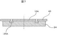
これまで説明してきた静電チャックの表面は一様の状態を想定したものだったが、試料とダミー試料との僅かな隙間でも吸着力が発生している為、異物を引き寄せてしまう。この対策として本発明では図7及び図8に示す静電チャックを提案する。 The surface of the electrostatic chuck described so far has been assumed to be uniform. However, since a suction force is generated even in a slight gap between the sample and the dummy sample, foreign matter is attracted. As a countermeasure, the present invention proposes an electrostatic chuck shown in FIGS.
図7に示す静電チャック24のダミー試料40とφ200mmウエハ10Aの隙間付近は、吸着面をマスク部材24Aにより覆い、吸着力を除去している。φ200mmウエハ10A、及びダミー試料40を静電チャック24に吸着した状態を示している。ここで、マスク部材24Aの幅はφ200mmウエハ10Aとダミー試料40の隙間よりも大きくなるよう設計することで、異物の吸着を確実に除去することが可能となる。 In the vicinity of the gap between the
一方、図8に示す静電チャック24のダミー試料40とφ200mmウエハ10Aの隙間付近は、溝部24Bが形成されている為、仮に異物を吸着してもφ300mmウエハを吸着した場合でも、ウエハを変形させることはない。この溝部24Bの幅もφ200mmウエハ10Aとダミー試料40の隙間よりも大きくなるよう設計することで、異物の吸着を確実に除去することが可能となる。 On the other hand, since a groove 24B is formed in the vicinity of the gap between the
次に、本発明の搬送機構について図9を参照しつつ説明する。
ロードロック3には真空ロボット31が内包されており、試料10及びダミー試料40の搬送を行う。ロードロック3にはダミー試料40を少なくても1枚以上収納可能なストッカー60が取付けられており、試料サイズ毎、材質毎、或いは予備品のダミー試料を待機させることが可能となる。これにより、試料サイズの切替え、予備品への交換が迅速に実行できることから、装置の稼動率低下を抑えることが可能となる。
以上説明した内容において、試料サイズは、例として挙げたφ200mmウエハ、φ300mmウエハの他にも対応できることは言うまでもない。Next, the transport mechanism of the present invention will be described with reference to FIG.
A
In the contents described above, it goes without saying that the sample size can correspond to the φ200 mm wafer and φ300 mm wafer mentioned above as examples.
以上述べてきたように本発明によれば、原価のアップを抑えつつ、異なるサイズの試料を静電吸着可能とし、且つ試料エッジ部の電界を均一化させることで像質を向上させることが可能となる。 As described above, according to the present invention, it is possible to improve the image quality by making it possible to electrostatically attract samples of different sizes while making the electric field of the sample edge uniform while suppressing an increase in cost. It becomes.
1…カラム、2…試料室、3…ロードロック、4…マウント、5…真空ポンプ、6…架台、10…試料、10A…φ200mmウエハ、10B…φ300mmウエハ、11…電子銃、12…電子線、13…電子レンズ、14…偏向器、14A…位置偏向器、14B…走査偏向器、15…検出器、16…電子レンズ、17…偏向制御部、21…ステージ、22…バーミラー、23…干渉計、24…静電チャック、24A…マスク部材、24B…溝部、25…Zセンサ、26…トップテーブル、26A…基準平面部、27…支柱、28…可動テーブル、31…搬送ロボット、32…真空側ゲートバルブ、33…大気側ゲートバルブ、40…ダミー試料、40A…ノッチ用突起、40B…外周用突起、40C…ノッチ、40D…φ200mm用可動ピン、40E…アース突起、41…試料アーム、42…ダミーアーム、43…アース機構、50…ノッチ用基準ピン、51…外周用基準ピン、52…φ300mm用可動ピン、60…ストッカー、61…予備排気室、70…カラム制御部、71…位置制御部、72…ステージ制御部、73…画像制御部、74…モニタ。DESCRIPTION OF SYMBOLS 1 ... Column, 2 ... Sample chamber, 3 ... Load lock, 4 ... Mount, 5 ... Vacuum pump, 6 ... Mount, 10 ... Sample, 10A ... φ200mm wafer, 10B ... φ300mm wafer, 11 ... Electron gun, 12 ... Electron beam , 13 ... Electronic lens, 14 ... Deflector, 14A ... Position deflector, 14B ... Scanning deflector, 15 ... Detector, 16 ... Electronic lens, 17 ... Deflection controller, 21 ... Stage, 22 ... Bar mirror, 23 ...
Claims (14)
Translated fromJapanese前記ステージ上に、設けられた試料保持手段とを備え、
前記試料保持手段は、
第1の試料サイズを有する第1の試料と、前記第1の試料サイズより大きな試料サイズを有する第2の試料との少なくても2種類の試料サイズが載置可能な静電チャックと、
前記静電チャックを搭載する開口部が設けられたトップテーブルと、を有し、
前記開口部の外周部には、前記静電チャック上に載置された前記第2の試料の外周部を囲むように配置された側壁と、該側壁上端に設けられた基準平面部を有し、
前記第1の試料を搭載する場合には、前記静電チャック上に着脱可能なダミー試料を搭載することを特徴とする荷電粒子線装置。A stage for moving the sample;
A sample holding means provided on the stage;
The sample holding means is
An electrostatic chuck capable of mounting at least two sample sizes, a first sample having a first sample size and a second sample having a sample size larger than the first sample size;
A top table provided with an opening for mounting the electrostatic chuck;
The outer peripheral portion of the opening has a side wall disposed so as to surround the outer peripheral portion of the second sample placed on the electrostatic chuck, and a reference plane portion provided at the upper end of the side wall. ,
A charged particle beam apparatus characterized by mounting a detachable dummy sample on the electrostatic chuck when mounting the first sample.
前記着脱可能なダミー試料は、前記静電チャック上の前記第1の試料の外周部と前記側壁との間に生じた空き領域に搭載されることを特徴とする荷電粒子線装置。In claim 1,
The charged particle beam apparatus, wherein the detachable dummy sample is mounted in a vacant region formed between the outer peripheral portion of the first sample and the side wall on the electrostatic chuck.
前記静電チャックのサイズは、前記第1の試料サイズより大きく、前記第2の試料サイズより小さいことを特徴とする荷電粒子線装置。In claim 1,
The charged particle beam apparatus according to claim 1, wherein a size of the electrostatic chuck is larger than the first sample size and smaller than the second sample size.
前記基準平面部の表面と前記第2の試料の表面のそれぞれの高さは、ほぼ同一であることを特徴とする荷電粒子線装置。In claim 1,
The charged particle beam apparatus characterized in that the height of the surface of the reference plane part and the surface of the second sample are substantially the same.
前記ステージ上に、設けられた試料保持手段とを備え、
前記試料保持手段は、
第1の試料サイズを有する第1の試料と、前記第1の試料サイズより大きな試料サイズを有する第2の試料との少なくても2種類の試料サイズが載置可能な静電チャックと、
前記静電チャックを搭載する開口部が設けられたトップテーブルと、を有し、
前記開口部の外周部には、前記静電チャック上に載置された前記第2の試料の外周部を囲むように配置された側壁と、該側壁上端に設けられた基準平面部を有し、
前記第1の試料を搭載する場合には、前記静電チャック上の前記第1の試料の外周部と前記側壁との間に生じた空き領域に着脱可能なダミー試料を搭載し、
前記着脱可能なダミー試料の内径は、前記第1の試料サイズの外径より大きく、前記着脱可能なダミー試料の外径は、前記静電チャックの外径より大きく、かつ前記開口部の外径より小さいことを特徴とする荷電粒子線装置。A stage for moving the sample;
A sample holding means provided on the stage;
The sample holding means is
An electrostatic chuck capable of mounting at least two sample sizes, a first sample having a first sample size and a second sample having a sample size larger than the first sample size;
A top table provided with an opening for mounting the electrostatic chuck;
The outer peripheral portion of the opening has a side wall disposed so as to surround the outer peripheral portion of the second sample placed on the electrostatic chuck, and a reference plane portion provided at the upper end of the side wall. ,
When mounting the first sample, a dummy sample that can be attached to and detached from an empty region formed between the outer peripheral portion of the first sample and the side wall on the electrostatic chuck is mounted,
An inner diameter of the removable dummy sample is larger than an outer diameter of the first sample size, an outer diameter of the removable dummy sample is larger than an outer diameter of the electrostatic chuck, and an outer diameter of the opening. A charged particle beam device characterized by being smaller.
前記着脱可能なダミー試料の厚さは、前記第1の試料もしくは前記第2の試料の厚さとほぼ同一であることを特徴とする荷電粒子線装置。In claim 5,
The charged particle beam apparatus according to claim 1, wherein a thickness of the detachable dummy sample is substantially the same as a thickness of the first sample or the second sample.
前記着脱可能なダミー試料の材質は、前記第1の試料もしくは前記第2の試料と同じ材質であることを特徴とする荷電粒子線装置。In claim 5,
The charged particle beam apparatus according to claim 1, wherein a material of the detachable dummy sample is the same material as the first sample or the second sample.
前記着脱可能なダミー試料は、帯電防止を目的としたアースに接触されていることを特徴とする荷電粒子線装置。In claim 5,
The charged particle beam apparatus, wherein the detachable dummy sample is in contact with a ground for the purpose of preventing charging.
前記着脱可能なダミー試料には、所定のパターンが形成されていることを特徴とする荷電粒子線装置。In claim 5,
A charged particle beam apparatus in which a predetermined pattern is formed on the detachable dummy sample.
前記ステージ上に、設けられた試料保持手段と、
前記ステージを囲むように設けられた試料室と、を備え、
前記試料保持手段は、
第1の試料サイズを有する第1の試料と、前記第1の試料サイズより大きな試料サイズを有する第2の試料との少なくても2種類の試料サイズが載置可能な静電チャックと、
前記静電チャックを搭載する開口部が設けられたトップテーブルと、を有し、
前記第1の試料を搭載する場合には、前記静電チャック上に着脱可能なダミー試料を搭載することを特徴とする荷電粒子線装置。A stage for moving the sample;
Sample holding means provided on the stage;
A sample chamber provided to surround the stage,
The sample holding means is
An electrostatic chuck capable of mounting at least two sample sizes, a first sample having a first sample size and a second sample having a sample size larger than the first sample size;
A top table provided with an opening for mounting the electrostatic chuck;
A charged particle beam apparatus characterized by mounting a detachable dummy sample on the electrostatic chuck when mounting the first sample.
前記着脱可能なダミー試料と前記第1の試料もしくは前記第2の試料が、各々個別に前記ステージから着脱可能な搬送機構を有していることを特徴とする荷電粒子線装置。In claim 10,
The charged particle beam apparatus characterized in that the detachable dummy sample and the first sample or the second sample have a transport mechanism that can be individually detached from the stage.
前記静電チャックの表面付近には、前記第1の試料の外周部と前記着脱可能なダミー試料との間に生じる間隙を延伸した領域を含むように溝部、あるいは非吸着部を設けていることを特徴とする荷電粒子線装置。In claim 10,
Near the surface of the electrostatic chuck, a groove portion or a non-adsorption portion is provided so as to include a region where a gap generated between the outer peripheral portion of the first sample and the detachable dummy sample is extended. Charged particle beam device characterized by the above.
前記第1の試料もしくは前記第2の試料試料と、前記着脱可能なダミー試料を、前記ステージ上で位置決めする位置決め手段を具備していることを特徴とする荷電粒子線装置。In claim 10,
A charged particle beam apparatus comprising positioning means for positioning the first sample or the second sample sample and the detachable dummy sample on the stage.
前記資料室に隣接して設けられ、少なくても1枚以上の着脱可能なダミー試料を収納可能なストッカーを有し、
処理する試料サイズ、材質に応じて着脱可能なダミー試料を選択可能な搬送手段を備えていることを特徴とする荷電粒子線装置。In claim 10,
Provided adjacent to the material room, and having a stocker capable of storing at least one or more removable dummy samples;
A charged particle beam apparatus comprising a transport unit capable of selecting a detachable dummy sample according to a sample size and a material to be processed.
Priority Applications (3)
| Application Number | Priority Date | Filing Date | Title |
|---|---|---|---|
| JP2007156357AJP2008311351A (en) | 2007-06-13 | 2007-06-13 | Charged particle beam equipment |
| US12/137,128US7763863B2 (en) | 2007-06-13 | 2008-06-11 | Charged particle beam application apparatus |
| US12/828,781US8158955B2 (en) | 2007-06-13 | 2010-07-01 | Charged particle beam application apparatus |
Applications Claiming Priority (1)
| Application Number | Priority Date | Filing Date | Title |
|---|---|---|---|
| JP2007156357AJP2008311351A (en) | 2007-06-13 | 2007-06-13 | Charged particle beam equipment |
Publications (2)
| Publication Number | Publication Date |
|---|---|
| JP2008311351Atrue JP2008311351A (en) | 2008-12-25 |
| JP2008311351A5 JP2008311351A5 (en) | 2009-07-30 |
Family
ID=40131437
Family Applications (1)
| Application Number | Title | Priority Date | Filing Date |
|---|---|---|---|
| JP2007156357APendingJP2008311351A (en) | 2007-06-13 | 2007-06-13 | Charged particle beam equipment |
Country Status (2)
| Country | Link |
|---|---|
| US (2) | US7763863B2 (en) |
| JP (1) | JP2008311351A (en) |
Cited By (5)
| Publication number | Priority date | Publication date | Assignee | Title |
|---|---|---|---|---|
| WO2011001586A1 (en)* | 2009-07-03 | 2011-01-06 | 株式会社 日立ハイテクノロジーズ | Charged particle beam apparatus and method for stably obtaining charged particle beam image |
| JP2015026553A (en)* | 2013-07-29 | 2015-02-05 | 株式会社日立ハイテクノロジーズ | Charged particle beam equipment |
| JP2015095542A (en)* | 2013-11-12 | 2015-05-18 | 株式会社ディスコ | Positioning table |
| US9601307B2 (en) | 2013-03-15 | 2017-03-21 | Hitachi High-Technologies Corporation | Charged particle radiation apparatus |
| JP2020009880A (en)* | 2018-07-06 | 2020-01-16 | 株式会社日立ハイテクマニファクチャ&サービス | Substrate holder and scanning electron microscope |
Families Citing this family (13)
| Publication number | Priority date | Publication date | Assignee | Title |
|---|---|---|---|---|
| JP2008311351A (en)* | 2007-06-13 | 2008-12-25 | Hitachi High-Technologies Corp | Charged particle beam equipment |
| JP2009302415A (en)* | 2008-06-17 | 2009-12-24 | Hitachi High-Technologies Corp | Charged-particle beam device, test piece holding system, method for holding test piece, and method for detaching test piece |
| TWI465708B (en)* | 2008-12-29 | 2014-12-21 | Ind Tech Res Inst | Method of processing objects by focused ion beam system and carrier used therewith |
| WO2010097858A1 (en)* | 2009-02-27 | 2010-09-02 | 株式会社 日立ハイテクノロジーズ | Electron microscope, and specimen holding method |
| JP5881686B2 (en)* | 2010-06-08 | 2016-03-09 | アクセリス テクノロジーズ, インコーポレイテッド | Heated electrostatic chuck with the ability to mechanically fix at high temperatures |
| JP5331828B2 (en)* | 2011-01-14 | 2013-10-30 | 株式会社日立ハイテクノロジーズ | Charged particle beam equipment |
| KR102489065B1 (en) | 2013-03-15 | 2023-01-13 | 어플라이드 머티어리얼스, 인코포레이티드 | Position and temperature monitoring of ald platen susceptor |
| JP6496184B2 (en)* | 2014-06-27 | 2019-04-03 | 日本電子株式会社 | Sample introduction method, sample stage, and charged particle beam apparatus |
| US9449805B2 (en)* | 2014-09-23 | 2016-09-20 | Agilent Technologies Inc. | Isolation of charged particle optics from vacuum chamber deformations |
| US10186446B2 (en)* | 2016-09-30 | 2019-01-22 | Axcelis Technology, Inc. | Adjustable circumference electrostatic clamp |
| JP2019215957A (en)* | 2018-06-11 | 2019-12-19 | 株式会社荏原製作所 | Beam bender |
| JP2020199517A (en)* | 2019-06-07 | 2020-12-17 | ファナック株式会社 | Laser machining system |
| CN110982686B (en)* | 2019-12-27 | 2025-01-17 | 珠海迪尔生物工程股份有限公司 | Microorganism observation test card, observation system and observation method |
Citations (2)
| Publication number | Priority date | Publication date | Assignee | Title |
|---|---|---|---|---|
| JP2004079516A (en)* | 1998-04-20 | 2004-03-11 | Hitachi Ltd | Sample holding machine, semiconductor manufacturing device, semiconductor inspection device, and sample holding method |
| JP2004363085A (en)* | 2003-05-09 | 2004-12-24 | Ebara Corp | Inspection apparatus by charged particle beam and method for manufacturing device using inspection apparatus |
Family Cites Families (33)
| Publication number | Priority date | Publication date | Assignee | Title |
|---|---|---|---|---|
| US4789294A (en)* | 1985-08-30 | 1988-12-06 | Canon Kabushiki Kaisha | Wafer handling apparatus and method |
| US5556204A (en)* | 1990-07-02 | 1996-09-17 | Hitachi, Ltd. | Method and apparatus for detecting the temperature of a sample |
| US5539609A (en)* | 1992-12-02 | 1996-07-23 | Applied Materials, Inc. | Electrostatic chuck usable in high density plasma |
| US5350479A (en)* | 1992-12-02 | 1994-09-27 | Applied Materials, Inc. | Electrostatic chuck for high power plasma processing |
| KR100238629B1 (en)* | 1992-12-17 | 2000-01-15 | 히가시 데쓰로 | Stage having eletrostatic chuck and plasma processing apparatus using same |
| US5822171A (en)* | 1994-02-22 | 1998-10-13 | Applied Materials, Inc. | Electrostatic chuck with improved erosion resistance |
| US5631803A (en)* | 1995-01-06 | 1997-05-20 | Applied Materials, Inc. | Erosion resistant electrostatic chuck with improved cooling system |
| US5535090A (en)* | 1994-03-03 | 1996-07-09 | Sherman; Arthur | Electrostatic chuck |
| TW295677B (en)* | 1994-08-19 | 1997-01-11 | Tokyo Electron Co Ltd | |
| US5572398A (en)* | 1994-11-14 | 1996-11-05 | Hewlett-Packard Co. | Tri-polar electrostatic chuck |
| JP3208044B2 (en)* | 1995-06-07 | 2001-09-10 | 東京エレクトロン株式会社 | Plasma processing apparatus and plasma processing method |
| US5781400A (en)* | 1995-09-20 | 1998-07-14 | Hitachi, Ltd. | Electrostatically attracting electrode and a method of manufacture thereof |
| US6370007B2 (en)* | 1995-09-20 | 2002-04-09 | Hitachi, Ltd. | Electrostatic chuck |
| TW334609B (en)* | 1996-09-19 | 1998-06-21 | Hitachi Ltd | Electrostatic chuck, method and device for processing sanyle use the same |
| US6077357A (en)* | 1997-05-29 | 2000-06-20 | Applied Materials, Inc. | Orientless wafer processing on an electrostatic chuck |
| JP3463599B2 (en) | 1998-04-20 | 2003-11-05 | 株式会社日立製作所 | Sample holder, semiconductor manufacturing equipment, semiconductor inspection equipment, circuit pattern inspection equipment, charged particle beam application equipment, calibration substrate, sample holding method, circuit pattern inspection method, and charged particle beam application method |
| US6509564B1 (en)* | 1998-04-20 | 2003-01-21 | Hitachi, Ltd. | Workpiece holder, semiconductor fabricating apparatus, semiconductor inspecting apparatus, circuit pattern inspecting apparatus, charged particle beam application apparatus, calibrating substrate, workpiece holding method, circuit pattern inspecting method, and charged particle beam application method |
| KR100521290B1 (en)* | 1998-06-24 | 2005-10-17 | 가부시키가이샤 히타치세이사쿠쇼 | Dry-etching device and method of producing semiconductor devices |
| JP4151749B2 (en)* | 1998-07-16 | 2008-09-17 | 東京エレクトロンAt株式会社 | Plasma processing apparatus and method |
| JP2001057359A (en)* | 1999-08-17 | 2001-02-27 | Tokyo Electron Ltd | Plasma processing device |
| US6490144B1 (en)* | 1999-11-29 | 2002-12-03 | Applied Materials, Inc. | Support for supporting a substrate in a process chamber |
| KR100502268B1 (en)* | 2000-03-01 | 2005-07-22 | 가부시끼가이샤 히다치 세이사꾸쇼 | Plasma processing apparatus and method |
| TW483037B (en)* | 2000-03-24 | 2002-04-11 | Hitachi Ltd | Semiconductor manufacturing apparatus and method of processing semiconductor wafer using plasma, and wafer voltage probe |
| US6646233B2 (en)* | 2002-03-05 | 2003-11-11 | Hitachi High-Technologies Corporation | Wafer stage for wafer processing apparatus and wafer processing method |
| JP3905462B2 (en)* | 2002-11-20 | 2007-04-18 | 東京エレクトロン株式会社 | Plasma processing method and plasma processing apparatus |
| US6903338B2 (en) | 2003-01-30 | 2005-06-07 | Kla-Tencor Technologies Corporation | Method and apparatus for reducing substrate edge effects in electron lenses |
| US6825617B2 (en)* | 2003-02-27 | 2004-11-30 | Hitachi High-Technologies Corporation | Semiconductor processing apparatus |
| US7138629B2 (en)* | 2003-04-22 | 2006-11-21 | Ebara Corporation | Testing apparatus using charged particles and device manufacturing method using the testing apparatus |
| JP4637684B2 (en)* | 2004-09-10 | 2011-02-23 | 株式会社日立ハイテクノロジーズ | Charged particle beam application equipment |
| JP4997842B2 (en)* | 2005-10-18 | 2012-08-08 | 東京エレクトロン株式会社 | Processing equipment |
| JP4935149B2 (en)* | 2006-03-30 | 2012-05-23 | 東京エレクトロン株式会社 | Electrode plate for plasma processing and plasma processing apparatus |
| US8177990B2 (en)* | 2006-03-31 | 2012-05-15 | Tokyo Electron Limited | Etching method, plasma processing system and storage medium |
| JP2008311351A (en)* | 2007-06-13 | 2008-12-25 | Hitachi High-Technologies Corp | Charged particle beam equipment |
- 2007
- 2007-06-13JPJP2007156357Apatent/JP2008311351A/enactivePending
- 2008
- 2008-06-11USUS12/137,128patent/US7763863B2/ennot_activeExpired - Fee Related
- 2010
- 2010-07-01USUS12/828,781patent/US8158955B2/ennot_activeExpired - Fee Related
Patent Citations (2)
| Publication number | Priority date | Publication date | Assignee | Title |
|---|---|---|---|---|
| JP2004079516A (en)* | 1998-04-20 | 2004-03-11 | Hitachi Ltd | Sample holding machine, semiconductor manufacturing device, semiconductor inspection device, and sample holding method |
| JP2004363085A (en)* | 2003-05-09 | 2004-12-24 | Ebara Corp | Inspection apparatus by charged particle beam and method for manufacturing device using inspection apparatus |
Cited By (8)
| Publication number | Priority date | Publication date | Assignee | Title |
|---|---|---|---|---|
| WO2011001586A1 (en)* | 2009-07-03 | 2011-01-06 | 株式会社 日立ハイテクノロジーズ | Charged particle beam apparatus and method for stably obtaining charged particle beam image |
| JP2011014414A (en)* | 2009-07-03 | 2011-01-20 | Hitachi High-Technologies Corp | Charged particle beam device and method for stably obtaining charged particle beam image |
| US8536540B2 (en) | 2009-07-03 | 2013-09-17 | Hitachi High-Technologies Corporation | Charged particle beam apparatus and method for stably obtaining charged particle beam image |
| US9601307B2 (en) | 2013-03-15 | 2017-03-21 | Hitachi High-Technologies Corporation | Charged particle radiation apparatus |
| JP2015026553A (en)* | 2013-07-29 | 2015-02-05 | 株式会社日立ハイテクノロジーズ | Charged particle beam equipment |
| JP2015095542A (en)* | 2013-11-12 | 2015-05-18 | 株式会社ディスコ | Positioning table |
| JP2020009880A (en)* | 2018-07-06 | 2020-01-16 | 株式会社日立ハイテクマニファクチャ&サービス | Substrate holder and scanning electron microscope |
| JP6994437B2 (en) | 2018-07-06 | 2022-01-14 | 株式会社日立ハイテク | Substrate holder and scanning electron microscope device |
Also Published As
| Publication number | Publication date |
|---|---|
| US20080308743A1 (en) | 2008-12-18 |
| US20100264330A1 (en) | 2010-10-21 |
| US7763863B2 (en) | 2010-07-27 |
| US8158955B2 (en) | 2012-04-17 |
Similar Documents
| Publication | Publication Date | Title |
|---|---|---|
| JP2008311351A (en) | Charged particle beam equipment | |
| CN101630623B (en) | Inspection apparatus by charged particle beam and method for manufacturing device using inspection apparatus | |
| US7248353B2 (en) | Method and apparatus for inspecting samples, and method for manufacturing devices using method and apparatus for inspecting samples | |
| JP5090255B2 (en) | STEM sample preparation method in situ | |
| KR102145469B1 (en) | Inspection apparatus | |
| US7586093B2 (en) | Apparatus and method for inspecting a sample of a specimen by means of an electron beam | |
| JP2005249745A (en) | Sample surface inspecting method and inspecting apparatus | |
| KR20030029045A (en) | Charged particle beam inspection apparatus and method for fabricating device using that inspection apparatus | |
| US9401297B2 (en) | Electrostatic chuck mechanism and charged particle beam apparatus | |
| US9105446B2 (en) | Charged particle beam apparatus | |
| KR102641280B1 (en) | Method for measuring critical dimensions on a substrate, and apparatus for inspecting and cutting electronic devices on the substrate | |
| KR102329264B1 (en) | A method for automated critical dimension measurement of a substrate for manufacturing a display, a method for inspecting a large-area substrate for manufacturing a display, an apparatus for inspecting a large-area substrate for manufacturing a display, and a method of operating the same | |
| JP4875905B2 (en) | Sample holding device and charged particle beam device | |
| US20090309043A1 (en) | Charged particle beam apparatus and sample holding system | |
| WO2018154705A1 (en) | Charged particle beam device | |
| TWI761997B (en) | Sheet manufacturing method, analysis system, and sample analysis method | |
| JP7387880B2 (en) | Tweezers, transport device, and method of transporting sample pieces | |
| JP5302934B2 (en) | Sample surface inspection method and inspection apparatus | |
| JP2006244875A (en) | Mapping projection type electron beam device and defect inspection system using the same | |
| JP6640975B2 (en) | Electrostatic chuck mechanism and charged particle beam device | |
| WO2007086398A1 (en) | Apparatus and method for inspecting sample surface | |
| JP7625017B2 (en) | An emitter for emitting charged particles | |
| JP2003115274A (en) | Sample holding machine, sample holding method, and semiconductor manufacturing apparatus using the same | |
| WO2025119714A1 (en) | Systems and methods of particle contamination reduction in charged-particle beam systems | |
| CN118591769A (en) | Method and apparatus for calibrating operations on a mask |
Legal Events
| Date | Code | Title | Description |
|---|---|---|---|
| A521 | Request for written amendment filed | Free format text:JAPANESE INTERMEDIATE CODE: A523 Effective date:20090615 | |
| A621 | Written request for application examination | Free format text:JAPANESE INTERMEDIATE CODE: A621 Effective date:20090615 | |
| A977 | Report on retrieval | Free format text:JAPANESE INTERMEDIATE CODE: A971007 Effective date:20100615 | |
| A131 | Notification of reasons for refusal | Free format text:JAPANESE INTERMEDIATE CODE: A131 Effective date:20110927 | |
| A02 | Decision of refusal | Free format text:JAPANESE INTERMEDIATE CODE: A02 Effective date:20120207 |