JP2008306004A - Semiconductor device and manufacturing method thereof - Google Patents
Semiconductor device and manufacturing method thereofDownload PDFInfo
- Publication number
- JP2008306004A JP2008306004AJP2007152126AJP2007152126AJP2008306004AJP 2008306004 AJP2008306004 AJP 2008306004AJP 2007152126 AJP2007152126 AJP 2007152126AJP 2007152126 AJP2007152126 AJP 2007152126AJP 2008306004 AJP2008306004 AJP 2008306004A
- Authority
- JP
- Japan
- Prior art keywords
- resistance change
- film
- resistance
- oxide
- region
- Prior art date
- Legal status (The legal status is an assumption and is not a legal conclusion. Google has not performed a legal analysis and makes no representation as to the accuracy of the status listed.)
- Pending
Links
Images


Landscapes
- Semiconductor Memories (AREA)
Abstract
Translated fromJapaneseDescription
Translated fromJapanese本発明は、抵抗素子の電気抵抗の変化に応じて情報を記憶する不揮発性メモリに好適な半導体装置及びその製造方法に関する。 The present invention relates to a semiconductor device suitable for a nonvolatile memory that stores information according to a change in electrical resistance of a resistance element, and a manufacturing method thereof.
従来の不揮発性メモリとしてフラッシュメモリが挙げられる。しかし、フラッシュメモリに対して、32nmノード以降の微細化には、セル間のクロストーク、FG(浮遊ゲート)−CG(制御ゲート)間の容量結合の減少、及びトンネル酸化膜の信頼性等の物理的・本質的な限界が壁となり立ちはだかると予想されている。そこで、近年では、フラッシュメモリとは異なる原理で動作し、より微細化が容易な新規メモリに対する要求が高まっている。そして、外部からの電気的な刺激に応じて抵抗値が変化する物質を用いてデータを記憶する不揮発性メモリセルについての研究が盛んになってきている。このような不揮発性メモリセルを備えたメモリは、抵抗変化メモリとよばれる。このような物質は、その電気的特性に応じて大きく二つに分類することができる。一方は双極性材料とよばれることがあり、他方は単極性材料とよばれることがある。 A flash memory is an example of a conventional nonvolatile memory. However, miniaturization beyond the 32 nm node for flash memory includes crosstalk between cells, reduction of capacitive coupling between FG (floating gate) and CG (control gate), and reliability of tunnel oxide film, etc. It is expected that physical and intrinsic limitations will stand up against the wall. Therefore, in recent years, there is an increasing demand for a new memory that operates on a principle different from that of a flash memory and can be easily miniaturized. Research on nonvolatile memory cells that store data using a substance whose resistance value changes in response to an external electrical stimulus has become active. A memory including such a nonvolatile memory cell is called a resistance change memory. Such substances can be roughly classified into two types according to their electrical characteristics. One is sometimes called a bipolar material and the other is called a unipolar material.
双極性材料としては、Cr等の不純物が微量にドープされたSrTiO3及びSrZrO3が挙げられる。双極性材料からなる薄膜又はバルク材料に、ある閾値以上の電圧を印加すると、抵抗の変化が生じる。但し、変化の前後で抵抗は安定に保たれる。抵抗の変化が生じた後に、逆極性の他の閾値以上の電圧を印加すると、双極性材料の抵抗は元の抵抗と同程度に戻る。このように、双極性材料では、抵抗の変化に互いに極性が異なる電圧の印加が必要である。Examples of the bipolar material include SrTiO3 and SrZrO3 doped with a small amount of impurities such as Cr. When a voltage exceeding a certain threshold is applied to a thin film or bulk material made of a bipolar material, a change in resistance occurs. However, the resistance remains stable before and after the change. After a change in resistance occurs, applying a voltage of another threshold or higher than the reverse polarity will return the resistance of the bipolar material to the same level as the original resistance. As described above, in the bipolar material, it is necessary to apply voltages having different polarities to change the resistance.
双極性材料に負の電圧を印加していくと、ある閾値電圧で電流の絶対値が急増する。つまり、双極性材料の抵抗が高抵抗から低抵抗に急激に変化する。このような高抵抗から低抵抗への切り替わり現象及びその過程はセット(set)とよばれることがある。次に、電圧を正の方向へ掃印していくと、ある閾値電圧で電流の値が急減する。つまり、双極性材料の抵抗が低抵抗から高抵抗に急激に戻る。このような低抵抗から高抵抗への切り替わり現象及びその過程はリセット(reset)とよばれることがある。また、各抵抗は、これらの閾値電圧の間では安定であり、電圧が印加されていなくても保持される。従って、高抵抗の状態及び低抵抗の状態を、夫々「0」及び「1」に対応させることにより、双極性材料をメモリに使用することが可能となる。なお、抵抗が変化する閾値電圧は、材料及び結晶性等に依存する。 When a negative voltage is applied to the bipolar material, the absolute value of the current increases rapidly at a certain threshold voltage. That is, the resistance of the bipolar material changes rapidly from high resistance to low resistance. Such a phenomenon of switching from high resistance to low resistance and the process thereof may be referred to as a set. Next, when the voltage is swept in the positive direction, the current value rapidly decreases at a certain threshold voltage. That is, the resistance of the bipolar material suddenly returns from a low resistance to a high resistance. Such a phenomenon of switching from low resistance to high resistance and the process thereof may be referred to as reset. Each resistor is stable between these threshold voltages and is held even when no voltage is applied. Therefore, by making the high resistance state and the low resistance state correspond to “0” and “1”, respectively, the bipolar material can be used for the memory. Note that the threshold voltage at which the resistance changes depends on the material, crystallinity, and the like.
単極性材料としては、Ni酸化物及びTi酸化物等の単一の遷移金属の酸化物(TMO:Transition Metal Oxide)が挙げられる。単極性材料では、抵抗の変化が印加電圧の極性によらずに生じると共に、低抵抗から高抵抗への変化(reset)が生じる電圧の絶対値が、高抵抗から低抵抗への変化(set)が生じる電圧の絶対値よりも小さい。また、双極性材料と同様に、変化の前後で抵抗は安定に保たれる。従って、高抵抗の状態及び低抵抗の状態を、夫々「0」及び「1」に対応させることにより、単極性材料をメモリに使用することも可能となる。このため、電圧の極性を変えることなく抵抗の大きさを切り替えることが可能である。 Examples of the unipolar material include single transition metal oxides (TMO: Transition Metal Oxide) such as Ni oxide and Ti oxide. In a unipolar material, the change in resistance occurs regardless of the polarity of the applied voltage, and the absolute value of the voltage at which a change from low resistance to high resistance occurs is a change from high resistance to low resistance (set). Is smaller than the absolute value of the voltage. Also, like the bipolar material, the resistance remains stable before and after the change. Accordingly, by making the high resistance state and the low resistance state correspond to “0” and “1”, respectively, it is possible to use a unipolar material for the memory. For this reason, it is possible to switch the magnitude | size of resistance, without changing the polarity of a voltage.
但し、これらの双極性材料及び単極性材料の抵抗の変化は、薄膜等の形成直後から発現するものではなく、薄膜等に比較的大きな電圧を印加することにより、絶縁破壊に類似する現象が生じた後に発現する。このような現象を生じさせる処理はフォーミングとよばれることがある。そして、フォーミングによりフィラメントとよばれる伝導領域が生成され、このフィラメントにおける特性の変化により抵抗が変化すると考えられている。 However, the change in resistance of these bipolar and unipolar materials does not appear immediately after the formation of the thin film or the like, and a phenomenon similar to dielectric breakdown occurs when a relatively large voltage is applied to the thin film or the like. It develops after. Processing that causes such a phenomenon is sometimes called forming. Then, it is considered that a conductive region called a filament is generated by the forming, and the resistance is changed by a change in characteristics of the filament.
このような抵抗変化メモリには、従来のフラッシュメモリと比較して種々の利点がある。例えば、必要とされるプロセス温度が低い。また、微細化が容易である。更に、Siを用いたCMOSロジックへの混載が容易である。そして、近年では、容易に形成することができる単一の遷移金属の酸化物(Ni酸化物及びTi酸化物等)を用いた抵抗変化メモリが特に注目されている。 Such a resistance change memory has various advantages over the conventional flash memory. For example, the required process temperature is low. Moreover, miniaturization is easy. Furthermore, it is easy to mount on CMOS logic using Si. In recent years, a resistance change memory using a single transition metal oxide (such as Ni oxide and Ti oxide) that can be easily formed has attracted particular attention.
しかしながら、本願発明者は、抵抗変化材料としてNi酸化物又はTi酸化物を使用して抵抗変化素子を形成すると、微細化に連れてフォーミングに必要とされる電圧(フォーミング電圧)が大きくなったり、抵抗変化素子の特性が大きくばらついたりしてしまうことを見出した。フォーミング電圧が高くなると、それを見込んで昇圧回路の面積を大きく確保しておく必要が生じたり、抵抗変化素子にトランジスタが接続されている場合には、pn接合又はゲート絶縁膜に破壊が生じたりする。また、フォーミング電圧が高くなると、フォーミグの結果、フィラメントが形成されるだけでなく、完全な絶縁破壊が生じて抵抗変化素子として機能できなくなることもある。 However, the inventor of the present application, when forming a resistance change element using Ni oxide or Ti oxide as a resistance change material, the voltage required for forming (forming voltage) increases with miniaturization, It has been found that the characteristics of the resistance change element vary greatly. When the forming voltage is increased, it is necessary to ensure a large area of the booster circuit in anticipation of this, or when a transistor is connected to the variable resistance element, the pn junction or the gate insulating film may be destroyed. To do. Further, when the forming voltage is increased, not only the filament is formed as a result of the forming, but also a complete dielectric breakdown may occur and the function as a resistance change element may be disabled.
フォーミング電圧の低下という点のみに着目すれば、抵抗変化材料の膜を薄くすることも考えられるが、この場合には、抵抗の変化の繰り返しに対する耐性が低下する可能性がある。また、この膜を挟む2個の電極の材料の熱拡散の影響によって、本来保持されるべき抵抗が変化しやすくなる可能性も高い。 If attention is paid only to the reduction of the forming voltage, it is conceivable to make the film of the resistance change material thin. However, in this case, the resistance to repeated resistance change may be reduced. In addition, there is a high possibility that the resistance to be originally retained is likely to change due to the influence of thermal diffusion of the material of the two electrodes sandwiching this film.
このように、現状では、抵抗変化素子の微細化に伴うフォーミング電圧の変動を効果的に抑制することはできない。 Thus, under the present circumstances, it is not possible to effectively suppress the variation of the forming voltage accompanying the miniaturization of the variable resistance element.
本発明の目的は、微細化に伴うフォーミング電圧の変動を抑制することができる半導体装置及びその製造方法を提供することにある。 An object of the present invention is to provide a semiconductor device and a method for manufacturing the same that can suppress fluctuations in forming voltage due to miniaturization.
本願発明者は、抵抗変化素子の微細化に伴うフォーミング電圧のばらつきの原因について鋭意検討を重ねた結果、次のような見解に至った。 The inventor of the present application has earnestly studied the cause of the variation in forming voltage accompanying the miniaturization of the variable resistance element, and as a result, has reached the following view.
従来の抵抗変化メモリでは、抵抗変化膜が多結晶又はアモルファス相のみから構成されている。また、フィラメントは抵抗変化膜の中で電圧に対して最も弱い部分に生成されると考えられる。但し、電圧に対して最も弱い部分は、抵抗変化膜によって相違している。例えば、抵抗変化膜が多結晶のみから構成されている場合、電圧に対して最も弱い部分は結晶粒界であると考えられるが、結晶粒界の性質は多種多様であり、フィラメントとなる部分は抵抗変化膜毎に相違する。また、抵抗変化膜がアモルファス相のみから構成されている場合には、その内部で原子が不規則に配列しているため、やはりフィラメントになる部分は抵抗変化膜毎に相違する。従って、フォーミング電圧の大きさは、実際にフォーミングを行わなければ特定することができない。 In a conventional resistance change memory, the resistance change film is composed of only a polycrystalline or amorphous phase. In addition, it is considered that the filament is generated at the weakest part with respect to voltage in the resistance change film. However, the weakest part with respect to the voltage differs depending on the resistance change film. For example, when the resistance change film is composed only of polycrystals, the weakest part with respect to the voltage is considered to be the crystal grain boundary, but the nature of the crystal grain boundary is diverse, and the part that becomes the filament is It differs for each resistance change film. In addition, when the variable resistance film is composed only of the amorphous phase, atoms are irregularly arranged inside the film, so that the portion that becomes a filament also differs for each variable resistance film. Therefore, the magnitude of the forming voltage cannot be specified unless the forming is actually performed.
このような状況でも、抵抗変化素子の微細化の程度が小さい場合は、フォーミング電圧のばらつきが小さいのは、抵抗変化膜中での電圧に対する弱さの割合の分布が複数の抵抗変化素子間で同程度になりやすく、フィラメントになる部分の弱さ自体も同程度となっているからであると考えられる。 Even in such a situation, when the degree of miniaturization of the resistance change element is small, the variation in forming voltage is small because the distribution of the ratio of the weakness to the voltage in the resistance change film is between the plurality of resistance change elements. This is because it is likely to be the same level, and the weakness of the part that becomes the filament itself is also the same level.
これに対し、微細化が促進されると、複数の抵抗変化素子間で、抵抗変化膜中での電圧に対する弱さの割合の分布に大きな相違が生じるようになり、フィラメントになる部分の弱さ自体にも大きなばらつきが生じてくる。このため、フォーミング電圧のばらつきが大きくなっていると考えられる。つまり、微細化に伴って、ある抵抗変化素子には含まれる特徴が、他の抵抗変化素子には含まれていないことが多くなっており、フォーミング電圧のばらつきが大きくなっているのである。 On the other hand, when miniaturization is promoted, a large difference occurs in the distribution of the ratio of the weakness to the voltage in the resistance change film among the plurality of resistance change elements, and the weakness of the portion that becomes the filament There will also be large variations in itself. For this reason, it is considered that the variation of the forming voltage is increased. That is, along with miniaturization, the characteristics included in one resistance change element are often not included in other resistance change elements, and the variation in forming voltage increases.
逆の見方をすると、微細化が進められたとしても、電圧に対して最も弱い部分の特徴が各抵抗変化素子の間で同様のものとなっていれば、フォーミング電圧のばらつきが抑制され、また、フォーミング電圧の大きさを予測することが可能となるといえる。 In other words, even if the miniaturization is advanced, if the characteristics of the weakest part with respect to the voltage are the same among the resistance change elements, variations in the forming voltage are suppressed, and It can be said that the magnitude of the forming voltage can be predicted.
そして、本願発明者は、上記見解に基づいて更に鋭意検討を重ねた結果、以下に示す発明の諸態様に想到した。 And as a result of further earnest studies based on the above view, the present inventor has arrived at the following aspects of the invention.
本発明に係る半導体装置には、第1及び第2の電極と、金属酸化物を含有し、その抵抗が前記第1及び第2の電極の間に印加された電圧に伴って変化する抵抗変化部と、が設けられている。そして、前記抵抗変化部中に、組成又は相の少なくとも一方が互いに異なる第1の領域と第2の領域とが混在している。 The semiconductor device according to the present invention includes first and second electrodes and a metal oxide, and a resistance change whose resistance varies with a voltage applied between the first and second electrodes. Are provided. And in the resistance change part, the 1st field and the 2nd field from which at least one of a composition or a phase differs mutually exist.
本発明に係る半導体装置の製造方法では、第1の電極を形成し、その後、前記第1の電極上に、金属酸化物を含有する抵抗変化部を形成する。次に、前記抵抗変化部上に、第2の電極を形成する。なお、前記抵抗変化部として、その中に組成又は相の少なくとも一方が互いに異なる第1の領域と第2の領域とが混在し、その抵抗が前記第1及び第2の電極の間に印加された電圧に伴って変化するものを形成する。 In the method for manufacturing a semiconductor device according to the present invention, a first electrode is formed, and then a resistance change portion containing a metal oxide is formed on the first electrode. Next, a second electrode is formed on the resistance change portion. In addition, as the resistance change portion, a first region and a second region having different compositions or phases are mixed therein, and the resistance is applied between the first and second electrodes. The one that changes with the applied voltage is formed.
本発明によれば、第1の領域と第2の領域との界面が電圧に対して最も弱い部分となるため、フィラメントになる部分の特徴が各抵抗変化素子の間で同様のものとなる。この結果、フォーミング電圧のばらつきを抑制することができる。また、フォーミング電圧の大きさを予測することも可能となる。 According to the present invention, since the interface between the first region and the second region is the weakest part with respect to the voltage, the feature of the part that becomes the filament is the same among the variable resistance elements. As a result, variations in forming voltage can be suppressed. It is also possible to predict the magnitude of the forming voltage.
以下、本発明の実施形態について、添付の図面を参照して具体的に説明する。 Hereinafter, embodiments of the present invention will be specifically described with reference to the accompanying drawings.
(第1の実施形態)
先ず、本発明の第1の実施形態について説明する。図1は、本発明の第1の実施形態に係る半導体装置(抵抗変化メモリ)の構造を示す断面図である。また、図2は、第1の実施形態に係る半導体装置(抵抗変化メモリ)の構造を示すレイアウト図である。(First embodiment)
First, a first embodiment of the present invention will be described. FIG. 1 is a cross-sectional view showing the structure of a semiconductor device (resistance change memory) according to a first embodiment of the present invention. FIG. 2 is a layout diagram showing the structure of the semiconductor device (resistance change memory) according to the first embodiment.
本実施形態では、半導体基板1の表面に、STI(Shallow Trench Isolation)法等により素子分離絶縁膜2が形成されている。半導体基板1の表面の導電型は、例えばp型である。また、半導体基板1上に、ゲート絶縁膜3及びゲート電極4が形成されている。更に、半導体基板1の表面に、平面視でゲート電極4を挟むようにして、導電型がn型のソース5及びドレイン6が形成されている。また、ゲート電極4の側方にサイドウォール絶縁膜7が形成されている。このようにして、トランジスタ30が構成されている。なお、ドレイン6は、トランジスタ30毎に独立して形成されているが、ソース5は、複数のトランジスタ30により共有されている。 In the present embodiment, an element
半導体基板1上に、トランジスタ30を覆う層間絶縁膜8が形成されている。層間絶縁膜8は、例えば酸化シリコンから構成されている。層間絶縁膜8に、ソース5まで到達するコンタクトホール及びドレイン6まで到達するコンタクトホールが形成されており、これらの内部にコンタクトプラグ9が埋め込まれている。コンタクトプラグ9は、例えば、コンタクトホールの側面及び底面上に形成されたバリアメタル膜、及びその上に形成されたW膜とから構成されている。層間絶縁膜8の表面は平坦化されている。 An interlayer insulating
そして、層間絶縁膜8上に、ソース5に接するコンタクトプラグ9に接する信号線14、及びドレイン6に接するコンタクトプラグ9に接するパッド13が形成されている。信号線14及びパッド13は、例えばバリアメタル膜10、その上に形成されたAl膜11及びその上に形成されたバリアメタル膜12の積層体から構成されている。 On the
層間絶縁膜8上に、パッド13及び信号線14を覆う層間絶縁膜15が形成されている。層間絶縁膜15は、例えば酸化シリコンから構成されている。層間絶縁膜15に、パッド13まで到達するコンタクトホールが形成されており、これらの内部にコンタクトプラグ16が埋め込まれている。コンタクトプラグ16は、例えば、コンタクトホールの側面及び底面上に形成されたバリアメタル膜、及びその上に形成されたW膜とから構成されている。層間絶縁膜15の表面は平坦化されている。 On the
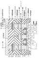
そして、層間絶縁膜15上に、コンタクトプラグ16に接する下部電極17が形成されている。また、下部電極17上に、抵抗変化膜18(抵抗変化部)及び上部電極19がこの順で積層されている。下部電極17、抵抗変化膜18及び上部電極19から抵抗変化素子20が構成されている。例えば、下部電極17及び上部電極19はPtから構成され、これらの厚さは50nm程度である。抵抗変化膜18の詳細については後述する。 A lower electrode 17 in contact with the
層間絶縁膜15上に、抵抗変化素子20を覆う層間絶縁膜21が形成されている。層間絶縁膜21は、例えば酸化シリコンから構成されている。層間絶縁膜21に、抵抗変化素子20まで到達するコンタクトホールが形成されており、この内部にコンタクトプラグ22が埋め込まれている。コンタクトプラグ22は、例えば、コンタクトホールの側面及び底面上に形成されたバリアメタル膜、及びその上に形成されたW膜とから構成されている。層間絶縁膜21の表面は平坦化されている。 An interlayer insulating
そして、層間絶縁膜21上に、複数のコンタクトプラグ22に接するビット線23が形成されている。ビット線23は、例えばAlから構成されている。層間絶縁膜21上には、更に他の層間絶縁膜及び配線等が形成されている。 A
ビット線23は、図2に示すように、複数設けられており、これらは互いに平行に延びている。また、ゲート電極4はワード線として機能し、1本の信号線14が平面視で2つのワード線(ゲート電極4)に挟まれている。図3は、第1の実施形態に係る抵抗変化メモリの構成を示す回路図である。 As shown in FIG. 2, a plurality of
図3に示すように、複数の信号線14が平行に互いに延びており、各信号線14の両側に1本ずつのワード線(ゲート電極4)が位置している。また、複数のビット線23がこれらと交差している。そして、信号線14とビット線23との交点の近傍において、2個のトランジスタ30のソース5が信号線14に共通接続され、これらのトランジスタ30の各ゲート電極4がワード線となっている。また、これらのトランジスタ30のドレイン6に抵抗変化素子20の下部電極17が接続され、抵抗変化素子20の上部電極19がビット線23に接続されている。 As shown in FIG. 3, the plurality of
また、図示しないが、ワード線(ゲート電極4)、信号線14及びビット線23には、抵抗変化膜18の抵抗を変化させることにより、抵抗変化素子20に情報を記憶させる書き込み回路が接続されている。更に、信号線14及びビット線23には、抵抗変化膜18の抵抗を判別することにより、抵抗変化素子20から情報を読み出す読み出し回路も接続されている。 Although not shown, a write circuit that stores information in the
ここで、抵抗変化膜18について詳述する。図4は、第1の実施形態における抵抗変化膜18の詳細を示す断面図である。例えば、抵抗変化膜18の材料はNi酸化物であり、抵抗変化膜18の厚さは20nm程度である。また、抵抗変化膜18は、Ni酸化物のアモルファス領域18a及びNi酸化物の微結晶18bから構成されている。即ち、抵抗変化膜18は異なる2相(アモルファス相及び結晶相)から構成されている。 Here, the
このように構成された抵抗変化メモリでは、抵抗変化膜18中にアモルファス領域18aと微結晶18bとの界面が存在する。従って、比較的大きな電圧が印加されると、この界面の一部に擬似絶縁破壊が生じ、ここにフィラメントが生成される。即ち、フォーミングが行われる。そして、アモルファス領域18aと微結晶18bとの界面の特徴には、あまりばらつきが生じないため、フォーミング電圧のばらつきも小さなものとなる。更に、アモルファス領域18aと微結晶18bとの界面が確実にフィラメントとなるため、フォーミング電圧が異常に上昇することもない。つまり、抵抗変化膜18を、抵抗の変化の繰り返しに対する耐性が低下したり、熱拡散の影響を受けやすくなったりするほど薄くせずとも、適切な電圧でフォーミングを行うことが可能である。 In the resistance change memory configured as described above, an interface between the
次に、第1の実施形態に係る抵抗変化メモリを製造する方法について説明する。図5A乃至図5Fは、第1の実施形態に係る抵抗変化メモリを製造する方法を工程順に示す断面図である。 Next, a method for manufacturing the resistance change memory according to the first embodiment will be described. 5A to 5F are cross-sectional views illustrating a method of manufacturing the resistance change memory according to the first embodiment in the order of steps.
先ず、図1に示すように、半導体基板1の表面に素子分離絶縁膜2を形成する。次に、素子分離絶縁膜2により画定された素子活性領域内に、トランジスタ30を形成する。次いで、層間絶縁膜8、コンタクトプラグ9、パッド13及び信号線14、層間絶縁膜15、並びにコンタクトプラグ16をこの順で形成する。 First, as shown in FIG. 1, an element
次に、図5Aに示すように、例えば、DCスパッタ法により、温度:300℃、パワー:1kW、雰囲気:Ar雰囲気、圧力:0.5Paの条件下で、Pt膜17aを50nm程度の厚さで層間絶縁膜15及びコンタクトプラグ16上に形成する。なお、Pt膜17aの層間絶縁膜15との密着性が十分でない場合(例えば、層間絶縁膜15がシリコン酸化膜の場合)には、Pt膜17aを形成する前に、密着層及び拡散防止層として、厚さが5nm程度のTi膜及び厚さが10nm程度のTiN膜を形成しておくことが好ましい。Ti膜は、例えば、DCスパッタ法により、温度:50℃、パワー:1kW、雰囲気:Ar雰囲気、圧力:0.5Paの条件下で形成することができる。また、TiN膜は、例えば、DC反応性スパッタ法により、温度:300℃、パワー:2kW、雰囲気:Ar/N2混合雰囲気、Arの分圧:0.25Pa、N2の分圧:0.25Paの条件下で形成することができる。Next, as shown in FIG. 5A, the
次いで、図5Bに示すように、例えば、RFスパッタ法により、温度:50℃、パワー:1kW、雰囲気:Ar/O2混合雰囲気、Arの分圧:0.45Pa、O2の分圧:0.05Paの条件下で、アモルファスNi酸化膜18cを20nm程度の厚さでPt膜17a上に形成する。なお、アモルファスNi酸化膜18cを、Niターゲットを用いたAr/O2混合雰囲気中でのDCリアクティブスパッタ法、又はNiOターゲットを用いたAr/O2混合雰囲気中でのRFリアクティブスパッタ法により形成してもよい。成膜温度を50℃と低温にし、特に基板バイアス等の特殊な条件を加えない限り、アモルファス状態のNi酸化膜が得られる。Next, as shown in FIG. 5B, for example, by RF sputtering, temperature: 50 ° C., power: 1 kW, atmosphere: Ar / O2 mixed atmosphere, Ar partial pressure: 0.45 Pa, O2 partial pressure: 0 An amorphous Ni oxide film 18c is formed on the
その後、図5Cに示すように、温度:400℃、雰囲気:N2雰囲気、圧力:101325Pa(1atm)、時間:30分の条件下で、熱処理を行うことにより、アモルファスNi酸化膜18cの一部を結晶化させる。この結果、アモルファス領域18a及び微結晶18bからなる抵抗変化膜18が得られる。Thereafter, as shown in FIG. 5C, a part of the amorphous Ni oxide film 18c is formed by performing heat treatment under the conditions of temperature: 400 ° C., atmosphere: N2 atmosphere, pressure: 101325 Pa (1 atm), time: 30 minutes. Crystallize. As a result, the
続いて、図5Dに示すように、例えば、DCスパッタ法により、温度:50℃、パワー:1kW、雰囲気:Ar雰囲気、圧力:0.5Paの条件下で、Pt膜19aを50nm程度の厚さで抵抗変化膜18上に形成する。 Subsequently, as shown in FIG. 5D, the
次に、図5Eに示すように、フォトリソグラフィ技術により、Pt膜17a、抵抗変化膜18及びPt膜19aのうちの抵抗変化素子20を形成する予定の部分を覆うレジストパターン31を形成する。 Next, as shown in FIG. 5E, a resist pattern 31 is formed by photolithography to cover a portion of the
次いで、図5Fに示すように、レジストパターン31をマスクとして、Pt膜17a、抵抗変化膜18及びPt膜19aに対するドライエッチングを行う。この結果、Pt膜17aから下部電極17が得られ、Pt膜19aから上部電極19が得られる。そして、レジストパターン31を除去する。 Next, as shown in FIG. 5F, dry etching is performed on the
その後、層間絶縁膜21等を形成し、抵抗変化メモリを完成させる。このように、この製造方法では、抵抗変化膜18の形成に当たり、ナノクリスタル技術とよばれる技術を採用している。 Thereafter, the
なお、抵抗変化膜18の材料はNi酸化物に限定されることはなく、Ti酸化物、Ta酸化物、Hf酸化物、Zr酸化物、Y酸化物、Ce酸化物、Mg酸化物、Zn酸化物、W酸化物、Nb酸化物、Cr酸化物、Mn酸化物、Al酸化物、V酸化物、Co酸化物、Cu酸化物等の電圧パルスにより抵抗変化を示す金属酸化物(特に、遷移金属酸化物)を用いてもよい。また、抵抗変化膜18の形成に際し、微結晶18bのサイズ及び密度は、材料及び熱処理の条件に依存する。従って、材料及び熱処理の条件を適切に選択することにより、所望の絶縁性及びフォーミング電圧を得ることができる。 The material of the
(第2の実施形態)
次に、本発明の第2の実施形態について説明する。第2の実施形態では、抵抗変化膜18の構成が第1の実施形態と相違している。図6は、第2の実施形態における抵抗変化膜18の詳細を示す断面図である。(Second Embodiment)
Next, a second embodiment of the present invention will be described. In the second embodiment, the configuration of the
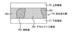
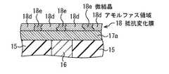
第2の実施形態では、例えば、抵抗変化膜18の材料はNi酸化物及びTi酸化物であり、抵抗変化膜18の厚さは20nm程度である。また、抵抗変化膜18は、Ti酸化物及びNi酸化物のアモルファス領域18d及びNi酸化物の微結晶18eから構成されている。即ち、抵抗変化膜18は異なる2相(アモルファス相及び結晶相)から構成されている。また、第1の実施形態では、アモルファス領域18aと微結晶18bとの間で組成が同一であるが、第2の実施形態では、アモルファス領域18dと微結晶18eとの間で組成が相違している。他の構成は第1の実施形態と同様である。 In the second embodiment, for example, the material of the
このような第2の実施形態によっても第1の実施形態と同様の効果が得られる。 The effect similar to 1st Embodiment is acquired also by such 2nd Embodiment.
次に、第2の実施形態に係る抵抗変化メモリを製造する方法について説明する。図7A乃至図7Fは、第2の実施形態に係る抵抗変化メモリを製造する方法を工程順に示す断面図である。 Next, a method for manufacturing the resistance change memory according to the second embodiment will be described. 7A to 7F are cross-sectional views showing a method of manufacturing the resistance change memory according to the second embodiment in the order of steps.
先ず、第1の実施形態と同様にして、コンタクトプラグ16の形成までの処理を行う。次に、図7Aに示すように、例えば、DCスパッタ法により、温度:300℃、パワー:1kW、雰囲気:Ar雰囲気、圧力:0.5Paの条件下で、Pt膜17aを50nm程度の厚さで層間絶縁膜15及びコンタクトプラグ16上に形成する。なお、Pt膜17aの層間絶縁膜15との密着性が十分でない場合(例えば、層間絶縁膜15がシリコン酸化膜の場合)には、Pt膜17aを形成する前に、密着層及び拡散防止層として、厚さが5nm程度のTi膜及び厚さが10nm程度のTiN膜を形成しておくことが好ましい。Ti膜は、例えば、DCスパッタ法により、温度:50℃、パワー:1kW、雰囲気:Ar雰囲気、圧力:0.5Paの条件下で形成することができる。また、TiN膜は、例えば、DC反応性スパッタ法により、温度:300℃、パワー:2kW、雰囲気:Ar/N2混合雰囲気、Arの分圧:0.25Pa、N2の分圧:0.25Paの条件下で形成することができる。First, similarly to the first embodiment, processing up to the formation of the
次いで、図7Bに示すように、例えば、RFスパッタ法により、温度:50℃、パワー:0.3kW、雰囲気:Ar/O2混合雰囲気、Arの分圧:0.45Pa、O2の分圧:0.05Paの条件下で、アモルファスNi酸化膜を形成しつつ、温度:50℃、パワー:1kW、雰囲気:Ar/O2混合雰囲気、Arの分圧:0.45Pa、O2の分圧:0.05Paの条件下で、アモルファスTi酸化膜を形成する。この結果、Ni酸化物及びTi酸化物からなるアモルファス遷移金属酸化膜18fがPt膜17a上に形成される。アモルファス遷移金属酸化膜18fの厚さは20nm程度とする。なお、アモルファス遷移金属酸化膜18fの形成方法は特に限定されないが、Ni酸化物ターゲット及びTi酸化物ターゲットを用いて2箇所からプラズマを同時に発生させる方法が容易な方法である。但し、アモルファス遷移金属酸化膜18fの組成を予め決めてある場合には、Ni酸化物及びTi酸化物を含有する1個のターゲット(例えば、焼結ターゲット)を用いて1箇所からプラズマを発生させてもよい。Next, as shown in FIG. 7B, for example, by RF sputtering, temperature: 50 ° C., power: 0.3 kW, atmosphere: Ar / O2 mixed atmosphere, Ar partial pressure: 0.45 Pa, O2 partial pressure : Temperature: 50 ° C., power: 1 kW, atmosphere: Ar / O2 mixed atmosphere, Ar partial pressure: 0.45 Pa, O2 partial pressure while forming an amorphous Ni oxide film under the condition of 0.05 Pa : An amorphous Ti oxide film is formed under the condition of 0.05 Pa. As a result, an amorphous transition metal oxide film 18f made of Ni oxide and Ti oxide is formed on the
その後、図7Cに示すように、温度:450℃、雰囲気:N2雰囲気、圧力:101325Pa(1atm)、時間:30分の条件下で、熱処理を行うことにより、アモルファス遷移金属酸化膜18f中のアモルファスNi酸化物の一部を結晶化させる。この結果、Ti酸化物及びNi酸化物から構成されたアモルファス領域18d及びNi酸化物から構成された微結晶18eからなる抵抗変化膜18が得られる。Thereafter, as shown in FIG. 7C, heat treatment is performed under the conditions of temperature: 450 ° C., atmosphere: N2 atmosphere, pressure: 101325 Pa (1 atm), and time: 30 minutes, whereby the amorphous transition metal oxide film 18f A part of the amorphous Ni oxide is crystallized. As a result, an
続いて、図7Dに示すように、例えば、DCスパッタ法により、温度:50℃、パワー:1kW、雰囲気:Ar雰囲気、圧力:0.5Paの条件下で、Pt膜19aを50nm程度の厚さで抵抗変化膜18上に形成する。 Subsequently, as shown in FIG. 7D, the
次に、図7Eに示すように、フォトリソグラフィ技術により、Pt膜17a、抵抗変化膜18及びPt膜19aのうちの抵抗変化素子20を形成する予定の部分を覆うレジストパターン31を形成する。 Next, as shown in FIG. 7E, a resist pattern 31 is formed by photolithography to cover a portion of the
次いで、図7Fに示すように、レジストパターン31をマスクとして、Pt膜17a、抵抗変化膜18及びPt膜19aに対するドライエッチングを行う。この結果、Pt膜17aから下部電極17が得られ、Pt膜19aから上部電極19が得られる。そして、レジストパターン31を除去する。 Next, as shown in FIG. 7F, dry etching is performed on the
その後、層間絶縁膜21等を形成し、抵抗変化メモリを完成させる。このように、この製造方法でも、抵抗変化膜18の形成に当たり、ナノクリスタル技術とよばれる技術を採用している。 Thereafter, the
なお、抵抗変化膜18の材料はNi酸化物及びTi酸化物の組み合わせに限定されることはなく、その一方又は両方に代えて、Ta酸化物、Hf酸化物、Zr酸化物、Y酸化物、Ce酸化物、Mg酸化物、Zn酸化物、W酸化物、Nb酸化物、Cr酸化物、Mn酸化物、Al酸化物、V酸化物、Co酸化物、Cu酸化物等の電圧パルスにより抵抗変化を示す金属酸化物(特に、遷移金属酸化物)を用いてもよい。また、金属酸化物が3種類以上であってもよい。更に、抵抗変化膜18の形成に際し、微結晶18bと同様に、微結晶18eのサイズ及び密度は、材料及び熱処理の条件に依存する。従って、材料及び熱処理の条件を適切に選択することにより、所望の絶縁性及びフォーミング電圧を得ることができる。 The material of the
また、第1及び第2の実施形態では、アモルファス相と結晶相とが混在して抵抗変化膜18が構成されているが、互いに組成が異なる結晶相が混在して抵抗変化膜18が構成されていてもよい。但し、この場合には、組成が相違する結晶間の界面が電圧に対して最も弱い部分となっていることが好ましい。 In the first and second embodiments, the
また、フィラメントとなる界面が抵抗変化膜18を貫通している必要はなく、例えば微結晶18b又は18eが抵抗変化膜18の内部のみに存在していてもよい。 Further, the interface serving as a filament does not need to penetrate the
また、第1及び第2の実施形態では、抵抗変化メモリのスイッチング素子として電界効果トランジスタが用いられているが、これに代えてダイオードを用いてもよい。また、配線がより多数であってもよい。また、抵抗変化素子20及びビット線23がより上層に配置されていてもよい。また、第1及び第2の実施形態では、下部電極17及び上部電極19がPtから構成されているが、他の電極材料を用いてもよい。例えば、Ir、W、Ni、Au、Cu、Ag、Pd、Zn、Cr、Al、Mn、Ta、TaN、Ti、TiN、Ru、RuO2、ITO(Indium-Tin-Oxide)、IrO2、SrRuO3、CoSi2、WSi2、NiSi、MoSi2、TiSi2、Al−Si合金、Al−Cu合金、Al−Si−Cu合金等の、金属、金属化合物又はシリサイドを用いてもよい。更に、コンタクトプラグ9等の材料としてCuを用いてもよい。In the first and second embodiments, the field effect transistor is used as the switching element of the resistance change memory, but a diode may be used instead. Further, the number of wirings may be larger. Further, the
18:抵抗変化膜
18a、18d:アモルファス領域
18b、18e:微結晶
18c:アモルファスNi酸化膜
18f:アモルファス遷移金属酸化膜18:
Claims (6)
Translated fromJapanese金属酸化物を含有し、その抵抗が前記第1及び第2の電極の間に印加された電圧に伴って変化する抵抗変化部と、
を有し、
前記抵抗変化部中に、組成又は相の少なくとも一方が互いに異なる第1の領域と第2の領域とが混在していることを特徴とする半導体装置。First and second electrodes;
A resistance change portion that contains a metal oxide and whose resistance changes with a voltage applied between the first and second electrodes;
Have
The semiconductor device, wherein the resistance change portion includes a first region and a second region having at least one of composition and phase different from each other.
前記第2の領域の相は、結晶相であることを特徴とする請求項1に記載の半導体装置。The phase of the first region is an amorphous phase;
The semiconductor device according to claim 1, wherein the phase of the second region is a crystal phase.
前記第2の領域中の金属酸化物は、1種類であることを特徴とする請求項2に記載の半導体装置。The first region contains a plurality of types of metal oxides,
3. The semiconductor device according to claim 2, wherein the metal oxide in the second region is one kind.
前記第1の電極上に、金属酸化物を含有する抵抗変化部を形成する工程と、
前記抵抗変化部上に、第2の電極を形成する工程と、
を有し、
前記抵抗変化部として、
その中に組成又は相の少なくとも一方が互いに異なる第1の領域と第2の領域とが混在し、
その抵抗が前記第1及び第2の電極の間に印加された電圧に伴って変化するものを形成することを特徴とする半導体装置の製造方法。Forming a first electrode;
Forming a resistance change portion containing a metal oxide on the first electrode;
Forming a second electrode on the variable resistance portion;
Have
As the resistance change section,
The first region and the second region in which at least one of the composition or the phase is different from each other are mixed therein,
A method of manufacturing a semiconductor device, wherein a resistor whose resistance changes with a voltage applied between the first and second electrodes is formed.
前記第1の電極上に、アモルファス状の金属酸化物膜を形成する工程と、
熱処理により、前記金属酸化物膜の一部を結晶化する工程と、
を有することを特徴とする請求項5に記載の半導体装置の製造方法。The step of forming the resistance change portion includes:
Forming an amorphous metal oxide film on the first electrode;
Crystallization of a part of the metal oxide film by heat treatment;
The method of manufacturing a semiconductor device according to claim 5, wherein:
Priority Applications (1)
| Application Number | Priority Date | Filing Date | Title |
|---|---|---|---|
| JP2007152126AJP2008306004A (en) | 2007-06-07 | 2007-06-07 | Semiconductor device and manufacturing method thereof |
Applications Claiming Priority (1)
| Application Number | Priority Date | Filing Date | Title |
|---|---|---|---|
| JP2007152126AJP2008306004A (en) | 2007-06-07 | 2007-06-07 | Semiconductor device and manufacturing method thereof |
Publications (1)
| Publication Number | Publication Date |
|---|---|
| JP2008306004Atrue JP2008306004A (en) | 2008-12-18 |
Family
ID=40234442
Family Applications (1)
| Application Number | Title | Priority Date | Filing Date |
|---|---|---|---|
| JP2007152126APendingJP2008306004A (en) | 2007-06-07 | 2007-06-07 | Semiconductor device and manufacturing method thereof |
Country Status (1)
| Country | Link |
|---|---|
| JP (1) | JP2008306004A (en) |
Cited By (7)
| Publication number | Priority date | Publication date | Assignee | Title |
|---|---|---|---|---|
| JP2009212380A (en)* | 2008-03-05 | 2009-09-17 | Fujitsu Ltd | Resistance change type memory and its manufacturing method |
| JP2010186810A (en)* | 2009-02-10 | 2010-08-26 | Nec Corp | Semiconductor storage device, structure, and manufacturing method |
| JP2014207440A (en)* | 2013-03-18 | 2014-10-30 | パナソニック株式会社 | Nonvolatile storage device and method for manufacturing the same |
| US9356235B2 (en) | 2014-03-25 | 2016-05-31 | Winbond Electronics Corp. | Structure and formation method of memory device |
| US9379320B2 (en) | 2009-07-31 | 2016-06-28 | Kabushiki Kaisha Toshiba | Nonvolatile memory device |
| CN110676374A (en)* | 2019-05-22 | 2020-01-10 | 集美大学 | A kind of resistive memory and preparation method thereof |
| CN116419578A (en)* | 2023-06-12 | 2023-07-11 | 北京大学 | Resistive variable memory with reduced initialization voltage based on local single crystal phase and its preparation |
Citations (4)
| Publication number | Priority date | Publication date | Assignee | Title |
|---|---|---|---|---|
| JP2004241396A (en)* | 2002-02-07 | 2004-08-26 | Sharp Corp | Method of manufacturing variable resistance element, method of manufacturing nonvolatile variable resistance memory device, and nonvolatile variable resistance memory device |
| JP2005203463A (en)* | 2004-01-14 | 2005-07-28 | Sharp Corp | Nonvolatile semiconductor memory device |
| JP2005340786A (en)* | 2004-04-23 | 2005-12-08 | Sharp Corp | Method for forming PCMO thin film having memory resistance characteristics and PCMO device |
| WO2006009218A1 (en)* | 2004-07-22 | 2006-01-26 | Nippon Telegraph And Telephone Corporation | Apparatus for obtaining double stable resistance values, method for manufacturing the same, metal oxide thin film and method for manufacturing the same |
- 2007
- 2007-06-07JPJP2007152126Apatent/JP2008306004A/enactivePending
Patent Citations (4)
| Publication number | Priority date | Publication date | Assignee | Title |
|---|---|---|---|---|
| JP2004241396A (en)* | 2002-02-07 | 2004-08-26 | Sharp Corp | Method of manufacturing variable resistance element, method of manufacturing nonvolatile variable resistance memory device, and nonvolatile variable resistance memory device |
| JP2005203463A (en)* | 2004-01-14 | 2005-07-28 | Sharp Corp | Nonvolatile semiconductor memory device |
| JP2005340786A (en)* | 2004-04-23 | 2005-12-08 | Sharp Corp | Method for forming PCMO thin film having memory resistance characteristics and PCMO device |
| WO2006009218A1 (en)* | 2004-07-22 | 2006-01-26 | Nippon Telegraph And Telephone Corporation | Apparatus for obtaining double stable resistance values, method for manufacturing the same, metal oxide thin film and method for manufacturing the same |
Cited By (8)
| Publication number | Priority date | Publication date | Assignee | Title |
|---|---|---|---|---|
| JP2009212380A (en)* | 2008-03-05 | 2009-09-17 | Fujitsu Ltd | Resistance change type memory and its manufacturing method |
| JP2010186810A (en)* | 2009-02-10 | 2010-08-26 | Nec Corp | Semiconductor storage device, structure, and manufacturing method |
| US9379320B2 (en) | 2009-07-31 | 2016-06-28 | Kabushiki Kaisha Toshiba | Nonvolatile memory device |
| JP2014207440A (en)* | 2013-03-18 | 2014-10-30 | パナソニック株式会社 | Nonvolatile storage device and method for manufacturing the same |
| US9356235B2 (en) | 2014-03-25 | 2016-05-31 | Winbond Electronics Corp. | Structure and formation method of memory device |
| CN110676374A (en)* | 2019-05-22 | 2020-01-10 | 集美大学 | A kind of resistive memory and preparation method thereof |
| CN116419578A (en)* | 2023-06-12 | 2023-07-11 | 北京大学 | Resistive variable memory with reduced initialization voltage based on local single crystal phase and its preparation |
| CN116419578B (en)* | 2023-06-12 | 2023-09-08 | 北京大学 | Resistive switching memory with reduced initialization voltage based on local single crystal phase and its preparation |
Similar Documents
| Publication | Publication Date | Title |
|---|---|---|
| JP5488458B2 (en) | Resistance change element and manufacturing method thereof | |
| CN102013456B (en) | Method for manufacturing memory element | |
| US8168538B2 (en) | Buried silicide structure and method for making | |
| US7903457B2 (en) | Multiple phase change materials in an integrated circuit for system on a chip application | |
| US6569705B2 (en) | Metal structure for a phase-change memory device | |
| US6757190B2 (en) | Single level metal memory cell using chalcogenide cladding | |
| US11101321B2 (en) | Nonvolatile resistive memory device and manufacturing method thereof | |
| TWI387103B (en) | Fully self-aligned pore-type memory cell having diode access device | |
| US8415651B2 (en) | Phase change memory cell having top and bottom sidewall contacts | |
| JP5309615B2 (en) | Resistance change type memory and manufacturing method thereof | |
| US20120292585A1 (en) | Continuous plane of thin-film materials for a two-terminal cross-point memory | |
| JP2008306004A (en) | Semiconductor device and manufacturing method thereof | |
| JP5217259B2 (en) | Semiconductor device and manufacturing method thereof | |
| US9048423B2 (en) | Memory storage device and method of manufacturing the same | |
| JPWO2008107941A1 (en) | Semiconductor device and manufacturing method thereof | |
| KR20050055582A (en) | Rram memory cell electrodes | |
| JP4621817B1 (en) | Nonvolatile memory element and semiconductor memory device including the same | |
| JP2008065953A (en) | Nonvolatile semiconductor memory device and reading method thereof | |
| US20130128654A1 (en) | Nonvolatile memory element, method of manufacturing nonvolatile memory element, method of initial breakdown of nonvolatile memory element, and nonvolatile memory device | |
| JP2006120707A (en) | Variable resistance element and semiconductor device | |
| TWI550621B (en) | Circuit and system of using junction diode as program selector for electrical fuses with extended area for one-time programmable devices | |
| KR100842903B1 (en) | Phase change memory device and manufacturing method thereof | |
| KR20250112592A (en) | Resistance variable memory device and method for fabricating the same | |
| KR100947932B1 (en) | Resistive memory device and manufacturing method thereof | |
| KR20100115880A (en) | Phase-change memory elements and fabrication method thereof |
Legal Events
| Date | Code | Title | Description |
|---|---|---|---|
| A621 | Written request for application examination | Free format text:JAPANESE INTERMEDIATE CODE: A621 Effective date:20100205 | |
| A977 | Report on retrieval | Free format text:JAPANESE INTERMEDIATE CODE: A971007 Effective date:20120613 | |
| A131 | Notification of reasons for refusal | Free format text:JAPANESE INTERMEDIATE CODE: A131 Effective date:20120619 | |
| A521 | Request for written amendment filed | Free format text:JAPANESE INTERMEDIATE CODE: A523 Effective date:20120817 | |
| A02 | Decision of refusal | Free format text:JAPANESE INTERMEDIATE CODE: A02 Effective date:20130205 |