JP2008300384A - Semiconductor device and manufacturing method thereof - Google Patents
Semiconductor device and manufacturing method thereofDownload PDFInfo
- Publication number
- JP2008300384A JP2008300384AJP2007141395AJP2007141395AJP2008300384AJP 2008300384 AJP2008300384 AJP 2008300384AJP 2007141395 AJP2007141395 AJP 2007141395AJP 2007141395 AJP2007141395 AJP 2007141395AJP 2008300384 AJP2008300384 AJP 2008300384A
- Authority
- JP
- Japan
- Prior art keywords
- fin
- type active
- active region
- semiconductor device
- gate electrode
- Prior art date
- Legal status (The legal status is an assumption and is not a legal conclusion. Google has not performed a legal analysis and makes no representation as to the accuracy of the status listed.)
- Abandoned
Links
Images


Classifications
- H—ELECTRICITY
- H10—SEMICONDUCTOR DEVICES; ELECTRIC SOLID-STATE DEVICES NOT OTHERWISE PROVIDED FOR
- H10D—INORGANIC ELECTRIC SEMICONDUCTOR DEVICES
- H10D30/00—Field-effect transistors [FET]
- H10D30/01—Manufacture or treatment
- H10D30/021—Manufacture or treatment of FETs having insulated gates [IGFET]
- H10D30/024—Manufacture or treatment of FETs having insulated gates [IGFET] of fin field-effect transistors [FinFET]
- H—ELECTRICITY
- H10—SEMICONDUCTOR DEVICES; ELECTRIC SOLID-STATE DEVICES NOT OTHERWISE PROVIDED FOR
- H10D—INORGANIC ELECTRIC SEMICONDUCTOR DEVICES
- H10D30/00—Field-effect transistors [FET]
- H10D30/60—Insulated-gate field-effect transistors [IGFET]
- H10D30/62—Fin field-effect transistors [FinFET]
- H10D30/6212—Fin field-effect transistors [FinFET] having fin-shaped semiconductor bodies having non-rectangular cross-sections
- H—ELECTRICITY
- H10—SEMICONDUCTOR DEVICES; ELECTRIC SOLID-STATE DEVICES NOT OTHERWISE PROVIDED FOR
- H10D—INORGANIC ELECTRIC SEMICONDUCTOR DEVICES
- H10D64/00—Electrodes of devices having potential barriers
- H10D64/01—Manufacture or treatment
- H10D64/025—Manufacture or treatment forming recessed gates, e.g. by using local oxidation
- H10D64/027—Manufacture or treatment forming recessed gates, e.g. by using local oxidation by etching at gate locations
Landscapes
- Insulated Gate Type Field-Effect Transistor (AREA)
- Electrodes Of Semiconductors (AREA)
Abstract
Translated fromJapaneseDescription
Translated fromJapanese本発明は半導体装置及びその製造方法に関し、特に、フィントランジスタ(Fin Field Effect Transistor)を有する半導体装置及びその製造方法に関する。 The present invention relates to a semiconductor device and a manufacturing method thereof, and more particularly to a semiconductor device having a fin transistor (Fin Field Effect Transistor) and a manufacturing method thereof.
近年、DRAM(Dynamic Random Access Memory)セルの微細化に伴い、メモリセルトランジスタのゲート長が短くなると同時にチャネル幅も狭くせざるを得なくなってきている。しかしながら、チャネル幅が狭くなればなるほどトランジスタのチャネル抵抗の増大が顕著になり、駆動電流が減少するという問題がある。 In recent years, with the miniaturization of DRAM (Dynamic Random Access Memory) cells, the gate length of memory cell transistors has become shorter and the channel width has to be reduced. However, there is a problem that as the channel width becomes narrower, the channel resistance of the transistor increases remarkably and the drive current decreases.
この問題を回避する技術として、半導体基板に垂直に活性領域を細くフィンのように形成し、その周りにゲート電極を配した構造のフィントランジスタ(Fin Field Effect Transistor)が注目されている(特許文献1乃至3参照)。フィントランジスタは、プレーナ型トランジスタに対し、動作速度の向上、オン電流の向上、消費電力の低減などが期待できる。
しかしながら、フィントランジスタを形成する際、加工上の問題等により、フィン型活性領域の断面形状が長方形や正方形ではなく、台形状となることがある。例えば、フィン型活性領域とSTI(Shallow Trench Isolation)用のトレンチを同一工程で形成する場合、STI内部への絶縁膜埋め込み性向上のためSTIの側面にテーパーを付けようとすると、フィン型活性領域の側面にも同じテーパーが付くため、フィン型活性領域の断面形状が台形状となる。 However, when forming the fin transistor, the cross-sectional shape of the fin-type active region may be trapezoidal instead of rectangular or square due to processing problems or the like. For example, in the case where a fin type active region and a trench for STI (Shallow Trench Isolation) are formed in the same process, if the side surface of the STI is tapered to improve the embedding property of the insulating film inside the STI, the fin type active region Since the same taper is also attached to the side surface of the fin, the cross-sectional shape of the fin-type active region is trapezoidal.
フィン型活性領域の断面が台形状であると、フィン型活性領域の幅は上部ほど狭く下部ほど広くなる。このため、幅が広いフィン型活性領域の下部においては、ゲート電極による電界制御性が低下し、場合によっては、チャネル内にゲート電界が及ばない領域が生じる。このような場合、フィン型活性領域内に形成されるソース領域とドレイン領域との間でパンチスルーが発生してしまう。 When the cross section of the fin-type active region is trapezoidal, the width of the fin-type active region is narrower toward the top and wider toward the bottom. For this reason, in the lower part of the wide fin-type active region, the electric field controllability by the gate electrode is lowered, and in some cases, a region where the gate electric field does not reach in the channel is generated. In such a case, punch-through occurs between the source region and the drain region formed in the fin-type active region.
この対策として、フィン型活性領域の幅を全体的に狭くすることにより、電界制御性を高める方法が考えられる。しかしながら、フィン型活性領域の幅を全体的に狭くすると、フィン型活性領域の上面の面積がその分減少し、ソースコンタクトやドレインコンタクトの形成が困難となってしまう。フィン型活性領域の幅をさらに狭くすると、断面が三角形となってしまい、この場合にはフィン型活性領域の高さが低くなるため、所望の特性が得られなくなってしまう。 As a countermeasure, a method of improving the electric field controllability by confining the width of the fin-type active region as a whole can be considered. However, if the width of the fin-type active region is reduced as a whole, the area of the upper surface of the fin-type active region is reduced by that amount, and it becomes difficult to form a source contact and a drain contact. If the width of the fin-type active region is further narrowed, the cross-section becomes a triangle, and in this case, the height of the fin-type active region is lowered, so that desired characteristics cannot be obtained.
別の対策として、ゲート電極を全体的に太くすることにより、ソース領域とドレイン領域との距離を物理的に広くする方法も考えられる。しかしながら、ゲート電極を太くすると、フィン型活性領域の上面のうち、ゲート電極によって覆われるエリアが増大するため、その分ソースコンタクト及びドレインコンタクトを形成可能なエリアが減少する。これにより、ソースコンタクト及びドレインコンタクトの形成マージンが減少することから、ゲート電極とのショートが生じやすくなってしまう。 As another countermeasure, a method of physically increasing the distance between the source region and the drain region by increasing the thickness of the gate electrode as a whole can be considered. However, when the gate electrode is made thicker, the area covered by the gate electrode in the upper surface of the fin-type active region increases, so that the area where the source contact and drain contact can be formed is reduced accordingly. As a result, the formation margin of the source contact and the drain contact is reduced, so that a short circuit with the gate electrode is likely to occur.
本発明は上記の問題点を解決すべくなされたものであって、本発明の目的は、フィン型活性領域の断面形状が台形状である改良された半導体装置及びその製造方法を提供することである。 The present invention has been made to solve the above problems, and an object of the present invention is to provide an improved semiconductor device in which the cross-sectional shape of the fin-type active region is trapezoidal and a method for manufacturing the same. is there.
また、本発明の他の目的は、フィン型活性領域の断面形状が台形状である半導体装置であって、フィン型活性領域の下部における電界制御性が高められた半導体装置及びその製造方法を提供することである。 Another object of the present invention is to provide a semiconductor device in which the fin-shaped active region has a trapezoidal cross-section, and has an improved electric field controllability below the fin-type active region, and a method for manufacturing the same. It is to be.
また、本発明のさらに他の目的は、フィン型活性領域の断面形状が台形状である半導体装置であって、フィン型活性領域の上面の面積を確保しつつ、パンチスルーの発生を防止可能な半導体装置及びその製造方法を提供することである。 Still another object of the present invention is a semiconductor device in which the cross-sectional shape of the fin-type active region is trapezoidal, and can prevent punch-through while ensuring the area of the upper surface of the fin-type active region. A semiconductor device and a manufacturing method thereof are provided.
また、本発明のさらに他の目的は、フィン型活性領域の断面形状が台形状である半導体装置であって、フィン型活性領域の高さを確保しつつ、パンチスルーの発生を防止可能な半導体装置及びその製造方法を提供することである。 Still another object of the present invention is a semiconductor device in which the cross-sectional shape of the fin-type active region is trapezoidal and can prevent punch-through while ensuring the height of the fin-type active region An apparatus and a method for manufacturing the same are provided.
また、本発明のさらに他の目的は、フィン型活性領域の断面形状が台形状である半導体装置であって、ソースコンタクト及びドレインコンタクトの形成マージンを確保しつつ、パンチスルーの発生を防止可能な半導体装置及びその製造方法を提供することである。 Still another object of the present invention is a semiconductor device in which the cross-sectional shape of the fin-type active region is trapezoidal, and can prevent the occurrence of punch-through while ensuring the margin for forming the source contact and drain contact. A semiconductor device and a manufacturing method thereof are provided.
本発明による半導体装置は、テーパー状の側面を有するフィン型活性領域と、前記フィン型活性領域の前記側面の一部を覆う側面被覆部及び上面の一部を覆う上面被覆部を有するゲート電極と、前記フィン型活性領域内に形成されたソース領域及びドレイン領域とを備え、前記ゲート電極の前記側面被覆部の少なくとも一部は、上部よりも下部の方が幅が広いことを特徴とする。 A semiconductor device according to the present invention includes a fin-type active region having a tapered side surface, a gate electrode having a side surface covering portion covering a part of the side surface of the fin-type active region, and an upper surface covering portion covering a part of the upper surface. And a source region and a drain region formed in the fin-type active region, wherein at least a part of the side surface covering portion of the gate electrode is wider in the lower part than in the upper part.
また、本発明による半導体装置の製造方法は、テーパー状の断面を有するフィン型活性領域を形成する工程と、前記フィン型活性領域の両側面の一部を覆う側面被覆部及び上面の一部を覆う上面被覆部を有するゲート電極を形成する工程と、前記ゲート電極をマスクとして前記フィン型活性領域にイオン注入を行い、前記フィン型活性領域内にソース領域及びドレイン領域を形成する工程を備え、前記ゲート電極は、前記側面被覆部の少なくとも一部が上部よりも下部の方が幅が広くなるように形成されることを特徴とする。 The method of manufacturing a semiconductor device according to the present invention includes a step of forming a fin-type active region having a tapered cross section, a side surface covering portion that covers a part of both side surfaces of the fin-type active region, and a part of the upper surface. Forming a gate electrode having an upper surface covering portion, and performing ion implantation into the fin-type active region using the gate electrode as a mask to form a source region and a drain region in the fin-type active region, The gate electrode is formed such that at least a part of the side surface covering portion is wider at the lower portion than at the upper portion.
このように、本発明によれば、ゲート電極の側面被覆部の少なくとも一部が、上部よりも下部の幅が広くなっていることから、フィン型活性領域の下部における電界制御性が高められる。これにより、パンチスルーの発生を防止することが可能となる。 Thus, according to the present invention, since at least a part of the side surface covering portion of the gate electrode has a lower width than the upper portion, the electric field controllability at the lower portion of the fin-type active region is improved. Thereby, it is possible to prevent the occurrence of punch-through.
しかも、フィン型活性領域の幅を全体的に狭くする必要がないことから、フィン型活性領域の上面の面積を十分に確保することができる。これにより、ソースコンタクトやドレインコンタクトを容易に形成することが可能となる。また、フィン型活性領域の高さが低くなることもないため、所望の特性を得ることが可能となる。 In addition, since it is not necessary to reduce the width of the fin-type active region as a whole, a sufficient area of the upper surface of the fin-type active region can be ensured. As a result, the source contact and the drain contact can be easily formed. In addition, since the height of the fin-type active region does not decrease, desired characteristics can be obtained.
さらに、フィン型活性領域の上面のうち、ゲート電極によって覆われるエリアが小さいことから、ソースコンタクト及びドレインコンタクトを形成可能なエリアを十分に確保することができる。これにより、ソースコンタクト及びドレインコンタクトの形成マージンが十分に確保されることから、ゲート電極とのショートを防止することも可能となる。 Furthermore, since the area covered by the gate electrode is small on the upper surface of the fin-type active region, a sufficient area for forming the source contact and the drain contact can be secured. As a result, a sufficient margin for forming the source contact and the drain contact is secured, so that it is possible to prevent a short circuit with the gate electrode.
以下、添付図面を参照しながら、本発明の好ましい実施の形態について説明する。 Hereinafter, preferred embodiments of the present invention will be described with reference to the accompanying drawings.
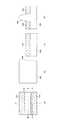
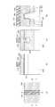
図1は、本発明の好ましい第1の実施形態による半導体装置の構造を説明するための模式的な斜視図である。また、図2は、図1に示す半導体装置の模式的な分解斜視図である。 FIG. 1 is a schematic perspective view for explaining the structure of a semiconductor device according to a preferred first embodiment of the present invention. FIG. 2 is a schematic exploded perspective view of the semiconductor device shown in FIG.
図1に示すように、本実施形態による半導体装置は、半導体基板10と、半導体基板10に形成されたトレンチ11と、トレンチ11の底部に設けられたSTI12とを有している。STI12は、トレンチ11の底部から途中まで埋め込んだ状態となっており、このSTI12よりも上に突出した半導体基板の一部であるフィン状の部分がフィン型活性領域13となっている。フィン型活性領域13は、図1に示すY方向に延在しており、上面13tと2つの側面13sを有している。フィン型活性領域13の側面13sは、STI12の側面と同一平面を構成している。 As shown in FIG. 1, the semiconductor device according to the present embodiment includes a
図1に示すように、フィン型活性領域13の側面13sはテーパーを有しており、このため、フィン型活性領域13の断面は台形状である。ここで、フィン型活性領域13の断面とは、図1に示すX方向に沿った切断面を指す。フィン型活性領域13がこのような形状を有しているのは、フィン型活性領域13とトレンチ11が同一工程で形成されたためである。つまり、STIへの絶縁膜の埋め込み性を向上させるためには、STI12の側面(=トレンチ11の側面)をテーパー状とする必要があり、フィン型活性領域13とトレンチ11を同一工程で形成すると、必然的に、フィン型活性領域13の側面13sもテーパー状となる。 As shown in FIG. 1, the
このように、フィン型活性領域13の断面は台形状であることから、フィン型活性領域13のX方向における幅は、上部ほど狭く、下部ほど広い。 Thus, since the cross section of the fin-type
また、本実施形態による半導体装置は、フィン型活性領域13と交差するようにX方向に延在するゲート電極14を有している。これにより、フィン型活性領域13の両側面13sの一部及び上面13tの一部は、ゲート電極14によって覆われている。後述するように、フィン型活性領域内には、ゲート電極14を挟んでソース領域15とドレイン領域16が形成されており、これによってフィントランジスタが構成されている。 In addition, the semiconductor device according to the present embodiment has the
図1に示すように、ゲート電極14のY方向における幅は、上部領域においてほぼ一定であるのに対し、下部領域においては半導体基板10に近くなるほど広がっている。より具体的に説明すると、ゲート電極14の内側面は、図2(b)に示すように、フィン型活性領域13の側面13sの一部を覆う側面被覆部14sと、上面13tの一部を覆う上面被覆部14tを備えている。図2(a)には、フィン型活性領域13の側面13s及び上面13tにおいて、ゲート電極14の側面被覆部14sと上面被覆部14tに対応する部分にハッチングを施してある。 As shown in FIG. 1, the width of the
側面被覆部14sは、Y方向における幅がほぼ一定な非テーパー部14s1と、上部から下部に向けてY方向における幅が広くなるテーパー部14s2とを有している。非テーパー部14s1のY方向における幅は、上面被覆部14tのY方向における幅と実質的に一致している。 The side
このように、非テーパー部14s1においては、フィン型活性領域13のX方向における幅に関わらずゲート電極14のY方向における幅は一定であるが、テーパー部14s2においては、フィン型活性領域13のX方向における幅が広くなるほど、ゲート電極14のY方向における幅も広くなっている。このため、下部においてはフィン型活性領域13のX方向における幅が大きいにも関わらず、これに応じてゲート電極14のY方向における幅も拡大されていることから、ゲート電極14による電界制御性が高められる。その結果、ソース領域15とドレイン領域16間のパンチスルーを抑制することが可能となる。 As described above, in the non-tapered portion 14s1, the width in the Y direction of the
しかも、フィン型活性領域13の上面13tにおいては、ゲート電極14は細く、すなわち、側面被覆部14sの上部と実質的に同じ幅となっているため、ゲート電極14の両側に形成されるソースコンタクト及びドレインコンタクト(図示省略)とゲート電極14とのショートマージンを広くとることができる。 In addition, since the
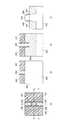
図3は、フィン型活性領域13をソース領域15、ドレイン領域16及びチャネル領域17に分解して示す分解斜視図であり、(a)は第1の例、(b)は第2の例である。 FIGS. 3A and 3B are exploded perspective views showing the fin-type
図3(a)に示す例は、チャネル領域111のY方向における幅、つまり、ソース領域15とドレイン領域16との距離が、フィン型活性領域13の上部から下部に亘ってほぼ一定である場合を示している。ソース領域15とドレイン領域16との距離は、ゲート電極14の上面被覆部14tの幅と実質的に一致している。このような構造は、ゲート電極14をマスクとして、半導体基板10に対して垂直な方向からイオン注入を行うことによって得られる。 In the example shown in FIG. 3A, the width of the channel region 111 in the Y direction, that is, the distance between the
図3(a)に示す構造である場合、フィン型活性領域13の下部におけるパンチスルーが生じやすい。しかしながら、本実施形態では、フィン型活性領域13の下部において、フィン型活性領域13のX方向における幅が広くなるほど、ゲート電極14のY方向における幅が拡大されていることから、このようなパンチスルーを防止することができる。 In the case of the structure shown in FIG. 3A, punch-through is likely to occur in the lower portion of the fin-type
一方、図3(b)に示す例は、チャネル領域111のY方向における幅、つまり、ソース領域15とドレイン領域16との距離が、ゲート電極14のY方向における幅と対応している場合を示している。つまり、ソース領域15とドレイン領域16との距離は、一部においてフィン型活性領域13の上部よりも下部の方が広くなっている。このような構造は、ゲート電極14をマスクとして、半導体基板10に対して斜め方向からイオン注入を行うことによって得られる。具体的には、フィン型活性領域13の一方の側面13sに対してイオン注入を行い、さらに、他方の側面13sに対してイオン注入を行えばよい。これにより、ソース領域15及びドレイン領域16の形状は、ゲート電極14の形状が反映された状態となる。 On the other hand, in the example shown in FIG. 3B, the width of the channel region 111 in the Y direction, that is, the distance between the
図3(b)に示す構造である場合、フィン型活性領域13の下部において、フィン型活性領域13のX方向における幅が広くなるほど、ソース領域15とドレイン領域16との距離が拡大されていることから、パンチスルーが生じにくくなる。これに加え、本実施形態では、フィン型活性領域13の下部において、フィン型活性領域13のX方向における幅が広くなるほど、ゲート電極14のY方向における幅が拡大されていることから、より効果的にパンチスルーを防止することが可能となる。 In the case of the structure shown in FIG. 3B, the distance between the
次に、本実施形態による半導体装置の製造方法につき、図4乃至図12を用いて説明する。図4乃至図12において、(a)は上面図を示し、(b)、(c)及び(d)は、それぞれ(a)に示すB−B線、C−C線及びD−D線に沿った断面図に対応している。また、D−D線が図1におけるX方向に対応し、B−B線及びC−C線が図1におけるY方向に対応している。 Next, the method for fabricating the semiconductor device according to the present embodiment will be explained with reference to FIGS. 4 to 12, (a) is a top view, and (b), (c), and (d) are respectively a BB line, a CC line, and a DD line shown in (a). Corresponds to a cross-sectional view along. Further, the DD line corresponds to the X direction in FIG. 1, and the BB line and the CC line correspond to the Y direction in FIG.
まず、図4に示すように、半導体基板100上のフィン型活性領域となる領域を覆うハードマスク101を形成する。ハードマスク101の材料としては、シリコン窒化膜を用いることが好ましい。 First, as shown in FIG. 4, a
続いて、図5に示すように、ハードマスク101を用いて、半導体基板100をエッチングし、例えば、深さ約250nmのトレンチ102を形成する。このトレンチ102はSTI用のトレンチであり、このため、垂直にエッチングするのではなく、所定のテーパーが形成されるようにエッチングする。このため、図5に示すように、半導体基板100のD−D線に沿った断面は台形状に加工される。 Subsequently, as shown in FIG. 5, the
次に、シリコン酸化膜を全面に形成し、その後、シリコン酸化膜の上部をウェットエッチングにより除去することにより、図6に示すように、トレンチ102の底部に、例えば、厚さ約100nmのSTI103を形成する。これにより、STI103から突き出した半導体基板100は、高さが例えば、約150nmのフィン型活性領域104となる。このフィン型活性領域104の断面形状は台形状である。 Next, a silicon oxide film is formed on the entire surface, and then the upper portion of the silicon oxide film is removed by wet etching, so that an
次に、図7に示すように、フィン型活性領域104の表面(上面及び両側面)にゲート絶縁膜105を形成する。 Next, as shown in FIG. 7, a
続いて、図8に示すように、全面にDOPOS(ドープドポリシリコン)膜106を形成し、続いてCMP(Chemical Mechanical Polishing)を行い、ゲート絶縁膜105上における厚さが約100nmとなるように平坦化する。 Subsequently, as shown in FIG. 8, a DOPOS (doped polysilicon)
次に、図9に示すように、DOPOS膜106上にゲート電極形成用の幅約100nmのシリコン窒化膜からなるハードマスク107を形成する。 Next, as shown in FIG. 9, a
次に、ハードマスク107を用いて、DOPOS膜106をドライエッチングによりゲート電極形状にパターニングするが、この工程は、以下のように2つのステップにより行う。 Next, the
まず、第1のステップでは、図10に示すようにHBrガス、O2ガス及びSF6ガスの混合ガスを用いて、少なくともフィン型活性領域104の表面が露出するまでDOPOS膜106を垂直にエッチングする。例えば、ゲート絶縁膜105上におけるDOPOS膜106の厚さが約100nmである場合、約150nmエッチングすればよい。これにより、DOPOS膜106のエッチングされずに残った部分の膜厚が約100nmとなる。First, in the first step, as shown in FIG. 10, the
次に、第2のステップでは、上記DOPOS膜106の残りの部分のエッチングを行う。この第2のステップにおけるドライエッチングにおいても、上記第1のステップで用いたガスと同じくHBrガス、O2ガス及びSF6ガスの混合ガスを用いる。しかし、第2のステップでは、O2ガスを第1のステップよりも約15〜35%増やしてドライエッチングを行う。このように、O2ガスを若干増加させることにより、図11に示すように、第2のステップでは、DOPOS膜106は垂直ではなく、テーパー形状にエッチングされる。Next, in the second step, the remaining portion of the
このように、第1及び第2のステップによってDOPOS膜106をエッチングすることにより、図11(c)に示すように、図2(b)に示す側面被覆部14sの非テーパー部14s1及びテーパー部14s2にほぼ対応する非テーパー部108s1及びテーパー部108s2を有するゲート電極108が形成される。 Thus, by etching the
次に、ゲート電極108をマスクとして、半導体基板100に対して垂直な方向からイオン注入を行うことにより、図12に示すように、ソース領域109及びドレイン領域110が形成され、フィントランジスタが完成する。 Next, by performing ion implantation from a direction perpendicular to the
このように、本実施形態による製造方法によれば、DOPOS膜106のパターニング時におけるエッチングガスを途中で切り替えるだけで、非テーパー部108s1及びテーパー部108s2を有するゲート電極108を形成することが可能となる。 As described above, according to the manufacturing method of the present embodiment, the
以下、本発明の好ましい第2の実施形態につき説明する。第2の実施形態は、上記第1の実施形態とは特にゲート電極の形状が異なった例である。 The second preferred embodiment of the present invention will be described below. The second embodiment is an example in which the shape of the gate electrode is particularly different from the first embodiment.
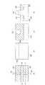
図13は、本発明の好ましい第2の実施形態による半導体装置の構造を説明するための模式的な斜視図である。 FIG. 13 is a schematic perspective view for explaining the structure of the semiconductor device according to the preferred second embodiment of the present invention.
図13に示すように、本実施形態による半導体装置は、半導体基板20と、半導体基板20に形成されたトレンチ21と、トレンチ21の底部に設けられたSTI22とを有している。STI22は、トレンチ21の底部から途中まで埋め込んだ状態となっている。 As shown in FIG. 13, the semiconductor device according to the present embodiment includes a
本実施形態では、上記第1の実施形態とは異なり、このSTI22よりも上に突出した半導体基板の一部であるフィン状の部分だけでなく、STI22の表面から図13中に二点鎖線で示す所定の深さまでの部分がフィン型活性領域23となっている。フィン型活性領域23は、図13に示すY方向に延在しており、上面23tと2つの側面23sを有している。フィン型活性領域23の側面23sは、STI22の側面と同一平面を構成している。 In the present embodiment, unlike the first embodiment, not only the fin-shaped portion that is a part of the semiconductor substrate protruding above the
図13に示すように、フィン型活性領域23の側面23sはテーパーを有しており、このため、フィン型活性領域23の断面は台形状である。ここで、フィン型活性領域23の断面とは、図13に示すX方向に沿った切断面を指す。フィン型活性領域23がこのような形状を有しているのは、上記第1の実施形態と同様、フィン型活性領域23とトレンチ21が同一工程で形成されたためである。 As shown in FIG. 13, the
このように、フィン型活性領域23の断面は台形状であることから、フィン型活性領域23のX方向における幅は、上部ほど狭く、下部ほど広い。 Thus, since the cross section of the fin-type
また、本実施形態による半導体装置は、フィン型活性領域23と交差するようにX方向に延在するゲート電極24を有している。これにより、フィン型活性領域23の両側面23sの一部及び上面23tの一部は、ゲート電極24によって覆われている。本実施形態においては、ゲート電極24の一部がSTI22に埋め込まれている。フィン型活性領域23内には、ゲート電極24を挟んでソース領域25とドレイン領域26が二点鎖線で示す深さまで形成されており、これによってフィントランジスタが構成されている。 In addition, the semiconductor device according to the present embodiment has the
図13に示すように、ゲート電極24のY方向における幅は、STI22よりも上部領域においてほぼ一定である。これに対し、STI22に埋め込まれたゲート電極24の下部領域は、Y方向における断面が楕円である楕円形状部24cを有している。より具体的に説明すると、ゲート電極24の内側面は、図13にハッチングを付して示すように、フィン型活性領域23の側面23sの一部を覆う側面被覆部24sと、上面23tの一部を覆う上面被覆部24tとを備えている。 As shown in FIG. 13, the width of the
そして、ゲート電極24の側面被覆部24sは、Y方向における幅がほぼ一定な直線部24s1と、楕円形状部24cのうちフィン型活性領域23と重なる半楕円形状部(楕円形状部24cの二点鎖線よりも上の部分)24s2とを有している。直線部24s1のY方向における幅は、上面被覆部24tのY方向における幅と実質的に一致している。なお、本発明において、「楕円形状」は「円形状」を含むものとする。 The side
このように、直線部24s1においては、フィン型活性領域23のX方向における幅に関わらずゲート電極24のY方向における幅は一定であるが、半楕円形状部24s2においては、フィン型活性領域23のX方向における幅が広くなるほど、ゲート電極24のY方向における幅も広くなっている。このため、下部においてはフィン型活性領域23のX方向における幅が大きいにも関わらず、これに応じてゲート電極24のY方向における幅も拡大されていることから、ゲート電極24による電界制御性が高められる。その結果、ソース領域25とドレイン領域26との間のパンチスルーを抑制することが可能となる。すなわち、本実施形態における半楕円形状部24s2が、上記第1の実施形態の図2における側面被覆部14sのテーパー部14s2と対応しており、したがって、第1の実施形態とほぼ同様の効果を得ることができる。 Thus, in the straight portion 24s1, the width in the Y direction of the
また、フィン型活性領域23の上面23tにおいては、ゲート電極24は細く、すなわち、側面被覆部24sの上部と実質的に同じ幅となっているため、ゲート電極24の両側に形成されるソースコンタクト及びドレインコンタクト(図示省略)とゲート電極24とのショートマージンを広くとることができる。 On the
本実施形態におけるソース領域25及びドレイン領域26の形成方法は、イオン注入の深さをSTI22の表面の高さまでではなく、図13に示すフィン型活性領域23の深さ(二点鎖線で示す)までとすること以外は、上記第1の実施形態について図3を用いて説明したものとほぼ同様であり、それによる効果もほぼ同様である。従って、ここではその説明を省略する。 In the method of forming the
次に、本発明の第2の実施形態による半導体装置の製造方法につき、図14乃至図25を用いて説明する。図14乃至図26において、(a)は上面図を示し、(b)、(c)及び(d)は、それぞれ(a)に示すB−B線、C−C線及びD−D線に沿った断面図に対応している。また、D−D線が図13におけるX方向に対応し、B−B線及びC−C線が図13におけるY方向に対応している。 Next, a semiconductor device manufacturing method according to the second embodiment of the present invention will be described with reference to FIGS. 14 to 26, (a) shows a top view, and (b), (c), and (d) show the BB line, CC line, and DD line shown in (a), respectively. Corresponds to a cross-sectional view along. Further, the DD line corresponds to the X direction in FIG. 13, and the BB line and the CC line correspond to the Y direction in FIG.
まず、図14に示すように、半導体基板200上のフィン型活性領域となる領域を覆うシリコン窒化膜からなるハードマスク201を形成する。 First, as shown in FIG. 14, a
続いて、図15に示すように、ハードマスク201を用いて、半導体基板200をエッチングし、例えば、深さ約250nmのトレンチ202を形成する。 Subsequently, as shown in FIG. 15, the
次に、シリコン酸化膜を全面に形成し、その後、シリコン酸化膜の上部をウェットエッチングにより除去することにより、図16に示すように、トレンチ202を埋め込み、表面が半導体基板200とほぼ同じ高さ、すなわち、厚さ約250nmのSTI203を形成する。 Next, a silicon oxide film is formed on the entire surface, and thereafter, the upper portion of the silicon oxide film is removed by wet etching, thereby filling the
次に、図17に示すように、STI203の延在方向と直行する方向に幅約100nmの開口を有する厚さ約120nmのシリコン窒化膜からなるハードマスク205を形成する。 Next, as shown in FIG. 17, a
次に、ハードマスク205を用いてシリコン酸化膜からなるSTI203を約100nmエッチングする。これにより、図18に示すように、フィン型活性領域204が形成される。 Next, the
続いて、全面に厚さ約20nmのシリコン窒化膜を形成し、その後エッチバックを行うことにより、図19に示すように、ハードマスク205の開口及びその下のSTI203に形成された開口の内側面及びフィン型活性領域204の側面にシリコン窒化膜からなる厚さ約20nmのサイドウォール206を形成する。 Subsequently, a silicon nitride film having a thickness of about 20 nm is formed on the entire surface, and then etched back, whereby the inner surface of the opening of the
次に、図20に示すように、ハードマスク205及びサイドウォール206をマスクとして、シリコン酸化膜からなるSTI203に対し、等方性エッチング(例えば、約50nm)を行う。これにより、図20(c)に示すように、断面が楕円形状の溝207が形成される。 Next, as shown in FIG. 20, isotropic etching (for example, about 50 nm) is performed on the
次に、図21に示すように、ハードマスク205及びサイドウォール206をエッチング除去する。 Next, as shown in FIG. 21, the
次に、図22に示すように、フィン型活性領域204の上面、及び溝207内に露出した側面上にゲート絶縁膜208を形成する。 Next, as shown in FIG. 22, a
続いて、図23に示すように溝207を埋め込むように、全面にDOPOS膜209を形成し、ゲート絶縁膜208上における厚さが約100nmとなるようにする。 Subsequently, as shown in FIG. 23, a
次に、図24に示すように、DOPOS膜209上にゲート電極形成用の例えば、幅約100nmのシリコン窒化膜からなるハードマスク210を形成する。 Next, as shown in FIG. 24, a
次に、図25に示すように、ハードマスク210を用いて、DOPOS膜209をドライエッチングによりゲート電極形状にパターニングする。こうして、ゲート電極211は、C−C線における断面が、楕円形状部211cと、その上部に楕円形状部211cの最大幅211cxよりも幅の狭い直線部211s1を備えた形状となる。 Next, as shown in FIG. 25, using the
続いて、ゲート電極211をマスクとして、半導体基板200に対して垂直な方向からイオン注入を行うことにより、図26に示すように、ソース領域212及びドレイン領域213が形成され、フィントランジスタが完成する。このとき、ソース領域212及びドレイン領域213の底部がゲート電極211の楕円形状部211cの幅がほぼ最大となる深さ(フィン型活性領域204の底部)とほぼ同じ深さとなるようにする。 Subsequently, by performing ion implantation from a direction perpendicular to the
このようにソース領域212及びドレイン領域213を形成することによって、フィン型活性領域204の側面においては、ゲート電極211の楕円形状部211cの上半分である半楕円形状部211s2とその上の直線部211s1によって電界制御されることとなる。すなわち、ゲート電極211は、図13に示す側面被覆部24sの直線部24s1に対応する直線部211s1と、半楕円形状部24s2に対応する半楕円形状部211s2を有する構成となる。 By forming the
このように、第2の実施形態によれば、第1の実施形態のように、エッチングガスの量を高精度に微調整するという困難なプロセスをともなうことなく、図13に示す構造の半導体装置を容易に形成することが可能である。 Thus, according to the second embodiment, unlike the first embodiment, the semiconductor device having the structure shown in FIG. 13 does not involve the difficult process of finely adjusting the amount of etching gas with high accuracy. Can be easily formed.
以上、本発明の好ましい実施の形態について説明したが、本発明は、上記の実施形態に限定されることなく、本発明の主旨を逸脱しない範囲で種々の変更が可能であり、それらも本発明の範囲内に包含されるものであることはいうまでもない。 The preferred embodiments of the present invention have been described above, but the present invention is not limited to the above-described embodiments, and various modifications can be made without departing from the spirit of the present invention. Needless to say, it is included in the range of.
上記実施の形態においては、ゲート電極がフィン型活性領域の側面を覆う部分(側面被覆部)の形状を上部が非テーパー形状で下部がテーパー形状であるもの及び上部が直線形状で下部が半楕円形状であるものにつき説明したが、これらの形状に限るものではない。例えば、非テーパー形状(又は直線形状)を有さずに、ゲート電極の上端部から下端部にかけてテーパー形状(台形状)であってもよい。あるいは上部が幅の狭い四角形状で、下部が幅の広い四角形状(凸型)等にしても構わない。 In the above embodiment, the part of the gate electrode covering the side surface of the fin-type active region (side covering part) has a non-tapered upper part and a tapered lower part, and the upper part is linear and the lower part is semi-elliptical. Although the description has been given of the shape, it is not limited to these shapes. For example, it may be a tapered shape (trapezoidal shape) from the upper end portion to the lower end portion of the gate electrode without having a non-tapered shape (or a straight line shape). Alternatively, the upper portion may be a narrow quadrangular shape, and the lower portion may be a wide quadrangular shape (convex shape).
上記実施形態による製造方法の説明においては、ソース及びドレイン領域をいずれも半導体基板に対して垂直な方向からイオン注入することにより形成する例を示しているが、これに代えて図3(b)に示したように半導体基板に対して斜め方向からイオン注入を行うことにより形成することももちろん可能である。 In the description of the manufacturing method according to the above embodiment, an example in which both the source and drain regions are formed by ion implantation from a direction perpendicular to the semiconductor substrate is shown, but instead of this, FIG. Of course, it is possible to form the semiconductor substrate by implanting ions from an oblique direction.
10,20,100,200 半導体基板
11,21,102,202 トレンチ
13,23,104,204 フィン型活性領域
13s,23s フィン型活性領域13の側面
13t,23t フィン型活性領域13の上面
14,24,108,211 ゲート電極
14s ゲート電極14の側面被覆部
14s1 側面被覆部14sの非テーパー部
14s2 側面被覆部14sのテーパー部
14t ゲート電極14の上面被覆部
15,25,109,212 ソース領域
16,26,110,213 ドレイン領域
17 チャネル領域
101,107,201,205,210 ハードマスク
105,208 ゲート絶縁膜
106,209 DOPOS膜
108s1 ゲート電極108の非テーパー部
108s2 ゲート電極108のテーパー部
24c ゲート電極24の楕円形状部
24s ゲート電極24の側面被覆部
24s1 側面被覆部24sの直線部
24s2 側面被覆部24sの半楕円形状部
24t ゲート電極24の上面被覆部
206 サイドウォール
207 溝
211c ゲート電極211の楕円形状部
211cx 楕円形状部211cの最大幅
211s1 ゲート電極211の直線部
211s2 ゲート電極211の半楕円形状部10, 20, 100, 200 Semiconductor substrate 11, 21, 102, 202 Trench 13, 23, 104, 204 Fin-type active region 13s, 23s Side surface 13t of fin-type active region 13, 23t Upper surface 14 of fin-type active region 13, 24, 108, 211 Gate electrode 14s Side surface covering portion 14s1 of gate electrode 14 Non-tapered portion 14s2 of side surface covering portion 14s Tapered portion 14t of side surface covering portion 14s Top surface covering portions 15, 25, 109, 212 of gate electrode 14 Source region 16 , 26, 110, 213 Drain region 17 Channel region 101, 107, 201, 205, 210 Hard mask 105, 208 Gate insulating film 106, 209 DOPOS film 108s1 Non-tapered portion 108s2 of gate electrode 108 Tapered portion 24c of gate electrode 108 Gate Electrode 2 4 oval shaped portion 24 s Side surface covering portion 24 s 1 of the gate electrode 24 Linear portion 24 s 2 of the side surface covering portion 24 s Semi-elliptical shape portion 24 t of the side surface covering portion 24 s Upper surface covering portion 206 of the gate electrode 24 Side wall 207 Groove 211 c Ellipse of the gate electrode 211 Shape portion 211cx Maximum width 211s1 of the elliptical portion 211c Linear portion 211s2 of the gate electrode 211 Semi-elliptical portion of the gate electrode 211
Claims (19)
Translated fromJapanese前記フィン型活性領域の前記側面の一部を覆う側面被覆部及び上面の一部を覆う上面被覆部を有するゲート電極と、
前記フィン型活性領域内に形成されたソース領域及びドレイン領域とを備え、
前記ゲート電極の前記側面被覆部の少なくとも一部は、上部よりも下部の方が幅が広いことを特徴とする半導体装置。A fin-type active region having tapered side surfaces;
A gate electrode having a side surface covering portion covering a part of the side surface of the fin-type active region and an upper surface covering portion covering a part of the upper surface;
A source region and a drain region formed in the fin-type active region,
At least a part of the side surface covering portion of the gate electrode is wider at the lower portion than at the upper portion.
前記フィン型活性領域の前記側面の一部を覆う側面被覆部及び上面の一部を覆う上面被覆部を有するゲート電極と、
前記フィン型活性領域内に形成されたソース領域及びドレイン領域とを備え、
前記ソース領域と前記ドレイン領域との距離は、少なくとも一部において前記フィン型活性領域の上部よりも下部の方が広いことを特徴とする半導体装置。A fin-type active region having tapered side surfaces;
A gate electrode having a side surface covering portion covering a part of the side surface of the fin-type active region and an upper surface covering portion covering a part of the upper surface;
A source region and a drain region formed in the fin-type active region,
The distance between the source region and the drain region is at least partly wider in the lower part than in the upper part of the fin-type active region.
前記フィン型活性領域の両側面の一部を覆う側面被覆部及び上面の一部を覆う上面被覆部を有するゲート電極を形成する工程と、
前記ゲート電極をマスクとして前記フィン型活性領域にイオン注入を行い、前記フィン型活性領域内にソース領域及びドレイン領域を形成する工程を備え、
前記ゲート電極は、前記側面被覆部の少なくとも一部が上部よりも下部の方が幅が広くなるように形成されることを特徴とする半導体装置の製造方法。Forming a fin-type active region having a tapered cross-section;
Forming a side electrode covering part of both side surfaces of the fin-type active region and a gate electrode having an upper surface covering part covering a part of the upper surface;
Ion implantation into the fin-type active region using the gate electrode as a mask, and forming a source region and a drain region in the fin-type active region,
The method of manufacturing a semiconductor device, wherein the gate electrode is formed such that at least a part of the side surface covering portion is wider in the lower part than in the upper part.
Priority Applications (2)
| Application Number | Priority Date | Filing Date | Title |
|---|---|---|---|
| JP2007141395AJP2008300384A (en) | 2007-05-29 | 2007-05-29 | Semiconductor device and manufacturing method thereof |
| US12/153,971US20080296667A1 (en) | 2007-05-29 | 2008-05-28 | Semiconductor device and manufacturing method thereof |
Applications Claiming Priority (1)
| Application Number | Priority Date | Filing Date | Title |
|---|---|---|---|
| JP2007141395AJP2008300384A (en) | 2007-05-29 | 2007-05-29 | Semiconductor device and manufacturing method thereof |
Publications (1)
| Publication Number | Publication Date |
|---|---|
| JP2008300384Atrue JP2008300384A (en) | 2008-12-11 |
Family
ID=40087149
Family Applications (1)
| Application Number | Title | Priority Date | Filing Date |
|---|---|---|---|
| JP2007141395AAbandonedJP2008300384A (en) | 2007-05-29 | 2007-05-29 | Semiconductor device and manufacturing method thereof |
Country Status (2)
| Country | Link |
|---|---|
| US (1) | US20080296667A1 (en) |
| JP (1) | JP2008300384A (en) |
Cited By (6)
| Publication number | Priority date | Publication date | Assignee | Title |
|---|---|---|---|---|
| JP2011243802A (en)* | 2010-05-19 | 2011-12-01 | Elpida Memory Inc | Semiconductor device, manufacturing method thereof, and data processing system |
| US8629512B2 (en) | 2012-03-28 | 2014-01-14 | Taiwan Semiconductor Manufacturing Company, Ltd. | Gate stack of fin field effect transistor with slanted sidewalls |
| KR20140088419A (en)* | 2013-01-02 | 2014-07-10 | 삼성전자주식회사 | Field effect transistor |
| KR101776411B1 (en)* | 2015-02-26 | 2017-09-07 | 타이완 세미콘덕터 매뉴팩쳐링 컴퍼니 리미티드 | Fin field effect transistor (finfet) device structure and method for forming the same |
| JP2017539098A (en)* | 2014-12-15 | 2017-12-28 | サン・ユー・キム | Fin-type field effect transistor |
| WO2019012839A1 (en)* | 2017-07-12 | 2019-01-17 | ソニーセミコンダクタソリューションズ株式会社 | Transistor and electronic device |
Families Citing this family (26)
| Publication number | Priority date | Publication date | Assignee | Title |
|---|---|---|---|---|
| JP2008098553A (en)* | 2006-10-16 | 2008-04-24 | Elpida Memory Inc | Semiconductor device and manufacturing method thereof |
| JP2011077185A (en)* | 2009-09-29 | 2011-04-14 | Elpida Memory Inc | Semiconductor device, method of manufacturing semiconductor device, and data processing system |
| CN103022100B (en)* | 2011-09-27 | 2015-09-02 | 中芯国际集成电路制造(上海)有限公司 | Structure of fin field effect pipe and forming method thereof |
| US20130193513A1 (en)* | 2012-02-01 | 2013-08-01 | International Business Machines Corporation | Multi-Gate Field Effect Transistor with a Tapered Gate Profile |
| KR101876793B1 (en)* | 2012-02-27 | 2018-07-11 | 삼성전자주식회사 | Field Effect Transistor and Method of fabricating the same |
| US8742509B2 (en)* | 2012-03-01 | 2014-06-03 | Taiwan Semiconductor Manufacturing Company, Ltd. | Apparatus and method for FinFETs |
| US9368388B2 (en)* | 2012-04-13 | 2016-06-14 | Taiwan Semiconductor Manufacturing Company, Ltd. | Apparatus for FinFETs |
| US9183977B2 (en)* | 2012-04-20 | 2015-11-10 | Infineon Technologies Ag | Method for fabricating a coil by way of a rounded trench |
| US9991375B2 (en) | 2012-05-30 | 2018-06-05 | Taiwan Semiconductor Manufacturing Company, Ltd. | Metal gate electrode of a semiconductor device |
| US9166053B2 (en) | 2013-02-22 | 2015-10-20 | Taiwan Semiconductor Manufacturing Company, Ltd. | FinFET device including a stepped profile structure |
| US9054044B2 (en) | 2013-03-07 | 2015-06-09 | Globalfoundries Inc. | Method for forming a semiconductor device and semiconductor device structures |
| US9041125B2 (en) | 2013-03-11 | 2015-05-26 | Taiwan Semiconductor Manufacturing Company, Ltd. | Fin shape for fin field-effect transistors and method of forming |
| US9991285B2 (en) | 2013-10-30 | 2018-06-05 | Taiwan Semiconductor Manufacturing Company, Ltd. | Mechanisms for forming FinFET device |
| US9583351B2 (en)* | 2013-11-19 | 2017-02-28 | Globalfoundries Inc. | Inverted contact |
| US20160049488A1 (en)* | 2014-08-13 | 2016-02-18 | Globalfoundries Inc. | Semiconductor gate with wide top or bottom |
| KR102287398B1 (en) | 2015-01-14 | 2021-08-06 | 삼성전자주식회사 | Semiconductor device |
| KR102327143B1 (en) | 2015-03-03 | 2021-11-16 | 삼성전자주식회사 | Integrated circuit device |
| KR102328564B1 (en) | 2015-04-14 | 2021-11-18 | 삼성전자주식회사 | Semiconductor devices and methods of manufacturing the same |
| CN106206302B (en)* | 2015-04-29 | 2019-09-27 | 中芯国际集成电路制造(上海)有限公司 | The forming method of fin formula field effect transistor |
| US10068980B1 (en) | 2017-04-26 | 2018-09-04 | International Business Machines Corporation | Vertical fin with a gate structure having a modified gate geometry |
| KR102303300B1 (en) | 2017-08-04 | 2021-09-16 | 삼성전자주식회사 | Semiconductor device |
| CN107481937B (en)* | 2017-08-21 | 2020-07-03 | 扬州江新电子有限公司 | Fin-type field effect transistor with double-angle trapezoidal cross-sectional shape and evaluation method thereof |
| CN111613583B (en) | 2019-02-25 | 2023-07-14 | 中芯国际集成电路制造(上海)有限公司 | Semiconductor device and method of forming the same |
| US11189697B2 (en) | 2020-04-01 | 2021-11-30 | Taiwan Semiconductor Manufacturing Co., Ltd. | Ultra-thin fin structure and method of fabricating the same |
| US11670675B2 (en)* | 2020-12-04 | 2023-06-06 | United Semiconductor Japan Co., Ltd. | Semiconductor device |
| US11705515B2 (en)* | 2021-03-05 | 2023-07-18 | Taiwan Semiconductor Manufacturing Company, Ltd. | Gate electrode extending into a shallow trench isolation structure in high voltage devices |
Family Cites Families (8)
| Publication number | Priority date | Publication date | Assignee | Title |
|---|---|---|---|---|
| US7045401B2 (en)* | 2003-06-23 | 2006-05-16 | Sharp Laboratories Of America, Inc. | Strained silicon finFET device |
| JP3962009B2 (en)* | 2003-12-05 | 2007-08-22 | 株式会社東芝 | Manufacturing method of semiconductor device |
| US7385247B2 (en)* | 2004-01-17 | 2008-06-10 | Samsung Electronics Co., Ltd. | At least penta-sided-channel type of FinFET transistor |
| US7332386B2 (en)* | 2004-03-23 | 2008-02-19 | Samsung Electronics Co., Ltd. | Methods of fabricating fin field transistors |
| JP4675585B2 (en)* | 2004-06-22 | 2011-04-27 | シャープ株式会社 | Field effect transistor |
| JP2006049627A (en)* | 2004-08-05 | 2006-02-16 | Toshiba Corp | Semiconductor device and manufacturing method thereof |
| US20060086977A1 (en)* | 2004-10-25 | 2006-04-27 | Uday Shah | Nonplanar device with thinned lower body portion and method of fabrication |
| US7547637B2 (en)* | 2005-06-21 | 2009-06-16 | Intel Corporation | Methods for patterning a semiconductor film |
- 2007
- 2007-05-29JPJP2007141395Apatent/JP2008300384A/ennot_activeAbandoned
- 2008
- 2008-05-28USUS12/153,971patent/US20080296667A1/ennot_activeAbandoned
Cited By (18)
| Publication number | Priority date | Publication date | Assignee | Title |
|---|---|---|---|---|
| JP2011243802A (en)* | 2010-05-19 | 2011-12-01 | Elpida Memory Inc | Semiconductor device, manufacturing method thereof, and data processing system |
| US10388767B2 (en) | 2012-03-28 | 2019-08-20 | Taiwan Semiconductor Manufacturing Company, Ltd. | Fin field effect transistor having angled fin sidewall |
| KR101372603B1 (en)* | 2012-03-28 | 2014-03-10 | 타이완 세미콘덕터 매뉴팩쳐링 컴퍼니 리미티드 | Gate stack of fin field effect transistor |
| US9196732B2 (en) | 2012-03-28 | 2015-11-24 | Taiwan Semiconductor Manufacturing Company, Ltd. | Fin field effect transistor having tapered sidewalls, and method of forming the same |
| US9825150B2 (en) | 2012-03-28 | 2017-11-21 | Taiwan Semiconductor Manufacturing Company, Ltd. | Method of forming fin field effect transistor having tapered sidewalls |
| US8629512B2 (en) | 2012-03-28 | 2014-01-14 | Taiwan Semiconductor Manufacturing Company, Ltd. | Gate stack of fin field effect transistor with slanted sidewalls |
| US11257930B2 (en) | 2012-03-28 | 2022-02-22 | Taiwan Semiconductor Manufaciuring Company, Ltd. | Method of forming fin field effect transistor |
| KR20140088419A (en)* | 2013-01-02 | 2014-07-10 | 삼성전자주식회사 | Field effect transistor |
| KR102017616B1 (en)* | 2013-01-02 | 2019-09-03 | 삼성전자주식회사 | Field effect transistor |
| JP2017539098A (en)* | 2014-12-15 | 2017-12-28 | サン・ユー・キム | Fin-type field effect transistor |
| US10490665B2 (en) | 2014-12-15 | 2019-11-26 | Sang U. Kim | FinFET transistor |
| US11908941B2 (en) | 2014-12-15 | 2024-02-20 | Samsung Electronics Co., Ltd. | FinFET transistor |
| US11211494B2 (en) | 2014-12-15 | 2021-12-28 | Samsung Electronics Co., Ltd. | FinFET transistor |
| KR101776411B1 (en)* | 2015-02-26 | 2017-09-07 | 타이완 세미콘덕터 매뉴팩쳐링 컴퍼니 리미티드 | Fin field effect transistor (finfet) device structure and method for forming the same |
| WO2019012839A1 (en)* | 2017-07-12 | 2019-01-17 | ソニーセミコンダクタソリューションズ株式会社 | Transistor and electronic device |
| JP7071359B2 (en) | 2017-07-12 | 2022-05-18 | ソニーセミコンダクタソリューションズ株式会社 | Transistors and electronic devices |
| US11476350B2 (en) | 2017-07-12 | 2022-10-18 | Sony Semiconductor Solutions Corporation | Transistor and electronic device |
| JPWO2019012839A1 (en)* | 2017-07-12 | 2020-05-07 | ソニーセミコンダクタソリューションズ株式会社 | Transistors and electronic devices |
Also Published As
| Publication number | Publication date |
|---|---|
| US20080296667A1 (en) | 2008-12-04 |
Similar Documents
| Publication | Publication Date | Title |
|---|---|---|
| JP2008300384A (en) | Semiconductor device and manufacturing method thereof | |
| KR100720238B1 (en) | Semiconductor element and manufacturing method thereof | |
| JP4638292B2 (en) | Semiconductor device having multi-channel Fin field effect transistor | |
| US7718493B2 (en) | Method for forming semiconductor device | |
| KR100739653B1 (en) | Fin field effect transistor and its manufacturing method | |
| KR100843711B1 (en) | Semiconductor device adopting transistor having recess channel region and manufacturing method thereof | |
| KR100763337B1 (en) | Semiconductor device having buried gate line and manufacturing method thereof | |
| US7709328B2 (en) | Semiconductor device and method for fabricating same | |
| US7955913B2 (en) | Method for manufacturing semiconductor device | |
| US8507349B2 (en) | Semiconductor device employing fin-type gate and method for manufacturing the same | |
| JP2008034785A (en) | Semiconductor device and manufacturing method thereof | |
| US7683437B2 (en) | Semiconductor device having fin field effect transistor and manufacturing method thereof | |
| CN100563028C (en) | Five-channel fin transistor and manufacturing method thereof | |
| JP2007184518A (en) | Method for forming fin-structure semiconductor device | |
| US11557656B2 (en) | Semiconductor device having a capping pattern on a gate electrode | |
| JP2008034427A (en) | Semiconductor device and manufacturing method thereof | |
| JP2009021503A (en) | Semiconductor device and manufacturing method thereof | |
| JP2007013080A (en) | Manufacturing method of semiconductor device | |
| KR100618904B1 (en) | Semiconductor device including FIFNFT and manufacturing method | |
| CN110867413A (en) | Forming method of single diffusion region cut off | |
| KR100854502B1 (en) | Semiconductor device adopting transistor having recess channel region and manufacturing method thereof | |
| JP2007027678A (en) | Semiconductor element transistor and method of forming the same | |
| KR20060128472A (en) | Morse transistor having recessed gate electrode and manufacturing method thereof | |
| KR100753051B1 (en) | Saddle Pin Transistor Manufacturing Method | |
| JP2013110256A (en) | Semiconductor device manufacturing method |
Legal Events
| Date | Code | Title | Description |
|---|---|---|---|
| A621 | Written request for application examination | Free format text:JAPANESE INTERMEDIATE CODE: A621 Effective date:20100312 | |
| A762 | Written abandonment of application | Free format text:JAPANESE INTERMEDIATE CODE: A762 Effective date:20100930 |