JP2008280206A - Single crystal growth equipment - Google Patents
Single crystal growth equipmentDownload PDFInfo
- Publication number
- JP2008280206A JP2008280206AJP2007125336AJP2007125336AJP2008280206AJP 2008280206 AJP2008280206 AJP 2008280206AJP 2007125336 AJP2007125336 AJP 2007125336AJP 2007125336 AJP2007125336 AJP 2007125336AJP 2008280206 AJP2008280206 AJP 2008280206A
- Authority
- JP
- Japan
- Prior art keywords
- seed crystal
- single crystal
- gas guide
- raw material
- crystal
- Prior art date
- Legal status (The legal status is an assumption and is not a legal conclusion. Google has not performed a legal analysis and makes no representation as to the accuracy of the status listed.)
- Pending
Links
Images


Landscapes
- Crystals, And After-Treatments Of Crystals (AREA)
Abstract
Description
Translated fromJapanese本発明は、炭化珪素単結晶の製造装置及び単結晶の成長方法に関するものであり、特に単結晶の成長速度の再現性を向上させる技術に関する。 The present invention relates to a silicon carbide single crystal manufacturing apparatus and a single crystal growth method, and more particularly to a technique for improving the reproducibility of the growth rate of a single crystal.
従来、炭化珪素単結晶の製造方法としては昇華法(改良レーリー法)が広く用いられている。図5に昇華法に用いられる装置の概略図を示す。原料4として炭化珪素粉末が収容してある坩堝2と、種結晶支持部5を備えた坩堝蓋部1より構成されており、種結晶3は、種結晶支持部に原料4に対向するように配置されている。この種結晶3としては炭化珪素単結晶が用いられる。この状態で、原料4側が高温に、種結晶3側が低温になるように加熱され、原料4の昇華ガスが低温の種結晶3上で再結晶化することにより炭化珪素単結晶10が成長する。ところが、種結晶支持部5以外の坩堝蓋部1にも炭化珪素の結晶6が成長するため、種結晶3上の炭化珪素単結晶10の成長効率が低くなる。 Conventionally, a sublimation method (modified Rayleigh method) has been widely used as a method for producing a silicon carbide single crystal. FIG. 5 shows a schematic diagram of an apparatus used for the sublimation method. The
炭化珪素単結晶10を効率良く成長させるために、図6に示すように原料4と種結晶3との間に筒状(コーン状)ガスガイド部9を設ける方法が用いられている(例えば、特許文献1を参照。)。ガスガイド部9により昇華ガスを種結晶3に導くことができ、またガスガイド部9の種結晶3側端と種結晶支持部9および種結晶3との間に隙間を設けて昇華ガスの一部を坩堝蓋部1側へ流し、炭化珪素単結晶10をガスガイド部9に接触させずに成長させ、単結晶に応力が加わるのを防いで高品質な炭化珪素単結晶10を得ることが出来る。
しかしながら、前記従来のガスガイド部9を用いて炭化珪素単結晶10を成長させると、全く同じ条件で成長を行っても、炭化珪素単結晶10の成長速度に大きなバラツキが生じるという課題を有していた。 However, when the silicon carbide
本発明は、上記課題を解決するためになされたものであり、炭化珪素単結晶の結晶成長速度のバラツキを抑えるための単結晶成長装置を提供するものである。 The present invention has been made to solve the above-described problems, and provides a single crystal growth apparatus for suppressing variations in the crystal growth rate of a silicon carbide single crystal.
前記課題を解決するために、本発明の単結晶成長装置は、坩堝内に収容された単結晶成長用の原料を加熱して昇華させて種結晶上に供給し、炭化珪素単結晶を成長させる単結晶成長装置において、前記坩堝の前記原料に対向する位置に配置された前記種結晶を支持する円柱状の種結晶支持部と、前記原料と前記種結晶支持部との間に先細の中空ガスガイド部を設け、前記ガスガイド部の前記種結晶側端の開口部は、その反対端の開口部より小さく、且つ前記種結晶支持部を包むように配置された中空円筒部を有することを特徴としたものである。 In order to solve the above-mentioned problems, the single crystal growth apparatus of the present invention heats and sublimates a raw material for single crystal growth accommodated in a crucible and supplies it on a seed crystal to grow a silicon carbide single crystal. In the single crystal growth apparatus, a cylindrical seed crystal support portion that supports the seed crystal disposed at a position facing the raw material of the crucible, and a tapered hollow gas between the raw material and the seed crystal support portion A guide portion is provided, and the opening at the seed crystal side end of the gas guide portion is smaller than the opening at the opposite end, and has a hollow cylindrical portion arranged so as to wrap the seed crystal support portion. It is a thing.
本発明の単結晶成長装置及び単結晶成長方法によれば、同一の成長条件で結晶成長を行った際、炭化珪素単結晶の成長速度のバラツキを抑えることができる。 According to the single crystal growth apparatus and the single crystal growth method of the present invention, variation in the growth rate of the silicon carbide single crystal can be suppressed when crystal growth is performed under the same growth conditions.
以下に、本発明を用いた単結晶の成長装置及び成長方法の実施の形態を図面とともに詳細に説明する。また、単結晶として炭化珪素を用いて説明するが、他の単結晶の成長にも適用できるものである。 Embodiments of a single crystal growth apparatus and growth method using the present invention will be described below in detail with reference to the drawings. Further, although silicon carbide is used as the single crystal, the present invention can be applied to the growth of other single crystals.
(実施の形態1)
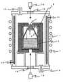
図1は、本発明で用いた成長装置の概略図である。坩堝2内に原料4として炭化珪素粉末を収容し、坩堝蓋部1の種結晶支持部5に固定した種結晶3を、原料4に対向するように配置した。種結晶3としては、4H型の炭化珪素単結晶を用い、結晶成長面は、(000−1)面とした。また、種結晶支持部5の種結晶貼付け面は、直径40mmの円形であり、種結晶3も同じく直径40mmの円形とした。原料4と種結晶3の間には、原料4から昇華したガスを種結晶3に効率良く導くために、原料4側が種結晶3側より大径の先細りの筒状をしたガスガイド部9を配置している。このガスガイド部9の種結晶3側は、種結晶支持部5および種結晶3に接触しておらず隙間を設けてある。原料4からの昇華ガスの一部が、この隙間を通って坩堝蓋部1側に流れることにより、成長する炭化珪素単結晶10がガスガイド部9に接触して応力を受け、転位やクラック等の欠陥が発生するのを防いでいる。(Embodiment 1)
FIG. 1 is a schematic view of a growth apparatus used in the present invention. A silicon carbide powder was housed in the
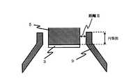
図2に本発明のガスガイド部9の詳細を示す。ガスガイド部9の種結晶3側端は、種結晶支持部5側面と平行に沿うような中空円筒部を形成しており、この中空円筒部の内壁と種結晶支持部5との間は距離Eを隔てて対抗している。ガスガイド部9の材料は坩堝と同様の材料である黒鉛を用いた。中空円筒部は坩堝蓋部1には接触しない高さとし、また、中空円筒部の内壁と種結晶支持部5との隙間の距離は1mmとした。ガスガイド部9の中空円筒部内壁と種結晶支持部5とが平行している距離は、後述の実施例1から3で示すように、1から3mmまで変化させて、炭化珪素単結晶の成長速度に及ぼす影響を観察した。 FIG. 2 shows details of the
坩堝2および坩堝蓋部1を断熱材8で覆った。これは、昇華法を用いた炭化珪素単結晶成長では、原料4を昇華させるために2000℃以上の高温が必要であるが、2000℃以上の高温では、温度の4乗に比例して輻射熱が失われるのを防ぐ目的である。この断熱材8で覆った坩堝2及び坩堝蓋部1を、石英製の反応管11内に配置した。この反応管11は、二重管構造になっており、結晶成長中には、冷却水12を流して冷却している。また反応管11の上部にガス導入口13が、下部にはガス排気口14が設けられている。 The
以上のように単結晶成長装置を組み立てて、次のプロセスで炭化珪素の結晶の成長を行った。まず、反応管11内部を不活性ガスで置換した。不活性ガスは、コスト、純度などの面から、アルゴン(Ar)が適している。この不活性ガス置換は、まずガス排気口14から反応管11内を高真空排気し、その後、ガス導入口13から不活性ガスを常圧まで充填した。然る後、アルゴンガスと共に、窒素ガスをガス導入口13から導入し、反応管11内が、後述の結晶成長時の圧力の時に、所望の窒素分圧になるように、アルゴンおよび窒素ガスの流量を調整した。本実施の形態では、具体的には、成長時の窒素分圧が33Paとなるように、アルゴンおよび窒素ガス流量を調整した。その後、反応管11の周囲に螺旋状に巻かれたコイル7に高周波電流を流すことにより、坩堝2および坩堝蓋部1を誘導加熱し昇温した。 A single crystal growth apparatus was assembled as described above, and silicon carbide crystals were grown by the following process. First, the inside of the reaction tube 11 was replaced with an inert gas. As the inert gas, argon (Ar) is suitable in terms of cost, purity, and the like. In this inert gas replacement, first, the inside of the reaction tube 11 was evacuated to a high vacuum from the
加熱時は、反応管11上下部に設けられている石英製の温度測定用窓15、及び断熱材8の上下部に設けられた温度測定用の穴を通して、放射温度計16で、坩堝2下部、及び坩堝蓋部1上部の温度を測定している。本実施の形態では、このうち坩堝蓋部1上部の温度を高周波電源(図示せず)にフィードバックし、コイル7に流す高周波電流を制御して温度制御を行っている。その時の坩堝2の下部温度は、坩堝蓋部1および坩堝2と、コイル7の相対位置により決まる。本実施の形態では、坩堝蓋部1上部温度を2200℃にし、坩堝2下部温度が2280℃となるように坩堝蓋部1および坩堝2とコイル7の相対位置を調整した。 At the time of heating, the
昇温時には、反応管11内部は、数10kPa程度の圧力にしておく必要がある。これは、低温時(所望の結晶成長温度以下)における原料4の昇華を防ぎ、結晶成長を開始させないようにするためである。このようにして、所望の温度まで昇温した後、徐々に圧力を下げて結晶成長を開始させる。本実施の形態では、反応管11内部の圧力を0.665kPaにし、80時間保持して結晶成長を行った。結晶成長終了時は、成長開始時とは逆に、反応管11内部の圧力を80kPaまで1時間かけて昇圧して原料4の昇華を止め、その後、常温までゆっくりと冷却した。 When raising the temperature, the inside of the reaction tube 11 needs to be kept at a pressure of about several tens of kPa. This is to prevent sublimation of the
以上のように構成した単結晶成長装置と結晶成長条件のプロセスとを用いて、次に述べる実施例1から3および比較例について炭化珪素の結晶成長を行った。 Using the single crystal growth apparatus configured as described above and the process of crystal growth conditions, silicon carbide crystals were grown for Examples 1 to 3 and Comparative Examples described below.
(実施例1)
ガスガイド部9の中空円筒部内壁と種結晶支持部5とが平行している距離を1mmとし、同一成長条件で5回の結晶成長を行った。Example 1
The distance at which the inner wall of the hollow cylindrical portion of the
(実施例2)
ガスガイド部9の中空円筒部内壁と種結晶支持部5とが平行している距離を2mmとし、同一成長条件で5回の結晶成長を行った。(Example 2)
The distance at which the inner wall of the hollow cylindrical portion of the
(実施例3)
ガスガイド部9の中空円筒部内壁5と種結晶支持部とが平行している距離を3mmとし、同一成長条件で5回の結晶成長を行った。(Example 3)
The distance in which the hollow cylindrical
(比較例)
ガスガイド部9の種結晶3側端の先端形状は尖っており、その先端は、種結晶3よりも1mmだけ坩堝蓋部1側に配置した。そして、同一成長条件で5回の結晶成長を行った。(Comparative example)
The tip shape of the end of the
図3に、実施例1から3及び比較例で結晶成長を行った結果を示す。いずれの場合も炭化珪素単結晶10は、ガスガイド部9に接触せず成長していたが、比較例と実施例1では、同一成長条件にも拘わらず、炭化珪素単結晶10の成長速度のバラツキが大きく、それぞれ23.6%、21.1%であった。一方、実施例2と実施例3の炭化珪素単結晶10の成長速度のバラツキは、それぞれ2.6%、2.8%であり、バラツキは非常に小さかった。従って、中空円筒内壁と種結晶支持部5との距離が2mmより小さいと、成長する炭化珪素単結晶10の成長速度のバラツキが大きいが、平行に沿っている距離が2mm以上の時は、炭化珪素単結晶10の成長速度のバラツキを抑制できる。 FIG. 3 shows the results of crystal growth in Examples 1 to 3 and the comparative example. In any case, the silicon carbide
図4を用いて、この成長速度のバラツキの差の原因を説明する。図4(a)は、中空円筒部が無く、先端形状が尖ったガスガイド部9であり、図4(b)は、中空円筒部内壁と種結晶支持部5とが平行している距離が2mm未満のガスガイド部9である。図3(a)および図3(b)に示すように、結晶成長時の高温且つ減圧環境により、黒鉛製のガスガイド部9の角部が劣化し、成長後には、ガスガイド部9の先端部は、変形しており、ガスガイド部9と種結晶支持部5との距離が広がっていた。また、この劣化具合は、同成長条件で結晶成長を行っても、成長毎に異なっていた。 The cause of the difference in the growth rate variation will be described with reference to FIG. FIG. 4A shows a
結晶成長時に原料4から昇華したガスは、ガスガイド部9により種結晶3に導かれるが、この昇華ガスの一部は、ガスガイド部9の種結晶3側端と種結晶支持部5との間の隙間から、坩堝蓋部1側へ流れる。これにより炭化珪素単結晶10をガスガイド部9に接触させずに成長させ、単結晶に応力が加わるのを防いで高品質な炭化珪素単結晶10を得ることができる。この際、ガスガイド部9の種結晶3側端と種結晶支持部5との間の隙間の距離が、昇華ガスの内、単結晶の成長に寄与する昇華ガスと坩堝蓋部1側に流れる昇華ガスの割合を決定している。 The gas sublimated from the
従って、ガスガイド部9の種結晶側先端部に中空円筒部が無いか、あるいは中空円筒部の高さが2mmより小さいと、図3(a)および図3(b)に示したように、結晶成長中にガスガイド部9の先端が劣化して、ガスガイド部9と種結晶支持部5との距離が変化することにより、単結晶の成長速度の大きなバラツキが生じる。 Therefore, if there is no hollow cylindrical part at the seed crystal side tip of the
また、ガスガイド部9の円筒部内壁と種結晶支持部5との距離は、0.5mm以上、3mm以下であることが望ましい。既述したように、ガスガイド部9の円筒部内壁と種結晶支持部5との隙間の距離により、炭化珪素単結晶の成長に寄与する昇華ガスと坩堝蓋部1側に流れる昇華ガスの割合を決定している。ガスガイド部9の円筒部内壁と種結晶支持部5との距離が0.5mmより短いと、種結晶3外周部から成長する炭化珪素単結晶10、あるいは坩堝蓋体1の種結晶支持部側壁面から成長する炭化珪素多結晶6により、この隙間が塞がれてしまう場合がある。また、ガスガイド部9の円筒部内壁と種結晶支持部5との距離が3mmより大きいと、原料4の昇華ガスのうち、坩堝蓋体1下面へ向かう昇華ガスの割合が非常に多くなり、炭化珪素単結晶10の成長に寄与する昇華ガスの割合が少なくなる。そのため、炭化珪素単結晶10の成長速度が著しく遅くなってしまう。 The distance between the cylindrical inner wall of the
更には、坩堝蓋部1下面からの炭化珪素多結晶6の伸長速度が大きくなるため、数10時間の結晶成長を行うと、坩堝蓋部1下面から伸長する炭化珪素多結晶6が、坩堝蓋体1の種結晶支持部5の高さより高くなり、種結晶3から成長する炭化珪素単結晶10と接触して炭化珪素単結晶10に歪を与え、転位やクラック等の欠陥が発生して結晶品質を悪化させる。従って、ガスガイド部9と種結晶支持部5が平行に沿っている部分の、ガスガイド部9の円筒部内壁と種結晶支持部5との距離は、0.5mm以上、3mm以下であることが望ましい。 Furthermore, since the growth rate of the
本発明にかかる単結晶の成長装置及び成長方法は、成長速度が速く、且つ高品質な単結晶を得ることができるため、昇華法により成長できる単結晶である硫化カドミウム(CdS)、セレン化カドミウム(CdSe)、硫化亜鉛(ZnS)、窒化アルミニウム(AlN)、窒化ホウ素(BN)などにも適用できる。 The apparatus and method for growing a single crystal according to the present invention has a high growth rate and can obtain a high-quality single crystal. Therefore, cadmium sulfide (CdS) and cadmium selenide, which are single crystals that can be grown by a sublimation method. It can also be applied to (CdSe), zinc sulfide (ZnS), aluminum nitride (AlN), boron nitride (BN), and the like.
1 坩堝蓋部
2 坩堝
3 種結晶
4 原料
5 種結晶支持部
6 炭化珪素多結晶
7 コイル
8 断熱材
9 ガスガイド部
10 炭化珪素単結晶
11 反応管
12 冷却水
13 ガス導入口
14 ガス排気口
15 温度測定用窓
16 放射温度計DESCRIPTION OF
Claims (4)
Translated fromJapanese前記坩堝の前記原料に対向する位置に配置された前記種結晶を支持する円柱状の種結晶支持部と、
前記原料と前記種結晶支持部との間に先細の中空ガスガイド部を設け、
前記ガスガイド部の前記種結晶側端の開口部は、その反対端の開口部より小さく、且つ前記種結晶支持部を包むように配置された中空円筒部を有する単結晶成長装置。In a single crystal growth apparatus for growing a single crystal by heating and sublimating a raw material for single crystal growth contained in a crucible and supplying it on a seed crystal,
A columnar seed crystal support part that supports the seed crystal disposed at a position facing the raw material of the crucible;
A tapered hollow gas guide part is provided between the raw material and the seed crystal support part,
An opening at the seed crystal side end of the gas guide part is smaller than an opening at the opposite end, and has a hollow cylindrical part arranged so as to wrap the seed crystal support part.
Priority Applications (1)
| Application Number | Priority Date | Filing Date | Title |
|---|---|---|---|
| JP2007125336AJP2008280206A (en) | 2007-05-10 | 2007-05-10 | Single crystal growth equipment |
Applications Claiming Priority (1)
| Application Number | Priority Date | Filing Date | Title |
|---|---|---|---|
| JP2007125336AJP2008280206A (en) | 2007-05-10 | 2007-05-10 | Single crystal growth equipment |
Publications (1)
| Publication Number | Publication Date |
|---|---|
| JP2008280206Atrue JP2008280206A (en) | 2008-11-20 |
Family
ID=40141336
Family Applications (1)
| Application Number | Title | Priority Date | Filing Date |
|---|---|---|---|
| JP2007125336APendingJP2008280206A (en) | 2007-05-10 | 2007-05-10 | Single crystal growth equipment |
Country Status (1)
| Country | Link |
|---|---|
| JP (1) | JP2008280206A (en) |
Cited By (4)
| Publication number | Priority date | Publication date | Assignee | Title |
|---|---|---|---|---|
| JP2014024703A (en)* | 2012-07-26 | 2014-02-06 | Sumitomo Electric Ind Ltd | Method of producing silicon carbide single crystal |
| JP2016011215A (en)* | 2014-06-27 | 2016-01-21 | 三菱電機株式会社 | Manufacturing apparatus and manufacturing method for single crystal |
| CN110050091A (en)* | 2016-12-26 | 2019-07-23 | 昭和电工株式会社 | The manufacturing method of single-crystal silicon carbide |
| KR20200075954A (en)* | 2018-12-18 | 2020-06-29 | 주식회사 포스코 | Growth device for silicon carbide single crystal |
Citations (4)
| Publication number | Priority date | Publication date | Assignee | Title |
|---|---|---|---|---|
| JP2002060297A (en)* | 2000-08-21 | 2002-02-26 | Agency Of Ind Science & Technol | Apparatus and method for growing single crystal |
| JP2005053739A (en)* | 2003-08-04 | 2005-03-03 | Denso Corp | Single crystal growth method and growth apparatus |
| JP2005225710A (en)* | 2004-02-12 | 2005-08-25 | Denso Corp | SiC single crystal manufacturing method and SiC single crystal manufacturing apparatus |
| JP2007077017A (en)* | 2006-10-19 | 2007-03-29 | National Institute Of Advanced Industrial & Technology | Single crystal growth apparatus and growth method |
- 2007
- 2007-05-10JPJP2007125336Apatent/JP2008280206A/enactivePending
Patent Citations (4)
| Publication number | Priority date | Publication date | Assignee | Title |
|---|---|---|---|---|
| JP2002060297A (en)* | 2000-08-21 | 2002-02-26 | Agency Of Ind Science & Technol | Apparatus and method for growing single crystal |
| JP2005053739A (en)* | 2003-08-04 | 2005-03-03 | Denso Corp | Single crystal growth method and growth apparatus |
| JP2005225710A (en)* | 2004-02-12 | 2005-08-25 | Denso Corp | SiC single crystal manufacturing method and SiC single crystal manufacturing apparatus |
| JP2007077017A (en)* | 2006-10-19 | 2007-03-29 | National Institute Of Advanced Industrial & Technology | Single crystal growth apparatus and growth method |
Cited By (7)
| Publication number | Priority date | Publication date | Assignee | Title |
|---|---|---|---|---|
| JP2014024703A (en)* | 2012-07-26 | 2014-02-06 | Sumitomo Electric Ind Ltd | Method of producing silicon carbide single crystal |
| JP2016011215A (en)* | 2014-06-27 | 2016-01-21 | 三菱電機株式会社 | Manufacturing apparatus and manufacturing method for single crystal |
| CN110050091A (en)* | 2016-12-26 | 2019-07-23 | 昭和电工株式会社 | The manufacturing method of single-crystal silicon carbide |
| CN110050091B (en)* | 2016-12-26 | 2021-03-05 | 昭和电工株式会社 | Method for producing silicon carbide single crystal |
| US11078598B2 (en) | 2016-12-26 | 2021-08-03 | Showa Denko K.K. | Method for producing silicon carbide single crystal |
| KR20200075954A (en)* | 2018-12-18 | 2020-06-29 | 주식회사 포스코 | Growth device for silicon carbide single crystal |
| KR102202447B1 (en)* | 2018-12-18 | 2021-01-14 | 주식회사 포스코 | Growth device for silicon carbide single crystal |
Similar Documents
| Publication | Publication Date | Title |
|---|---|---|
| JP4388538B2 (en) | Silicon carbide single crystal manufacturing equipment | |
| JP4547031B2 (en) | Crucible for producing silicon carbide single crystal, and apparatus and method for producing silicon carbide single crystal | |
| JP2007204309A (en) | Single crystal growth apparatus and single crystal growth method | |
| CN107208310B (en) | Manufacturing method of silicon carbide single crystal | |
| JP5560862B2 (en) | Silicon carbide single crystal ingot manufacturing equipment | |
| JP3491402B2 (en) | Single crystal manufacturing method and single crystal manufacturing apparatus | |
| JP6813779B2 (en) | Single crystal manufacturing equipment and single crystal manufacturing method | |
| JP6338439B2 (en) | Method for producing silicon carbide single crystal ingot | |
| KR101744287B1 (en) | Growth device for silicon carbide single crystal | |
| JP2004099340A (en) | Seed crystal for growing silicon carbide single crystal, silicon carbide single crystal ingot, and method for producing same | |
| CN116446046A (en) | Device and method for growing silicon carbide crystal by heat exchange physical vapor transport method | |
| JP5602093B2 (en) | Single crystal manufacturing method and manufacturing apparatus | |
| JP5614387B2 (en) | Silicon carbide single crystal manufacturing method and silicon carbide single crystal ingot | |
| JP4238450B2 (en) | Method and apparatus for producing silicon carbide single crystal | |
| JP2008115033A (en) | Graphite crucible for silicon carbide single crystal growth and silicon carbide single crystal manufacturing apparatus | |
| JP2007308355A (en) | Apparatus and method for manufacturing silicon carbide single crystal | |
| JP2008280206A (en) | Single crystal growth equipment | |
| JP5143139B2 (en) | Single crystal growth equipment | |
| JP2017065969A (en) | Graphite crucible for producing silicon carbide single crystal ingot and method for producing silicon carbide single crystal ingot | |
| EP3026146A1 (en) | METHOD FOR PRODUCING SiC SUBSTRATES | |
| JP5392040B2 (en) | Single crystal manufacturing apparatus and single crystal manufacturing method | |
| JP3491430B2 (en) | Single crystal manufacturing equipment | |
| WO2010050362A1 (en) | Method for manufacturing silicon carbide single crystal | |
| JP2017154953A (en) | Silicon carbide single crystal manufacturing equipment | |
| JP5428706B2 (en) | Method for producing SiC single crystal |
Legal Events
| Date | Code | Title | Description |
|---|---|---|---|
| A621 | Written request for application examination | Free format text:JAPANESE INTERMEDIATE CODE: A621 Effective date:20100216 | |
| RD01 | Notification of change of attorney | Free format text:JAPANESE INTERMEDIATE CODE: A7421 Effective date:20100312 | |
| A977 | Report on retrieval | Free format text:JAPANESE INTERMEDIATE CODE: A971007 Effective date:20110719 | |
| A131 | Notification of reasons for refusal | Free format text:JAPANESE INTERMEDIATE CODE: A131 Effective date:20110726 | |
| A521 | Request for written amendment filed | Free format text:JAPANESE INTERMEDIATE CODE: A523 Effective date:20110809 | |
| A131 | Notification of reasons for refusal | Free format text:JAPANESE INTERMEDIATE CODE: A131 Effective date:20110830 | |
| A02 | Decision of refusal | Free format text:JAPANESE INTERMEDIATE CODE: A02 Effective date:20120417 |