JP2008262616A - Semiconductor memory device, internal refresh stop method, contention processing method between external access and internal refresh, counter initialization method, external refresh refresh address detection method, and external refresh execution selection method - Google Patents
Semiconductor memory device, internal refresh stop method, contention processing method between external access and internal refresh, counter initialization method, external refresh refresh address detection method, and external refresh execution selection methodDownload PDFInfo
- Publication number
- JP2008262616A JP2008262616AJP2007102910AJP2007102910AJP2008262616AJP 2008262616 AJP2008262616 AJP 2008262616AJP 2007102910 AJP2007102910 AJP 2007102910AJP 2007102910 AJP2007102910 AJP 2007102910AJP 2008262616 AJP2008262616 AJP 2008262616A
- Authority
- JP
- Japan
- Prior art keywords
- refresh
- memory device
- counter
- semiconductor memory
- block
- Prior art date
- Legal status (The legal status is an assumption and is not a legal conclusion. Google has not performed a legal analysis and makes no representation as to the accuracy of the status listed.)
- Pending
Links
Images


Classifications
- G—PHYSICS
- G11—INFORMATION STORAGE
- G11C—STATIC STORES
- G11C11/00—Digital stores characterised by the use of particular electric or magnetic storage elements; Storage elements therefor
- G11C11/21—Digital stores characterised by the use of particular electric or magnetic storage elements; Storage elements therefor using electric elements
- G11C11/34—Digital stores characterised by the use of particular electric or magnetic storage elements; Storage elements therefor using electric elements using semiconductor devices
- G11C11/40—Digital stores characterised by the use of particular electric or magnetic storage elements; Storage elements therefor using electric elements using semiconductor devices using transistors
- G11C11/401—Digital stores characterised by the use of particular electric or magnetic storage elements; Storage elements therefor using electric elements using semiconductor devices using transistors forming cells needing refreshing or charge regeneration, i.e. dynamic cells
- G11C11/406—Management or control of the refreshing or charge-regeneration cycles
- G11C11/40603—Arbitration, priority and concurrent access to memory cells for read/write or refresh operations
- G—PHYSICS
- G11—INFORMATION STORAGE
- G11C—STATIC STORES
- G11C11/00—Digital stores characterised by the use of particular electric or magnetic storage elements; Storage elements therefor
- G11C11/21—Digital stores characterised by the use of particular electric or magnetic storage elements; Storage elements therefor using electric elements
- G11C11/34—Digital stores characterised by the use of particular electric or magnetic storage elements; Storage elements therefor using electric elements using semiconductor devices
- G11C11/40—Digital stores characterised by the use of particular electric or magnetic storage elements; Storage elements therefor using electric elements using semiconductor devices using transistors
- G11C11/401—Digital stores characterised by the use of particular electric or magnetic storage elements; Storage elements therefor using electric elements using semiconductor devices using transistors forming cells needing refreshing or charge regeneration, i.e. dynamic cells
- G11C11/406—Management or control of the refreshing or charge-regeneration cycles
- G11C11/40618—Refresh operations over multiple banks or interleaving
Landscapes
- Engineering & Computer Science (AREA)
- Microelectronics & Electronic Packaging (AREA)
- Computer Hardware Design (AREA)
- Dram (AREA)
Abstract
Translated fromJapaneseDescription
Translated fromJapanese本発明は、半導体記憶装置に関し、特に、DRAM(Dynamic Random Access Memory)のリフレッシュ動作に関するものである。 The present invention relates to a semiconductor memory device, and more particularly to a refresh operation of a DRAM (Dynamic Random Access Memory).
近年、SOC(System On Chip)を低コストで実現するために、特に混載用DRAMには高集積化することが求められている。メモリ面積の大半を占めるのが、複数のメモリセルを有するメモリアレイ部である。これまで、高集積化を実現するために、メモリセルトランジスタや高誘電率絶縁膜を用いたメモリキャパシタの微細化技術によって、メモリセル面積の縮小化が行われてきた。 In recent years, in order to realize SOC (System On Chip) at a low cost, it is particularly required to be highly integrated in a mixed DRAM. A memory array portion having a plurality of memory cells occupies most of the memory area. Until now, in order to realize high integration, the memory cell area has been reduced by the miniaturization technique of the memory capacitor using the memory cell transistor and the high dielectric constant insulating film.
例えばスタック型メモリセルの場合、微細化によるキャパシタ表面積の減少に対して新しい高誘電率絶縁膜の導入を行い、キャパシタ容量の確保を図っている。しかしながら、メモリセルのキャパシタ容量を増大させるためには絶縁膜厚を極限にまで薄くする必要があり、これによってキャパシタ絶縁膜のトンネルリーク電流が増大している。さらに、微細化プロセスではロジックコンパチビリティが強く要求されているのでストレージノードがシリサイド化されているが、これによってストレージノードの接合リークが増大している。このため、メモリセルの電荷保持時間が減少し、従来よりも頻繁にワード線を活性化させてリフレッシュ動作をする必要性が生じている。 For example, in the case of a stacked memory cell, a new high dielectric constant insulating film is introduced to reduce the capacitor surface area due to miniaturization, thereby securing the capacitor capacity. However, in order to increase the capacitor capacity of the memory cell, it is necessary to make the insulating film thickness as thin as possible, which increases the tunnel leakage current of the capacitor insulating film. Further, since the logic compatibility is strongly required in the miniaturization process, the storage node is silicided, which increases the junction leak of the storage node. For this reason, the charge retention time of the memory cell is reduced, and there is a need to activate the word line more frequently than before and perform a refresh operation.
従来では、リフレッシュ頻度を上げるために、外部からDRAMに入力するリフレッシュコマンド(オートリフレッシュコマンド等)の入力頻度を増やしていたが、この場合には、外部からDRAMにリード・ライトアクセスするアクセス効率が実効的に減少し、システムパフォーマンスが制限されるという問題が生じている。例えば、電荷保持時間1msでワード線が4096本のDRAMをリフレッシュする場合には、従来の外部からのオートリフレッシュコマンドの入力頻度は、244nsに1回の入力が必要となる。DRAMのランダムサイクルが100nsであったときには、2サイクルに1回ものリフレッシュコマンドの入力が必要となる。 Conventionally, in order to increase the refresh frequency, the input frequency of a refresh command (auto-refresh command, etc.) input from the outside to the DRAM has been increased. In this case, however, the access efficiency for external read / write access to the DRAM is increased. There is a problem that it is effectively reduced and system performance is limited. For example, when refreshing a DRAM having 4096 word lines with a charge retention time of 1 ms, the conventional auto-refresh command input frequency needs to be input once every 244 ns. When the random cycle of the DRAM is 100 ns, it is necessary to input a refresh command once every two cycles.
また、外部からのリフレッシュコマンド入力時に、DRAM内部で複数のワード線を活性化させることによって外部からのリフレッシュコマンドの入力頻度を低減する技術もある。しかし、同時に多くのメモリブロックを活性化する際の瞬間電流の増大による電源電圧ドロップやノイズによって動作マージンが減少するので、同時に活性化が可能な最大ワード線数には限界がある。そのため、メモリセルの電荷保持時間がより減少した場合には、外部からのリフレッシュコマンド入力頻度を上げることは不可避である。 There is also a technique for reducing the frequency of external refresh command input by activating a plurality of word lines in the DRAM when an external refresh command is input. However, since the operation margin is reduced due to power supply voltage drop and noise due to an increase in instantaneous current when simultaneously activating many memory blocks, the maximum number of word lines that can be activated simultaneously is limited. Therefore, when the charge retention time of the memory cell is further reduced, it is inevitable to increase the frequency of external refresh command input.
これらの技術に対して、特許文献1には、通常のリード・ライトアクセス動作時に、外部からのリード・ライトアクセス(外部アクセス)が行われていないメモリブロックを同時にリフレッシュする技術が記載されている。 In contrast to these techniques,
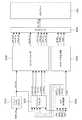
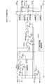
図26は、前記特許文献1に記載された従来の半導体記憶装置の要部構成のブロック図である。 FIG. 26 is a block diagram of a main part configuration of a conventional semiconductor memory device described in
同図において、RACはロウアドレスカウンタ、バンク0、バンク1、・・・、バンク14、バンク15はメモリバンク、WADD<6:0>はワード線アドレス、WRAC<6:0>はリフレッシュワード線アドレス、BSEL<15:0>はバンクセレクト信号、RBSEL<15:0>はリフレッシュバンクセレクト信号である。 In the figure, RAC is a row address counter,
本構成によって、前記バンクセレクト信号BSEL<15:0>によって指定されるメモリバンクとは異なるメモリバンクを、前記リフレッシュバンクセレクト信号RBSEL<15:0>によって選択することで、外部アクセスと同時にリフレッシュを行うことが可能である。外部アクセスされるメモリバンクとリフレッシュしようとするメモリバンクとが衝突する場合には、当該メモリバンクのリフレッシュは不可能であるので、当該半導体記憶装置が搭載されるシステム(図示せず)においてバンク競合を回避している。 With this configuration, by selecting a memory bank different from the memory bank specified by the bank select signal BSEL <15: 0> by the refresh bank select signal RBSEL <15: 0>, refresh is performed simultaneously with external access. Is possible. When a memory bank to be refreshed collides with a memory bank to be refreshed, the memory bank cannot be refreshed. Therefore, a bank conflict occurs in a system (not shown) in which the semiconductor memory device is mounted. Is avoiding.
また、各メモリバンクに対応するロウアドレスカウンタRACに、各メモリバンク内のワード線のうちのリフレッシュされたワード線を独立に記憶させている。これによって、前記ロウアドレスカウンタRACにおいて、各メモリバンク内のリフレッシュされるワード線のアドレス管理を行うので、システム側では、各メモリバンク内のワード線のアドレス管理を意識することが不要となる。 The row address counter RAC corresponding to each memory bank stores a refreshed word line among the word lines in each memory bank independently. As a result, the row address counter RAC performs address management of the word lines to be refreshed in each memory bank, so that the system does not need to be aware of address management of the word lines in each memory bank.
従って、前記特許文献1記載の技術では、所定回数のバンク競合を回避して各々のメモリバンクにリフレッシュバンクセレクト信号RBSEL<15:0>を入力することのみによって、当該半導体記憶装置に備えた複数のメモリバンク内の全てのメモリセルのリフレッシュが可能となる。ここで、例えば、各メモリバンク内に128本のワード線を備えている場合には、128のリフレッシュコマンドがメモリセルのセル電荷保持時間内に各メモリバンク毎に入力されるようにシステム側でバンク競合を回避すれば、全メモリセルのリフレッシュが保証される。
しかしながら、メモリバンク構成を用いない半導体記憶装置においては、当該半導体記憶装置内のメモリブロックへのブロック単位でのアクセスをシステム側が行うことができないので、前記特許文献1記載の技術によって、外部アクセスメモリブロックに対するアクセスと内部リフレッシュメモリブロックに対するアクセスとの競合をシステム側が調停することは不可能である。 However, in a semiconductor memory device that does not use a memory bank configuration, the system side cannot access the memory blocks in the semiconductor memory device in units of blocks. It is impossible for the system side to arbitrate contention between access to the block and access to the internal refresh memory block.
また、前記特許文献1記載の技術では、各々のメモリバンクに対応したロウアドレスカウンタを半導体記憶装置内に分散配置するので、当該半導体記憶装置の面積増大が問題となる。 In the technique disclosed in
さらに、システム側がバンク競合のみを意識してリフレッシュを管理した場合、システム側は各メモリバンク内のワード線のリフレッシュ情報を認識していないので、当該半導体記憶装置にリフレッシュバンクセレクト信号RBSEL<15:0>を入力し続けることになる。これによって、メモリセルのセル電荷保持時間内に必要なリフレッシュ回数以上のリフレッシュが行われて消費電流が増大してしまうという課題がある。これを回避するには、リフレッシュを停止するようにシステム側から複雑なリフレッシュ管理を行うか、DRAM内部で制御を行う必要があるが、前記特許文献1にはこれらの管理や制御については一切開示されていない。 Further, when the system side manages the refresh only in consideration of the bank conflict, the system side does not recognize the refresh information of the word lines in each memory bank, so that the refresh bank select signal RBSEL <15: It will continue to input 0>. As a result, there is a problem in that refreshing is performed more than the number of refreshes required within the cell charge retention time of the memory cell, resulting in an increase in current consumption. In order to avoid this, it is necessary to perform complex refresh management from the system side so as to stop refreshing or control inside the DRAM. However, the above-mentioned
本発明は、前記の課題に着目してなされたのもであり、その目的は、メモリバンク構成を用いない半導体記憶装置において、当該半導体記憶装置が搭載されるシステム側が内部リフレッシュワード線アドレスを意識することなく、かつ、通常ランダム動作・ページ動作・プリチャージ動作及びそれらの混合アクセスのような様々な外部アクセスと、内部同時リフレッシュとの競合の調停が可能な半導体記憶装置を省面積で実現することにある。更には、上記の目的に加えて、メモリセルのセル電荷保持時間内での全メモリセルのリフレッシュを必要最小限の回数で保障することにある。 The present invention has been made paying attention to the above-mentioned problems, and its purpose is to make the system side on which the semiconductor memory device is mounted aware of the internal refresh word line address in a semiconductor memory device not using the memory bank configuration. In addition, a semiconductor memory device capable of arbitrating contention between various external accesses such as normal random operation, page operation, precharge operation, and mixed access thereof and internal simultaneous refresh in a small area is realized. is there. Furthermore, in addition to the above-mentioned object, the refresh of all the memory cells within the cell charge holding time of the memory cells is ensured with the minimum necessary number of times.
前記の目的を達成するために、本発明では、同時に1本のみが活性化される複数のワード線を有する複数のメモリブロックを備えた半導体記憶装置において、前記複数のメモリブロックのうち、リフレッシュを行う2つ以上のメモリブロックを選択する複数のリフレッシュメモリブロックカウンタと、前記2つ以上のメモリブロックに対して共通な共通ワード線アドレスを生成するリフレッシュワード線カウンタと、外部アクセスと内部リフレッシュとの調停を行う調停回路とを新たに備え、前記複数のリフレッシュメモリブロックカウンタと前記リフレッシュワード線カウンタとを用いて、リフレッシュ対象のメモリブロック及びその内部のワード線を示す第1のワード線アドレスを少なくとも1つ以上生成し、外部から当該半導体記憶装置内部のメモリブロック内のワード線へのアクセスが行われる期間に、前記少なくとも1つ以上の第1のワード線アドレスの示すワード線のリフレッシュを行うように調停する構成を採用する。 In order to achieve the above object, according to the present invention, in a semiconductor memory device having a plurality of memory blocks having a plurality of word lines that are activated at the same time, one of the plurality of memory blocks is refreshed. A plurality of refresh memory block counters for selecting two or more memory blocks to be performed; a refresh word line counter for generating a common word line address for the two or more memory blocks; and external access and internal refresh An arbitration circuit for performing arbitration, and using the plurality of refresh memory block counters and the refresh word line counter, at least a first word line address indicating a memory block to be refreshed and a word line therein is provided. Generate one or more semiconductor memory devices from outside During a period in which access to the word line inside the memory block is performed, employing a configuration in which arbitration to perform refresh of the at least one first word line the word line indicated by the address.
具体的に、請求項1記載の発明の半導体記憶装置は、マトリックス状に配置された複数のメモリセルと、前記複数のメモリセルの行に各々対応する複数のワード線と、前記複数のメモリセルの列に各々対応する複数のビット線と、前記複数のメモリセルの列に各々対応する複数のセンスアンプとによって構成され、前記複数のワード線のうち、同時に1本のみのワード線が活性化される複数のメモリブロックと、2つ以上のメモリブロックのブロックアドレスを生成して、前記複数のメモリブロックのうち、リフレッシュを行う2つ以上のメモリブロックを選択する複数のリフレッシュメモリブロックカウンタと、前記2つ以上のメモリブロックに対して共通な共通ワード線アドレスを生成するリフレッシュワード線カウンタと、前記2つ以上のブロックアドレスと前記共通ワード線アドレスとに基づいて、少なくとも1つ以上の第1のワード線アドレスを生成し、外部から供給される第2のワード線アドレスの示すワード線に対してアクセスされる期間に、前記少なくとも1つ以上の第1のワード線アドレスの示す各々のワード線のリフレッシュを行うように調停する調停回路とを備えたことを特徴とする。 Specifically, the semiconductor memory device according to the first aspect of the present invention includes a plurality of memory cells arranged in a matrix, a plurality of word lines respectively corresponding to a row of the plurality of memory cells, and the plurality of memory cells. A plurality of bit lines each corresponding to each of the plurality of columns and a plurality of sense amplifiers corresponding to each of the plurality of memory cell columns, and only one word line among the plurality of word lines is activated at the same time A plurality of memory blocks, a block address of two or more memory blocks, and a plurality of refresh memory block counters for selecting two or more memory blocks to be refreshed among the plurality of memory blocks; A refresh word line counter for generating a common word line address common to the two or more memory blocks; At least one first word line address is generated based on the block address and the common word line address, and the word line indicated by the second word line address supplied from the outside is accessed. And an arbitration circuit that arbitrates to refresh each word line indicated by the at least one or more first word line addresses during the period.
請求項2記載の発明は、前記請求項1記載の半導体記憶装置において、前記調停回路は、前記複数のリフレッシュメモリブロックカウンタで選択された2つ以上のメモリブロックのうちの何れか1つのメモリブロックと、前記第2のワード線アドレスに対応し外部からのアクセスが行われるメモリブロックとが一致するとき、当該メモリブロックのリフレッシュを停止させるように調停することを特徴とする。 According to a second aspect of the present invention, in the semiconductor memory device according to the first aspect, the arbitration circuit is any one of two or more memory blocks selected by the plurality of refresh memory block counters. When the memory block corresponding to the second word line address and accessed from the outside coincides, arbitration is performed so as to stop refreshing of the memory block.
請求項3記載の発明は、前記請求項1記載の半導体記憶装置において、前記複数のリフレッシュメモリブロックカウンタは、リフレッシュ実行後に毎回カウントアップされ、前記リフレッシュワード線カウンタは、全てのメモリブロックに対してリフレッシュが完了した後にカウントアップされることを特徴とする。 According to a third aspect of the present invention, in the semiconductor memory device according to the first aspect, the plurality of refresh memory block counters are counted up every time after refresh execution, and the refresh word line counter is applied to all memory blocks. The counter is counted up after the refresh is completed.
請求項4記載の発明は、前記請求項1記載の半導体記憶装置において、当該半導体記憶装置には、その外部から所定の周期毎にリフレッシュ要求が入力され、前記所定の周期は、当該半導体記憶装置に備えた複数のメモリブロックのうち、リフレッシュが完了していないメモリブロックが1つ以下となる周期であることを特徴とする。 According to a fourth aspect of the present invention, in the semiconductor memory device according to the first aspect, a refresh request is input to the semiconductor memory device every predetermined cycle from the outside, and the predetermined cycle is the semiconductor memory device. Among the plurality of memory blocks prepared in the above, the cycle is such that one or less memory blocks have not been refreshed.
請求項5記載の発明は、前記請求項4記載の半導体記憶装置において、当該半導体記憶装置の外部からのリフレッシュ要求が入力されたとき、前記複数のリフレッシュメモリブロックカウンタの各々には、リフレッシュが完了していないメモリブロックのブロックアドレスが共通のアドレスとして記憶されていることを特徴とする。 According to a fifth aspect of the present invention, in the semiconductor memory device according to the fourth aspect, when a refresh request is input from the outside of the semiconductor memory device, refresh is completed in each of the plurality of refresh memory block counters. A block address of memory blocks that are not yet stored is stored as a common address.
請求項6記載の発明は、前記請求項1記載の半導体記憶装置において、当該半導体記憶装置の外部からのリフレッシュ要求が入力される毎に、前記複数のリフレッシュメモリブロックカウンタがリセットされると共に、前記リフレッシュワード線カウンタがカウントアップされることを特徴とする。 According to a sixth aspect of the present invention, in the semiconductor memory device according to the first aspect, each time a refresh request from the outside of the semiconductor memory device is input, the plurality of refresh memory block counters are reset, and the A refresh word line counter is counted up.
請求項7記載の発明は、前記請求項6記載の半導体記憶装置において、当該半導体記憶装置には、電源立ち上げ後、又はセルフリフレッシュからの復帰後の通常動作開始の直前に、1回のダミー外部リフレッシュ要求が入力されることを特徴とする。 According to a seventh aspect of the present invention, in the semiconductor memory device according to the sixth aspect of the present invention, the semiconductor memory device includes a single dummy immediately after the power is turned on or immediately after the normal operation is started after returning from the self-refresh. An external refresh request is input.
請求項8記載の発明は、前記請求項1記載の半導体記憶装置において、前記複数のリフレッシュメモリブロックカウンタは、リフレッシュ実行後に毎回カウントアップされ、前記調停回路は、全てのメモリブロックに対してリフレッシュが完了した後には、次に前記リフレッシュワード線カウンタがカウントアップされるまで、内部リフレッシュ動作を停止するように調停することを特徴とする。 According to an eighth aspect of the present invention, in the semiconductor memory device according to the first aspect, the plurality of refresh memory block counters are counted up every time refresh is performed, and the arbitration circuit refreshes all memory blocks. After completion, the internal refresh operation is arbitrated until the refresh word line counter is counted up next time.
請求項9記載の発明は、前記請求項1記載の半導体記憶装置において、2個のリフレッシュメモリブロックカウンタは、1対のインクリメントカウンタとデクリメントカウンタとによって構成されることを特徴とする。 According to a ninth aspect of the present invention, in the semiconductor memory device according to the first aspect, the two refresh memory block counters include a pair of increment counters and decrement counters.
請求項10記載の発明は、前記請求項9記載の半導体記憶装置において、前記調停回路は、前記インクリメントカウンタの値が前記デクリメントカウンタの値よりも大きくなった時に、全てのメモリブロックのリフレッシュが完了したことを示すフラグを発生することを特徴とする。 According to a tenth aspect of the present invention, in the semiconductor memory device according to the ninth aspect, when the value of the increment counter is larger than the value of the decrement counter, the arbitration circuit completes refresh of all memory blocks. It is characterized by generating a flag indicating that this has occurred.
請求項11記載の発明は、前記請求項9記載の半導体記憶装置において、当該半導体記憶装置の外部からのリフレッシュ要求が入力されたとき、前記インクリメントカウンタの値と前記デクリメントカウンタの値とが一致する場合、前記調停回路は、前記インクリメントカウンタ及び前記デクリメントカウンタが示すメモリブロックを外部リフレッシュアクセスサイクルでリフレッシュするように調停することを特徴とする。 The invention according to
請求項12記載の発明は、前記請求項1記載の半導体記憶装置において、セルフリフレッシュ時に、前記複数のリフレッシュメモリブロックカウンタは、前記リフレッシュワード線カウンタのキャリー出力信号に応じてカウントアップされるように切り替えられることを特徴とする。 According to a twelfth aspect of the present invention, in the semiconductor memory device according to the first aspect, during the self-refresh, the plurality of refresh memory block counters are counted up according to a carry output signal of the refresh word line counter. It can be switched.
請求項13記載の発明は、前記請求項12記載の半導体記憶装置において、前記複数のリフレッシュメモリブロックカウンタ及び前記リフレッシュワード線カウンタの各々は、セルフリフレッシュ周期でカウントアップされることを特徴とする。 According to a thirteenth aspect of the present invention, in the semiconductor memory device according to the twelfth aspect, each of the plurality of refresh memory block counters and the refresh word line counter is counted up in a self-refresh cycle.
請求項14記載の発明は、前記請求項1記載の半導体記憶装置において、当該半導体記憶装置の外部からの外部制御によって、前記複数のリフレッシュメモリブロックカウンタは、前記リフレッシュワード線カウンタのキャリー出力信号に応じてカウントアップされるように切り替えられることを特徴とする。 According to a fourteenth aspect of the present invention, in the semiconductor memory device according to the first aspect, the plurality of refresh memory block counters are set to carry output signals of the refresh word line counter by external control from the outside of the semiconductor memory device. It is characterized by being switched so as to be counted up accordingly.
請求項15記載の発明は、前記請求項1記載の半導体記憶装置において、さらに、当該半導体記憶装置の外部から供給された前記第2のワード線アドレスの記憶手段を備え、
前記調停回路は、前記第1のワード線アドレスと、前記記憶手段に記憶された1つ以上の第2のワード線アドレスとを比較し、一致する場合は前記第1のワード線アドレスの示すワード線のリフレッシュをスキップするように調停することを特徴とする。According to a fifteenth aspect of the present invention, in the semiconductor memory device according to the first aspect of the present invention, the semiconductor memory device further includes storage means for storing the second word line address supplied from outside the semiconductor memory device.
The arbitration circuit compares the first word line address with one or more second word line addresses stored in the storage means, and if they match, the word indicated by the first word line address Arbitration is performed to skip line refresh.
請求項16記載の発明は、前記請求項15記載の半導体記憶装置において、前記記憶手段は、外部アクセスメモリブロックアドレス記憶手段と、前記第1及び第2のワード線アドレスの一致フラグ記憶手段とによって構成されることを特徴とする。 According to a sixteenth aspect of the present invention, in the semiconductor memory device according to the fifteenth aspect, the storage means includes an external access memory block address storage means and a match flag storage means for the first and second word line addresses. It is characterized by being configured.
請求項17記載の発明は、前記請求項15記載の半導体記憶装置において、前記記憶手段は、当該半導体記憶装置の外部からリフレッシュ要求が入力される度にリセットされることを特徴とする。 According to a seventeenth aspect of the present invention, in the semiconductor memory device according to the fifteenth aspect, the storage unit is reset every time a refresh request is input from the outside of the semiconductor memory device.
請求項18記載の発明は、前記請求項1記載の半導体記憶装置において、前記第1のワード線アドレスは、第1のプリデコード信号線を用いて伝送されると共に、前記第2のワード線アドレスは、第2のプリデコード信号線を用いて伝送され、前記第1及び第2のプリデコード信号線の信号線数は同数であることを特徴とする。 According to an eighteenth aspect of the present invention, in the semiconductor memory device according to the first aspect, the first word line address is transmitted using a first predecode signal line, and the second word line address is transmitted. Is transmitted using a second predecode signal line, and the number of signal lines of the first and second predecode signal lines is the same.
請求項19記載の発明は、前記請求項1記載の半導体記憶装置において、前記複数のリフレッシュメモリブロックカウンタは、複数対のインクリメントカウンタとデクリメントカウンタとによって構成され、前記複数のメモリセルによって構成される複数のメモリアレイを複数の領域に分割したそれぞれの領域に対して、1対のインクリメントカウンタ及びデクリメントカウンタが割り当てられることを特徴とする。 According to a nineteenth aspect of the present invention, in the semiconductor memory device according to the first aspect, the plurality of refresh memory block counters are composed of a plurality of pairs of increment counters and decrement counters, and are composed of the plurality of memory cells. A pair of increment counters and decrement counters is assigned to each area obtained by dividing a plurality of memory arrays into a plurality of areas.
請求項20記載の発明の半導体記憶装置は、マトリックス状に配置された複数のメモリセルと、前記複数のメモリセルの行に各々対応する複数のワード線と、前記複数のメモリセルの列に各々対応する複数のビット線と、前記複数のメモリセルの列に各々対応する複数のセンスアンプとによって構成され、前記複数のワード線のうち、同時に1本のみのワード線が活性化される複数のメモリブロックと、前記複数のメモリブロックに共通なブロックアドレスを生成する複数のリフレッシュメモリブロックカウンタと、前記複数のメモリブロックのうち、2つ以上のメモリブロックに対して共通な共通ワード線アドレスを生成するリフレッシュワード線カウンタと、前記ブロックアドレスと前記共通ワード線アドレスとに基づいて、少なくとも1つ以上の第1のワード線アドレスを生成し、外部から供給される第2のワード線アドレスの示すワード線に対してアクセスされる期間に、前記少なくとも1つ以上の第1のワード線アドレスの示す各々のワード線のリフレッシュを行うように調停する調停回路とを備えたことを特徴とする。 According to a twenty-second aspect of the present invention, a plurality of memory cells arranged in a matrix, a plurality of word lines respectively corresponding to a row of the plurality of memory cells, and a column of the plurality of memory cells are provided. A plurality of corresponding bit lines and a plurality of sense amplifiers respectively corresponding to the columns of the plurality of memory cells, and a plurality of word lines are activated at the same time among the plurality of word lines. A memory block, a plurality of refresh memory block counters that generate a block address common to the plurality of memory blocks, and a common word line address that is common to two or more memory blocks among the plurality of memory blocks Based on the refresh word line counter, the block address and the common word line address The at least one first word line address is generated in a period in which one or more first word line addresses are generated and accessed from a word line indicated by the second word line address supplied from the outside. And an arbitration circuit that arbitrates to refresh each word line shown.
請求項21記載の発明は、前記請求項1〜20の何れか一項に記載の半導体記憶装置において、前記調停回路は、当該半導体記憶装置の外部からアクセスされるページアクセス期間中に、前記少なくとも1つ以上の第1のワード線アドレスの示す各々のワード線のリフレッシュを行うように調停することを特徴とする。 According to a twenty-first aspect of the present invention, in the semiconductor memory device according to any one of the first to twentieth aspects, the arbitration circuit includes the at least a page access period accessed from outside the semiconductor memory device. Arbitration is performed so that each word line indicated by one or more first word line addresses is refreshed.
請求項22記載の発明は、前記請求項21記載の半導体記憶装置において、さらに、ロウ制御回路を備え、前記ロウ制御回路は、複数サイクルにわたって外部から入力されるロウアクセスコマンド信号のイネーブルクロック数をカウントし、所定の回数毎に内部同時リフレッシュコマンドを発行することを特徴とする。 The invention according to claim 22 is the semiconductor memory device according to claim 21, further comprising a row control circuit, wherein the row control circuit determines the number of enable clocks of a row access command signal input from the outside over a plurality of cycles. It counts and issues an internal simultaneous refresh command every predetermined number of times.
請求項23記載の発明は、前記請求項1〜22の何れか一項に記載の半導体記憶装置において、前記調停回路は、プリチャージ期間であることを検知して、複数の第1のワード線アドレスの示すワード線の同時リフレッシュを行うように調停することを特徴とする。 According to a twenty-third aspect of the present invention, in the semiconductor memory device according to any one of the first to twenty-second aspects, the arbitration circuit detects a precharge period and detects a plurality of first word lines. Arbitration is performed so as to simultaneously refresh the word line indicated by the address.
請求項24記載の発明は、前記請求項22又は23記載の半導体記憶装置において、前記ロウ制御回路は、外部から入力されるロウアクセスコマンド信号のディスネーブルクロック数をカウントし、所定の回数毎に内部同時リフレッシュコマンドを発行することを特徴とする。 According to a twenty-fourth aspect of the present invention, in the semiconductor memory device according to the twenty-second or twenty-third aspect, the row control circuit counts the number of disable clocks of a row access command signal input from the outside, and every predetermined number of times. An internal simultaneous refresh command is issued.
請求項25記載の発明は、前記請求項21〜24の何れか一項に記載の半導体記憶装置において、当該半導体記憶装置の動作がプリチャージ期間のとき、当該半導体記憶装置に入力される入力クロック数は、所定の制限数以下であることを特徴とする。 According to a twenty-fifth aspect of the invention, in the semiconductor memory device according to any one of the twenty-first to twenty-fourth aspects, an input clock input to the semiconductor memory device when the operation of the semiconductor memory device is in a precharge period. The number is less than a predetermined limit number.
請求項26記載の発明は、前記請求項25記載の半導体記憶装置において、最小ランダムサイクルが2クロックのとき、プリチャージ期間の入力クロック数が奇数であることを特徴とする。 According to a twenty-sixth aspect of the present invention, in the semiconductor memory device according to the twenty-fifth aspect, when the minimum random cycle is two clocks, the number of input clocks in the precharge period is an odd number.
請求項27記載の発明は、前記請求項25記載の半導体記憶装置において、最小ランダムサイクルが2クロックのとき、プリチャージ期間の入力クロック数が所定の回数以上となる場合には、その入力クロック数は奇数であることを特徴とする。 According to a twenty-seventh aspect of the present invention, in the semiconductor memory device according to the twenty-fifth aspect, when the minimum random cycle is two clocks and the number of input clocks in the precharge period is a predetermined number or more, the number of input clocks Is an odd number.
請求項28記載の発明の内部リフレッシュ停止方法は、複数のマトリックス配列されたメモリセルと、複数のワード線と、複数のビット線と、複数のセンスアンプとから構成されて、同時に1本のみの前記ワード線が活性化されるメモリブロックを複数備えた半導体記憶装置における内部リフレッシュ停止方法において、前記複数のメモリブロックを順番に内部リフレッシュするアドレスを発生する複数のブロックカウンタの値の大小を検出する工程と、前記工程の検出結果に基づいて、リフレッシュを一時停止する工程とを有することを特徴とする。 An internal refresh stop method according to a twenty-eighth aspect comprises a plurality of memory cells arranged in a matrix, a plurality of word lines, a plurality of bit lines, and a plurality of sense amplifiers. In a method of stopping internal refresh in a semiconductor memory device having a plurality of memory blocks in which the word line is activated, the magnitudes of values of a plurality of block counters for generating addresses for internally refreshing the plurality of memory blocks in order are detected. And a step of temporarily stopping refreshing based on a detection result of the step.
請求項29記載の発明は、前記請求項28記載の内部リフレッシュ停止方法において、前記複数のブロックカウンタが、1対若しくは複数対のインクリメントカウンタとデクリメントカウンタとで構成された場合に、内部リフレッシュが実行される度に前記インクリメントカウンタ及びデクリメントカウンタのカウントを行うと共に、前記インクリメントカウンタのカウンタ値及び前記デクリメントカウンタのカウンタ値の大小を比較する工程と、前記インクリメントカウンタのカウンタ値が前記デクリメントカウンタのカウンタ値よりも大きくなった時点で内部リフレッシュを一時停止する工程とを有することを特徴とする。 A twenty-ninth aspect of the invention is the internal refresh stopping method according to the twenty-eighth aspect, wherein the internal refresh is performed when the plurality of block counters are configured with one or a plurality of pairs of increment counters and decrement counters. The increment counter and the decrement counter are counted each time the counter value of the increment counter and the counter value of the decrement counter are compared, and the counter value of the increment counter is the counter value of the decrement counter. And a step of temporarily suspending the internal refresh when it becomes larger.
請求項30記載の発明は、前記請求項28記載の内部リフレッシュ停止方法において、内部リフレッシュの一時停止の状態は、外部からのリフレッシュコマンドが発行されるまで継続されることを特徴とする。 According to a thirty-third aspect of the present invention, in the internal refresh stopping method according to the twenty-eighth aspect, the state of the internal refresh pause is continued until an external refresh command is issued.
請求項31記載の発明の外部アクセスと内部リフレッシュとの競合処理方法は、複数のマトリックス配列されたメモリセルと、複数のワード線と、複数のビット線と、複数のセンスアンプとから構成されて、同時に1本のみの前記ワード線が活性化される複数のメモリブロックと、前記複数のメモリブロックを順番に内部リフレッシュするアドレスを発生する複数のブロックカウンタとを備えた半導体記憶装置における外部アクセスと内部リフレッシュとの競合処理方法において、外部アクセスされるメモリブロックと内部リフレッシュメモリブロックとの衝突を検出する工程と、前記工程で衝突を検出したとき、内部リフレッシュ及び前記ブロックカウンタのカウントを停止する工程とを有することを特徴とする。 A contention processing method for external access and internal refresh according to a thirty-first aspect of the invention comprises a plurality of memory cells arranged in a matrix, a plurality of word lines, a plurality of bit lines, and a plurality of sense amplifiers. External access in a semiconductor memory device comprising a plurality of memory blocks in which only one word line is activated at the same time, and a plurality of block counters for generating addresses for internally refreshing the plurality of memory blocks in sequence, In a conflict processing method with internal refresh, a step of detecting a collision between an externally accessed memory block and an internal refresh memory block, and a step of stopping the internal refresh and counting of the block counter when a collision is detected in the step It is characterized by having.
請求項32記載の発明は、前記請求項31記載の外部アクセスと内部リフレッシュとの競合処理方法において、外部アクセスされるメモリブロックと内部リフレッシュメモリブロックとの衝突が外部リフレッシュまで継続した場合、外部リフレッシュサイクルで前記衝突メモリブロックをリフレッシュすることを特徴とする。 According to a thirty-second aspect of the present invention, in the conflict processing method between the external access and the internal refresh according to the thirty-first aspect, if the collision between the externally accessed memory block and the internal refresh memory block continues until the external refresh, the external refresh The collision memory block is refreshed in a cycle.
請求項33記載の発明のカウンタ初期化手法は、複数のマトリックス配列されたメモリセルと、複数のワード線と、複数のビット線と、複数のセンスアンプとから構成されて、同時に1本のみの前記ワード線が活性化される複数のメモリブロックと、前記複数のメモリブロックを順番に内部リフレッシュするアドレスを発生する複数のブロックカウンタとを備えた半導体記憶装置におけるカウンタ初期化方法において、外部リフレッシュコマンドの入力を検出する工程と、前記工程で外部リフレッシュコマンドの入力を検出したとき、前記複数のブロックカウンタを初期化する工程とを有することを特徴とする。 A counter initialization method according to a thirty-third aspect is composed of a plurality of memory cells arranged in a matrix, a plurality of word lines, a plurality of bit lines, and a plurality of sense amplifiers. An external refresh command in a counter initialization method in a semiconductor memory device comprising: a plurality of memory blocks in which the word lines are activated; and a plurality of block counters for generating addresses for internally refreshing the plurality of memory blocks in order. And a step of initializing the plurality of block counters when an input of an external refresh command is detected in the step.
請求項34記載の発明の外部リフレッシュのリフレッシュアドレス検出方法は、複数のマトリックス配列されたメモリセルと、複数のワード線と、複数のビット線と、複数のセンスアンプとから構成されて、同時に1本のみの前記ワード線が活性化される複数のメモリブロックと、前記複数のメモリブロックを順番に内部リフレッシュするアドレスを発生する複数のブロックカウンタとを備えた半導体記憶装置における外部リフレッシュのリフレッシュアドレス検出方法において、外部リフレッシュサイクルを検出する工程と、前記工程で外部リフレッシュサイクルを検出したとき、前記複数のブロックカウンタに共通するアドレスをリフレッシュする工程とを有することを特徴とする。 A refresh address detection method for external refresh according to a thirty-fourth aspect of the present invention comprises a plurality of memory cells arranged in a matrix, a plurality of word lines, a plurality of bit lines, and a plurality of sense amplifiers. Refresh address detection for external refresh in a semiconductor memory device comprising a plurality of memory blocks in which only one word line is activated and a plurality of block counters for generating addresses for internally refreshing the plurality of memory blocks in order The method includes a step of detecting an external refresh cycle and a step of refreshing an address common to the plurality of block counters when the external refresh cycle is detected in the step.
請求項35記載の発明の外部リフレッシュ実行選択方法は、複数のマトリックス配列されたメモリセルと、複数のワード線と、複数のビット線と、複数のセンスアンプとから構成されて、同時に1本のみの前記ワード線が活性化される複数のメモリブロックと、前記複数のメモリブロックを順番に内部リフレッシュするアドレスを発生する複数のブロックカウンタとを備えた半導体記憶装置における外部リフレッシュ実行選択方法において、前記複数のブロックカウンタが、1対若しくは複数対のインクリメントカウンタとデクリメントカウンタとで構成された場合に、内部リフレッシュが実行される度に前記インクリメントカウンタ及びデクリメントカウンタのカウントを行うと共に、前記インクリメントカウンタのカウンタ値及び前記デクリメントカウンタのカウンタ値の大小を比較する工程と、前記工程において、前記インクリメントカウンタのカウンタ値と前記デクリメントカウンタのカウンタ値とが一致する場合に、外部リフレッシュを実行する工程とを有することを特徴とする。 An external refresh execution selection method according to a thirty-fifth aspect of the present invention comprises a plurality of memory cells arranged in a matrix, a plurality of word lines, a plurality of bit lines, and a plurality of sense amplifiers, and only one at a time. In the external refresh execution selection method in a semiconductor memory device, comprising: a plurality of memory blocks in which the word lines are activated; and a plurality of block counters that generate addresses for internally refreshing the plurality of memory blocks in order. When a plurality of block counters are composed of one or more pairs of increment counters and decrement counters, the increment counters and decrement counters are counted each time an internal refresh is executed, and the counters of the increment counters Value and A step of comparing the magnitudes of the counter values of the increment counter, and a step of executing an external refresh when the count value of the increment counter and the counter value of the decrement counter match in the step. To do.
以上により、請求項1記載の発明では、2つ以上のメモリブロックのブロックアドレスを生成する複数のリフレッシュメモリブロックカウンタと、複数のメモリブロックで共通な共通ワード線アドレス(ブロック内ワード線アドレス)を生成するリフレッシュワード線カウンタとを用いて、リフレッシュ対象のメモリブロック及びその内部のワード線を示す第1のワード線アドレス(リフレッシュアドレス)を少なくとも1つ以上生成する。そのため、メモリバンク構成を用いない半導体記憶装置であっても、例えば、外部からアクセスされるメモリブロックと前記リフレッシュメモリブロックカウンタの指し示すメモリブロックとを比較することによって、外部からのアクセスが行われるメモリブロック(外部アクセスブロック)と、リフレッシュを行おうとするメモリブロック(内部リフレッシュメモリブロック)との調停を行うことが可能となる。また、外部アクセスブロックと内部リフレッシュメモリブロックとが衝突した場合であっても、衝突する第1のワード線アドレス以外の第1のワード線アドレスの示すワード線のリフレッシュは可能であるので、外部アクセスと同時にリフレッシュを行うことができる。さらに、前記リフレッシュメモリカウンタ及び前記リフレッシュワード線カウンタは、メモリブロック毎に設けるのではなく、当該半導体記憶装置内の複数のメモリブロックで共用するので、面積の削減が可能となる。 As described above, according to the first aspect of the present invention, a plurality of refresh memory block counters that generate block addresses of two or more memory blocks and a common word line address (in-block word line address) common to the plurality of memory blocks are obtained. Using the generated refresh word line counter, at least one or more first word line addresses (refresh addresses) indicating the memory block to be refreshed and the word lines therein are generated. Therefore, even in a semiconductor memory device that does not use a memory bank configuration, for example, a memory that is accessed from the outside by comparing a memory block that is accessed from the outside with a memory block that is indicated by the refresh memory block counter. Arbitration between a block (external access block) and a memory block (internal refresh memory block) to be refreshed can be performed. Even if the external access block and the internal refresh memory block collide, the word line indicated by the first word line address other than the colliding first word line address can be refreshed. At the same time, refresh can be performed. Furthermore, since the refresh memory counter and the refresh word line counter are not provided for each memory block but are shared by a plurality of memory blocks in the semiconductor memory device, the area can be reduced.
請求項2記載の発明では、リフレッシュしようとする複数のメモリブロックのうちの何れか1つのメモリブロックと、外部からのアクセスが行われるメモリブロックとが一致した場合には、当該メモリブロックのリフレッシュは停止されるが、前記リフレッシュをしようとする複数のメモリブロックのうちの他のメモリブロックにおけるリフレッシュは実行されるので、外部からのアクセスと同時に少なくとも1つのメモリブロック内のワード線のリフレッシュを実行するように調停することができる。 According to the second aspect of the present invention, when any one of the plurality of memory blocks to be refreshed matches the memory block to be accessed from the outside, the refresh of the memory block is performed Although it is stopped, refresh in the other memory blocks among the plurality of memory blocks to be refreshed is executed, so that the word lines in at least one memory block are refreshed simultaneously with external access. So that you can mediate.
請求項3記載の発明では、外部アクセスブロックと内部リフレッシュメモリブロックとの衝突が発生した場合には、リフレッシュメモリブロックカウンタはカウントアップされないので、リフレッシュ未実行のメモリブロックが記憶でき、かつ特定のブロック内ワード線アドレスに対して全メモリブロック分のリフレッシュが完了することを保障できる。 According to the third aspect of the present invention, when a collision between the external access block and the internal refresh memory block occurs, the refresh memory block counter is not counted up, so that a memory block that has not been refreshed can be stored and a specific block is stored. It can be ensured that refresh for all memory blocks is completed with respect to the inner word line address.
請求項4記載の発明では、所定の周期で外部からのリフレッシュ要求(外部リフレッシュコマンド)が入力されたサイクルの直前には、あるブロック内ワード線アドレスに対して多くても1ブロックのワード線のみが未リフレッシュ状態であるので、外部からのオートリフレッシュサイクルで当該未リフレッシュワード線のリフレッシュを実行でき、外部リフレッシュ周期内で確実に特定のブロック内ワード線アドレスに対して全ブロックのリフレッシュを完了させることができる。 According to the fourth aspect of the present invention, immediately before a cycle in which an external refresh request (external refresh command) is input at a predetermined cycle, only a word line of at most one block with respect to a word line address within a block is included. Is in an unrefreshed state, the unrefreshed word line can be refreshed in an external auto-refresh cycle, and the refresh of all the blocks is completely completed for a specific word line address in the block within the external refresh cycle. be able to.
請求項5記載の発明では、リフレッシュメモリブロックカウンタ自体に未リフレッシュのメモリブロックの記憶機能を持たせることで、余分な記憶用レジスタが不要となり、制御も容易にできる。 According to the fifth aspect of the present invention, since the refresh memory block counter itself has a storage function for an unrefreshed memory block, an extra storage register is not required and control can be facilitated.
請求項6記載の発明では、外部リフレッシュコマンドの入力をトリガにして、リフレッシュメモリブロックカウンタのリセット、及びリフレッシュワード線カウンタのカウントアップをするので、当該半導体記憶装置の内部で外部アクセス回数のカウントを行う必要がなく、カウント回路等を省略できて省面積化できる。 According to the sixth aspect of the present invention, the refresh memory block counter is reset and the refresh word line counter is counted up with the input of the external refresh command as a trigger. Therefore, the external access count is counted inside the semiconductor memory device. There is no need to perform this, and the count circuit and the like can be omitted to save the area.
請求項7記載の発明では、電源立ち上げ後、又はセルフリフレッシュからの復帰後の通常動作開始の直前に、リフレッシュメモリブロックカウンタがリセットされるので、次のリフレッシュ入力時には最大で1ブロックのリフレッシュが完了した状態を保障できる。 According to the seventh aspect of the present invention, the refresh memory block counter is reset immediately after the power is turned on or after the normal operation is started after returning from the self-refresh. Therefore, at the next refresh input, at most one block is refreshed. Can ensure the completed state.
請求項8記載の発明では、外部リフレッシュコマンドの発行周期内で、あるブロック内ワード線アドレスに対して全ブロックのリフレッシュが完了した後は内部リフレッシュが停止するので、必要以上のリフレッシュを防止できて低電力化でき、同時に電荷保持時間内での全ワード線リフレッシュを保障することができる。 According to the eighth aspect of the present invention, since the internal refresh is stopped after the refresh of all the blocks is completed for the word line address in a block within the external refresh command issue cycle, it is possible to prevent an unnecessary refresh. The power can be reduced, and at the same time, all word line refreshes can be ensured within the charge retention time.
請求項9記載の発明では、一対のインクリメントカウンタ及びデクリメントカウンタから成るリフレッシュメモリブロックカウンタによって、外部アクセスブロックと内部リフレッシュメモリブロックとの調停が可能である。 According to the ninth aspect of the present invention, the external access block and the internal refresh memory block can be arbitrated by the refresh memory block counter including a pair of increment counter and decrement counter.
請求項10記載の発明では、全メモリブロックのリフレッシュが完了したことを簡易な論理回路で検出することが可能となる。 According to the tenth aspect of the present invention, it is possible to detect the completion of the refresh of all the memory blocks with a simple logic circuit.
請求項11記載の発明では、インクリメントカウンタの値とデクリメントカウンタの値とが一致するアドレスを検出・保持することが、リフレッシュが完了していないメモリブロックのブロックアドレスを検出・保持する手段として容易に実現できる。また、外部からのリフレッシュ要求時には、最大でも1ブロックの未リフレッシュブロックしか残っていないので、外部リフレッシュ周期内で確実に特定のブロック内ワード線アドレスに対して全メモリブロックのリフレッシュを完了させることができる。 According to the eleventh aspect of the invention, it is easy to detect and hold an address where the value of the increment counter matches the value of the decrement counter as a means for detecting and holding a block address of a memory block for which refresh has not been completed. realizable. Further, at the time of an external refresh request, only one unrefreshed block remains at the maximum, so that all memory blocks can be completely refreshed for a specific word line address within a block within an external refresh cycle. it can.
請求項12記載の発明では、通常動作中のカウンタ動作のトリガは、リフレッシュメモリブロックカウンタについては外部クロック、リフレッシュワード線カウンタについては所定の周期毎の外部リフレッシュコマンドであるが、セルフリフレッシュについてはその両トリガが無いが、リフレッシュワード線カウンタとリフレッシュメモリブロックカウンタとが連動してカウントアップを行う構成をとることによって、内部での1つのトリガを発生すればオートリフレッシュが可能となる。 In the invention described in
請求項13記載の発明では、カウンタ制御のトリガとなる所定の周期毎の外部リフレッシュコマンドが入力されないセルフリフレッシュ時であっても、セルフリフレッシュ周期でカウンタのカウントアップ動作が可能であり、オートリフレッシュが可能となる。 According to the thirteenth aspect of the present invention, the counter can be counted up in the self-refresh cycle even when the external refresh command is not input every predetermined cycle as a trigger for counter control, and the auto-refresh can be performed. It becomes possible.
請求項14記載の発明では、通常動作中では、所定の周期毎の外部リフレッシュコマンドの入力が必要であるが、半導体記憶装置が搭載されるシステムの使用の仕方によっては、特定動作パターン時には、集中リフレッシュを実施する方がオーバーヘッドが少なくなるケースが想定されるので、同時リフレッシュと集中リフレッシュとをシステム側から制御して最適なシステムパフォーマンスを引き出すことが可能である。また、同制御をテスト時に使うことによって、同時リフレッシュ及び集中リフレッシュの両機能を製品の出荷前に予め確認することができる。 According to the fourteenth aspect of the present invention, it is necessary to input an external refresh command every predetermined period during normal operation. However, depending on how the system in which the semiconductor memory device is mounted is used, there is a concentration during a specific operation pattern. Since it is assumed that the overhead is reduced when the refresh is performed, it is possible to control the simultaneous refresh and the centralized refresh from the system side to obtain the optimum system performance. In addition, by using this control at the time of testing, it is possible to confirm both the simultaneous refresh function and the concentrated refresh function before shipping the product.
請求項15記載の発明では、セル電荷保持時間内にリフレッシュすべきワード線が先に外部アクセスされた時には、リフレッシュされたのと等価であるので、当該メモリブロックのリフレッシュをスキップすることで余分な電力消費を抑制できる。 According to the fifteenth aspect of the present invention, when a word line to be refreshed within the cell charge holding time is first externally accessed, it is equivalent to refreshing. Power consumption can be suppressed.
請求項16記載の発明では、一部の第2のワード線アドレスのみを記憶することで記憶手段の面積増大を抑制し、省面積化できる。 In the invention described in claim 16, by storing only a part of the second word line addresses, an increase in the area of the storage means can be suppressed and the area can be saved.
請求項17記載の発明では、外部リフレッシュ要求周期内にアクセスされるワード線アドレスを記憶をするよりもビット数を抑制できるので省面積化できる。 In the invention described in claim 17, since the number of bits can be suppressed as compared with storing the word line address accessed within the external refresh request cycle, the area can be saved.
請求項18記載の発明では、同時リフレッシュを実行するリフレッシュメモリブロックが複数である場合であっても、メモリブロック選択プリデコード信号線を共用できるので面積増大を最小限に抑えることができる。 According to the eighteenth aspect of the present invention, even when there are a plurality of refresh memory blocks that perform simultaneous refresh, the memory block selection predecode signal line can be shared, so that an increase in area can be minimized.
請求項19記載の発明では、外部アクセス時に同時リフレッシュするメモリブロック数を多くできるので、メモリブロック数が多い、若しくはランダムサイクル時間が遅い場合でも、外部リフレッシュ間隔内に、確実に最大1ブロック以外のリフレッシュが完了した状態にでき、外部リフレッシュ周期内に特定のブロック内ワード線アドレスに対して全メモリブロックのリフレッシュを完了させることができる。 In the invention according to claim 19, since the number of memory blocks to be simultaneously refreshed at the time of external access can be increased, even if the number of memory blocks is large or the random cycle time is slow, it is ensured that other than a maximum of one block within the external refresh interval The refresh can be completed, and the refresh of all the memory blocks can be completed for a specific word line address in the block within the external refresh cycle.
請求項20記載の発明では、外部アクセス時及び外部リフレッシュ動作時に同時リフレッシュするメモリブロック数を多くでき、メモリブロック数が多い場合やランダムサイクル時間が遅い場合であっても、外部リフレッシュ間隔内に、確実に最大1ブロック以外のリフレッシュが完了した状態にして、外部リフレッシュ周期内に所定の全メモリブロックのリフレッシュを完了させることができる。 In the invention of
請求項22記載の発明では、ページ動作中に同一メモリブロックに対してアクセスが連続する場合であっても、当該メモリブロック以外のメモリブロックをリフレッシュできるので、ページ動作中であっても同時内部リフレッシュが可能となる。 According to the twenty-second aspect of the present invention, since the memory blocks other than the memory block can be refreshed even when accesses to the same memory block are continued during the page operation, simultaneous internal refresh even during the page operation Is possible.
請求項24記載の発明では、外部アクセスがない状態を検知して、外部アクセスの有無に拘わらず内部リフレッシュを実行することで、外部から内部アクセスをするような管理をしなくても、所定のリフレッシュ周期を守ってオートリフレッシュコマンドを入力さえすれば全セルのセル電荷保持時間内でのリフレッシュを保障できる。 In the invention according to claim 24, it is possible to detect a state where there is no external access, and execute an internal refresh regardless of the presence or absence of the external access, so that the predetermined access can be performed without performing the internal access from the outside. As long as the auto-refresh command is input while keeping the refresh cycle, the refresh within the cell charge holding time of all cells can be guaranteed.
請求項25記載の発明では、任意のページ長に対して同時リフレッシュを実行することができる。 In the invention of claim 25, simultaneous refresh can be executed for any page length.
請求項26記載の発明では、最小ランダムサイクルが2クロックの場合に、任意のページ長に対して同時リフレッシュを実行することができる。 In the invention of claim 26, when the minimum random cycle is 2 clocks, the simultaneous refresh can be executed for any page length.
請求項27記載の発明では、最小ランダムサイクルが2クロックの場合に、任意のページ長に対して同時リフレッシュを実行しつつ、システム性能を律速するようなリード・ライトアクセス制約をなくし、待機状態に入るようなプリチャージ期間の長い状態には内部リフレッシュを実行することができる。 In a twenty-seventh aspect of the present invention, when the minimum random cycle is two clocks, read / write access restrictions that limit system performance are eliminated while simultaneous refresh is executed for an arbitrary page length, and a standby state is established. Internal refresh can be performed in a state where the precharge period is long.
請求項29記載の発明では、ある特定のブロック内ワード線アドレスに対して、全ブロックのリフレッシュの完了を容易に検出できる。 According to the twenty-ninth aspect of the present invention, it is possible to easily detect completion of refresh of all the blocks with respect to a specific intra-block word line address.
請求項30記載の発明では、セルの電荷保持時間内に必要最低限のリフレッシュ回数以上のリフレッシュ実行を停止することができ、低電力化できる。 According to the thirty-third aspect of the present invention, it is possible to stop the refresh execution more than the minimum necessary number of refreshes within the cell charge retention time, thereby reducing the power consumption.
請求項31記載の発明では、同一のワード線が、外部リフレッシュ及び内部リフレッシュされることによるデータ破壊を防止できると同時に、未リフレッシュブロックアドレスがカウンタアドレスとして保持され、かつ衝突をしていないブロックカウンタアドレスのリフレッシュを実行することができる。 In the invention described in claim 31, the same word line can prevent data destruction due to external refresh and internal refresh, and at the same time, a block counter in which an unrefreshed block address is held as a counter address and no collision occurs Address refresh can be performed.
請求項32記載の発明では、外部リフレッシュ周期で、ある特定のブロック内ワード線アドレスに対する全ブロックのリフレッシュの完了を保障することができる。 According to the thirty-second aspect of the present invention, it is possible to guarantee the completion of the refresh of all the blocks with respect to a specific intra-block word line address in the external refresh cycle.
請求項33記載の発明では、カウンタ初期化を簡易に実現することができる。 According to the thirty-third aspect of the present invention, counter initialization can be easily realized.
請求項34記載の発明では、ブロックカウンタ自体に記憶された唯一未リフレッシュブロックアドレスを外部リフレッシュ時に確実にリフレッシュすることができる。 In the invention of claim 34, the only unrefreshed block address stored in the block counter itself can be reliably refreshed at the time of external refresh.
請求項35記載の発明では、ブロックカウンタ自体に記憶されている唯一の未リフレッシュブロックアドレスを外部リフレッシュサイクルで確実にリフレッシュすることができ、外部リフレッシュ周期で、ある特定のブロック内ワード線アドレスに対する全ブロックのリフレッシュの完了を保障することができる。 In the invention described in claim 35, the only unrefreshed block address stored in the block counter itself can be reliably refreshed in the external refresh cycle, and all the word line addresses in a specific block can be refreshed in the external refresh cycle. Completion of block refresh can be ensured.
以上説明したように、本発明によれば、メモリバンク構成を用いない半導体記憶装置において、当該半導体記憶装置が搭載されるシステム側が内部リフレッシュアドレスを意識することなく、外部からのアクセスと内部リフレッシュとの同時実行が省面積・低電力で可能となる。 As described above, according to the present invention, in a semiconductor memory device that does not use a memory bank configuration, external access and internal refresh can be performed without the system side on which the semiconductor memory device is mounted being aware of the internal refresh address. Can be executed simultaneously with reduced area and power consumption.
以下、本発明の実施形態の半導体記憶装置を図面に基づいて説明する。 Hereinafter, a semiconductor memory device according to an embodiment of the present invention will be described with reference to the drawings.
(第1の実施形態)
以下、本発明の第1の実施形態の半導体記憶装置について、図面を参照しながら説明する。(First embodiment)
The semiconductor memory device according to the first embodiment of the present invention will be described below with reference to the drawings.
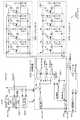
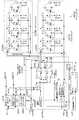
図1は、本発明の第1の実施形態における半導体記憶装置の全体構成のブロック図を示している。 FIG. 1 is a block diagram showing the overall configuration of the semiconductor memory device according to the first embodiment of the present invention.
同図において、100はメモリアレイ、200はロウプリデコーダ(調停回路)、300はリフレッシュカウンタ、400はロウ制御回路、500はタイミング発生回路、600はロウデコーダ(調停回路)、700はアドレスラッチブロックである。 In the figure, 100 is a memory array, 200 is a row predecoder (arbitration circuit), 300 is a refresh counter, 400 is a row control circuit, 500 is a timing generation circuit, 600 is a row decoder (arbitration circuit), and 700 is an address latch block. It is.
当該半導体記憶装置の外部から前記アドレスラッチブロック700に、外部ロウアドレス(第2のワード線アドレス)RADD<11:0>が入力され、前記アドレスラッチブロック700から前記ロウプリデコーダ200及び前記リフレッシュカウンタ300に、外部ロウアドレスラッチ信号AX<11:0>が入力される。 An external row address (second word line address) RADD <11: 0> is input to the address latch block 700 from the outside of the semiconductor memory device, and the row predecoder 200 and the refresh counter are transferred from the
また、当該半導体記憶装置の外部から前記ロウ制御回路400に、外部クロックCLK、外部RASコマンド信号NRAS、外部オートリフレッシュコマンド信号NRAUT、外部リセット信号NRSTが入力され、前記外部リセット信号NRSTは、前記リフレッシュカウンタ300にも入力される。 An external clock CLK, an external RAS command signal NRAS, an external auto-refresh command signal NRAUT, and an external reset signal NRST are input to the
また、前記ロウ制御回路400から前記リフレッシュカウンタ300に、オートリフレッシュフラグAUTF、オートリフレッシュ・プリチャージフラグAUTPRCF、カウンタセレクト信号CNTSELが入力されると共に、前記ロウ制御回路400から前記タイミング発生回路500に、内部RAS信号IRASが入力される。 In addition, an auto refresh flag AUTF, an auto refresh / precharge flag AUTPRCF, and a counter select signal CNTSEL are input from the
また、前記リフレッシュカウンタ300から前記ロウプリデコーダ200に、インクリメントリフレッシュブロックカウンタアドレス(ブロックアドレス)AXU<11:8>、デクリメントリフレッシュブロックカウンタアドレス(ブロックアドレス)AXD<11:8>、内部リフレッシュワード線アドレス(共通ワード線アドレス)AXI<7:0>、インクリメントリフレッシュブロックカウンタアドレスのリフレッシュ停止信号STOPRFU、デクリメントリフレッシュブロックカウンタアドレスのリフレッシュ停止信号STOPRFDが入力される。 Further, the
さらに、前記ロウプリデコーダ200から前記ロウデコーダ600に、ワード線プリデコード信号XPW<3:0>、XPA<7:0>、XPB<7:0>、リフレッシュワード線プリデコード信号XPW_R<3:0>、XPA_R<7:0>、XPB_R<7:0>、ブロック選択信号XBK<15:0>、リフレッシュブロック選択信号XBK_R<15:0>が入力されると共に、前記タイミング発生回路500から前記ロウデコーダ600に、プリチャージタイミング信号#PREN、ワード線タイミング信号#WLEN、センスアンプタイミング信号#SENが入力される。 Further, the
前記ロウデコーダ600と前記メモリアレイ100とは、ワード線WL<4095:0>によって接続されている。 The
本実施形態の半導体記憶装置は、外部ロウアドレスRADD<11:0>に基づいたワード線プリデコード信号XPW<3:0>、XPA<7:0>、XPB<7:0>、及び内部リフレッシュワード線アドレスAXI<7:0>に基づいたリフレッシュワード線プリデコード信号XPW_R<3:0>、XPA_R<7:0>、XPB_R<7:0>から成る2系統のワード線プリデコード信号がロウデコーダ600に接続された構成となっている。前記ロウデコーダ600において、前記リフレッシュブロック選択信号XBK_R<15:0>及び前記フレッシュワード線プリデコード信号XPW_R<3:0>、XPA_R<7:0>、XPB_R<7:0>に基づいて、リフレッシュを行うワード線を示す第1のワード線アドレスを生成する。 In the semiconductor memory device of this embodiment, word line predecode signals XPW <3: 0>, XPA <7: 0>, XPB <7: 0> based on the external row address RADD <11: 0>, and internal refresh Two word line predecode signals consisting of refresh word line predecode signals XPW_R <3: 0>, XPA_R <7: 0> and XPB_R <7: 0> based on the word line address AXI <7: 0> are low. The configuration is connected to the
図2は、本実施形態の半導体記憶装置におけるメモリアレイ100の概略構成の構成図を示している。 FIG. 2 is a configuration diagram of a schematic configuration of the
同図において、110はメモリブロック、120はセンスアンプ列、121はセンスアンプ、130はセルアレイ、131はメモリセル、132はビット線、133はワード線である。 In the figure, 110 is a memory block, 120 is a sense amplifier row, 121 is a sense amplifier, 130 is a cell array, 131 is a memory cell, 132 is a bit line, and 133 is a word line.
本実施形態のメモリアレイ100は、16個のメモリブロックから構成されており、全4096本のワード線WL<4095:0>が1ブロック当たり256本割り当てられた構成となっている。また、各々のメモリブロック内の複数のワード線は、同時に1本のみが活性化される。 The
図3は、本実施形態の半導体記憶装置におけるロウプリデコーダ200の全体構成のブロック図を示している。 FIG. 3 is a block diagram showing the overall configuration of the
同図において、210はブロック信号AX<11:8>をプリデコードするブロック信号プリデコーダ、220はワード線アドレスAX<7:0>をプリデコードするワード線プリデコーダである。 In the figure,
また、230は第1のリフレッシュブロック信号(インクリメントリフレッシュブロックカウンタアドレス)AXU<11:8>をプリデコードするリフレッシュブロック信号プリデコーダ、240は第2のリフレッシュブロック信号(デクリメントリフレッシュブロックカウンタアドレス)AXD<11:8>をプリデコードするリフレッシュブロック信号プリデコーダ、250はリフレッシュワード線アドレス(内部リフレッシュワード線アドレス)AXI<7:0>をプリデコードするリフレッシュワード線プリデコーダである。 230 is a refresh block signal predecoder that predecodes the first refresh block signal (increment refresh block counter address) AXU <11: 8>, and 240 is the second refresh block signal (decrement refresh block counter address) AXD < A refresh
前記2つのリフレッシュブロック信号プリデコーダ230、240からのインクリメントリフレッシュブロックカウンタのリフレッシュブロックプリデコード信号XBKU<15:0>、及びデクリメントリフレッシュブロックカウンタのリフレッシュブロックプリデコード信号XBKD<15:0>は、後段のリフレッシュブロックセレクタ260に入力される。 The refresh block predecode signal XBKU <15: 0> of the increment refresh block counter from the two refresh block signal predecoders 230 and 240 and the refresh block predecode signal XBKD <15: 0> of the decrement refresh block counter are Is input to the
前記ブロック信号プリデコーダ210と前記リフレッシュブロック信号プリデコーダ230、240とは同様の回路であり、前記ワード線プリデコーダ220と前記リフレッシュワード線プリデコーダ250とは同様の回路である。 The
図4は、本実施形態の半導体記憶装置におけるブロック信号プリデコーダ210の全体構成の構成図を示している。 FIG. 4 is a block diagram showing the overall configuration of the
同図に示したブロック信号プリデコーダ210は、ごく一般的なデコード回路であるので、その説明は省略する。 Since the
尚、本実施形態の半導体記憶装置におけるワード線プリデコーダ220も、デコーダの入出力信号の信号数が異なるものの同様の全体構成である。 Note that the
図5は、本実施形態の半導体記憶装置におけるリフレッシュブロックセレクタ260の概略構成の構成図を示している。 FIG. 5 is a block diagram showing a schematic configuration of the
同図に示したリフレッシュブロックセレクタ260では、前記インクリメントリフレッシュブロックカウンタのリフレッシュブロックプリデコード信号(第1のリフレッシュブロックプリデコード信号)XBKU<15:0>と、前記デクリメントリフレッシュブロックカウンタのリフレッシュブロックプリデコード信号(第2のリフレッシュブロックプリデコード信号)XBKD<15:0>との論理和を、リフレッシュブロック選択信号XBK_R<15:0>として出力するので、複数のリフレッシュブロックを選択する場合であっても、信号配線を共用できて半導体記憶装置の省面積化が可能となる。 In the
また、前記インクリメントリフレッシュブロックカウンタアドレスのリフレッシュ停止信号STOPRFU、及び前記デクリメントリフレッシュブロックカウンタアドレスのリフレッシュ停止信号STOPRFDがイネーブルとなったときには、強制的に前記リフレッシュブロック選択信号XBK_R<15:0>をディスネーブルにすることが可能である。 Also, when the refresh stop signal STOPRFFU of the increment refresh block counter address and the refresh stop signal STOPRFD of the decrement refresh block counter address are enabled, the refresh block selection signal XBK_R <15: 0> is forcibly disabled. It is possible to
図6は、本実施形態の半導体記憶装置におけるリフレッシュカウンタ300の全体構成の構成図を示している。 FIG. 6 is a block diagram showing the overall configuration of the
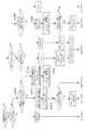
同図において、310は外部アクセスブロックアドレスAX<11:8>とインクリメントリフレッシュブロックカウンタアドレス(第1のリフレッシュブロックカウンタアドレス)AXU<3:0>とを比較する外部アドレス−UPカウンタ比較器(CMP)、320は外部アクセスブロックアドレスAX<11:8>とデクリメントリフレッシュブロックカウンタアドレス(第2のリフレッシュブロックカウンタアドレス)AXD<3:0>とを比較する外部アドレス−DOWNカウンタ比較器(CMP)、330は前記第1及び第2のリフレッシュブロックカウンタアドレス同士を比較するUP/DOWNカウンタ比較器(CMP)、340はワード線カウンタ(リフレッシュワード線カウンタ)、350はリフレッシュカウンタ制御回路(調停回路)、351はリセット付きF/F、360はインクリメントカウンタ(リフレッシュブロックカウンタ)、361はロードホールド機能付きF/F、370はデクリメントカウンタ(リフレッシュブロックカウンタ)である。 In the figure,
また、UPHITは前記比較器310の一致フラグ、DOWNHITは前記比較器320の一致フラグ、ENDCNTはリフレッシュ完了信号、CNTCKはカウンタクロック、CNTCKDは前記カウンタクロックCNTCKを遅延させた遅延カウンタクロック、ENDRFFはリフレッシュ完了フラグ、NSTOPCNTUは前記インクリメントカウンタ360の停止フラグ、NSTOPCNTDは前記デクリメントカウンタ370の停止フラグである。 UPHIT is a match flag of the
本発明では、メモリアレイ100内の全メモリブロックにおけるリフレッシュ対象のリフレッシュワード線に対して共通のワード線カウンタ340を備えていると共に、リフレッシュブロックカウンタがインクリメントカウンタ360及びデクリメントカウンタ370の2系統のカウンタによって構成されている。従って、最大で2つのメモリブロックの同時リフレッシュが可能である。また、ロウアドレスカウンタを各メモリブロック内に配置しないので、半導体記憶装置の省面積が可能である。 In the present invention, a common word line counter 340 is provided for refresh word lines to be refreshed in all memory blocks in the
さらに、リフレッシュカウンタ制御回路350を備えており、以下のように機能して、外部アクセスと内部リフレッシュとの競合を調停する。 Furthermore, a refresh counter control circuit 350 is provided, which functions as follows to arbitrate contention between external access and internal refresh.
前記インクリメントカウンタ360のアドレスAXU<3:0>若しくは前記デクリメントカウンタ370のアドレスAXD<3:0>と、外部アクセスブロックアドレスAX<11:8>とが一致する場合は、当該メモリブロックのリフレッシュアクセス及び前記インクリメントカウンタ360若しくは前記デクリメントカウンタ370のカウントアップを停止する。前記インクリメントカウンタ360のカウンタ値が前記デクリメントカウンタ370のカウンタ値よりも大きくなると、リフレッシュ動作及びカウントアップ動作を停止する。外部からリフレッシュコマンドが入力された場合には、リフレッシュ完了フラグENDCNTが立っていればリフレッシュ停止状態を保ち、立っていなければリフレッシュを実行する。 When the address AXU <3: 0> of the increment counter 360 or the address AXD <3: 0> of the decrement counter 370 matches the external access block address AX <11: 8>, refresh access of the memory block is performed. And the count-up of the increment counter 360 or the decrement counter 370 is stopped. When the counter value of the increment counter 360 becomes larger than the counter value of the decrement counter 370, the refresh operation and the count up operation are stopped. When a refresh command is input from the outside, the refresh stop state is maintained if the refresh completion flag ENDCNT is set, and refresh is executed if it is not set.
上記のいずれの場合も、外部リフレッシュコマンドサイクルの終了時に前記ワード線カウンタ340をカウントアップし、前記インクリメントカウンタ360及び前記デクリメントカウンタ370をリセットする。 In any of the above cases, the word line counter 340 is counted up at the end of the external refresh command cycle, and the increment counter 360 and the decrement counter 370 are reset.
図7は、本実施形態の半導体記憶装置におけるUP/DOWNカウンタ比較器330の全体構成の構成図を示している。 FIG. 7 is a block diagram showing the overall configuration of the UP /
同図において、インクリメントリフレッシュブロックカウンタアドレスAXU<3:0>が、デクリメントリフレッシュブロックカウンタアドレスAXD<3:0>よりも大きくなった場合に、リフレッシュ完了信号ENDCNTをイネーブルにする。 In the figure, the refresh completion signal ENDCNT is enabled when the increment refresh block counter address AXU <3: 0> becomes larger than the decrement refresh block counter address AXD <3: 0>.
図8は、本実施形態の半導体記憶装置におけるワード線カウンタ340の全体構成の構成図を示している。 FIG. 8 is a block diagram showing the overall configuration of the word line counter 340 in the semiconductor memory device of this embodiment.
同図に示したワード線カウンタ340は、一般的な8進カウンタであるので、その説明は省略する。 Since the word line counter 340 shown in the figure is a general octal counter, its description is omitted.
図9は、本実施形態の半導体記憶装置におけるロウ制御回路400の全体構成の構成図を示している。 FIG. 9 is a block diagram showing the overall configuration of the
同図において、401はR−Sラッチ、RASFはRASフラグ、RAUTFはオートリフレッシュフラグ、IRRASは内部同時リフレッシュコマンド、IRRASFはランダム・ページアクセス動作時内部RASフラグ、RFF1〜5は内部フラグである。 In the figure, 401 is an R-S latch, RASF is an RAS flag, RAUTF is an auto refresh flag, IRRAS is an internal simultaneous refresh command, IRRASF is an internal RAS flag during a random page access operation, and RFF1 to RFF5 are internal flags.
同図のロウ制御回路400では、複数サイクルにわたって外部から入力される外部RASコマンド信号NRASのイネーブル期間のクロック数をカウントし、所定の回数毎に内部同時リフレッシュコマンドIRRASを発行することで、ページ動作中の同時リフレッシュを実現する。 In the
また、前記外部RASコマンド信号NRASのディスネーブル期間のクロック数をカウントして、所定の回数毎に内部リフレッシュコマンドIRRASを発行することでプリチャージ期間中のオートリフレッシュを実現する。 In addition, the number of clocks in the disable period of the external RAS command signal NRAS is counted, and the internal refresh command IRRAS is issued every predetermined number of times to realize auto refresh during the precharge period.
上記のように構成された本実施形態の半導体記憶装置の動作を以下に示す。 The operation of the semiconductor memory device of this embodiment configured as described above will be described below.
図10は、本実施形態の半導体記憶装置における動作フローのフロー図である。 FIG. 10 is a flowchart of the operation flow in the semiconductor memory device of this embodiment.
以下、1クロックで動作が完結する仕様のDRAMの動作時の動作について説明する。 Hereinafter, an operation at the time of operation of a DRAM having a specification that the operation is completed in one clock will be described.
イニシャル状態ではインクリメントカウンタ360はブロック<0>にセットされていると共に、デクリメントカウンタ370はブロック<15>にセットされている。 In the initial state, the increment counter 360 is set in the block <0>, and the decrement counter 370 is set in the block <15>.
外部からアクセスがあったとき、そのアクセスが前記ブロック<0>又は前記ブロック<15>に対するアクセスでない場合(S1010)には、それぞれのブロックをリフレッシュする(S1011)ので、外部アクセスブロックと合わせて、16ブロック中3ブロックが同時に活性化される。 When there is an access from outside, if the access is not access to the block <0> or the block <15> (S1010), each block is refreshed (S1011). Three of the 16 blocks are activated simultaneously.
このとき、例えば、外部アクセスブロックとインクリメントカウンタ360側のリフレッシュブロックとが衝突した場合には、当該ブロックのリフレッシュは停止される。しかし、デクリメントカウンタ370側のリフレッシュブロックは外部アクセスブロックと衝突しないのでリフレッシュが可能となり(S1013)、16ブロック中2ブロックが同時に活性化される。 At this time, for example, when the external access block and the refresh block on the increment counter 360 side collide, the refresh of the block is stopped. However, since the refresh block on the decrement counter 370 side does not collide with the external access block, it can be refreshed (S1013), and two of the 16 blocks are activated simultaneously.
リフレッシュが実行できたインクリメントカウンタ360やデクリメントカウンタ370は、サイクル終了時にインクリメント若しくはデクリメントされる(S1012、S1014)。 The increment counter 360 and decrement counter 370 that have been able to be refreshed are incremented or decremented at the end of the cycle (S1012, S1014).
また、外部からのアクセスがないプリチャージ動作を検知すると(S1020)、前記インクリメントカウンタ360及びデクリメントカウンタ370の指し示すブロックを同時にリフレッシュするので(S1021)、16ブロック中2ブロックが同時に活性化される。 When a precharge operation without external access is detected (S1020), the blocks pointed to by the increment counter 360 and decrement counter 370 are refreshed simultaneously (S1021), so two of the 16 blocks are activated simultaneously.
上記のように、外部アクセスブロックとリフレッシュブロックとの衝突がなければ8サイクル後には全メモリブロックのリフレッシュが完了し、この時には、インクリメントカウンタ360のカウンタ値がデクリメントカウンタ370のカウンタ値よりも大きくなることを検知して、リフレッシュ完了フラグENDRFFを発生して以後の内部リフレッシュ動作を停止する。 As described above, if there is no collision between the external access block and the refresh block, refresh of all memory blocks is completed after 8 cycles. At this time, the counter value of the increment counter 360 becomes larger than the counter value of the decrement counter 370. When this is detected, a refresh completion flag ENDRFFF is generated and the subsequent internal refresh operation is stopped.
また、外部アクセスブロックと内部リフレッシュブロックとの競合が続いたワーストケースの場合でも、15サイクル後には外部アクセスブロックと競合する1ブロックを除いてリフレッシュが完了した状態となる。 Even in the worst case in which the competition between the external access block and the internal refresh block continues, after 15 cycles, the refresh is completed except for one block that competes with the external access block.
つまり、前記インクリメントカウンタ360及びデクリメントカウンタ370の共通のブロックアドレスとして、未リフレッシュブロックのアドレスが記憶され、当該ブロックのリフレッシュを外部からのオートリフレッシュサイクルで実施することによって、全ブロックのリフレッシュを保障することが可能となる。 That is, the address of the unrefreshed block is stored as a common block address of the increment counter 360 and the decrement counter 370, and the refresh of all the blocks is ensured by performing the refresh of the block in the auto-refresh cycle from the outside. It becomes possible.
この外部リフレッシュは所定の期間で入力され、リフレッシュ完了フラグENDRFFがイネーブルであればリフレッシュ停止状態を保ち、ディスネーブルであればリフレッシュを実行する。いずれの場合も外部リフレッシュコマンドサイクルの終了時にワード線カウンタ340をカウントアップし、インクリメントカウンタ360、デクリメントカウンタ370をリセットする。 This external refresh is input for a predetermined period. If the refresh completion flag ENDRFFF is enabled, the refresh stop state is maintained, and if disabled, the refresh is executed. In either case, the word line counter 340 is counted up at the end of the external refresh command cycle, and the increment counter 360 and the decrement counter 370 are reset.
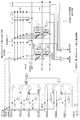
図11(A)及び同図(B)は、本実施形態の半導体記憶装置における動作タイミングのダイアグラム図であり、図12(A)及び同図(B)は、本実施形態の半導体記憶装置における他の動作タイミングのダイアグラム図である。 11A and 11B are diagrams of operation timings in the semiconductor memory device of this embodiment. FIGS. 12A and 12B are diagrams in the semiconductor memory device of this embodiment. It is a diagram of another operation timing.
以下、2クロック以上で1サイクルが完結するページ動作機能を有する仕様のDRAMの動作について説明する。 The operation of a DRAM having a specification having a page operation function that completes one cycle at two clocks or more will be described below.
図11及び図12は、1クロック目でRAS動作、2クロック目でCAS及びプリチャージを行い、2サイクルでランダム動作が完了するページ機能付き仕様のDRAM動作の動作タイミングのダイアグラムを示している。 FIG. 11 and FIG. 12 are diagrams showing the operation timing of the DRAM operation with the page function specification in which the RAS operation is performed at the first clock, the CAS and the precharge are performed at the second clock, and the random operation is completed in two cycles.
同図において、t0〜t2はランダムアクセス、t2〜5はページ長2のアクセス、t5〜9はページ長3のアクセス、t9〜14はページ長4のアクセス、t14〜16はランダムアクセス、t16〜t18はプリチャージサイクル、t18〜t20はランダムサイクル、t20〜t22はオートリフレッシュサイクルである。 In the figure, t0 to t2 are random access, t2 to 5 are
図11に示したダイアグラム図では、ページ動作の外部アクセス中及びプリチャージ期間であっても、内部リフレッシュが外部アクセスと衝突することなく実施されている。そして、t16〜t18において、プリチャージサイクル中のリフレッシュ終了後に、前記インクリメントカウンタ360のアドレスAXU<3:0>が前記デクリメントカウンタ370のアドレスAXD<3:0>よりも大きくなったことを検知して、リフレッシュ完了信号ENDCNTがイネーブルとなり、それ以降のリフレッシュを停止している。その後、t20〜22の外部オートリフレッシュサイクル後に、前記ワード線カウンタ340をカウントアップし、前記インクリメントカウンタ360、デクリメントカウンタ370をリセットしている。 In the diagram shown in FIG. 11, the internal refresh is performed without colliding with the external access even during the external access of the page operation and the precharge period. From t16 to t18, after completion of the refresh in the precharge cycle, it is detected that the address AXU <3: 0> of the increment counter 360 is larger than the address AXD <3: 0> of the decrement counter 370. Thus, the refresh completion signal ENDCNT is enabled and the subsequent refresh is stopped. Thereafter, after the external auto refresh cycle from t20 to 22, the word line counter 340 is counted up, and the increment counter 360 and the decrement counter 370 are reset.
上記のように、本発明では、全メモリブロックのリフレッシュが完了した後に内部リフレッシュ動作が停止するので、必要以上の内部リフレッシュが実施されずに消費電力の低減が可能である。 As described above, according to the present invention, since the internal refresh operation is stopped after the refresh of all the memory blocks is completed, it is possible to reduce power consumption without performing unnecessary internal refresh.
図12に示したダイアグラム図は、図11に対して、t14〜22における外部入力アドレスが異なり、t14〜16及びt18〜22においてインクリメントカウンタ360が指し示すブロックアドレスに基づく内部リフレッシュメモリブロックと外部アクセスブロックとが衝突している。そのため、t14〜16では、UPHITが「High」、NSTOPCNTUが「Low」、STOPRFUが「High」となって、インクリメントカウンタ360が指し示すブロックアドレスに基づく内部リフレッシュは停止し、カウンタのインクリメントも行われない。その後のt16〜18のサイクルは、プリチャージサイクルであるのでUPHITやDOWNHITに関わらず、両ブロックカウンタの指し示すブロックで内部リフレッシュが実施され、同サイクル終了時点のカウントアップでブロック<7>以外のメモリブロックのリフレッシュは完了状態となる。 The diagram shown in FIG. 12 differs from FIG. 11 in that the external input address at t14-22 is different and the internal refresh memory block and the external access block based on the block address indicated by the increment counter 360 at t14-16 and t18-22 And clash. Therefore, at t14 to 16, UPHIT is “High”, NSTOPCNTU is “Low”, and STOPRFU is “High”, and the internal refresh based on the block address indicated by the increment counter 360 is stopped, and the counter is not incremented. . Since the subsequent cycles from t16 to 18 are precharge cycles, regardless of UPHIT and DOWNNHIT, internal refresh is performed in the block indicated by both block counters, and the memory other than block <7> is counted up at the end of the cycle. The block refresh is completed.
また、t18〜20のサイクルでは、上記ブロック<7>が外部アクセスと衝突しているためにリフレッシュが実施されない。t20〜22のサイクルは外部オートリフレッシュサイクルであるので、強制的にSTOPRFU/STOPRFDを「Low」として未リフレッシュブロック<7>のリフレッシュを実施している。 In the cycle from t18 to 20, since the block <7> collides with external access, no refresh is performed. Since the cycle from t20 to 22 is an external auto-refresh cycle, the refresh of the unrefreshed block <7> is forcibly set to STOPRFU / STOPRFD as “Low”.
上記の外部オートリフレッシュサイクル後には、ワード線カウンタ340をカウントアップし、インクリメントカウンタ360、デクリメントカウンタ370をリセットしている。 After the external auto-refresh cycle, the word line counter 340 is counted up and the increment counter 360 and the decrement counter 370 are reset.
上記のように本実施形態では、内部リフレッシュブロックと外部アクセスブロックとが衝突し続けた場合であっても、一回のオートリフレッシュアクセスを外部から発行すれば、そのサイクルで確実にすべてのメモリブロックのリフレッシュは完了する。つまり、外部からは「メモリブロック数−1」の数だけ内部リフレッシュが実行される周期よりも長い所定の周期でオートリフレッシュコマンドを入力さえすれば、内部アドレスを管理することなく、容易にセル電荷保持時間内での全メモリセルのリフレッシュを保障する同時リフレッシュが実行可能である。例えば、電荷保持時間1msでワード線が4096本のDRAMをリフレッシュすることを考えると、従来の外部からのオートリフレッシュコマンドの入力頻度は、4096本のワード線を同時にリフレッシュすると仮定するならば、977nsに一回のリフレッシュが必要となる。一方、本発明の同時リフレッシュ手法を用いると、「4096本=256本×16ブロック」の場合には、3906nsに1回の外部からのオートリフレッシュコマンドの入力によって全メモリセルのリフレッシュを保障できる。 As described above, in the present embodiment, even if the internal refresh block and the external access block continue to collide, if one auto-refresh access is issued from the outside, all the memory blocks are surely in that cycle. The refresh is complete. That is, if the auto refresh command is input from the outside in a predetermined cycle longer than the cycle in which the internal refresh is performed by the number of “memory blocks −1”, the cell charge can be easily performed without managing the internal address. Simultaneous refresh that ensures refresh of all memory cells within the retention time can be performed. For example, considering that a DRAM having 4096 word lines is refreshed with a charge holding time of 1 ms, the conventional input frequency of an auto-refresh command is assumed to be 977 ns if it is assumed that 4096 word lines are refreshed simultaneously. One refresh is required. On the other hand, when the simultaneous refresh method of the present invention is used, in the case of “4096 lines = 256 lines × 16 blocks”, refresh of all memory cells can be ensured by inputting an auto-refresh command once every 3906 ns.
本実施形態の構成の場合には、上記リフレッシュ周期内(電荷保持時間内)で15サイクルのランダム動作が行われる必要があるが、ランダムサイクルが260nsよりも高速であればこれを満足できる。つまり、外部からのリフレッシュコマンドの入力頻度を下げることが可能であるのでシステムパフォーマンスの向上ができる。 In the case of the configuration of the present embodiment, it is necessary to perform a random operation of 15 cycles within the refresh cycle (within the charge retention time), which can be satisfied if the random cycle is faster than 260 ns. That is, since the frequency of external refresh command input can be reduced, system performance can be improved.
また、上記所定の周期でのオートリフレッシュコマンドの入力時に、多くとも1つのメモリブロック以外のリフレッシュが完了していることを保障するために、電源立ち上げ後、又はセルフリフレッシュからの復帰後の通常動作開始のサイクル(図11、12のt0〜t2のサイクルに相当)の直前のサイクルで1サイクルのダミーオートリフレッシュの実施が望ましい。 In addition, when an auto-refresh command is input at the predetermined cycle, in order to ensure that refreshing of at most one memory block has been completed, the normal operation after power-on or after returning from self-refreshing is performed. It is desirable to perform one cycle of dummy auto-refresh in the cycle immediately before the operation start cycle (corresponding to the cycle from t0 to t2 in FIGS. 11 and 12).
また、様々なページ長のページ動作中の内部リフレッシュ、及びプリチャージ動作中の内部リフレッシュを実施するためには、プリチャージサイクル中のクロック数に制限が必要である。つまり、上記構成ではリフレッシュは2クロックで完了するが、少なくともリフレッシュの第1クロックのタイミングと、外部アクセスの第1クロックのタイミングが一致する必要があるので、外部アクセス動作でCAS及びプリチャージを行うサイクルも含めたプリチャージ期間のクロック数は奇数である必要がある。 Further, in order to perform internal refresh during page operations of various page lengths and internal refresh during precharge operations, it is necessary to limit the number of clocks during the precharge cycle. In other words, in the above configuration, refresh is completed in two clocks, but at least the timing of the first clock of refresh and the timing of the first clock of external access must match, so CAS and precharge are performed in the external access operation. The number of clocks in the precharge period including the cycle needs to be an odd number.
(第2の実施形態)
以下、本発明の第2の実施形態の半導体記憶装置について、図面を参照しながら説明する。(Second Embodiment)
The semiconductor memory device according to the second embodiment of the present invention will be described below with reference to the drawings.
本実施形態の半導体記憶装置が上記第1の実施形態の半導体記憶装置と異なる点は、ロウ制御回路400の代わりにロウ制御回路1400を備えている点のみである。その他の構成については、上記第1の実施形態と同様であるので、その図示及び説明は省略する。 The semiconductor memory device of this embodiment is different from the semiconductor memory device of the first embodiment only in that a row control circuit 1400 is provided instead of the
図13は、本発明の第2の実施形態の半導体記憶装置におけるロウ制御回路1400の全体構成の構成図を示している。 FIG. 13 is a block diagram showing the overall configuration of the row control circuit 1400 in the semiconductor memory device according to the second embodiment of the present invention.
同図において、1401、1402はリセット付きF/F、1403は4入力OR素子である。 In the figure, 1401 and 1402 are reset F / Fs, 1403 is a 4-input OR element.
本実施形態のロウ制御回路1400は、上記第1の実施形態の半導体記憶装置におけるロウ制御回路400に対して、リセット付きF/F1401、1402の出力、RASフラグRASF、及び内部フラグRFF1が4入力OR素子1403に入力され、その出力として内部フラグRFF2が構成されていることを特徴としている。 The row control circuit 1400 of the present embodiment has four inputs for the outputs of the F /
図14は、本実施形態の半導体記憶装置における動作タイミングのダイアグラム図を示している。 FIG. 14 shows a diagram of operation timing in the semiconductor memory device of this embodiment.
同図において、t0〜t2はランダムアクセス、t2〜5はページ長2のアクセス、t5〜9はページ長3のアクセス、t9〜14はページ長4のアクセス、t14〜15はプリチャージサイクル、t15〜17はランダムサイクル、t17〜t21はプリチャージサイクル、t20〜t22はオートリフレッシュサイクルである。 In the figure, t0 to t2 are random accesses, t2 to 5 are
図14と図11、12とを比較すると、直前のCAS/プリチャージサイクルを含めて2クロックのプリチャージ期間で内部リフレッシュ動作を停止する機能が追加されており、プリチャージ期間中のクロック数が4クロック以上となる場合に限って偶数回のプリチャージが禁止される。 Comparing FIG. 14 with FIGS. 11 and 12, a function for stopping the internal refresh operation in the precharge period of 2 clocks including the immediately preceding CAS / precharge cycle is added, and the number of clocks during the precharge period is increased. Even when the number of clocks is four or more, even-numbered precharging is prohibited.
上記のように、本実施形態では、当該半導体記憶装置が搭載されるシステム側はプリチャージ期間でのクロック数を3クロック以内であれば管理する必要が無くなり、システム設計を容易にできる。尚、ロウ制御回路の設計次第では、システム側が管理すべきプリチャージ期間のクロック数は任意に変更可能である。 As described above, in this embodiment, the system side on which the semiconductor memory device is mounted does not need to manage if the number of clocks in the precharge period is within 3 clocks, and the system design can be facilitated. Depending on the design of the row control circuit, the number of clocks in the precharge period to be managed by the system can be arbitrarily changed.
(第3の実施形態)
以下、本発明の第3の実施形態の半導体記憶装置について、図面を参照しながら説明する。(Third embodiment)
A semiconductor memory device according to the third embodiment of the present invention will be described below with reference to the drawings.
本実施形態の半導体記憶装置が上記第1の実施形態の半導体記憶装置と異なる点は、リフレッシュカウンタ300及びロウ制御回路400の代わりにリフレッシュカウンタ2300及びロウ制御回路2400を備えている点のみである。その他の構成については、上記第1の実施形態と同様であるので、その図示及び説明は省略する。 The semiconductor memory device of this embodiment is different from the semiconductor memory device of the first embodiment only in that a
図15は、本発明の第3の実施形態の半導体記憶装置におけるリフレッシュカウンタ2300の全体構成の構成図を示している。 FIG. 15 is a block diagram showing the overall configuration of the
同図において、2351、2352、2353はセレクタ、2354、2355はOR素子、SLFFはセルフリフレッシュフラグ、NCはワード線カウンタのキャリー出力(負論理)である。 In the figure, 2351, 2352 and 2353 are selectors, 2354 and 2355 are OR elements, SLFF is a self-refresh flag, and NC is a carry output (negative logic) of a word line counter.
本実施形態のリフレッシュカウンタ2300は、上記第1の実施形態の半導体記憶装置におけるリフレッシュカウンタ300に対して、リフレッシュカウンタ制御回路350が別構成のリフレッシュカウンタ制御回路2350に置き換わった構成となっている。また、インクリメントカウンタ360及びデクリメントカウンタ370が、インクリメントカウンタ2360及びデクリメントカウンタ2370に置き換わっている。 The
図16は、本実施形態の半導体記憶装置におけるロウ制御回路2400の全体構成の構成図を示している。 FIG. 16 is a block diagram showing the overall configuration of the row control circuit 2400 in the semiconductor memory device of this embodiment.
本実施形態のロウ制御回路2400は、上記第1の実施形態の半導体記憶装置におけるロウ制御回路400に対して、外部セルフリフレッシュコマンドNRSLFの入力を受けて、セルフリフレッシュフラグSLFFを発生し、セルフ発振周波数発生回路2401でセルフリフレッシュ発振周波数を発生して、その出力をR−S F/F2402を用いてカウンタセレクト信号CNTSELを発生する回路が追加されている。 The row control circuit 2400 of the present embodiment receives an external self-refresh command NRSLF to the
本実施形態では、セルフリフレッシュモードになるとセルフリフレッシュフラグSLFFがイネーブルとなり、ワード線カウンタ340のクロックとして、セルフリフレッシュ動作時にセルフ発振周期で動作するカウンタクロックCNTCKが選択される。それと同時に、インクリメントカウンタ2360及びデクリメントカウンタ2370の初段のカウンタのロードホールドポートにワード線カウンタ340のキャリー出力NCの反転論理が入力される。また、リフレッシュ停止信号STOPRFU及びSTOPRFDも強制的にディスネーブルにされる。 In the present embodiment, when the self-refresh mode is entered, the self-refresh flag SLFF is enabled, and the counter clock CNTCK that operates in the self-oscillation period during the self-refresh operation is selected as the clock for the word line counter 340. At the same time, the inverted logic of the carry output NC of the word line counter 340 is input to the load hold ports of the first-stage counters of the increment counter 2360 and the
従って、セルフ発振周期でワード線カウンタ340とインクリメントカウンタ360及びデクリメントカウンタ370とが、連続的に接続された2系統の12進カウンタとして動作し、2ブロックが同時活性かされてリフレッシュされる。つまり、通常動作時は外部から周期的に入力される外部オートリフレッシュコマンドをトリガとして、前記ワード線カウンタ340のカウントアップや、前記インクリメントカウンタ360及びデクリメントカウンタ370のリセットを実施していたが、本構成を用いると、前記外部オートリフレッシュコマンドの入力が行われないセルフリフレッシュ動作時であっても、全ワード線アドレスのリフレッシュを自動的に実施することができる。 Accordingly, the word line counter 340, the increment counter 360, and the decrement counter 370 operate as two serially connected decimal counters in the self-oscillation cycle, and the two blocks are simultaneously activated and refreshed. That is, during normal operation, the word line counter 340 is counted up and the increment counter 360 and the decrement counter 370 are reset using an external auto-refresh command periodically input from the outside as a trigger. When the configuration is used, all word line addresses can be automatically refreshed even during a self-refresh operation in which no external auto-refresh command is input.
さらに、前記インクリメントカウンタ360及びデクリメントカウンタ370のカウンタリセット回路は、通常同時リフレッシュ動作時と同じ回路を用いることができるため、面積オーバーヘッドも最小にできる。 Further, the counter reset circuit of the increment counter 360 and the decrement counter 370 can use the same circuit as that in the normal simultaneous refresh operation, so that the area overhead can be minimized.
(第4の実施形態)
以下、本発明の第4の実施形態の半導体記憶装置について、図面を参照しながら説明する。(Fourth embodiment)
The semiconductor memory device according to the fourth embodiment of the present invention will be described below with reference to the drawings.
本実施形態の半導体記憶装置が上記第1の実施形態の半導体記憶装置と異なる点は、リフレッシュカウンタ300の代わりにリフレッシュカウンタ3300を備えている点のみである。その他の構成については、上記第1の実施形態と同様であるので、その図示及び説明は省略する。 The semiconductor memory device of this embodiment is different from the semiconductor memory device of the first embodiment only in that a
図17は、本発明の第4の実施形態の半導体記憶装置におけるリフレッシュカウンタ3300の全体構成の構成図を示している。 FIG. 17 is a block diagram showing the overall configuration of the
本実施形態のリフレッシュカウンタ3300は、上記第3の実施形態の半導体記憶装置におけるリフレッシュカウンタ2300に対して、インバータ素子3351、NOR素子3352、カウンタ制御切り替え信号CONVRFが追加された構成となっている。 The
本実施形態では、テストモード時やシステム側からの制御によってカウンタ制御切り替え信号CONVRFを制御することで、内部リフレッシュカウンタ動作を同時リフレッシュ動作から従来のセルフリフレッシュモード時と同様のカウンタ制御に切り替えることが可能となる。 In the present embodiment, the internal refresh counter operation can be switched from the simultaneous refresh operation to the same counter control as in the conventional self-refresh mode by controlling the counter control switching signal CONVRF in the test mode or by control from the system side. It becomes possible.
(第5の実施形態)
以下、本発明の第5の実施形態の半導体記憶装置について、図面を参照しながら説明する。(Fifth embodiment)
Hereinafter, a semiconductor memory device according to a fifth embodiment of the present invention will be described with reference to the drawings.
本実施形態の半導体記憶装置が上記第1の実施形態の半導体記憶装置を異なる点は、リフレッシュカウンタ300の代わりにリフレッシュカウンタ4300を備えている点のみである。その他の構成については、上記第1の実施形態と同様であるので、その図示及び説明は省略する。 The semiconductor memory device of this embodiment differs from the semiconductor memory device of the first embodiment only in that a refresh counter 4300 is provided instead of the
図18は、本発明の第5の実施形態の半導体記憶装置におけるリフレッシュカウンタ4300の全体構成の構成図を示している。 FIG. 18 is a block diagram showing the overall configuration of the refresh counter 4300 in the semiconductor memory device according to the fifth embodiment of the present invention.
同図において、4350はリフレッシュカウンタ制御回路、4380は外部アドレスAX<7:0>とワード線カウンタアドレスAXI<7:0>との比較を行う外部アドレス−WLカウンタ比較器(CMP)、4390はアクセス履歴検出回路、WLHITは前記比較器4380の一致フラグ、UPSKIPは第1のリフレッシュスキップ信号、DOWNSKIPは第2のリフレッシュスキップ信号である。 In the figure, 4350 is a refresh counter control circuit, 4380 is an external address-WL counter comparator (CMP) for comparing the external address AX <7: 0> with the word line counter address AXI <7: 0>, and 4390 is An access history detection circuit, WLHIT is a match flag of the comparator 4380, UPSKIP is a first refresh skip signal, and DOWNSKIP is a second refresh skip signal.
図19は、本実施形態のリフレッシュカウンタ4300におけるアクセス履歴検出回路4390の全体構成の構成図を示している。 FIG. 19 is a block diagram showing the overall configuration of the access
同図において、4391は第1のリフレッシュワード線ヒット検出回路、4392は第2のリフレッシュワード線ヒット検出回路、4393は4ビット分のF/F、4394は1ビットのF/F、4395は比較器(CMP)、RFHITFはリフレッシュワード線ヒット検出回路のヒットフラグである。 In the figure, 4391 is a first refresh word line hit detection circuit, 4392 is a second refresh word line hit detection circuit, 4393 is a 4-bit F / F, 4394 is a 1-bit F / F, and 4395 is a comparison. The devices (CMP) and RFHITF are hit flags of the refresh word line hit detection circuit.
図20は、本実施形態の半導体記憶装置における動作フローのフロー図である。 FIG. 20 is a flowchart of the operation flow in the semiconductor memory device of this embodiment.
本実施形態では、外部アクセスワード線アドレスAX<7:0>とリフレッシュワード線アドレスAXI<7:0>とが一致し、かつ外部アクセスブロックアドレスAX<11:8>がインクリメントリフレッシュブロックカウンタアドレスAXU<3:0>よりも小さく、かつデクリメントカウンタアドレスAXD<3:0>よりも大きな場合に限って、リフレッシュワード線ヒットフラグRFHITFがイネーブルとなる。 In this embodiment, the external access word line address AX <7: 0> matches the refresh word line address AXI <7: 0>, and the external access block address AX <11: 8> is incremented refresh block counter address AXU. The refresh word line hit flag RFHITF is enabled only when it is smaller than <3: 0> and larger than the decrement counter address AXD <3: 0>.
前記リフレッシュワード線ヒットフラグRFHITFがイネーブルになることは、現サイクル以降で、かつ次のオートリフレッシュサイクルの間で、内部リフレッシュを実行する予定のワード線が外部アクセスされたことを意味している。 When the refresh word line hit flag RFHITF is enabled, it means that the word line scheduled to execute the internal refresh is accessed externally after the current cycle and during the next auto-refresh cycle.
前記リフレッシュワード線ヒットフラグRFHITFがイネーブルとなった場合、現サイクルでの外部アクセスブロックアドレスと、内部インクリメントカウンタアドレスAXU<3:0>及びデクリメントカウンタアドレスAXD<3:0>のいずれかとが一致した場合は、第1又は第2のリフレッシュスキップ信号UPSKIP、DOWNSKIPがイネーブルとなる。前記第1又は第2のリフレッシュスキップ信号UPSKIP、DOWNSKIPがイネーブルとなると、インクリメントリフレッシュブロックカウンタアドレスリフレッシュ停止信号STOPPFU、デクリメントリフレッシュブロックカウンタアドレスリフレッシュ停止信号STOPRFDの何れかがイネーブルとなり、当該ブロックのリフレッシュが停止し、同時に当該ブロックのインクリメントカウンタ停止フラグNSTOPCNTU若しくはデクリメントカウンタ停止フラグNSTOPCNTDが強制的にディスネーブルとなるので、当該リフレッシュカウンタはカウントアップされるので結果として当該ブロックのリフレッシュがスキップされる。 When the refresh word line hit flag RFHITF is enabled, the external access block address in the current cycle matches either the internal increment counter address AXU <3: 0> or the decrement counter address AXD <3: 0>. In this case, the first or second refresh skip signals UPSKIP and DOWNSKIP are enabled. When the first or second refresh skip signal UPSKIP or DOWNSKIP is enabled, either the increment refresh block counter address refresh stop signal STOPPFU or the decrement refresh block counter address refresh stop signal STOPRFD is enabled, and the refresh of the block is stopped. At the same time, since the increment counter stop flag NSTOPCNTU or the decrement counter stop flag NSTOPCNTD of the block is forcibly disabled, the refresh counter is counted up, so that the refresh of the block is skipped as a result.
外部からオートリフレッシュコマンドが入力される間の外部アクセスブロックアドレス及びヒットフラグRFHITFは、それぞれサイクル毎に4ビット分のF/F4393及び1ビットのF/F4394に順に記憶されて、それらすべてと現リフレッシュサイクルのアクセスブロックが同時に参照・比較されて、当該リフレッシュのスキップ判定を行う。 The external access block address and the hit flag RFHITF while the auto-refresh command is input from the outside are sequentially stored in the 4-bit F /
上記のように、本実施形態では、リフレッシュを予定していたワード線が先に外部アクセスされた場合には、当該ワード線がリフレッシュされたのと等価であるので、リフレッシュをスキップして不必要なリフレッシュによる消費電力増大を抑制することができる。 As described above, in this embodiment, when a word line that is scheduled to be refreshed is accessed externally first, it is equivalent to the word line being refreshed. An increase in power consumption due to a refresh can be suppressed.
(第6の実施形態)
以下、本発明の第6の実施形態の半導体記憶装置について、図面を参照しながら説明する。(Sixth embodiment)
Hereinafter, a semiconductor memory device according to a sixth embodiment of the present invention will be described with reference to the drawings.
本実施形態の半導体記憶装置が上記第1の実施形態の半導体記憶装置を異なる点は、リフレッシュブロックセレクタ260及びリフレッシュカウンタ300の代わりに、リフレッシュブロックセレクタ5260及びリフレッシュカウンタ5300を備えている点のみである。その他の構成については、上記第1の実施形態と同様であるので、その図示及び説明は省略する。 The semiconductor memory device of this embodiment is different from the semiconductor memory device of the first embodiment only in that a
図21は、本発明の第6の実施形態の半導体記憶装置におけるリフレッシュブロックセレクタ5260の全体構成の構成図を示している。 FIG. 21 is a block diagram showing the overall configuration of the
本実施形態のリフレッシュカウンタ5260は、上記第1の実施形態の半導体記憶装置におけるリフレッシュブロックセレクタ260に対して、異なる2系統のリフレッシュブロックカウンタによってXBK_R<15:0>が生成される点が異なっている。すなわち、第1のインクリメントリフレッシュブロックカウンタアドレスAXU0<11:8>をプリデコードした第1のインクリメントブロックカウンタのリフレッシュブロックプリデコード信号XBKU0<15:0>と、第1のデクリメントリフレッシュブロックカウンタアドレスAXD0<11:8>をプリデコードした第1のデクリメントブロックカウンタのリフレッシュブロックプリデコード信号XBKD0<15:0>との論理和をリフレッシュブロック選択信号XBK_R<7:0>として生成する。 The
同様に、第2のインクリメントリフレッシュブロックカウンタアドレスAXU1<11:8>をプリデコードした第2のインクリメントブロックカウンタのリフレッシュブロックプリデコード信号XBKU1<15:0>と、第2のデクリメントリフレッシュブロックカウンタアドレスAXD1<11:8>をプリデコードした第2のデクリメントブロックカウンタのリフレッシュブロックプリデコード信号XBKD1<15:0>との論理和をリフレッシュブロック選択信号XBK_R<15:8>として生成する。そして、リフレッシュブロック選択信号XBK_R<7:0>、XBK_R<15:8>のそれぞれのイネーブルが第1及び第2のインクリメントリフレッシュブロックカウンタアドレス停止信号STOPRFU0、STOPRFU0、第1及び第2のデクリメントリフレッシュブロックカウンタアドレスリフレッシュ停止信号STOPRFD0、STOPRFD1によって制御される。 Similarly, the refresh block predecode signal XBKU1 <15: 0> of the second increment block counter obtained by predecoding the second increment refresh block counter address AXU1 <11: 8> and the second decrement refresh block counter address AXD1 A logical sum with the refresh block predecode signal XBKD1 <15: 0> of the second decrement block counter obtained by predecoding <11: 8> is generated as the refresh block selection signal XBK_R <15: 8>. The refresh block selection signals XBK_R <7: 0> and XBK_R <15: 8> are enabled by the first and second increment refresh block counter address stop signals STOPRFFU0, STOPRFFU0, the first and second decrement refresh blocks. It is controlled by counter address refresh stop signals STOPRFD0 and STOPRFD1.
図22は、本実施形態の半導体記憶装置におけるリフレッシュカウンタ5300の全体構成の構成図を示している。 FIG. 22 is a block diagram showing the overall configuration of the refresh counter 5300 in the semiconductor memory device of this embodiment.
本実施形態のリフレッシュカウンタ5300は、上記第4の実施形態における半導体記憶装置のリフレッシュカウンタ3300に対して、それぞれ独立に制御される2対のインクリメントブロックカウンタとデクリメントブロックカウンタとによって構成されている点が異なる。すなわち、第1のリフレッシュカウンタ制御回路5350iと第1のアドレス比較ブロック5390iとによって、3進の第1のインクリメントカウンタ5360i及びデクリメントカウンタ5370iが制御される。同様に、第2のリフレッシュカウンタ制御回路5350jと第1のアドレス比較ブロック5390jとによって、3進の第2のインクリメントカウンタ5360j及びデクリメントカウンタ5370jが制御される構成である。 The refresh counter 5300 of the present embodiment is composed of two pairs of increment block counters and decrement block counters that are controlled independently of the
同図において、ENDRFF0、ENDRFF1は第1及び第2のリフレッシュ完了フラグ、NSTOPCNTU0、NSTOPCNTU1は第1及び第2のインクリメントカウンタ停止フラグ、NSTOPCNTD0、NSTOPCNTD1は第1及び第2のデクリメントカウンタ停止フラグである。 In the figure, ENDRFF0 and ENDRFF1 are first and second refresh completion flags, NSTOPCNTU0 and NSTOPCNTU1 are first and second increment counter stop flags, and NSTOPCNTD0 and NSTOPCNTD1 are first and second decrement counter stop flags.
本実施形態では、上記第1〜第5の実施形態と同様の制御によって、外部アクセスブロックと内部リフレッシュメモリブロックとが衝突しないように調停しながら、最大4ブロックの同時内部リフレッシュが実行可能となる。例えば、電荷保持時間1msでワード線が4096本(4096WL=256WL×16ブロックの場合)のDRAMをリフレッシュすることを考える。この場合、上記第1〜第5の実施形態では、3906nsに1回の外部からのオートリフレッシュコマンド入力が必要であり、かつ上記リフレッシュ周期内(電荷保持時間内)で15サイクルのランダム動作が必要であるので、ランダムサイクルが260nsよりも低速な動作が許されない。一方、本実施形態では、同一リフレッシュ周期内で最悪で7サイクルのランダム動作を行うことができれば良いので、ランダムサイクルが558nsまで低速となっても動作が破綻しない。また、メモリブロック数が倍の32ブロックと多い構成となっても、260nsのランダムサイクル速度で動作が破綻しない。 In the present embodiment, simultaneous internal refresh of up to four blocks can be executed while arbitrating so that the external access block and the internal refresh memory block do not collide by the same control as in the first to fifth embodiments. . For example, consider refreshing a DRAM with 4096 word lines (in the case of 4096 WL = 256 WL × 16 blocks) with a charge retention time of 1 ms. In this case, in the first to fifth embodiments, an auto-refresh command input from the outside is required once every 3906 ns, and 15 cycles of random operation are required within the refresh cycle (within the charge holding time). Therefore, an operation whose random cycle is slower than 260 ns is not allowed. On the other hand, in the present embodiment, it is sufficient that the worst random operation of 7 cycles can be performed within the same refresh period, so that the operation does not fail even when the random cycle is slowed down to 558 ns. Even when the number of memory blocks is as large as 32 blocks, the operation does not fail at a random cycle speed of 260 ns.
(第7の実施形態)
以下、本発明の第7の実施形態の半導体記憶装置について、図面を参照しながら説明する。(Seventh embodiment)
The semiconductor memory device according to the seventh embodiment of the present invention will be described below with reference to the drawings.
本実施形態の半導体記憶装置が上記第1の実施形態の半導体記憶装置を異なる点は、リフレッシュワード線プリデコーダ250、リフレッシュブロックセレクタ260及びリフレッシュカウンタ300の代わりに、リフレッシュワード線プリデコーダ6250、リフレッシュブロックセレクタ6260及びリフレッシュカウンタ6300を備えている点のみである。その他の構成については、上記第1の実施形態と同様であるので、その図示及び説明は省略する。 The semiconductor memory device of this embodiment is different from the semiconductor memory device of the first embodiment in that instead of the refresh
図23は、本発明の第7の実施形態の半導体記憶装置におけるリフレッシュワード線プリデコーダ6250の全体構成の構成図を示している。 FIG. 23 is a block diagram showing the overall configuration of the refresh
本実施形態のリフレッシュワード線プリデコーダ6250は、リフレッシュカウンタ6300のアドレスに関わらず、2本のプリデコード信号XPW<7:0>が選択される構成となっている。 The refresh
図24は、本実施形態の半導体記憶装置におけるリフレッシュブロックセレクタ6260の全体構成の構成図を示している。 FIG. 24 is a block diagram showing the overall configuration of the
本実施形態のリフレッシュブロックセレクタ6260は、上記第1の実施形態のリフレッシュブロックセレクタ260に対して、2対のリフレッシュブロック選択信号XBK_R<15:0>に対して共通のインクリメントブロックカウンタのリフレッシュブロックプリデコード信号XBKU<15:0>及びデクリメントブロックカウンタのリフレッシュブロックプリデコード信号XBKD<15:0>が接続されている点が異なっており、同時に最大2本のリフレッシュブロック選択信号XBK_R<15:0>が選択される構成となっている。 The
図25は、本実施形態の半導体記憶装置におけるリフレッシュカウンタ6300の全体構成の構成図を示している。 FIG. 25 is a block diagram showing the overall configuration of the
本実施形態のリフレッシュカウンタ6300は、上記第4の実施形態の半導体記憶装置におけるリフレッシュカウンタ3300に対して、インクリメントブロックカウンタ6360及びデクリメントブロックカウンタ6370が3進カウンタに変更されている点が異なる。 The
本実施形態では、上記第6の実施形態と同様に、外部アクセスと内部リフレッシュメモリブロックとが衝突しないように調停しながら、最大4ブロックの同時内部リフレッシュが実行可能となり、しかも第6の実施形態よりも省面積な回路で実現することができる。 In the present embodiment, as in the sixth embodiment described above, simultaneous internal refresh of up to four blocks can be executed while arbitrating so that external access and the internal refresh memory block do not collide, and the sixth embodiment. It can be realized with a circuit having a smaller area.
尚、本発明は上記の実施形態のみに限定されるものではなく、その要旨を逸脱しない範囲において種々変更可能であることは言うまでもない。 Needless to say, the present invention is not limited to the above-described embodiment, and various modifications can be made without departing from the scope of the invention.
以上説明したように、本発明は、半導体記憶装置が搭載されるシステム側が内部リフレッシュアドレスを意識することなく、外部からのアクセスと内部リフレッシュとの同時実行が省面積・低電力で可能となるので、特に、電荷保持時間の短い半導体記憶装置やその制御方法等として有用である。 As described above, according to the present invention, the system side in which the semiconductor memory device is mounted can simultaneously execute external access and internal refresh with a small area and low power without being aware of the internal refresh address. In particular, it is useful as a semiconductor memory device having a short charge retention time, a control method thereof, and the like.
100 メモリアレイ
110 メモリブロック
120 センスアンプ列
121 センスアンプ
130 セルアレイ
131 メモリセル
132 ビット線
133 ワード線
200 ロウプリデコーダ(調停回路)
210 ブロック信号プリデコーダ
220 ワード線プリデコーダ
230、240 リフレッシュブロック信号プリデコーダ
250 リフレッシュワード線プリデコーダ
260、5260 リフレッシュブロックセレクタ
300、2300、3300、
4300、5300 リフレッシュカウンタ
310、320、330、
4380、4395 比較器
340 ワード線カウンタ(リフレッシュワード線カウンタ)
350、4350 リフレッシュカウンタ制御回路(調停回路)
351 リセット付きF/F
360 インクリメントカウンタ
(リフレッシュメモリブロックカウンタ)
361 ロードホールド機能付きF/F
370 デクリメントカウンタ
(リフレッシュメモリブロックカウンタ)
400、1400、2400 ロウ制御回路
401 R−Sラッチ
500 タイミング発生回路
600 ロウデコーダ(調停回路)
700 アドレスラッチブロック
1401、1402 リセット付きF/F
1403 4入力OR素子
2351、2352、2353 セレクタ
2354、2355 OR素子
2401 セルフ発振周波数発生回路
2402 R−S F/F
3351 インバータ素子
3352 NOR素子
4390 アクセス履歴検出回路
4391 第1のリフレッシュワード線ヒット検出回路
4392 第2のリフレッシュワード線ヒット検出回路
4393 4ビットのF/F(レジスタ)
4394 1ビットのF/F(レジスタ)
5350i 第1のリフレッシュカウンタ制御回路
5350j 第2のリフレッシュカウンタ制御回路
5360i 第1のインクリメントカウンタ
5360j 第2のインクリメントカウンタ
5370i 第1のデクリメントカウンタ
5370j 第2のデクリメントカウンタ
5390i 第1のアドレス比較ブロック
5390j 第2のアドレス比較ブロック
RDDD<11:0> 外部ロウアドレス
CLK 外部クロック
NRAS 外部RASコマンド信号
NRAUT 外部オートリフレッシュコマンド信号
NRST 外部リセット信号
AX<11:0> 外部ロウアドレスラッチ信号
AXU<11:8> インクリメント
リフレッシュブロックカウンタアドレス
AXD<11:8> デクリメント
リフレッシュブロックカウンタアドレス
AXI 内部リフレッシュワード線アドレス
STOPRFU インクリメントリフレッシュ
ブロックカウンタアドレスリフレッシュ停止信号
STOPRFD デクリメントリフレッシュ
ブロックカウンタアドレスリフレッシュ停止信号
AUTF オートリフレッシュフラグ
AUTPRCF オートリフレッシュ・プリチャージフラグ
CNTSEL カウンタセレクト信号
IRAS 内部RAS信号
XPW<3:0> ワード線プリデコード信号
XPA<7:0> ワード線プリデコード信号
XPB<7:0> ワード線プリデコード信号
XPW_R<3:0> リフレッシュワード線プリデコード信号
XPA_R<7:0> リフレッシュワード線プリデコード信号
XPB_R<7:0> リフレッシュワード線プリデコード信号
XBK<15:0> ブロック選択信号
XBK_R<15:0> リフレッシュブロック選択信号
#PREN プリチャージタイミング信号
#WLEN ワード線タイミング信号
#SEN センスアンプタイミング信号
WL<4095:0> ワード線
XBKU<15:0> インクリメントブロックカウンタ
リフレッシュブロックプリデコード信号
XBKD<15:0> デクリメントブロックカウンタ
リフレッシュブロックプリデコード信号
UPHIT 比較器310の一致フラグ
DOWNHIT 比較器320の一致フラグ
ENDCNT リフレッシュ完了信号
CNTCK カウンタクロック
CNTCKD 遅延カウンタクロック
ENDRFF リフレッシュ完了フラグ
NSTOPCNTU インクリメントカウンタ停止フラグ
NSTOPCNTD デクリメントカウンタ停止フラグ
RASF RASフラグ
RAUTF オートリフレッシュフラグ
IRRAS 内部同時リフレッシュコマンド
IRRASF ランダム・ページアクセス動作時内部RASフラグ
RFF1、RFF2、RFF3、
RFF4、RFF5 内部フラグ
SLFF セルフリフレッシュフラグ
NC ワード線カウンタのキャリー出力
NRSLF 外部セルフリフレッシュコマンド
SLFF セルフリフレッシュフラグ
CONVRF カウンタ制御切り替え信号
WLHIT 比較器4380の一致フラグ
UPSKIP 第1のリフレッシュスキップ信号
DOWNSKIP 第2のリフレッシュスキップ信号
RFHITF リフレッシュワード線ヒット検出回路の
ヒットフラグ
AXU0<11:8> 第1のインクリメント
リフレッシュブロックカウンタアドレス
AXU1<11:8> 第2のインクリメント
リフレッシュブロックカウンタアドレス
AXD0<11:8> 第1のデクリメント
リフレッシュブロックカウンタアドレス
AXD1<11:8> 第2のデクリメント
リフレッシュブロックカウンタアドレス
XBKU0<15:0> 第1のインクリメントブロックカウンタ
リフレッシュブロックプリデコード信号
XBKU1<15:0> 第2のインクリメントブロックカウンタ
リフレッシュブロックプリデコード信号
XBKD0<15:0> 第1のデクリメントブロックカウンタ
リフレッシュブロックプリデコード信号
XBKD1<15:0> 第2のデクリメントブロックカウンタ
リフレッシュブロックプリデコード信号
STOPRFU0 第1のインクリメントリフレッシュ
ブロックカウンタアドレスリフレッシュ停止信号
STOPRFU1 第2のインクリメントリフレッシュ
ブロックカウンタアドレスリフレッシュ停止信号
STOPRFU0 第1のデクリメントリフレッシュ
ブロックカウンタアドレスリフレッシュ停止信号
STOPRFU1 第2のデクリメントリフレッシュ
ブロックカウンタアドレスリフレッシュ停止信号
ENDRFF0 第1のリフレッシュ完了フラグ
ENDRFF1 第2のリフレッシュ完了フラグ
NSTOPCNTU0 第1のインクリメントカウンタ停止フラグ
NSTOPCNTU1 第2のインクリメントカウンタ停止フラグ
NSTOPCNTD0 第1のデクリメントカウンタ停止フラグ
NSTOPCNTD1 第2のデクリメントカウンタ停止フラグ100
210
4300, 5300 refresh counters 310, 320, 330,
4380, 4395 Comparator 340 Word line counter (refresh word line counter)
350, 4350 Refresh counter control circuit (arbitration circuit)
351 F / F with reset
360 Increment counter
(Refresh memory block counter)
361 F / F with load hold function
370 Decrement counter
(Refresh memory block counter)
400, 1400, 2400
700 Address latch blocks 1401 and 1402 F / F with reset
1403 4-input OR
3351
4394 1-bit F / F (register)
5350i first refresh
Refresh block counter address AXD <11: 8> Decrement
Refresh block counter address AXI Internal refresh word line address STOPRFU Increment refresh
Block counter address refresh stop signal STOPRFD Decrement refresh
Block counter address refresh stop signal AUTF Auto refresh flag AUTPRCF Auto refresh precharge flag CNTSEL Counter select signal IRAS Internal RAS signal XPW <3: 0> Word line predecode signal XPA <7: 0> Word line predecode signal XPB <7 : 0> Word line predecode signal XPW_R <3: 0> Refresh word line predecode signal XPA_R <7: 0> Refresh word line predecode signal XPB_R <7: 0> Refresh word line predecode signal XBK <15: 0> Block selection signal XBK_R <15: 0> Refresh block selection signal #PREN Precharge timing signal #WLEN Word line timing signal #SEN Sense amplifier timing signal L <4095: 0> word line XBKU <15: 0> increment block counter
Refresh block predecode signal XBKD <15: 0> Decrement block counter
Refresh block predecode signal UPHIT Comparator
RFF4, RFF5 Internal flag SLFF Self-refresh flag NC Word line counter carry output NRSLF External self-refresh command SLFF Self-refresh flag CONVRF Counter control switching signal WLHIT Comparator 4380 match flag UPSKIP First refresh skip signal DOWNSKIP Second refresh skip Signal RFHITF Refresh word line hit detection circuit
Hit flag AXU0 <11: 8> First increment
Refresh block counter address AXU1 <11: 8> Second increment
Refresh block counter address AXD0 <11: 8> First decrement
Refresh block counter address AXD1 <11: 8> Second decrement
Refresh block counter address XBKU0 <15: 0> First increment block counter
Refresh block predecode signal XBKU1 <15: 0> Second increment block counter
Refresh block predecode signal XBKD0 <15: 0> First decrement block counter
Refresh block predecode signal XBKD1 <15: 0> Second decrement block counter
Refresh block predecode signal STOPRFU0 First increment refresh
Block counter address refresh stop signal STOPRFU1 Second increment refresh
Block counter address refresh stop signal STOPRFU0 First decrement refresh
Block counter address refresh stop signal STOPRFU1 Second decrement refresh
Block counter address refresh stop signal ENDRFF0 First refresh completion flag ENDRFF1 Second refresh completion flag NSTOPCNTU0 First increment counter stop flag NSTOPCNTU1 Second increment counter stop flag NSTOPCNTD0 First decrement counter stop flag NSTOPCNTD1 Second decrement counter Stop flag
Claims (35)
Translated fromJapanese2つ以上のメモリブロックのブロックアドレスを生成して、前記複数のメモリブロックのうち、リフレッシュを行う2つ以上のメモリブロックを選択する複数のリフレッシュメモリブロックカウンタと、
前記2つ以上のメモリブロックに対して共通な共通ワード線アドレスを生成するリフレッシュワード線カウンタと、
前記2つ以上のブロックアドレスと前記共通ワード線アドレスとに基づいて、少なくとも1つ以上の第1のワード線アドレスを生成し、外部から供給される第2のワード線アドレスの示すワード線に対してアクセスされる期間に、前記少なくとも1つ以上の第1のワード線アドレスの示す各々のワード線のリフレッシュを行うように調停する調停回路とを備えた
ことを特徴とする半導体記憶装置。A plurality of memory cells arranged in a matrix; a plurality of word lines each corresponding to a row of the plurality of memory cells; a plurality of bit lines each corresponding to a column of the plurality of memory cells; and the plurality of memories A plurality of sense amplifiers each corresponding to a column of cells, and among the plurality of word lines, a plurality of memory blocks in which only one word line is activated simultaneously;
A plurality of refresh memory block counters for generating block addresses of two or more memory blocks and selecting two or more memory blocks to be refreshed from among the plurality of memory blocks;
A refresh word line counter for generating a common common word line address for the two or more memory blocks;
Based on the two or more block addresses and the common word line address, at least one first word line address is generated, and the word line indicated by the second word line address supplied from the outside is generated. And an arbitration circuit that arbitrates to refresh each of the word lines indicated by the at least one first word line address during a period of access.
前記調停回路は、前記複数のリフレッシュメモリブロックカウンタで選択された2つ以上のメモリブロックのうちの何れか1つのメモリブロックと、前記第2のワード線アドレスに対応し外部からのアクセスが行われるメモリブロックとが一致するとき、当該メモリブロックのリフレッシュを停止させるように調停する
ことを特徴とする半導体記憶装置。2. The semiconductor memory device according to claim 1, wherein
The arbitration circuit is accessed from the outside corresponding to the second word line address and any one of the two or more memory blocks selected by the plurality of refresh memory block counters. Arbitration is performed so as to stop refreshing of the memory block when the memory block matches with the memory block.
前記複数のリフレッシュメモリブロックカウンタは、リフレッシュ実行後に毎回カウントアップされ、前記リフレッシュワード線カウンタは、全てのメモリブロックに対してリフレッシュが完了した後にカウントアップされる
ことを特徴とする半導体記憶装置。2. The semiconductor memory device according to claim 1, wherein
The semiconductor memory device, wherein the plurality of refresh memory block counters are counted up every time after the refresh is executed, and the refresh word line counter is counted up after the refresh is completed for all the memory blocks.
当該半導体記憶装置には、その外部から所定の周期毎にリフレッシュ要求が入力され、
前記所定の周期は、当該半導体記憶装置に備えた複数のメモリブロックのうち、リフレッシュが完了していないメモリブロックが1つ以下となる周期である
ことを特徴とする半導体記憶装置。2. The semiconductor memory device according to claim 1, wherein
A refresh request is input to the semiconductor memory device at predetermined intervals from the outside,
The predetermined cycle is a cycle in which the number of memory blocks in which refresh has not been completed among a plurality of memory blocks provided in the semiconductor storage device is one or less.
当該半導体記憶装置の外部からのリフレッシュ要求が入力されたとき、前記複数のリフレッシュメモリブロックカウンタの各々には、リフレッシュが完了していないメモリブロックのブロックアドレスが共通のアドレスとして記憶されている
ことを特徴とする半導体記憶装置。5. The semiconductor memory device according to claim 4, wherein
When a refresh request from the outside of the semiconductor memory device is input, each of the plurality of refresh memory block counters stores a block address of a memory block that has not been refreshed as a common address. A semiconductor memory device.
当該半導体記憶装置の外部からのリフレッシュ要求が入力される毎に、前記複数のリフレッシュメモリブロックカウンタがリセットされると共に、前記リフレッシュワード線カウンタがカウントアップされる
ことを特徴とする半導体記憶装置。2. The semiconductor memory device according to claim 1, wherein
Each time a refresh request is input from the outside of the semiconductor memory device, the plurality of refresh memory block counters are reset and the refresh word line counter is counted up.
当該半導体記憶装置には、電源立ち上げ後、又はセルフリフレッシュからの復帰後の通常動作開始の直前に、1回のダミー外部リフレッシュ要求が入力される
ことを特徴とする半導体記憶装置。The semiconductor memory device according to claim 6.
The semiconductor memory device is characterized in that one dummy external refresh request is input to the semiconductor memory device immediately before starting normal operation after power-on or after returning from self-refresh.
前記複数のリフレッシュメモリブロックカウンタは、リフレッシュ実行後に毎回カウントアップされ、
前記調停回路は、全てのメモリブロックに対してリフレッシュが完了した後には、次に前記リフレッシュワード線カウンタがカウントアップされるまで、内部リフレッシュ動作を停止するように調停する
ことを特徴とする半導体記憶装置。2. The semiconductor memory device according to claim 1, wherein
The plurality of refresh memory block counters are counted up every time refresh is executed,
The arbitration circuit arbitrates to stop the internal refresh operation until the refresh word line counter is counted up after the refresh is completed for all the memory blocks. apparatus.
2個のリフレッシュメモリブロックカウンタは、1対のインクリメントカウンタとデクリメントカウンタとによって構成される
ことを特徴とする半導体記憶装置。2. The semiconductor memory device according to claim 1, wherein
The two refresh memory block counters are constituted by a pair of increment counters and decrement counters.
前記調停回路は、前記インクリメントカウンタの値が前記デクリメントカウンタの値よりも大きくなった時に、全てのメモリブロックのリフレッシュが完了したことを示すフラグを発生する
ことを特徴とする半導体記憶装置。10. The semiconductor memory device according to claim 9, wherein
The arbitration circuit generates a flag indicating that the refresh of all the memory blocks is completed when the value of the increment counter becomes larger than the value of the decrement counter.
当該半導体記憶装置の外部からのリフレッシュ要求が入力されたとき、前記インクリメントカウンタの値と前記デクリメントカウンタの値とが一致する場合、前記調停回路は、前記インクリメントカウンタ及び前記デクリメントカウンタが示すメモリブロックを外部リフレッシュアクセスサイクルでリフレッシュするように調停する
ことを特徴とする半導体記憶装置。10. The semiconductor memory device according to claim 9, wherein
When a refresh request from the outside of the semiconductor memory device is input, if the value of the increment counter matches the value of the decrement counter, the arbitration circuit stores the memory block indicated by the increment counter and the decrement counter. A semiconductor memory device, wherein arbitration is performed so that refresh is performed in an external refresh access cycle.
セルフリフレッシュ時に、前記複数のリフレッシュメモリブロックカウンタは、前記リフレッシュワード線カウンタのキャリー出力信号に応じてカウントアップされるように切り替えられる
ことを特徴とする半導体記憶装置。2. The semiconductor memory device according to claim 1, wherein
In the self-refresh, the plurality of refresh memory block counters are switched so as to be counted up in accordance with a carry output signal of the refresh word line counter.
前記複数のリフレッシュメモリブロックカウンタ及び前記リフレッシュワード線カウンタの各々は、セルフリフレッシュ周期でカウントアップされる
ことを特徴とする半導体記憶装置。13. The semiconductor memory device according to claim 12, wherein
Each of the plurality of refresh memory block counters and the refresh word line counter is counted up in a self-refresh cycle.
当該半導体記憶装置の外部からの外部制御によって、前記複数のリフレッシュメモリブロックカウンタは、前記リフレッシュワード線カウンタのキャリー出力信号に応じてカウントアップされるように切り替えられる
ことを特徴とする半導体記憶装置。2. The semiconductor memory device according to claim 1, wherein
The semiconductor memory device, wherein the plurality of refresh memory block counters are switched to be counted up according to a carry output signal of the refresh word line counter by external control from the outside of the semiconductor memory device.
さらに、当該半導体記憶装置の外部から供給された前記第2のワード線アドレスの記憶手段を備え、
前記調停回路は、前記第1のワード線アドレスと、前記記憶手段に記憶された1つ以上の第2のワード線アドレスとを比較し、一致する場合は前記第1のワード線アドレスの示すワード線のリフレッシュをスキップするように調停する
ことを特徴とする半導体記憶装置。2. The semiconductor memory device according to claim 1, wherein
Furthermore, the storage means for the second word line address supplied from the outside of the semiconductor memory device,
The arbitration circuit compares the first word line address with one or more second word line addresses stored in the storage means, and if they match, the word indicated by the first word line address A semiconductor memory device, wherein arbitration is performed so as to skip line refresh.
前記記憶手段は、外部アクセスメモリブロックアドレス記憶手段と、前記第1及び第2のワード線アドレスの一致フラグ記憶手段とによって構成される
ことを特徴とする半導体記憶装置。16. The semiconductor memory device according to claim 15, wherein
The storage means comprises an external access memory block address storage means and a match flag storage means for the first and second word line addresses.
前記記憶手段は、当該半導体記憶装置の外部からリフレッシュ要求が入力される度にリセットされる
ことを特徴とする半導体記憶装置。16. The semiconductor memory device according to claim 15, wherein
The memory means is reset whenever a refresh request is input from the outside of the semiconductor memory device.
前記第1のワード線アドレスは、第1のプリデコード信号線を用いて伝送されると共に、前記第2のワード線アドレスは、第2のプリデコード信号線を用いて伝送され、
前記第1及び第2のプリデコード信号線の信号線数は同数である
ことを特徴とする半導体記憶装置。2. The semiconductor memory device according to claim 1, wherein
The first word line address is transmitted using a first predecode signal line, and the second word line address is transmitted using a second predecode signal line,
The number of signal lines of said 1st and 2nd predecode signal line is the same number. The semiconductor memory device characterized by the above-mentioned.
前記複数のリフレッシュメモリブロックカウンタは、複数対のインクリメントカウンタとデクリメントカウンタとによって構成され、
前記複数のメモリセルによって構成される複数のメモリアレイを複数の領域に分割したそれぞれの領域に対して、1対のインクリメントカウンタ及びデクリメントカウンタが割り当てられる
ことを特徴とする半導体記憶装置。2. The semiconductor memory device according to claim 1, wherein
The plurality of refresh memory block counters are constituted by a plurality of pairs of increment counters and decrement counters,
A semiconductor memory device, wherein a pair of increment counters and decrement counters are assigned to respective regions obtained by dividing the plurality of memory arrays formed of the plurality of memory cells into a plurality of regions.
前記複数のメモリブロックに共通なブロックアドレスを生成する複数のリフレッシュメモリブロックカウンタと、
前記複数のメモリブロックのうち、2つ以上のメモリブロックに対して共通な共通ワード線アドレスを生成するリフレッシュワード線カウンタと、
前記ブロックアドレスと前記共通ワード線アドレスとに基づいて、少なくとも1つ以上の第1のワード線アドレスを生成し、外部から供給される第2のワード線アドレスの示すワード線に対してアクセスされる期間に、前記少なくとも1つ以上の第1のワード線アドレスの示す各々のワード線のリフレッシュを行うように調停する調停回路とを備えた
ことを特徴とする半導体記憶装置。A plurality of memory cells arranged in a matrix; a plurality of word lines each corresponding to a row of the plurality of memory cells; a plurality of bit lines each corresponding to a column of the plurality of memory cells; and the plurality of memories A plurality of sense amplifiers each corresponding to a column of cells, and among the plurality of word lines, a plurality of memory blocks in which only one word line is activated simultaneously;
A plurality of refresh memory block counters for generating a block address common to the plurality of memory blocks;
A refresh word line counter that generates a common word line address for two or more memory blocks of the plurality of memory blocks;
At least one or more first word line addresses are generated based on the block address and the common word line address, and the word line indicated by the second word line address supplied from the outside is accessed. A semiconductor memory device comprising: an arbitration circuit that arbitrates to refresh each word line indicated by the at least one or more first word line addresses during the period.
前記調停回路は、当該半導体記憶装置の外部からアクセスされるページアクセス期間中に、前記少なくとも1つ以上の第1のワード線アドレスの示す各々のワード線のリフレッシュを行うように調停する
ことを特徴とする半導体記憶装置。In the semiconductor memory device according to any one of claims 1 to 20,
The arbitration circuit arbitrates so that each word line indicated by the at least one or more first word line addresses is refreshed during a page access period accessed from outside the semiconductor memory device. A semiconductor memory device.
さらに、ロウ制御回路を備え、
前記ロウ制御回路は、複数サイクルにわたって外部から入力されるロウアクセスコマンド信号のイネーブルクロック数をカウントし、所定の回数毎に内部同時リフレッシュコマンドを発行する
ことを特徴とする半導体記憶装置。The semiconductor memory device according to claim 21, wherein
Furthermore, a row control circuit is provided,
The row control circuit counts the number of enable clocks of a row access command signal input from the outside over a plurality of cycles, and issues an internal simultaneous refresh command every predetermined number of times.
前記調停回路は、プリチャージ期間であることを検知して、複数の第1のワード線アドレスの示すワード線の同時リフレッシュを行うように調停する
ことを特徴とする半導体記憶装置。The semiconductor memory device according to any one of claims 1 to 22,
The arbitration circuit detects a precharge period, and arbitrates so as to perform simultaneous refresh of the word lines indicated by the plurality of first word line addresses.
前記ロウ制御回路は、外部から入力されるロウアクセスコマンド信号のディスネーブルクロック数をカウントし、所定の回数毎に内部同時リフレッシュコマンドを発行する
ことを特徴とする半導体記憶装置。24. The semiconductor memory device according to claim 22 or 23.
The row control circuit counts the number of disable clocks of a row access command signal input from the outside, and issues an internal simultaneous refresh command every predetermined number of times.
当該半導体記憶装置の動作がプリチャージ期間のとき、当該半導体記憶装置に入力される入力クロック数は、所定の制限数以下である
ことを特徴とする半導体記憶装置。25. The semiconductor memory device according to claim 21, wherein:
When the operation of the semiconductor memory device is in a precharge period, the number of input clocks input to the semiconductor memory device is equal to or less than a predetermined limit number.
最小ランダムサイクルが2クロックのとき、プリチャージ期間の入力クロック数が奇数である
ことを特徴とする半導体記憶装置。26. The semiconductor memory device according to claim 25, wherein
When the minimum random cycle is 2 clocks, the number of input clocks in the precharge period is an odd number.
最小ランダムサイクルが2クロックのとき、プリチャージ期間の入力クロック数が所定の回数以上となる場合には、その入力クロック数は奇数である
ことを特徴とする半導体記憶装置。26. The semiconductor memory device according to claim 25, wherein
When the minimum random cycle is 2 clocks and the number of input clocks in the precharge period is equal to or greater than a predetermined number, the number of input clocks is an odd number.
前記複数のメモリブロックを順番に内部リフレッシュするアドレスを発生する複数のブロックカウンタの値の大小を検出する工程と、
前記工程の検出結果に基づいて、リフレッシュを一時停止する工程とを有する
ことを特徴とする内部リフレッシュ停止方法。A plurality of memory blocks each including a plurality of memory cells arranged in a matrix, a plurality of word lines, a plurality of bit lines, and a plurality of sense amplifiers are activated to activate only one word line at a time. In the internal refresh stopping method in the semiconductor memory device,
Detecting the magnitude of values of a plurality of block counters for generating addresses for internally refreshing the plurality of memory blocks in order;
And a step of temporarily stopping refreshing based on the detection result of the step.
前記複数のブロックカウンタが、1対若しくは複数対のインクリメントカウンタとデクリメントカウンタとで構成された場合に、内部リフレッシュが実行される度に前記インクリメントカウンタ及びデクリメントカウンタのカウントを行うと共に、前記インクリメントカウンタのカウンタ値及び前記デクリメントカウンタのカウンタ値の大小を比較する工程と、
前記インクリメントカウンタのカウンタ値が前記デクリメントカウンタのカウンタ値よりも大きくなった時点で内部リフレッシュを一時停止する工程とを有する
ことを特徴とする内部リフレッシュ停止方法。The internal refresh stop method according to claim 28, wherein
When the plurality of block counters are composed of one or more pairs of increment counters and decrement counters, the increment counters and decrement counters are counted each time an internal refresh is executed, and the increment counters Comparing the counter value and the magnitude of the counter value of the decrement counter;
A method of stopping internal refresh when the counter value of the increment counter becomes larger than the counter value of the decrement counter.
内部リフレッシュの一時停止の状態は、外部からのリフレッシュコマンドが発行されるまで継続される
ことを特徴とする内部リフレッシュ停止方法。The internal refresh stop method according to claim 28, wherein
The internal refresh suspension method, wherein the internal refresh pause state is continued until an external refresh command is issued.
外部アクセスされるメモリブロックと内部リフレッシュメモリブロックとの衝突を検出する工程と、
前記工程で衝突を検出したとき、内部リフレッシュ及び前記ブロックカウンタのカウントを停止する工程とを有する
ことを特徴とする外部アクセスと内部リフレッシュとの競合処理方法。A plurality of memory blocks each including a plurality of memory cells arranged in a matrix, a plurality of word lines, a plurality of bit lines, and a plurality of sense amplifiers, wherein only one of the word lines is simultaneously activated; In a conflict processing method between external access and internal refresh in a semiconductor memory device comprising a plurality of block counters for generating addresses for internally refreshing the plurality of memory blocks in order,
Detecting a collision between an externally accessed memory block and an internal refresh memory block;
A conflict processing method between external access and internal refresh, characterized in that when a collision is detected in the step, the internal refresh and the block counter are stopped.
外部アクセスされるメモリブロックと内部リフレッシュメモリブロックとの衝突が外部リフレッシュまで継続した場合、外部リフレッシュサイクルで前記衝突メモリブロックをリフレッシュする
ことを特徴とする外部アクセスと内部リフレッシュとの競合処理方法。The contention processing method between external access and internal refresh according to claim 31,
A conflict processing method between external access and internal refresh, wherein when a collision between an externally accessed memory block and an internal refresh memory block continues until external refresh, the conflict memory block is refreshed in an external refresh cycle.
外部リフレッシュコマンドの入力を検出する工程と、
前記工程で外部リフレッシュコマンドの入力を検出したとき、前記複数のブロックカウンタを初期化する工程とを有する
ことを特徴とするカウンタ初期化手法。A plurality of memory blocks each including a plurality of memory cells arranged in a matrix, a plurality of word lines, a plurality of bit lines, and a plurality of sense amplifiers, wherein only one of the word lines is simultaneously activated; In a counter initialization method in a semiconductor memory device comprising a plurality of block counters for generating addresses for internally refreshing the plurality of memory blocks in order,
Detecting the input of an external refresh command;
And a step of initializing the plurality of block counters when an input of an external refresh command is detected in the step.
外部リフレッシュサイクルを検出する工程と、
前記工程で外部リフレッシュサイクルを検出したとき、前記複数のブロックカウンタに共通するアドレスをリフレッシュする工程とを有する
ことを特徴とする外部リフレッシュのリフレッシュアドレス検出方法。A plurality of memory blocks each including a plurality of memory cells arranged in a matrix, a plurality of word lines, a plurality of bit lines, and a plurality of sense amplifiers, wherein only one of the word lines is simultaneously activated; In a refresh address detection method for external refresh in a semiconductor memory device comprising a plurality of block counters for generating addresses for internally refreshing the plurality of memory blocks in order,
Detecting an external refresh cycle; and
A refresh address detection method for external refresh, comprising: refreshing an address common to the plurality of block counters when an external refresh cycle is detected in the step.
前記複数のブロックカウンタが、1対若しくは複数対のインクリメントカウンタとデクリメントカウンタとで構成された場合に、内部リフレッシュが実行される度に前記インクリメントカウンタ及びデクリメントカウンタのカウントを行うと共に、前記インクリメントカウンタのカウンタ値及び前記デクリメントカウンタのカウンタ値の大小を比較する工程と、
前記工程において、前記インクリメントカウンタのカウンタ値と前記デクリメントカウンタのカウンタ値とが一致する場合に、外部リフレッシュを実行する工程とを有する
ことを特徴とする外部リフレッシュ実行選択方法。A plurality of memory blocks each including a plurality of memory cells arranged in a matrix, a plurality of word lines, a plurality of bit lines, and a plurality of sense amplifiers, wherein only one of the word lines is simultaneously activated; In the external refresh execution selection method in a semiconductor memory device comprising a plurality of block counters for generating addresses for internally refreshing the plurality of memory blocks in order,
When the plurality of block counters are composed of one or more pairs of increment counters and decrement counters, the increment counters and decrement counters are counted each time an internal refresh is executed, and the increment counters Comparing the counter value and the magnitude of the counter value of the decrement counter;
An external refresh execution selection method comprising the step of executing external refresh when the counter value of the increment counter matches the counter value of the decrement counter in the step.
Priority Applications (3)
| Application Number | Priority Date | Filing Date | Title |
|---|---|---|---|
| JP2007102910AJP2008262616A (en) | 2007-04-10 | 2007-04-10 | Semiconductor memory device, internal refresh stop method, contention processing method between external access and internal refresh, counter initialization method, external refresh refresh address detection method, and external refresh execution selection method |
| US12/100,271US7692993B2 (en) | 2007-04-10 | 2008-04-09 | Semiconductor memory device |
| CNA2008100921608ACN101286361A (en) | 2007-04-10 | 2008-04-10 | Semiconductor memory device |
Applications Claiming Priority (1)
| Application Number | Priority Date | Filing Date | Title |
|---|---|---|---|
| JP2007102910AJP2008262616A (en) | 2007-04-10 | 2007-04-10 | Semiconductor memory device, internal refresh stop method, contention processing method between external access and internal refresh, counter initialization method, external refresh refresh address detection method, and external refresh execution selection method |
Publications (1)
| Publication Number | Publication Date |
|---|---|
| JP2008262616Atrue JP2008262616A (en) | 2008-10-30 |
Family
ID=39853574
Family Applications (1)
| Application Number | Title | Priority Date | Filing Date |
|---|---|---|---|
| JP2007102910APendingJP2008262616A (en) | 2007-04-10 | 2007-04-10 | Semiconductor memory device, internal refresh stop method, contention processing method between external access and internal refresh, counter initialization method, external refresh refresh address detection method, and external refresh execution selection method |
Country Status (3)
| Country | Link |
|---|---|
| US (1) | US7692993B2 (en) |
| JP (1) | JP2008262616A (en) |
| CN (1) | CN101286361A (en) |
Families Citing this family (64)
| Publication number | Priority date | Publication date | Assignee | Title |
|---|---|---|---|---|
| JP2010135032A (en)* | 2008-12-08 | 2010-06-17 | Renesas Electronics Corp | Semiconductor memory device and self-refresh test method |
| JP2013030246A (en)* | 2011-07-28 | 2013-02-07 | Elpida Memory Inc | Information processing system |
| TWI498889B (en)* | 2012-03-26 | 2015-09-01 | Etron Technology Inc | Memory and method of refreshing a memory |
| US20140085995A1 (en)* | 2012-09-25 | 2014-03-27 | Zvika Greenfield | Method, apparatus and system for determining a count of accesses to a row of memory |
| US9286964B2 (en) | 2012-12-21 | 2016-03-15 | Intel Corporation | Method, apparatus and system for responding to a row hammer event |
| KR102107470B1 (en) | 2013-02-07 | 2020-05-07 | 삼성전자주식회사 | Memory devices and method of refreshing memory devices |
| US9484117B2 (en)* | 2013-04-09 | 2016-11-01 | Elite Semiconductor Memory Technology Inc. | Semiconductor memory device having compression test mode |
| KR102115457B1 (en)* | 2013-07-16 | 2020-05-26 | 에스케이하이닉스 주식회사 | Semiconductor device and semiconductor system with the same |
| US9047978B2 (en) | 2013-08-26 | 2015-06-02 | Micron Technology, Inc. | Apparatuses and methods for selective row refreshes |
| US9396786B2 (en)* | 2013-09-25 | 2016-07-19 | SK Hynix Inc. | Memory and memory system including the same |
| KR102122892B1 (en)* | 2013-09-25 | 2020-06-15 | 에스케이하이닉스 주식회사 | Memory and memory system including the same |
| KR20150105054A (en)* | 2014-03-07 | 2015-09-16 | 에스케이하이닉스 주식회사 | Semiconductor memory device |
| KR102315333B1 (en)* | 2015-02-04 | 2021-10-19 | 삼성전자주식회사 | Circuit design system and semiconductor circuit designed by using the system |
| KR20160147517A (en)* | 2015-06-15 | 2016-12-23 | 에스케이하이닉스 주식회사 | Semiconductor system |
| JP2017182854A (en)* | 2016-03-31 | 2017-10-05 | マイクロン テクノロジー, インク. | Semiconductor device |
| KR102469065B1 (en)* | 2016-06-03 | 2022-11-23 | 에스케이하이닉스 주식회사 | Memory device |
| US10354714B2 (en) | 2016-08-23 | 2019-07-16 | Micron Technology, Inc. | Temperature-dependent refresh circuit configured to increase or decrease a count value of a refresh timer according to a self-refresh signal |
| KR20180049314A (en)* | 2016-10-31 | 2018-05-11 | 에스케이하이닉스 주식회사 | Circuit for counting address, memory device and method for operating memory device |
| US10490251B2 (en) | 2017-01-30 | 2019-11-26 | Micron Technology, Inc. | Apparatuses and methods for distributing row hammer refresh events across a memory device |
| KR20180102267A (en) | 2017-03-07 | 2018-09-17 | 에스케이하이닉스 주식회사 | Semiconductor device and semiconductor system |
| TWI615840B (en)* | 2017-03-29 | 2018-02-21 | 晶豪科技股份有限公司 | Memory device capable of determining candidate wordline for refresh |
| US10141041B1 (en)* | 2017-11-01 | 2018-11-27 | Micron Technology, Inc. | Systems and methods for maintaining refresh operations of memory banks using a shared |
| US10580475B2 (en) | 2018-01-22 | 2020-03-03 | Micron Technology, Inc. | Apparatuses and methods for calculating row hammer refresh addresses in a semiconductor device |
| CN112106138B (en) | 2018-05-24 | 2024-02-27 | 美光科技公司 | Apparatus and method for pure time adaptive sampling for row hammer refresh sampling |
| US11152050B2 (en) | 2018-06-19 | 2021-10-19 | Micron Technology, Inc. | Apparatuses and methods for multiple row hammer refresh address sequences |
| US10573370B2 (en) | 2018-07-02 | 2020-02-25 | Micron Technology, Inc. | Apparatus and methods for triggering row hammer address sampling |
| US10685696B2 (en) | 2018-10-31 | 2020-06-16 | Micron Technology, Inc. | Apparatuses and methods for access based refresh timing |
| CN113168861B (en) | 2018-12-03 | 2024-05-14 | 美光科技公司 | Semiconductor device performing row hammer refresh operation |
| CN117198356A (en) | 2018-12-21 | 2023-12-08 | 美光科技公司 | Apparatus and method for timing interleaving for targeted refresh operations |
| US10957377B2 (en) | 2018-12-26 | 2021-03-23 | Micron Technology, Inc. | Apparatuses and methods for distributed targeted refresh operations |
| US10770127B2 (en)* | 2019-02-06 | 2020-09-08 | Micron Technology, Inc. | Apparatuses and methods for managing row access counts |
| US11615831B2 (en) | 2019-02-26 | 2023-03-28 | Micron Technology, Inc. | Apparatuses and methods for memory mat refresh sequencing |
| US11043254B2 (en) | 2019-03-19 | 2021-06-22 | Micron Technology, Inc. | Semiconductor device having cam that stores address signals |
| US11227649B2 (en) | 2019-04-04 | 2022-01-18 | Micron Technology, Inc. | Apparatuses and methods for staggered timing of targeted refresh operations |
| US11264096B2 (en) | 2019-05-14 | 2022-03-01 | Micron Technology, Inc. | Apparatuses, systems, and methods for a content addressable memory cell with latch and comparator circuits |
| US11158364B2 (en) | 2019-05-31 | 2021-10-26 | Micron Technology, Inc. | Apparatuses and methods for tracking victim rows |
| US11069393B2 (en) | 2019-06-04 | 2021-07-20 | Micron Technology, Inc. | Apparatuses and methods for controlling steal rates |
| US10978132B2 (en) | 2019-06-05 | 2021-04-13 | Micron Technology, Inc. | Apparatuses and methods for staggered timing of skipped refresh operations |
| US11158373B2 (en) | 2019-06-11 | 2021-10-26 | Micron Technology, Inc. | Apparatuses, systems, and methods for determining extremum numerical values |
| US11139015B2 (en) | 2019-07-01 | 2021-10-05 | Micron Technology, Inc. | Apparatuses and methods for monitoring word line accesses |
| US10832792B1 (en) | 2019-07-01 | 2020-11-10 | Micron Technology, Inc. | Apparatuses and methods for adjusting victim data |
| US11386946B2 (en) | 2019-07-16 | 2022-07-12 | Micron Technology, Inc. | Apparatuses and methods for tracking row accesses |
| US10943636B1 (en) | 2019-08-20 | 2021-03-09 | Micron Technology, Inc. | Apparatuses and methods for analog row access tracking |
| US10964378B2 (en) | 2019-08-22 | 2021-03-30 | Micron Technology, Inc. | Apparatus and method including analog accumulator for determining row access rate and target row address used for refresh operation |
| US11302374B2 (en) | 2019-08-23 | 2022-04-12 | Micron Technology, Inc. | Apparatuses and methods for dynamic refresh allocation |
| US11200942B2 (en) | 2019-08-23 | 2021-12-14 | Micron Technology, Inc. | Apparatuses and methods for lossy row access counting |
| US11302377B2 (en)* | 2019-10-16 | 2022-04-12 | Micron Technology, Inc. | Apparatuses and methods for dynamic targeted refresh steals |
| US11309010B2 (en) | 2020-08-14 | 2022-04-19 | Micron Technology, Inc. | Apparatuses, systems, and methods for memory directed access pause |
| US11348631B2 (en) | 2020-08-19 | 2022-05-31 | Micron Technology, Inc. | Apparatuses, systems, and methods for identifying victim rows in a memory device which cannot be simultaneously refreshed |
| US11380382B2 (en) | 2020-08-19 | 2022-07-05 | Micron Technology, Inc. | Refresh logic circuit layout having aggressor detector circuit sampling circuit and row hammer refresh control circuit |
| US11222682B1 (en) | 2020-08-31 | 2022-01-11 | Micron Technology, Inc. | Apparatuses and methods for providing refresh addresses |
| US11557331B2 (en) | 2020-09-23 | 2023-01-17 | Micron Technology, Inc. | Apparatuses and methods for controlling refresh operations |
| US11222686B1 (en) | 2020-11-12 | 2022-01-11 | Micron Technology, Inc. | Apparatuses and methods for controlling refresh timing |
| US11462291B2 (en) | 2020-11-23 | 2022-10-04 | Micron Technology, Inc. | Apparatuses and methods for tracking word line accesses |
| US11264079B1 (en) | 2020-12-18 | 2022-03-01 | Micron Technology, Inc. | Apparatuses and methods for row hammer based cache lockdown |
| US11482275B2 (en) | 2021-01-20 | 2022-10-25 | Micron Technology, Inc. | Apparatuses and methods for dynamically allocated aggressor detection |
| CN114974343B (en)* | 2021-02-24 | 2024-09-03 | 华邦电子股份有限公司 | Semiconductor memory device with a memory cell having a memory cell with a memory cell having a memory cell |
| US11600314B2 (en) | 2021-03-15 | 2023-03-07 | Micron Technology, Inc. | Apparatuses and methods for sketch circuits for refresh binning |
| US11579797B2 (en)* | 2021-04-29 | 2023-02-14 | Micron Technology, Inc. | Memory sub-system refresh |
| US11664063B2 (en) | 2021-08-12 | 2023-05-30 | Micron Technology, Inc. | Apparatuses and methods for countering memory attacks |
| US11688451B2 (en) | 2021-11-29 | 2023-06-27 | Micron Technology, Inc. | Apparatuses, systems, and methods for main sketch and slim sketch circuit for row address tracking |
| US12165687B2 (en) | 2021-12-29 | 2024-12-10 | Micron Technology, Inc. | Apparatuses and methods for row hammer counter mat |
| US12112787B2 (en) | 2022-04-28 | 2024-10-08 | Micron Technology, Inc. | Apparatuses and methods for access based targeted refresh operations |
| US12125514B2 (en) | 2022-04-28 | 2024-10-22 | Micron Technology, Inc. | Apparatuses and methods for access based refresh operations |
Citations (4)
| Publication number | Priority date | Publication date | Assignee | Title |
|---|---|---|---|---|
| JPS6196597A (en)* | 1984-10-18 | 1986-05-15 | Mitsubishi Electric Corp | main memory of computer |
| JPS6376196A (en)* | 1986-09-18 | 1988-04-06 | Nec Corp | Memory device |
| JP2002157881A (en)* | 2000-11-17 | 2002-05-31 | Fujitsu Ltd | Semiconductor memory |
| JP2007272938A (en)* | 2006-03-30 | 2007-10-18 | Fujitsu Ltd | Dynamic semiconductor memory and refresh control method thereof |
Family Cites Families (8)
| Publication number | Priority date | Publication date | Assignee | Title |
|---|---|---|---|---|
| JPS63282997A (en) | 1987-05-15 | 1988-11-18 | Mitsubishi Electric Corp | block access memory |
| JPH04109488A (en) | 1990-08-29 | 1992-04-10 | Mitsubishi Electric Corp | Dynamic semiconductor memory device |
| JPH08138374A (en)* | 1994-11-10 | 1996-05-31 | Nec Corp | Semiconductor memory and refresh method therefor |
| JP2002216473A (en) | 2001-01-16 | 2002-08-02 | Matsushita Electric Ind Co Ltd | Semiconductor memory device |
| US6967885B2 (en) | 2004-01-15 | 2005-11-22 | International Business Machines Corporation | Concurrent refresh mode with distributed row address counters in an embedded DRAM |
| JP4534141B2 (en)* | 2005-02-09 | 2010-09-01 | エルピーダメモリ株式会社 | Semiconductor memory device |
| KR100668510B1 (en)* | 2005-06-30 | 2007-01-12 | 주식회사 하이닉스반도체 | Semiconductor memory device |
| JP4894306B2 (en) | 2006-03-09 | 2012-03-14 | 富士通セミコンダクター株式会社 | Semiconductor memory, memory system, and semiconductor memory operating method |
- 2007
- 2007-04-10JPJP2007102910Apatent/JP2008262616A/enactivePending
- 2008
- 2008-04-09USUS12/100,271patent/US7692993B2/enactiveActive
- 2008-04-10CNCNA2008100921608Apatent/CN101286361A/enactivePending
Patent Citations (4)
| Publication number | Priority date | Publication date | Assignee | Title |
|---|---|---|---|---|
| JPS6196597A (en)* | 1984-10-18 | 1986-05-15 | Mitsubishi Electric Corp | main memory of computer |
| JPS6376196A (en)* | 1986-09-18 | 1988-04-06 | Nec Corp | Memory device |
| JP2002157881A (en)* | 2000-11-17 | 2002-05-31 | Fujitsu Ltd | Semiconductor memory |
| JP2007272938A (en)* | 2006-03-30 | 2007-10-18 | Fujitsu Ltd | Dynamic semiconductor memory and refresh control method thereof |
Also Published As
| Publication number | Publication date |
|---|---|
| CN101286361A (en) | 2008-10-15 |
| US20080253212A1 (en) | 2008-10-16 |
| US7692993B2 (en) | 2010-04-06 |
Similar Documents
| Publication | Publication Date | Title |
|---|---|---|
| JP2008262616A (en) | Semiconductor memory device, internal refresh stop method, contention processing method between external access and internal refresh, counter initialization method, external refresh refresh address detection method, and external refresh execution selection method | |
| KR100618070B1 (en) | Dynamic memory circuit with automatic refresh function | |
| US6741515B2 (en) | DRAM with total self refresh and control circuit | |
| JP5063041B2 (en) | Dynamic semiconductor memory with improved refresh mechanism | |
| US7675800B2 (en) | Semiconductor memory, memory controller, system, and operating method of semiconductor memory | |
| JP3745185B2 (en) | Dynamic random access memory | |
| US7057960B1 (en) | Method and architecture for reducing the power consumption for memory devices in refresh operations | |
| US8743643B2 (en) | Dynamic random access memory with fully independent partial array refresh function | |
| US7193919B2 (en) | Selective bank refresh | |
| JP2007035039A (en) | Refresh control method in multi-port DRAM and multi-port memory system using the method | |
| JP2008084426A (en) | Semiconductor memory and system | |
| CN104425003A (en) | Semiconductor device | |
| CN100452236C (en) | Semiconductor memory | |
| JP2004062925A (en) | Semiconductor memory | |
| JP2011018417A (en) | Semiconductor storage device and refresh control method thereof | |
| JP4187084B2 (en) | Semiconductor memory | |
| US7433261B2 (en) | Directed auto-refresh for a dynamic random access memory | |
| KR100642759B1 (en) | Selective refresh semiconductor memory device | |
| US20070086261A1 (en) | Directed auto-refresh for a dynamic random access memory | |
| US7330391B2 (en) | Memory having directed auto-refresh | |
| JP4419071B2 (en) | Semiconductor memory refresh control method and semiconductor memory device | |
| US7061818B2 (en) | Memory and refresh method for memory | |
| JP2006099877A (en) | Synchronous semiconductor memory device | |
| US12106792B2 (en) | Apparatuses and methods for partial array self refresh masking | |
| JP2007200359A (en) | Storage device, address control method and system |
Legal Events
| Date | Code | Title | Description |
|---|---|---|---|
| A621 | Written request for application examination | Free format text:JAPANESE INTERMEDIATE CODE: A621 Effective date:20100202 | |
| A977 | Report on retrieval | Free format text:JAPANESE INTERMEDIATE CODE: A971007 Effective date:20111130 | |
| A131 | Notification of reasons for refusal | Free format text:JAPANESE INTERMEDIATE CODE: A131 Effective date:20111227 | |
| A02 | Decision of refusal | Free format text:JAPANESE INTERMEDIATE CODE: A02 Effective date:20120508 |