JP2008244298A - Film forming method of metal film, forming method of multilayer wiring structure, manufacturing method of semiconductor device, and film forming apparatus - Google Patents
Film forming method of metal film, forming method of multilayer wiring structure, manufacturing method of semiconductor device, and film forming apparatusDownload PDFInfo
- Publication number
- JP2008244298A JP2008244298AJP2007085021AJP2007085021AJP2008244298AJP 2008244298 AJP2008244298 AJP 2008244298AJP 2007085021 AJP2007085021 AJP 2007085021AJP 2007085021 AJP2007085021 AJP 2007085021AJP 2008244298 AJP2008244298 AJP 2008244298A
- Authority
- JP
- Japan
- Prior art keywords
- film
- gas
- partial pressure
- raw material
- forming
- Prior art date
- Legal status (The legal status is an assumption and is not a legal conclusion. Google has not performed a legal analysis and makes no representation as to the accuracy of the status listed.)
- Pending
Links
Images


Classifications
- H—ELECTRICITY
- H01—ELECTRIC ELEMENTS
- H01L—SEMICONDUCTOR DEVICES NOT COVERED BY CLASS H10
- H01L21/00—Processes or apparatus adapted for the manufacture or treatment of semiconductor or solid state devices or of parts thereof
- H01L21/02—Manufacture or treatment of semiconductor devices or of parts thereof
- H01L21/04—Manufacture or treatment of semiconductor devices or of parts thereof the devices having potential barriers, e.g. a PN junction, depletion layer or carrier concentration layer
- H01L21/18—Manufacture or treatment of semiconductor devices or of parts thereof the devices having potential barriers, e.g. a PN junction, depletion layer or carrier concentration layer the devices having semiconductor bodies comprising elements of Group IV of the Periodic Table or AIIIBV compounds with or without impurities, e.g. doping materials
- H01L21/30—Treatment of semiconductor bodies using processes or apparatus not provided for in groups H01L21/20 - H01L21/26
- H01L21/31—Treatment of semiconductor bodies using processes or apparatus not provided for in groups H01L21/20 - H01L21/26 to form insulating layers thereon, e.g. for masking or by using photolithographic techniques; After treatment of these layers; Selection of materials for these layers
- H01L21/3205—Deposition of non-insulating-, e.g. conductive- or resistive-, layers on insulating layers; After-treatment of these layers
- H—ELECTRICITY
- H01—ELECTRIC ELEMENTS
- H01L—SEMICONDUCTOR DEVICES NOT COVERED BY CLASS H10
- H01L23/00—Details of semiconductor or other solid state devices
- H01L23/52—Arrangements for conducting electric current within the device in operation from one component to another, i.e. interconnections, e.g. wires, lead frames
- H01L23/522—Arrangements for conducting electric current within the device in operation from one component to another, i.e. interconnections, e.g. wires, lead frames including external interconnections consisting of a multilayer structure of conductive and insulating layers inseparably formed on the semiconductor body
- H01L23/532—Arrangements for conducting electric current within the device in operation from one component to another, i.e. interconnections, e.g. wires, lead frames including external interconnections consisting of a multilayer structure of conductive and insulating layers inseparably formed on the semiconductor body characterised by the materials
- H01L23/53204—Conductive materials
- H01L23/53209—Conductive materials based on metals, e.g. alloys, metal silicides
- H01L23/53228—Conductive materials based on metals, e.g. alloys, metal silicides the principal metal being copper
- H01L23/53238—Additional layers associated with copper layers, e.g. adhesion, barrier, cladding layers
- C—CHEMISTRY; METALLURGY
- C23—COATING METALLIC MATERIAL; COATING MATERIAL WITH METALLIC MATERIAL; CHEMICAL SURFACE TREATMENT; DIFFUSION TREATMENT OF METALLIC MATERIAL; COATING BY VACUUM EVAPORATION, BY SPUTTERING, BY ION IMPLANTATION OR BY CHEMICAL VAPOUR DEPOSITION, IN GENERAL; INHIBITING CORROSION OF METALLIC MATERIAL OR INCRUSTATION IN GENERAL
- C23C—COATING METALLIC MATERIAL; COATING MATERIAL WITH METALLIC MATERIAL; SURFACE TREATMENT OF METALLIC MATERIAL BY DIFFUSION INTO THE SURFACE, BY CHEMICAL CONVERSION OR SUBSTITUTION; COATING BY VACUUM EVAPORATION, BY SPUTTERING, BY ION IMPLANTATION OR BY CHEMICAL VAPOUR DEPOSITION, IN GENERAL
- C23C16/00—Chemical coating by decomposition of gaseous compounds, without leaving reaction products of surface material in the coating, i.e. chemical vapour deposition [CVD] processes
- C23C16/06—Chemical coating by decomposition of gaseous compounds, without leaving reaction products of surface material in the coating, i.e. chemical vapour deposition [CVD] processes characterised by the deposition of metallic material
- C23C16/16—Chemical coating by decomposition of gaseous compounds, without leaving reaction products of surface material in the coating, i.e. chemical vapour deposition [CVD] processes characterised by the deposition of metallic material from metal carbonyl compounds
- C—CHEMISTRY; METALLURGY
- C23—COATING METALLIC MATERIAL; COATING MATERIAL WITH METALLIC MATERIAL; CHEMICAL SURFACE TREATMENT; DIFFUSION TREATMENT OF METALLIC MATERIAL; COATING BY VACUUM EVAPORATION, BY SPUTTERING, BY ION IMPLANTATION OR BY CHEMICAL VAPOUR DEPOSITION, IN GENERAL; INHIBITING CORROSION OF METALLIC MATERIAL OR INCRUSTATION IN GENERAL
- C23C—COATING METALLIC MATERIAL; COATING MATERIAL WITH METALLIC MATERIAL; SURFACE TREATMENT OF METALLIC MATERIAL BY DIFFUSION INTO THE SURFACE, BY CHEMICAL CONVERSION OR SUBSTITUTION; COATING BY VACUUM EVAPORATION, BY SPUTTERING, BY ION IMPLANTATION OR BY CHEMICAL VAPOUR DEPOSITION, IN GENERAL
- C23C16/00—Chemical coating by decomposition of gaseous compounds, without leaving reaction products of surface material in the coating, i.e. chemical vapour deposition [CVD] processes
- C23C16/44—Chemical coating by decomposition of gaseous compounds, without leaving reaction products of surface material in the coating, i.e. chemical vapour deposition [CVD] processes characterised by the method of coating
- C23C16/455—Chemical coating by decomposition of gaseous compounds, without leaving reaction products of surface material in the coating, i.e. chemical vapour deposition [CVD] processes characterised by the method of coating characterised by the method used for introducing gases into reaction chamber or for modifying gas flows in reaction chamber
- C23C16/45523—Pulsed gas flow or change of composition over time
- H—ELECTRICITY
- H01—ELECTRIC ELEMENTS
- H01L—SEMICONDUCTOR DEVICES NOT COVERED BY CLASS H10
- H01L21/00—Processes or apparatus adapted for the manufacture or treatment of semiconductor or solid state devices or of parts thereof
- H01L21/02—Manufacture or treatment of semiconductor devices or of parts thereof
- H01L21/04—Manufacture or treatment of semiconductor devices or of parts thereof the devices having potential barriers, e.g. a PN junction, depletion layer or carrier concentration layer
- H01L21/18—Manufacture or treatment of semiconductor devices or of parts thereof the devices having potential barriers, e.g. a PN junction, depletion layer or carrier concentration layer the devices having semiconductor bodies comprising elements of Group IV of the Periodic Table or AIIIBV compounds with or without impurities, e.g. doping materials
- H01L21/28—Manufacture of electrodes on semiconductor bodies using processes or apparatus not provided for in groups H01L21/20 - H01L21/268
- H01L21/283—Deposition of conductive or insulating materials for electrodes conducting electric current
- H01L21/285—Deposition of conductive or insulating materials for electrodes conducting electric current from a gas or vapour, e.g. condensation
- H01L21/28506—Deposition of conductive or insulating materials for electrodes conducting electric current from a gas or vapour, e.g. condensation of conductive layers
- H01L21/28512—Deposition of conductive or insulating materials for electrodes conducting electric current from a gas or vapour, e.g. condensation of conductive layers on semiconductor bodies comprising elements of Group IV of the Periodic Table
- H01L21/28556—Deposition of conductive or insulating materials for electrodes conducting electric current from a gas or vapour, e.g. condensation of conductive layers on semiconductor bodies comprising elements of Group IV of the Periodic Table by chemical means, e.g. CVD, LPCVD, PECVD, laser CVD
- H01L21/28562—Selective deposition
- H—ELECTRICITY
- H01—ELECTRIC ELEMENTS
- H01L—SEMICONDUCTOR DEVICES NOT COVERED BY CLASS H10
- H01L21/00—Processes or apparatus adapted for the manufacture or treatment of semiconductor or solid state devices or of parts thereof
- H01L21/70—Manufacture or treatment of devices consisting of a plurality of solid state components formed in or on a common substrate or of parts thereof; Manufacture of integrated circuit devices or of parts thereof
- H01L21/71—Manufacture of specific parts of devices defined in group H01L21/70
- H01L21/768—Applying interconnections to be used for carrying current between separate components within a device comprising conductors and dielectrics
- H01L21/76801—Applying interconnections to be used for carrying current between separate components within a device comprising conductors and dielectrics characterised by the formation and the after-treatment of the dielectrics, e.g. smoothing
- H01L21/76802—Applying interconnections to be used for carrying current between separate components within a device comprising conductors and dielectrics characterised by the formation and the after-treatment of the dielectrics, e.g. smoothing by forming openings in dielectrics
- H01L21/76807—Applying interconnections to be used for carrying current between separate components within a device comprising conductors and dielectrics characterised by the formation and the after-treatment of the dielectrics, e.g. smoothing by forming openings in dielectrics for dual damascene structures
- H—ELECTRICITY
- H01—ELECTRIC ELEMENTS
- H01L—SEMICONDUCTOR DEVICES NOT COVERED BY CLASS H10
- H01L21/00—Processes or apparatus adapted for the manufacture or treatment of semiconductor or solid state devices or of parts thereof
- H01L21/70—Manufacture or treatment of devices consisting of a plurality of solid state components formed in or on a common substrate or of parts thereof; Manufacture of integrated circuit devices or of parts thereof
- H01L21/71—Manufacture of specific parts of devices defined in group H01L21/70
- H01L21/768—Applying interconnections to be used for carrying current between separate components within a device comprising conductors and dielectrics
- H01L21/76838—Applying interconnections to be used for carrying current between separate components within a device comprising conductors and dielectrics characterised by the formation and the after-treatment of the conductors
- H01L21/76841—Barrier, adhesion or liner layers
- H01L21/76843—Barrier, adhesion or liner layers formed in openings in a dielectric
- H01L21/76846—Layer combinations
- H—ELECTRICITY
- H01—ELECTRIC ELEMENTS
- H01L—SEMICONDUCTOR DEVICES NOT COVERED BY CLASS H10
- H01L23/00—Details of semiconductor or other solid state devices
- H01L23/52—Arrangements for conducting electric current within the device in operation from one component to another, i.e. interconnections, e.g. wires, lead frames
- H01L23/522—Arrangements for conducting electric current within the device in operation from one component to another, i.e. interconnections, e.g. wires, lead frames including external interconnections consisting of a multilayer structure of conductive and insulating layers inseparably formed on the semiconductor body
- H01L23/532—Arrangements for conducting electric current within the device in operation from one component to another, i.e. interconnections, e.g. wires, lead frames including external interconnections consisting of a multilayer structure of conductive and insulating layers inseparably formed on the semiconductor body characterised by the materials
- H01L23/5329—Insulating materials
- H01L23/53295—Stacked insulating layers
- H—ELECTRICITY
- H01—ELECTRIC ELEMENTS
- H01L—SEMICONDUCTOR DEVICES NOT COVERED BY CLASS H10
- H01L2924/00—Indexing scheme for arrangements or methods for connecting or disconnecting semiconductor or solid-state bodies as covered by H01L24/00
- H01L2924/0001—Technical content checked by a classifier
- H01L2924/0002—Not covered by any one of groups H01L24/00, H01L24/00 and H01L2224/00
Landscapes
- Engineering & Computer Science (AREA)
- Chemical & Material Sciences (AREA)
- Condensed Matter Physics & Semiconductors (AREA)
- General Physics & Mathematics (AREA)
- Physics & Mathematics (AREA)
- Computer Hardware Design (AREA)
- Microelectronics & Electronic Packaging (AREA)
- Power Engineering (AREA)
- Manufacturing & Machinery (AREA)
- Chemical Kinetics & Catalysis (AREA)
- General Chemical & Material Sciences (AREA)
- Materials Engineering (AREA)
- Mechanical Engineering (AREA)
- Metallurgy (AREA)
- Organic Chemistry (AREA)
- Internal Circuitry In Semiconductor Integrated Circuit Devices (AREA)
- Electrodes Of Semiconductors (AREA)
- Chemical Vapour Deposition (AREA)
Abstract
Description
Translated fromJapanese本発明は一般に半導体装置の製造に係わり、特に多層配線構造の形成において使われる金属膜の成膜方法、成膜装置に関する。 The present invention generally relates to the manufacture of semiconductor devices, and more particularly to a metal film forming method and film forming apparatus used in forming a multilayer wiring structure.
今日の超微細化半導体集積回路装置では、基板上に形成された莫大な数の半導体素子を相互接続するために、低抵抗金属を配線パターンとした多層配線構造が使われている。特にCuを配線パターンとした多層配線構造では、シリコン酸化膜、あるいはより比誘電率の低い、いわゆる低誘電率(low−K)材料よりなる層間絶縁膜中に配線溝あるいはビアホールをあらかじめ形成しておき、これをCu層で充填し、余剰のCu層部分を化学機械研磨(CMP)により除去するダマシン法あるいはデュアルダマシン法が一般に使われている。 In today's ultra-miniaturized semiconductor integrated circuit devices, a multilayer wiring structure using a low-resistance metal wiring pattern is used to interconnect a huge number of semiconductor elements formed on a substrate. Particularly in a multilayer wiring structure using Cu as a wiring pattern, wiring grooves or via holes are formed in advance in an interlayer insulating film made of a silicon oxide film or a so-called low dielectric constant (low-K) material having a lower relative dielectric constant. Further, a damascene method or a dual damascene method in which this is filled with a Cu layer and an excess Cu layer portion is removed by chemical mechanical polishing (CMP) is generally used.
ダマシン法あるいはデュアルダマシン法では、層間絶縁膜中に形成された配線溝あるいはビアホールの表面を、典型的にはTaやTaNなどの高融点金属あるいはその窒化物よりなるバリアメタル膜で覆い、その上に薄いCuシード層をPVD法あるいはCVD法により形成し、かかるCuシード層を電極として電解メッキを行うことにより、前記配線溝あるいはビアホールをCu層により充填している。
今日の半導体集積回路装置では、微細化とともに、層間絶縁膜中に形成されるCuビアプラグの径が65nmから45nmへ縮小されてきており、近い将来、ビアプラグ径はさらに32nmあるいは22nmへ縮小されるもの予測される。 In today's semiconductor integrated circuit devices, with miniaturization, the diameter of the Cu via plug formed in the interlayer insulating film has been reduced from 65 nm to 45 nm. In the near future, the via plug diameter will be further reduced to 32 nm or 22 nm. is expected.
このような半導体集積回路装置の微細化に伴って、かかる微細なビアホールあるいは配線溝においては、バリアメタル膜あるいはCuシード層の成膜が、従来のPVD法では、ステップカバレッジの観点から困難となっており、low−K材料よりなる層間絶縁膜にダメージを与えない低温で、優れたステップカバレッジを実現できるMOCVD法あるいはALD法による成膜技術が研究されている。 With the miniaturization of such a semiconductor integrated circuit device, it is difficult to form a barrier metal film or a Cu seed layer in such a fine via hole or wiring trench from the viewpoint of step coverage in the conventional PVD method. A film forming technique based on the MOCVD method or the ALD method that can realize excellent step coverage at a low temperature that does not damage the interlayer insulating film made of a low-K material has been studied.
ところが、MOCVD法やALD法は、一般に金属原子が有機基と結合した有機金属原料を使うため、形成された膜中に不純物が残留しやすく、このため一見すると良好なステップカバレッジで形成された膜でも膜質が不安定で、たとえばTaバリアメタル膜上にMOCVD法によりCuシード層を形成した場合、形成されたCuシード層は凝集を生じやすく、Taバリア膜を安定して一様な膜厚で覆うCuシード層の成膜は困難であった。このような凝集を生じたシード層を電極としてCu層の電解メッキを行うと、配線溝あるいはビアホールを充填するCu層中に潜在的な欠陥が含まれ、電気抵抗の増大のみならず、エレクトロンマイグレーション耐性やストレスマイグレーション耐性の劣化などの問題を引き起こす。 However, since the MOCVD method and the ALD method generally use an organic metal raw material in which metal atoms are combined with an organic group, impurities are likely to remain in the formed film. Therefore, a film formed with a good step coverage at first glance. However, the film quality is unstable. For example, when a Cu seed layer is formed on the Ta barrier metal film by the MOCVD method, the formed Cu seed layer is likely to agglomerate, and the Ta barrier film has a stable and uniform thickness. Formation of the covering Cu seed layer was difficult. When the Cu layer is electroplated using the seed layer with such agglomeration as an electrode, potential defects are included in the Cu layer filling the wiring groove or via hole, and not only the electrical resistance increases but also the electron migration. This causes problems such as deterioration of resistance and stress migration resistance.
一方、本発明の関連技術において、Taバリア膜上にRu膜をCVD法により形成し、その上にCuシード層をMOCVD法により形成することにより、Cuシード層の凝集の問題を回避し、一様なCuシード層を形成する技術が提案されている。この本発明の関連技術では、Ruのカルボニル原料を、高濃度のCO雰囲気とともに被処理基板表面に供給し、輸送過程でのRuカルボニル原料の分解を抑制している。 On the other hand, in the related art of the present invention, the Ru film is formed on the Ta barrier film by the CVD method, and the Cu seed layer is formed thereon by the MOCVD method, thereby avoiding the problem of aggregation of the Cu seed layer. A technique for forming such a Cu seed layer has been proposed. In the related art of the present invention, a Ru carbonyl raw material is supplied to the surface of a substrate to be processed together with a high-concentration CO atmosphere to suppress the decomposition of the Ru carbonyl raw material during the transport process.
一方、半導体集積回路装置の微細化がさらに進行し、たとえば層間絶縁膜中に形成されるビアホール径が22nmあるいはそれ以下になった場合、このようなCVD法ではステップカバレッジに限界が生じ、所望の成膜の制御が困難になる状況が出現するものと考えられる。 On the other hand, when the miniaturization of the semiconductor integrated circuit device further progresses and, for example, the diameter of the via hole formed in the interlayer insulating film becomes 22 nm or less, the step coverage is limited in such a CVD method, and a desired value is obtained. It is considered that a situation in which film formation control becomes difficult appears.
このような非常に微細なビアホール、あるいは非常に大きなアスペクト比を有する構造を覆う成膜技術としては、先に述べたALD法が有望である。 As the film forming technique for covering such a very fine via hole or a structure having a very large aspect ratio, the ALD method described above is promising.
しかし、ALD法では、(1)原料の被処理基板表面への吸着、(2)過剰な原料のパージ、(3)還元ガスあるいは酸化ガスによる、被処理基板表面に吸着した原料の分解、および(4)反応生成物および残留反応ガスのパージ、の四工程が一サイクルを構成し、これを繰り返し実行する必要があり、低い成膜スループットしか得られない問題を有している。また有機金属原料を用いたALD法では、前記工程(1)において金属原子が、原料ガス分子中において有機基により配位された状態で被処理基板表面に輸送され、前記工程(3)において前記有機基の離脱により前記金属原子の堆積が生じるため、前記被処理基板表面のうち、前記有機基が占有していた部分には金属原子の堆積は生じることがなく、このため1原子層分の金属膜を成膜しようとすると、上記サイクルを複数回繰り返す必要がある。 However, in the ALD method, (1) adsorption of the raw material on the surface of the substrate to be processed, (2) purging of the excessive raw material, (3) decomposition of the raw material adsorbed on the surface of the substrate to be processed by reducing gas or oxidizing gas, and (4) The four steps of purging the reaction product and residual reaction gas constitute one cycle, and it is necessary to repeatedly execute this, and there is a problem that only a low film formation throughput can be obtained. In the ALD method using an organometallic raw material, in the step (1), metal atoms are transported to the surface of the substrate to be processed while being coordinated by organic groups in the raw material gas molecules, and in the step (3), Since the deposition of the metal atoms occurs due to the detachment of the organic groups, the deposition of metal atoms does not occur in the portion of the surface of the substrate to be processed which is occupied by the organic groups. In order to form a metal film, it is necessary to repeat the above cycle a plurality of times.
一の側面によれば本発明は、被処理基板表面に金属元素のカルボニル原料を気相分子の形で、前記気相分子の分解を抑制する気相成分と共に、前記気相成分の分圧を、前記カルボニル気相原料分子の分解が抑制される第1の分圧に設定して供給する第1の工程と、前記被処理基板表面において前記気相成分の分圧を、前記カルボニル原料の分解が生じる第2の分圧に変化させ、前記被処理基板表面に前記金属元素を堆積させる第2の工程と、よりなることを特徴とする金属膜の成膜方法を提供する。 According to one aspect of the present invention, a carbonyl raw material of a metal element is formed on a surface of a substrate to be processed in the form of a gas phase molecule, and a gas phase component that suppresses decomposition of the gas phase molecule is combined with a partial pressure of the gas phase component. A first step of supplying at a first partial pressure at which the decomposition of the carbonyl vapor phase raw material molecules is suppressed, and the partial pressure of the vapor phase component on the surface of the substrate to be processed is determined by decomposing the carbonyl raw material. And a second step of depositing the metal element on the surface of the substrate to be processed, and a method for forming a metal film.
他の側面によれば本発明は、前記絶縁膜を、前記凹部を含め、バリアメタル膜により、前記凹部に整合した形状で覆う工程と、前記バリアメタル膜上にRu膜を、前記凹部に整合した形状で形成する工程と、前記Ru膜上にCuシード層を、前記凹部に整合した形状で形成する工程と、前記Cuシード層を電極とした電解メッキを行うことにより、前記凹部をCu層により充填する工程と、前記絶縁膜表面上のCu層を化学機械研磨により除去する工程と、を含む多層配線構造の形成方法であって、前記Ru膜を形成する工程は、前記凹部を含む前記絶縁膜表面に、Ru3(CO)12原料を気相分子の形で、COガスと共に、前記COガス分圧を、Ru3(CO)12原料の分解が抑制される第1の分圧に設定して供給する第1の工程と、前記COガスの分圧を、前記Ru3(CO)12原料の分解が生じる第2の分圧に変化させ、前記絶縁膜表面にRuを堆積させる第2の工程と、よりなることを特徴とする多層配線構造の形成方法を提供する。According to another aspect, the present invention includes a step of covering the insulating film with the barrier metal film in a shape aligned with the recess, including the recess, and aligning the Ru film on the barrier metal film with the recess. Forming the Cu seed layer on the Ru film in a shape aligned with the recess, and performing electrolytic plating using the Cu seed layer as an electrode, thereby forming the recess into the Cu layer. And a step of removing the Cu layer on the surface of the insulating film by chemical mechanical polishing, wherein the step of forming the Ru film includes the recess. On the insulating film surface, Ru3 (CO)12 raw material in the form of gas phase molecules, together with CO gas, the CO gas partial pressure is changed to a first partial pressure at which decomposition of Ru3 (CO)12 raw material is suppressed. First step to set and supply , Wherein the partial pressure of CO gas, the Ru 3(CO) is changed to the second partial pressure decomposition occurs of12 raw material, a second step of depositing a Ru on the insulating film surface, it becomes more A multilayer wiring structure forming method is provided.
さらに他の側面によれば本発明は、多層配線構造を有する半導体装置の製造方法であって、前記多層配線構造を構成する層間絶縁膜中に凹部を形成する工程と、前記層間絶縁膜を、前記凹部を含め、バリアメタル膜により、前記凹部に整合した形状で覆う工程と、前記バリアメタル膜上にRu膜を、前記凹部に整合した形状で形成する工程と、前記Ru膜上にCuシード層を、前記凹部に整合した形状で形成する工程と、前記Cuシード層を電極とした電解メッキを行うことにより、前記凹部をCu層により充填する工程と、前記層間絶縁膜表面上のCu層を化学機械研磨により除去する工程と、を含み、前記Ru膜を形成する工程は、前記凹部を含む前記絶縁膜表面に、Ru3(CO)12原料を気相分子の形で、COガスと共に、前記COガス分圧を、Ru3(CO)12原料の分解が抑制される第1の分圧に設定して供給する第1の工程と、前記COガスの分圧を、前記Ru3(CO)12原料の分解が生じる第2の分圧に変化させ、前記絶縁膜表面にRuを堆積させる第2の工程と、よりなることを特徴とする半導体装置の製造方法を提供する。According to still another aspect, the present invention provides a method of manufacturing a semiconductor device having a multilayer wiring structure, the step of forming a recess in an interlayer insulating film constituting the multilayer wiring structure, and the interlayer insulating film, A step of covering the recess metal including the recess with a shape aligned with the recess, a step of forming a Ru film on the barrier metal film in a shape aligned with the recess, and a Cu seed on the Ru film A step of forming a layer in a shape matched to the recess, a step of filling the recess with a Cu layer by performing electrolytic plating using the Cu seed layer as an electrode, and a Cu layer on the surface of the interlayer insulating film And the step of forming the Ru film includes the step of forming a Ru3 (CO)12 raw material in the form of gas phase molecules and CO gas on the surface of the insulating film including the recesses. The
さらに他の側面によれば、被処理基板を保持する基板保持台を備えた処理容器と、前記処理容器を排気する排気系と、前記処理容器に金属カルボニル原料のガスを供給する第1のガス供給系と、前記処理容器に、前記金属カルボニル原料の分解を抑制するガスを供給する第2のガス供給系と、前記処理容器に、不活性ガスを供給する第3のガス供給系と、前記第1,第2および第3のガス供給系を制御する制御部と、を備えた基板処理装置であって、前記制御部は前記第3のガス供給系における前記不活性ガスの流量を制御し、前記処理容器中、前記被処理基板表面における前記金属カルボニル原料の分解を抑制するガスの分圧を、前記被処理基板表面において前記金属カルボニル原料の分解が抑制される第1の分圧と前記被処理基板表面において前記金属カルボニル原料の分解が生じる第2の分圧との間で変化させることを特徴とする基板処理装置を提供する。 According to still another aspect, a processing container having a substrate holding table for holding a substrate to be processed, an exhaust system for exhausting the processing container, and a first gas for supplying a metal carbonyl raw material gas to the processing container A supply system; a second gas supply system that supplies a gas that suppresses decomposition of the metal carbonyl raw material to the processing container; a third gas supply system that supplies an inert gas to the processing container; A substrate processing apparatus for controlling the first, second and third gas supply systems, wherein the control unit controls a flow rate of the inert gas in the third gas supply system. The partial pressure of the gas that suppresses the decomposition of the metal carbonyl raw material on the surface of the substrate to be processed in the processing container, the first partial pressure that suppresses the decomposition of the metal carbonyl raw material on the surface of the substrate to be processed, and the On the surface of the substrate to be processed There are provided a substrate processing apparatus, characterized in that changing between the second partial pressure decomposition occurs of the metal carbonyl raw material.
本発明によれば、金属カルボニルの分解を抑制するガスを添加することにより、金属元素をカルボニル原料の形で被処理基板表面まで安定に輸送し、吸着させることができる。また本発明によれば、前記金属カルボニルの分解を抑制するガスの分圧を変化させることにより、前記被処理基板表面に吸着した金属カルボニル原料を前記被処理基板表面において分解させ、前記被処理基板表面に所望の金属層を形成することができる。本発明では、このような2サイクル工程を繰り返すことにより、間に長時間のパージ工程が含まれる通常の4サイクル工程よりなるALDプロセスに比べて、成膜効率を大きく向上させることができると共に、不純物の少ない膜を形成することが可能となる。 According to the present invention, by adding a gas that suppresses the decomposition of metal carbonyl, the metal element can be stably transported and adsorbed to the surface of the substrate to be processed in the form of a carbonyl raw material. According to the present invention, the metal carbonyl raw material adsorbed on the surface of the substrate to be processed is decomposed on the surface of the substrate to be processed by changing the partial pressure of the gas that suppresses the decomposition of the metal carbonyl. A desired metal layer can be formed on the surface. In the present invention, by repeating such a two-cycle process, the film formation efficiency can be greatly improved as compared with an ALD process consisting of a normal four-cycle process including a long purge process in between. A film with few impurities can be formed.
本発明は、特にパターン幅が22nm以下の超微細化多層配線構造を形成するのに有用である。 The present invention is particularly useful for forming an ultrafine multilayer wiring structure having a pattern width of 22 nm or less.
[第1の実施形態]
図1は、本発明の第1の実施形態による成膜装置10の構成を示す。[First Embodiment]
FIG. 1 shows a configuration of a
図1を参照するに、成膜装置10は排気系11により排気され、被処理基板Wを保持する基板保持台13を備えた処理容器12を有し、前記処理容器12には、さらに被処理基板Wを出し入れするゲートバルブ12Gが形成されている。 Referring to FIG. 1, a
前記基板処理台13は図示しないヒータを内蔵しており、駆動ライン13Aを介してかかるヒータを駆動することにより、前記被処理基板Wを所望の処理温度に保持する。 The substrate processing table 13 incorporates a heater (not shown), and the substrate W to be processed is held at a desired processing temperature by driving the heater via a
前記排気系11は、ターボ分子ポンプ11Aとドライポンプ11Bを直列接続した構成を有し、前記ターボ分子ポンプ11Aにはバルブ11bを介して窒素ガスが供給される。
前記処理容器12とターボ分子ポンプ11Aの間には、可変コンダクタンスバルブ11aが設けられ、前記処理容器12内の全圧を一定に維持する。さらに図1の成膜装置10では、前記処理容器12をドライポンプ11Bにより粗びきするために、前記ターボ分子ポンプ11Aをバイパスする排気経路11Cが設けられており、排気経路11Cにはバルブ11cが、ターボ分子ポンプ11Aの下流側には別のバルブ11dが設けられている。The
A
前記処理容器12には、バブラ14Aを含む原料供給系14から成膜原料が、気体の形で、ガス導入ライン14Bを介して供給される。 A film forming raw material is supplied to the
図示の例では、前記バブラ14A中にはRuのカルボニル化合物であるRu3(CO)12が保持され、MFC(質量流量制御装置)14bを含むバブリングガスライン14aからCOガスをバブリングガスとして供給することにより、気化したRu3(CO)12が前記ガス導入ライン14Bを介して、ラインMFC14cを含むライン14dからのCOキャリアガスと共に、前記処理容器12に供給される。In the illustrated example, Ru3 (CO)12 which is a carbonyl compound of Ru is held in the
さらに図1の構成では前記原料供給系14に、バルブ14g、14hおよびMFC14eを含みArなどの不活性ガスを供給するライン14fが設けられており、前記ライン14Bを介して前記処理容器12に供給されるRu3(CO)12原料ガスに、不活性ガスが添加される。Further, in the configuration of FIG. 1, the raw
さらに、前記成膜装置10は、前記処理容器12,排気系11,原料供給系14を制御する制御装置10Aが設けられている。 Further, the
次に、前記図1の成膜装置10を使って実行される、本発明の第1の実施形態による成膜工程について、図3A〜3Dを参照しながら説明する。 Next, the film forming process according to the first embodiment of the present invention, which is performed using the
前記バブラ14A中に保持されたRu3(CO)12化合物は、反応
Ru3(CO)12→3Ru+12CO
により容易に分解し、金属Ruの析出を生じる。この反応は、反応物であるCOの分圧が低いと、反応は右辺側に進行するため、本発明の関連技術においては、被処理基板上にRu膜をCVD法により形成する際に、前記Ru3(CO)12が輸送される雰囲気にCOを添加し、その分圧を制御することにより、ガス供給ライン中での分解反応を抑制している。The Ru3 (CO)12 compound held in the
Is easily decomposed to cause precipitation of metal Ru. This reaction proceeds to the right side when the partial pressure of CO, which is a reactant, is low. Therefore, in the related art of the present invention, the Ru film is formed on the substrate to be processed by the CVD method. The decomposition reaction in the gas supply line is suppressed by adding CO to the atmosphere in which Ru3 (CO)12 is transported and controlling the partial pressure.
図2は、本発明の発明者が、本発明の基礎となる研究において、このようなRu3(CO)12原料の分解により生じるRu膜の堆積速度と、雰囲気中のCO分圧との関係を、160℃,180℃,200℃および250℃の基板温度について調べた結果を示す。FIG. 2 shows the relationship between the deposition rate of the Ru film generated by the decomposition of such a Ru3 (CO)12 raw material and the CO partial pressure in the atmosphere in the research that is the basis of the present invention. Shows the results of examining substrate temperatures of 160 ° C., 180 ° C., 200 ° C. and 250 ° C.
図2を参照するに、いずれの基板温度においてもCO分圧が低いとRuの堆積が始まり、CO分圧が低下すればするほど、Ru膜の堆積速度も増大するのがわかる。 Referring to FIG. 2, it can be seen that Ru deposition starts when the CO partial pressure is low at any substrate temperature, and that the Ru film deposition rate increases as the CO partial pressure decreases.
例えば基板温度が180℃の場合、雰囲気中のCO分圧が130mTorr以上ではRu膜の堆積は生じない(堆積速度がゼロである)のに対し、CO分圧が前記130mTorrを切ると、Ru膜の堆積が、有限な堆積速度で開始されるのがわかる。 For example, when the substrate temperature is 180 ° C., the deposition of the Ru film does not occur when the CO partial pressure in the atmosphere is 130 mTorr or higher (the deposition rate is zero), whereas when the CO partial pressure falls below the 130 mTorr, the Ru film It can be seen that the deposition starts at a finite deposition rate.
本願の発明者は、図2の関係から、例えば図1のような基板処理装置において、処理容器内のCO分圧を何らかの手段で変化させてやれば、被処理基板W上にRu膜のいわゆるALD成膜を、自在に行うことができることを着想した。 From the relationship shown in FIG. 2, the inventor of the present application, for example, in a substrate processing apparatus as shown in FIG. The idea was that ALD film formation could be performed freely.
図3A〜3Dは、上記着想による本発明の第1の実施形態によるRu膜の成膜方法を示す図である。 3A to 3D are views showing a Ru film forming method according to the first embodiment of the present invention based on the above idea.
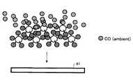
図3Aを参照するに、前記図1の被処理基板Wに対応する被処理基板41上には、Ru3(CO)12原料が、その分解を抑制する高濃度CO雰囲気と共に供給され、図3Bの工程において、前記被処理基板21の表面に吸着する。Referring to FIG. 3A, a Ru3 (CO)12 raw material is supplied along with a high-concentration CO atmosphere that suppresses decomposition on a
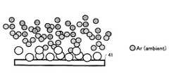
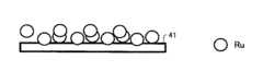
そこで図3Cの工程において前記雰囲気中にArガスなどの不活性ガスを供給して雰囲気中のCO濃度を低下させると、前記Ru3(CO)12化合物は直ちに分解し、その結果、前記被処理基板21上には前記図3Dに示すようにRuの原子層が残される。原料分子の分解の結果、CO配位子に起因するCOも発生するが、CO結合が切断されてCがRu原子層に混入するような状況は発生しない。すなわち、図3Dの工程では、非常に高純度のRu層を得ることができる。また、図3C,3Dの工程では、配位子起源のCOの割合はごくわずかであり、これが雰囲気中に放出されても、CO分圧が上昇して原料化合物の分解が妨げられる問題は生じない。すなわち、図3A〜3Dのプロセスでは、反応生成物が系から除外されるまで長時間パージ工程を行う必要ガない。Therefore, when an inert gas such as Ar gas is supplied to the atmosphere in the step of FIG. 3C to reduce the CO concentration in the atmosphere, the Ru3 (CO)12 compound is immediately decomposed, and as a result, the treatment target The Ru atomic layer is left on the
そこで、上記工程を繰り返すことにより、被処理基板表面に、任意の膜厚のRu膜を成膜することが可能となる。その際、本実施形態によるALD工程では、通常のALD工程に必要な原料ガスの吸着工程後の長時間にわたるパージ工程、さらに反応工程後の長時間にわたるパージ工程が不要で、図4のステップ1に示す原料導入および吸着工程とステップ2に示すCO分圧減少および分解工程とを繰り返すだけでよいため、成膜スループットを大きく増大させることができる。ただし図4は、前記図3A〜3Dの工程に対応するフローチャートであり、前記制御装置10Aは、図4のフローチャートに従って、図1の成膜装置10を制御する。 Therefore, by repeating the above steps, it is possible to form a Ru film having an arbitrary thickness on the surface of the substrate to be processed. In this case, the ALD process according to the present embodiment does not require a long-time purge process after the raw material gas adsorption process necessary for the normal ALD process and a long-time purge process after the reaction process, and therefore,
一例としては、前記図3A,3Bの工程においてRu3(CO)12ガスは1sccm程度の流量で、70〜100sccmの流量のCOガスと共に供給され、Arガスは供給されない。As an example, in the process of FIGS. 3A and 3B, Ru3 (CO)12 gas is supplied at a flow rate of about 1 sccm together with CO gas at a flow rate of 70 to 100 sccm, and no Ar gas is supplied.
一方、図3C,3Dの工程では、前記Ru3(CO)12ガスおよびCOガスの流量は変化させず、Arガスを例えば15sccmの流量で添加する。その際、処理容器12内部の全圧が変化しないように、例えば処理容器12に設けられた圧力計12Pにより前記処理容器12の内圧を測定し、その測定結果をもとに、前記制御装置10Aを使って前記コンダクタンスバルブ11aを制御してもよい。On the other hand, in the steps of FIGS. 3C and 3D, Ar gas is added at a flow rate of, for example, 15 sccm without changing the flow rates of the Ru3 (CO)12 gas and the CO gas. At that time, in order not to change the total pressure inside the
また、前記図3A〜3Dのプロセスにおいて、処理容器12の全圧を変化させて図3Bの状態から図3Cに成膜装置10の状態を遷移させてもよい。 3A to 3D, the state of the
なお、上記の説明はRu3(CO)12を原料とした場合についてのものであったが、本発明はかかる特定の原料に限定されるものではなく、例えばW(CO)6,Ni(CO)4,Mo(CO)6,Co2(CO)8,Rh4(CO)12,Re2(CO)10,Cr(CO)6などを原料として、それぞれの金属膜を形成する場合においても有効である。The above discussion is which was intended for the case where the raw materialRu 3(CO) 12, the present invention is not limited to such a specific material, for example,W (CO) 6, Ni ( CO )4 , Mo (CO)6 , Co2 (CO)8 , Rh4 (CO)12 , Re2 (CO)10 , Cr (CO)6, etc. as raw materials, even when forming each metal film It is valid.
また図3A〜3Dの工程において、下地層となる基板41は、シリコン基板であっても、シリコン酸化膜やその他の誘電体膜であっても、あるいは金属膜であってもよい。
[第2の実施形態]
図5A〜5Iは、本発明の第2の実施形態による多層配線構造の製造工程を示す。3A to 3D, the
[Second Embodiment]
5A to 5I show a manufacturing process of a multilayer wiring structure according to the second embodiment of the present invention.
図5Aを参照するに、シリコン基板21上に200nmの厚さに形成されたSiO2膜22中には幅が0.1μmで厚さが100nmのCuパターン22Aがダマシン法により、前記SiO2膜22の表面において露出するように形成されており、図5Bの工程で図5Aの構造上に、SiNバリア兼エッチングストッパ膜23と、SiCOH層間絶縁膜24と、SiNエッチングストッパ膜25と、SiCOH層間絶縁膜26と、SiNエッチングストッパ膜27とが、順次プラズマCVD法により形成される。Referring to FIG. 5A,
前記SiOCH膜24,26としては、市販のプラズマCVD法膜を使うことができるが、例えばかかるSiOCH膜24,26の形成を図示しない平行平板型高周波プラズマCVD装置で行う場合は、成膜を、約399Pa(3Torr)の圧力下、基板温度25℃で、Arガスを50SCCM、水素ガスを500SCCMの流量で供給し、周波数が13.50MHzの高周波を1000Wのパワーで供給することにより行うことができる。このようにして形成されたSiOCH膜24,26は約3.0の比誘電率を有する。またこのようなSiOCH膜の多孔質膜は、約2.2の比誘電率を有する。 As the
次に図5Cの工程において図示しないフォトリソグラフィ工程により前記SiN膜27を所望の配線パターンにパターニングし、さらに前記SiN膜27をハードマスクに前記層間絶縁膜26を前記SiN膜25が露出するまでドライエッチングし、前記層間絶縁膜26中に所望の配線パターンに対応した溝部26Aを形成する。さらに図5Cの工程では前記溝部26A中に露出した前記SiN膜25を所望のビアコンタクトにパターニングし、前記SiN膜25およびSiN膜27をハードマスクに前記層間絶縁膜24を前記SiN膜23が露出するまでドライエッチングし、前記層間絶縁膜24中に、前記ビアコンタクトに対応して、例えば径が16nm、あるいはそれ以下の開口部24Aを形成する。なお図5Cの工程で前記溝部26Aを形成する工程と開口部24Aを形成する工程の順序は逆転させてもよい。 Next, in the step of FIG. 5C, the
次に図5Dの工程において、前記開口部24Aの底部に露出したSiN膜23をエッチバックにより除去し、前記開口部24Aの底部に前記Cu配線パターンを露出させる。またこのSiN膜のエッチバック工程により、前記層間絶縁膜26上のSiN膜27が除去され、さらに前記配線溝26Aの底部のSiN膜25が除去される。 Next, in the step of FIG. 5D, the
次に図5Eの工程において図5Dの構造上にTaN膜とTa膜とを積層したバリアメタル膜28が、成膜ガスと還元ガスとを間にパージ工程を挟みながら繰り返し供給することで成膜を行う、いわゆるALD法により、2〜3nmの膜厚に形成される。 Next, in the process of FIG. 5E, a
次に図5Fの工程において、図5Eの構造は先に述べた図1の基板処理装置10の処理容器12に導入され、前記図3(A)〜(D)あるいは図4の工程を行うことにより、前記Ta膜28上にRu膜28Rが、2〜3nmの一様な膜厚で形成される。 Next, in the process of FIG. 5F, the structure of FIG. 5E is introduced into the
さらに図5Gの工程において、前記図5Fの構造上にCuシード層29がMOCVD法あるいはALD法により形成され、図5Hの工程において、前記図5Gの構造は電解めっき処理装置に移され、電解めっき法あるいは無電解めっき法により前記Cuシード層29上にCu層30が形成される。 Further, in the step of FIG. 5G, a
さらに熱処理の後、図5Iの工程において前記層間絶縁膜26上のCu層30およびその下のバリアメタル膜28がCMP(化学機械研磨)法により研磨除去され、前記配線溝26Aおよびビアホール24AをCuパターン30Aにより充填した配線構造が得られる。 Further, after the heat treatment, in the step of FIG. 5I, the
さらに上記図5A〜図5Iの工程を繰り返すことにより、図5Iの構造が繰り返された多層配線構造を形成することができる。 Further, by repeating the steps of FIGS. 5A to 5I, a multilayer wiring structure in which the structure of FIG. 5I is repeated can be formed.
本実施形態では、前記Ta膜18上にRu膜28Rが、先に述べた図3(A)〜(D)あるいは図4のALD工程により一様な膜厚で、形成されているため、その上に形成されるCuシード層29に凝集が発生することがなく、一様なシード層29が形成される。このため、かかるシード層29を使ったCu層30のメッキ法による成膜も、欠陥やボイドを形成することなく、一様に進行し、エレクトロマイグレーション耐性、あるいはストレスマイグレーション耐性に優れたCu配線パターンを得ることができる。 In this embodiment, the
以上、本発明を好ましい実施形態について説明したが、本発明はかかる特定の実施形態に限定されるものではなく、特許請求の範囲に記載した要旨内において様々な変形・変更が可能である。 As mentioned above, although this invention was described about preferable embodiment, this invention is not limited to this specific embodiment, A various deformation | transformation and change are possible within the summary described in the claim.
10 成膜装置
10A 制御装置
11 排気系
11A ターボ分子ポンプ
11B ドライポンプ
11C バイパスライン
11a 可変コンダクタンスバルブ
11b,11c,11d バルブ
12 処理容器
12G ゲートバルブ
12P 圧力計
13 基板保持台
13A ヒータ駆動ライン
14 原料供給系
14A ソースボトル
14B ガス導入ライン
14a バブリングガスライン
14d COガスライン
14b、14c,14e MFC
14f アルゴンガスラインDESCRIPTION OF
14f Argon gas line
Claims (11)
Translated fromJapanese前記被処理基板表面において前記気相成分の分圧を、前記カルボニル原料の分解が生じる第2の分圧に変化させ、前記被処理基板表面に前記金属元素を堆積させる第2の工程と、
よりなることを特徴とする金属膜の成膜方法。A metal element carbonyl raw material on the surface of the substrate to be processed is in the form of a gas phase molecule, together with a gas phase component that suppresses the decomposition of the gas phase molecule, and a partial pressure of the gas phase component, A first step of setting and supplying the first partial pressure to be suppressed;
A second step of changing the partial pressure of the vapor phase component on the surface of the substrate to be processed to a second partial pressure at which decomposition of the carbonyl raw material occurs, and depositing the metal element on the surface of the substrate to be processed;
A method for forming a metal film, comprising:
前記絶縁膜を、前記凹部を含め、バリアメタル膜により、前記凹部に整合した形状で覆う工程と、
前記バリアメタル膜上にRu膜を、前記凹部に整合した形状で形成する工程と、
前記Ru膜上にCuシード層を、前記凹部に整合した形状で形成する工程と、
前記Cuシード層を電極とした電解メッキを行うことにより、前記凹部をCu層により充填する工程と、
前記絶縁膜表面上のCu層を化学機械研磨により除去する工程と、
を含む多層配線構造の形成方法であって、
前記Ru膜を形成する工程は、
前記凹部を含む前記絶縁膜表面に、Ru3(CO)12原料を気相分子の形で、COガスと共に、前記COガス分圧を、Ru3(CO)12原料の分解が抑制される第1の分圧に設定して供給する第1の工程と、
前記COガスの分圧を、前記Ru3(CO)12原料の分解が生じる第2の分圧に変化させ、前記絶縁膜表面にRuを堆積させる第2の工程と、
よりなることを特徴とする多層配線構造の形成方法。Forming a recess in the insulating film;
Covering the insulating film with the barrier metal film including the concave portion in a shape aligned with the concave portion;
Forming a Ru film on the barrier metal film in a shape aligned with the recess;
Forming a Cu seed layer on the Ru film in a shape aligned with the recess;
Filling the recess with a Cu layer by performing electroplating using the Cu seed layer as an electrode;
Removing the Cu layer on the surface of the insulating film by chemical mechanical polishing;
A method for forming a multilayer wiring structure including:
The step of forming the Ru film includes:
On the surface of the insulating film including the concave portion, Ru3 (CO)12 raw material in the form of gas phase molecules, CO gas, the CO gas partial pressure, and decomposition of the Ru3 (CO)12 raw material are suppressed. A first step of setting and supplying one partial pressure;
Changing the partial pressure of the CO gas to a second partial pressure at which the Ru3 (CO)12 raw material is decomposed, and depositing Ru on the surface of the insulating film;
A method for forming a multilayer wiring structure, comprising:
前記多層配線構造を構成する層間絶縁膜中に凹部を形成する工程と、
前記層間絶縁膜を、前記凹部を含め、バリアメタル膜により、前記凹部に整合した形状で覆う工程と、
前記バリアメタル膜上にRu膜を、前記凹部に整合した形状で形成する工程と、
前記Ru膜上にCuシード層を、前記凹部に整合した形状で形成する工程と、
前記Cuシード層を電極とした電解メッキを行うことにより、前記凹部をCu層により充填する工程と、
前記層間絶縁膜表面上のCu層を化学機械研磨により除去する工程と、
を含み、
前記Ru膜を形成する工程は、
前記凹部を含む前記絶縁膜表面に、Ru3(CO)12原料を気相分子の形で、COガスと共に、前記COガス分圧を、Ru3(CO)12原料の分解が抑制される第1の分圧に設定して供給する第1の工程と、
前記COガスの分圧を、前記Ru3(CO)12原料の分解が生じる第2の分圧に変化させ、前記絶縁膜表面にRuを堆積させる第2の工程と、
よりなることを特徴とする半導体装置の製造方法。A method of manufacturing a semiconductor device having a multilayer wiring structure,
Forming a recess in an interlayer insulating film constituting the multilayer wiring structure;
Covering the interlayer insulating film with the barrier metal film including the recesses in a shape aligned with the recesses;
Forming a Ru film on the barrier metal film in a shape aligned with the recess;
Forming a Cu seed layer on the Ru film in a shape aligned with the recess;
Filling the recess with a Cu layer by performing electroplating using the Cu seed layer as an electrode;
Removing the Cu layer on the surface of the interlayer insulating film by chemical mechanical polishing;
Including
The step of forming the Ru film includes:
On the surface of the insulating film including the concave portion, Ru3 (CO)12 raw material in the form of gas phase molecules, CO gas, the CO gas partial pressure, and decomposition of the Ru3 (CO)12 raw material are suppressed. A first step of setting and supplying one partial pressure;
Changing the partial pressure of the CO gas to a second partial pressure at which the Ru3 (CO)12 raw material is decomposed, and depositing Ru on the surface of the insulating film;
A method for manufacturing a semiconductor device, comprising:
前記処理容器を排気する排気系と、
前記処理容器に金属カルボニル原料のガスを供給する第1のガス供給系と、
前記処理容器に、前記金属カルボニル原料の分解を抑制するガスを供給する第2のガス供給系と、
前記処理容器に、不活性ガスを供給する第3のガス供給系と、
前記第1,第2および第3のガス供給系を制御する制御部と、
を備えた成膜装置であって、
前記制御部は前記第3のガス供給系における前記不活性ガスの流量を制御し、前記処理容器中、前記被処理基板表面における前記金属カルボニル原料の分解を抑制するガスの分圧を、前記被処理基板表面において前記金属カルボニル原料の分解が抑制される第1の分圧と前記被処理基板表面において前記金属カルボニル原料の分解が生じる第2の分圧との間で変化させることを特徴とする成膜装置。A processing container having a substrate holding table for holding a substrate to be processed;
An exhaust system for exhausting the processing vessel;
A first gas supply system for supplying a metal carbonyl raw material gas to the processing vessel;
A second gas supply system for supplying a gas for suppressing decomposition of the metal carbonyl raw material to the processing container;
A third gas supply system for supplying an inert gas to the processing container;
A control unit for controlling the first, second and third gas supply systems;
A film forming apparatus comprising:
The control unit controls the flow rate of the inert gas in the third gas supply system, and the partial pressure of the gas that suppresses the decomposition of the metal carbonyl raw material on the surface of the substrate to be processed in the processing container is determined. It is changed between a first partial pressure at which decomposition of the metal carbonyl raw material is suppressed on the surface of the processing substrate and a second partial pressure at which decomposition of the metal carbonyl raw material occurs at the surface of the substrate to be processed. Deposition device.
Priority Applications (6)
| Application Number | Priority Date | Filing Date | Title |
|---|---|---|---|
| JP2007085021AJP2008244298A (en) | 2007-03-28 | 2007-03-28 | Film forming method of metal film, forming method of multilayer wiring structure, manufacturing method of semiconductor device, and film forming apparatus |
| PCT/JP2008/052459WO2008117582A1 (en) | 2007-03-28 | 2008-02-14 | Method for forming metal film using carbonyl material, method for forming multilayered wiring structure, method for manufacturing semiconductor device, and film forming apparatus |
| CN200880010346ACN101652836A (en) | 2007-03-28 | 2008-02-14 | Method for forming metal film using carbonyl material, method for forming multilayered wiring structure, method for manufacturing semiconductor device, and film forming apparatus |
| KR1020097020160AKR101188503B1 (en) | 2007-03-28 | 2008-02-14 | Method for forming metal film using carbonyl material, method for forming multilayered wiring structure, method for manufacturing semiconductor device, and film forming apparatus |
| TW097111062ATW200903644A (en) | 2007-03-28 | 2008-03-27 | Film forming method of metal film, forming method of multilayer wiring structure, manufacturing method of semiconductor device, and film forming apparatus |
| US12/568,082US20100015800A1 (en) | 2007-03-28 | 2009-09-28 | Method for forming metal film using carbonyl material, method for forming multi-layer wiring structure, and method for manufacturing semiconductor device |
Applications Claiming Priority (1)
| Application Number | Priority Date | Filing Date | Title |
|---|---|---|---|
| JP2007085021AJP2008244298A (en) | 2007-03-28 | 2007-03-28 | Film forming method of metal film, forming method of multilayer wiring structure, manufacturing method of semiconductor device, and film forming apparatus |
Publications (1)
| Publication Number | Publication Date |
|---|---|
| JP2008244298Atrue JP2008244298A (en) | 2008-10-09 |
Family
ID=39788321
Family Applications (1)
| Application Number | Title | Priority Date | Filing Date |
|---|---|---|---|
| JP2007085021APendingJP2008244298A (en) | 2007-03-28 | 2007-03-28 | Film forming method of metal film, forming method of multilayer wiring structure, manufacturing method of semiconductor device, and film forming apparatus |
Country Status (6)
| Country | Link |
|---|---|
| US (1) | US20100015800A1 (en) |
| JP (1) | JP2008244298A (en) |
| KR (1) | KR101188503B1 (en) |
| CN (1) | CN101652836A (en) |
| TW (1) | TW200903644A (en) |
| WO (1) | WO2008117582A1 (en) |
Cited By (7)
| Publication number | Priority date | Publication date | Assignee | Title |
|---|---|---|---|---|
| JP2010159447A (en)* | 2009-01-07 | 2010-07-22 | Jsr Corp | Method for depositing cobalt film |
| JP2012174844A (en)* | 2011-02-21 | 2012-09-10 | Tokyo Electron Ltd | Deposition method, deposition apparatus, semiconductor device and manufacturing method of the same |
| WO2015064353A1 (en)* | 2013-10-29 | 2015-05-07 | 田中貴金属工業株式会社 | Device for producing and method for producing dodecacarbonyl triruthenium |
| WO2015186679A1 (en)* | 2014-06-04 | 2015-12-10 | 田中貴金属工業株式会社 | Method for purifying dodecacarbonyl triruthenium |
| JP2016173392A (en)* | 2015-03-16 | 2016-09-29 | 株式会社東芝 | Light reflection type lithography mask, method of manufacturing the same, method of producing mask data, and mask blank |
| WO2022004520A1 (en)* | 2020-07-01 | 2022-01-06 | 東京エレクトロン株式会社 | Film forming method and film forming device |
| KR20230117590A (en) | 2020-12-15 | 2023-08-08 | 도쿄엘렉트론가부시키가이샤 | Substrate processing apparatus and substrate processing method |
Families Citing this family (12)
| Publication number | Priority date | Publication date | Assignee | Title |
|---|---|---|---|---|
| US7638074B2 (en) | 2006-03-10 | 2009-12-29 | Advanced Technology Materials, Inc. | Precursor compositions for atomic layer deposition and chemical vapor deposition of titanate, lanthanate, and tantalate dielectric films |
| JP2010177262A (en)* | 2009-01-27 | 2010-08-12 | Panasonic Corp | Method of manufacturing semiconductor device |
| KR101676060B1 (en)* | 2009-03-17 | 2016-11-14 | 엔테그리스, 아이엔씨. | Method and composition for depositing ruthenium with assistive metal species |
| JP2012117127A (en)* | 2010-12-02 | 2012-06-21 | Sumitomo Heavy Ind Ltd | Film deposition device, film deposition substrate manufacturing method, and film deposition substrate |
| CN102140625B (en)* | 2011-01-05 | 2013-07-17 | 景德镇陶瓷学院 | Method for preparing plasma-oriented tungsten coating used in fusion reactor by using tungsten carbonyl as precursor |
| WO2013177326A1 (en) | 2012-05-25 | 2013-11-28 | Advanced Technology Materials, Inc. | Silicon precursors for low temperature ald of silicon-based thin-films |
| US8736056B2 (en)* | 2012-07-31 | 2014-05-27 | Taiwan Semiconductor Manufacturing Company, Ltd. | Device for reducing contact resistance of a metal |
| JP5531120B1 (en)* | 2013-01-21 | 2014-06-25 | 田中貴金属工業株式会社 | Method for producing dodecacarbonyltriruthenium |
| WO2014124056A1 (en) | 2013-02-08 | 2014-08-14 | Advanced Technology Materials, Inc. | Ald processes for low leakage current and low equivalent oxide thickness bitao films |
| US10100407B2 (en)* | 2014-12-19 | 2018-10-16 | Lam Research Corporation | Hardware and process for film uniformity improvement |
| KR102551980B1 (en)* | 2016-03-30 | 2023-07-05 | 타호 리서치 리미티드 | Approaches to Strain Engineering of Perpendicular Magnetic Tunnel Junctions (PMTJS) and resulting structures |
| US9947621B2 (en) | 2016-08-05 | 2018-04-17 | International Business Machines Corporation | Structure and method to reduce copper loss during metal cap formation |
Citations (11)
| Publication number | Priority date | Publication date | Assignee | Title |
|---|---|---|---|---|
| JPH05259095A (en)* | 1992-03-12 | 1993-10-08 | Mitsubishi Materials Corp | Cvd method for gold film |
| JPH0778809A (en)* | 1993-09-07 | 1995-03-20 | Hitachi Ltd | Insulating film producing method and apparatus |
| JPH08139030A (en)* | 1994-11-09 | 1996-05-31 | Nippon Telegr & Teleph Corp <Ntt> | Method for forming copper thin film for wiring and method for manufacturing semiconductor device using the same |
| JP2001068468A (en)* | 1999-08-30 | 2001-03-16 | Tokyo Electron Ltd | Film formation method |
| JP2002231656A (en)* | 2001-01-31 | 2002-08-16 | Hitachi Ltd | Method for manufacturing semiconductor integrated circuit device |
| JP2003193233A (en)* | 2001-08-14 | 2003-07-09 | Tokyo Electron Ltd | Method for depositing tungsten film |
| JP2004273764A (en)* | 2003-03-07 | 2004-09-30 | Tokyo Electron Ltd | Method for forming tungsten film |
| JP2004346401A (en)* | 2003-05-23 | 2004-12-09 | Tokyo Electron Ltd | Film-forming method |
| JP2006005190A (en)* | 2004-06-18 | 2006-01-05 | Renesas Technology Corp | Semiconductor device |
| US20060110918A1 (en)* | 2004-11-23 | 2006-05-25 | Tokyo Electron Limited | Method and deposition system for increasing deposition rates of metal layers from metal-carbonyl precursors |
| JP2007501897A (en)* | 2003-08-08 | 2007-02-01 | ウェーバー・マニュファクチュリング・リミテッド | Hollow nickel molded product by vapor deposition |
Family Cites Families (4)
| Publication number | Priority date | Publication date | Assignee | Title |
|---|---|---|---|---|
| US7427426B2 (en)* | 2002-11-06 | 2008-09-23 | Tokyo Electron Limited | CVD method for forming metal film by using metal carbonyl gas |
| US6974768B1 (en)* | 2003-01-15 | 2005-12-13 | Novellus Systems, Inc. | Methods of providing an adhesion layer for adhesion of barrier and/or seed layers to dielectric films |
| US7300869B2 (en)* | 2004-09-20 | 2007-11-27 | Lsi Corporation | Integrated barrier and seed layer for copper interconnect technology |
| US7270848B2 (en)* | 2004-11-23 | 2007-09-18 | Tokyo Electron Limited | Method for increasing deposition rates of metal layers from metal-carbonyl precursors |
- 2007
- 2007-03-28JPJP2007085021Apatent/JP2008244298A/enactivePending
- 2008
- 2008-02-14KRKR1020097020160Apatent/KR101188503B1/enactiveActive
- 2008-02-14CNCN200880010346Apatent/CN101652836A/enactivePending
- 2008-02-14WOPCT/JP2008/052459patent/WO2008117582A1/enactiveApplication Filing
- 2008-03-27TWTW097111062Apatent/TW200903644A/enunknown
- 2009
- 2009-09-28USUS12/568,082patent/US20100015800A1/ennot_activeAbandoned
Patent Citations (11)
| Publication number | Priority date | Publication date | Assignee | Title |
|---|---|---|---|---|
| JPH05259095A (en)* | 1992-03-12 | 1993-10-08 | Mitsubishi Materials Corp | Cvd method for gold film |
| JPH0778809A (en)* | 1993-09-07 | 1995-03-20 | Hitachi Ltd | Insulating film producing method and apparatus |
| JPH08139030A (en)* | 1994-11-09 | 1996-05-31 | Nippon Telegr & Teleph Corp <Ntt> | Method for forming copper thin film for wiring and method for manufacturing semiconductor device using the same |
| JP2001068468A (en)* | 1999-08-30 | 2001-03-16 | Tokyo Electron Ltd | Film formation method |
| JP2002231656A (en)* | 2001-01-31 | 2002-08-16 | Hitachi Ltd | Method for manufacturing semiconductor integrated circuit device |
| JP2003193233A (en)* | 2001-08-14 | 2003-07-09 | Tokyo Electron Ltd | Method for depositing tungsten film |
| JP2004273764A (en)* | 2003-03-07 | 2004-09-30 | Tokyo Electron Ltd | Method for forming tungsten film |
| JP2004346401A (en)* | 2003-05-23 | 2004-12-09 | Tokyo Electron Ltd | Film-forming method |
| JP2007501897A (en)* | 2003-08-08 | 2007-02-01 | ウェーバー・マニュファクチュリング・リミテッド | Hollow nickel molded product by vapor deposition |
| JP2006005190A (en)* | 2004-06-18 | 2006-01-05 | Renesas Technology Corp | Semiconductor device |
| US20060110918A1 (en)* | 2004-11-23 | 2006-05-25 | Tokyo Electron Limited | Method and deposition system for increasing deposition rates of metal layers from metal-carbonyl precursors |
Cited By (16)
| Publication number | Priority date | Publication date | Assignee | Title |
|---|---|---|---|---|
| JP2010159447A (en)* | 2009-01-07 | 2010-07-22 | Jsr Corp | Method for depositing cobalt film |
| JP2012174844A (en)* | 2011-02-21 | 2012-09-10 | Tokyo Electron Ltd | Deposition method, deposition apparatus, semiconductor device and manufacturing method of the same |
| WO2015064353A1 (en)* | 2013-10-29 | 2015-05-07 | 田中貴金属工業株式会社 | Device for producing and method for producing dodecacarbonyl triruthenium |
| US9499411B2 (en) | 2013-10-29 | 2016-11-22 | Tanaka Kikinzoku Kogyo K.K. | Device for producing and method for producing dodecacarbonyl triruthenium |
| US9783429B2 (en) | 2014-06-04 | 2017-10-10 | Tanaka Kikinzoku Kogyo K.K. | Method for purifying dodecacarbonyl triruthenium |
| WO2015186679A1 (en)* | 2014-06-04 | 2015-12-10 | 田中貴金属工業株式会社 | Method for purifying dodecacarbonyl triruthenium |
| JP2015229639A (en)* | 2014-06-04 | 2015-12-21 | 田中貴金属工業株式会社 | Purification method of dodecacarbonyl triruthenium |
| US9946150B2 (en) | 2015-03-16 | 2018-04-17 | Toshiba Memory Corporation | Light reflection type lithography mask, its manufacturing method, mask data generation method and mask blank |
| JP2016173392A (en)* | 2015-03-16 | 2016-09-29 | 株式会社東芝 | Light reflection type lithography mask, method of manufacturing the same, method of producing mask data, and mask blank |
| WO2022004520A1 (en)* | 2020-07-01 | 2022-01-06 | 東京エレクトロン株式会社 | Film forming method and film forming device |
| JP2022012502A (en)* | 2020-07-01 | 2022-01-17 | 東京エレクトロン株式会社 | Film deposition method and film deposition apparatus |
| KR20230028471A (en) | 2020-07-01 | 2023-02-28 | 도쿄엘렉트론가부시키가이샤 | Film formation method and film formation apparatus |
| JP7507619B2 (en) | 2020-07-01 | 2024-06-28 | 東京エレクトロン株式会社 | Film forming method and film forming apparatus |
| US12344930B2 (en) | 2020-07-01 | 2025-07-01 | Tokyo Electron Limited | Deposition method and deposition apparatus |
| KR20230117590A (en) | 2020-12-15 | 2023-08-08 | 도쿄엘렉트론가부시키가이샤 | Substrate processing apparatus and substrate processing method |
| US12392033B2 (en) | 2020-12-15 | 2025-08-19 | Tokyo Electron Limited | Substrate processing apparatus and substrate processing method |
Also Published As
| Publication number | Publication date |
|---|---|
| US20100015800A1 (en) | 2010-01-21 |
| KR101188503B1 (en) | 2012-10-05 |
| TW200903644A (en) | 2009-01-16 |
| CN101652836A (en) | 2010-02-17 |
| WO2008117582A1 (en) | 2008-10-02 |
| KR20090126272A (en) | 2009-12-08 |
Similar Documents
| Publication | Publication Date | Title |
|---|---|---|
| KR101188503B1 (en) | Method for forming metal film using carbonyl material, method for forming multilayered wiring structure, method for manufacturing semiconductor device, and film forming apparatus | |
| US11587829B2 (en) | Doping control of metal nitride films | |
| KR102189781B1 (en) | Methods for depositing manganese and manganese nitrides | |
| US9076661B2 (en) | Methods for manganese nitride integration | |
| US12211743B2 (en) | Method of forming a metal liner for interconnect structures | |
| JP2005347472A (en) | Substrate processing method and manufacturing method of semiconductor device | |
| KR101882991B1 (en) | Ruthenium film forming method, film forming apparatus, and semiconductor device manufacturing method | |
| CN109461698B (en) | Seed layer for copper interconnect | |
| KR101730229B1 (en) | Ruthenium film forming method, ruthenium film forming apparatus, and semiconductor device manufacturing method | |
| JP2003243497A (en) | Wiring structure and method of forming the same | |
| TWI609095B (en) | Methods for manganese nitride integration | |
| US20230253248A1 (en) | Methods of forming metal liner for interconnect structures | |
| KR100922905B1 (en) | Film forming method, semiconductor device manufacturing method, semiconductor device, program and recording medium | |
| US20240258164A1 (en) | Methods of forming interconnect structures |
Legal Events
| Date | Code | Title | Description |
|---|---|---|---|
| A621 | Written request for application examination | Free format text:JAPANESE INTERMEDIATE CODE: A621 Effective date:20100113 | |
| A131 | Notification of reasons for refusal | Free format text:JAPANESE INTERMEDIATE CODE: A131 Effective date:20121211 | |
| A521 | Written amendment | Free format text:JAPANESE INTERMEDIATE CODE: A523 Effective date:20130208 | |
| A02 | Decision of refusal | Free format text:JAPANESE INTERMEDIATE CODE: A02 Effective date:20130319 |