JP2008244191A - Manufacturing method of component-embedded substrate - Google Patents
Manufacturing method of component-embedded substrateDownload PDFInfo
- Publication number
- JP2008244191A JP2008244191AJP2007083397AJP2007083397AJP2008244191AJP 2008244191 AJP2008244191 AJP 2008244191AJP 2007083397 AJP2007083397 AJP 2007083397AJP 2007083397 AJP2007083397 AJP 2007083397AJP 2008244191 AJP2008244191 AJP 2008244191A
- Authority
- JP
- Japan
- Prior art keywords
- component
- connection
- metal particles
- manufacturing
- circuit board
- Prior art date
- Legal status (The legal status is an assumption and is not a legal conclusion. Google has not performed a legal analysis and makes no representation as to the accuracy of the status listed.)
- Pending
Links
Images


Classifications
- H—ELECTRICITY
- H01—ELECTRIC ELEMENTS
- H01L—SEMICONDUCTOR DEVICES NOT COVERED BY CLASS H10
- H01L24/00—Arrangements for connecting or disconnecting semiconductor or solid-state bodies; Methods or apparatus related thereto
- H01L24/01—Means for bonding being attached to, or being formed on, the surface to be connected, e.g. chip-to-package, die-attach, "first-level" interconnects; Manufacturing methods related thereto
- H01L24/26—Layer connectors, e.g. plate connectors, solder or adhesive layers; Manufacturing methods related thereto
- H01L24/28—Structure, shape, material or disposition of the layer connectors prior to the connecting process
- H01L24/29—Structure, shape, material or disposition of the layer connectors prior to the connecting process of an individual layer connector
- H—ELECTRICITY
- H01—ELECTRIC ELEMENTS
- H01L—SEMICONDUCTOR DEVICES NOT COVERED BY CLASS H10
- H01L21/00—Processes or apparatus adapted for the manufacture or treatment of semiconductor or solid state devices or of parts thereof
- H01L21/02—Manufacture or treatment of semiconductor devices or of parts thereof
- H01L21/04—Manufacture or treatment of semiconductor devices or of parts thereof the devices having potential barriers, e.g. a PN junction, depletion layer or carrier concentration layer
- H01L21/48—Manufacture or treatment of parts, e.g. containers, prior to assembly of the devices, using processes not provided for in a single one of the groups H01L21/18 - H01L21/326 or H10D48/04 - H10D48/07
- H01L21/4814—Conductive parts
- H01L21/4846—Leads on or in insulating or insulated substrates, e.g. metallisation
- H01L21/4857—Multilayer substrates
- H—ELECTRICITY
- H01—ELECTRIC ELEMENTS
- H01L—SEMICONDUCTOR DEVICES NOT COVERED BY CLASS H10
- H01L23/00—Details of semiconductor or other solid state devices
- H01L23/52—Arrangements for conducting electric current within the device in operation from one component to another, i.e. interconnections, e.g. wires, lead frames
- H01L23/538—Arrangements for conducting electric current within the device in operation from one component to another, i.e. interconnections, e.g. wires, lead frames the interconnection structure between a plurality of semiconductor chips being formed on, or in, insulating substrates
- H01L23/5389—Arrangements for conducting electric current within the device in operation from one component to another, i.e. interconnections, e.g. wires, lead frames the interconnection structure between a plurality of semiconductor chips being formed on, or in, insulating substrates the chips being integrally enclosed by the interconnect and support structures
- H—ELECTRICITY
- H01—ELECTRIC ELEMENTS
- H01L—SEMICONDUCTOR DEVICES NOT COVERED BY CLASS H10
- H01L24/00—Arrangements for connecting or disconnecting semiconductor or solid-state bodies; Methods or apparatus related thereto
- H01L24/80—Methods for connecting semiconductor or other solid state bodies using means for bonding being attached to, or being formed on, the surface to be connected
- H01L24/83—Methods for connecting semiconductor or other solid state bodies using means for bonding being attached to, or being formed on, the surface to be connected using a layer connector
- H—ELECTRICITY
- H01—ELECTRIC ELEMENTS
- H01L—SEMICONDUCTOR DEVICES NOT COVERED BY CLASS H10
- H01L24/00—Arrangements for connecting or disconnecting semiconductor or solid-state bodies; Methods or apparatus related thereto
- H01L24/90—Methods for connecting semiconductor or solid state bodies using means for bonding not being attached to, or not being formed on, the body surface to be connected, e.g. pressure contacts using springs or clips
- H—ELECTRICITY
- H01—ELECTRIC ELEMENTS
- H01L—SEMICONDUCTOR DEVICES NOT COVERED BY CLASS H10
- H01L2224/00—Indexing scheme for arrangements for connecting or disconnecting semiconductor or solid-state bodies and methods related thereto as covered by H01L24/00
- H01L2224/01—Means for bonding being attached to, or being formed on, the surface to be connected, e.g. chip-to-package, die-attach, "first-level" interconnects; Manufacturing methods related thereto
- H01L2224/10—Bump connectors; Manufacturing methods related thereto
- H01L2224/11—Manufacturing methods
- H01L2224/113—Manufacturing methods by local deposition of the material of the bump connector
- H01L2224/1133—Manufacturing methods by local deposition of the material of the bump connector in solid form
- H01L2224/11332—Manufacturing methods by local deposition of the material of the bump connector in solid form using a powder
- H—ELECTRICITY
- H01—ELECTRIC ELEMENTS
- H01L—SEMICONDUCTOR DEVICES NOT COVERED BY CLASS H10
- H01L2224/00—Indexing scheme for arrangements for connecting or disconnecting semiconductor or solid-state bodies and methods related thereto as covered by H01L24/00
- H01L2224/01—Means for bonding being attached to, or being formed on, the surface to be connected, e.g. chip-to-package, die-attach, "first-level" interconnects; Manufacturing methods related thereto
- H01L2224/10—Bump connectors; Manufacturing methods related thereto
- H01L2224/11—Manufacturing methods
- H01L2224/118—Post-treatment of the bump connector
- H01L2224/1182—Applying permanent coating, e.g. in-situ coating
- H01L2224/11822—Applying permanent coating, e.g. in-situ coating by dipping, e.g. in a solder bath
- H—ELECTRICITY
- H01—ELECTRIC ELEMENTS
- H01L—SEMICONDUCTOR DEVICES NOT COVERED BY CLASS H10
- H01L2224/00—Indexing scheme for arrangements for connecting or disconnecting semiconductor or solid-state bodies and methods related thereto as covered by H01L24/00
- H01L2224/01—Means for bonding being attached to, or being formed on, the surface to be connected, e.g. chip-to-package, die-attach, "first-level" interconnects; Manufacturing methods related thereto
- H01L2224/10—Bump connectors; Manufacturing methods related thereto
- H01L2224/12—Structure, shape, material or disposition of the bump connectors prior to the connecting process
- H01L2224/13—Structure, shape, material or disposition of the bump connectors prior to the connecting process of an individual bump connector
- H01L2224/13001—Core members of the bump connector
- H01L2224/13099—Material
- H01L2224/131—Material with a principal constituent of the material being a metal or a metalloid, e.g. boron [B], silicon [Si], germanium [Ge], arsenic [As], antimony [Sb], tellurium [Te] and polonium [Po], and alloys thereof
- H01L2224/13138—Material with a principal constituent of the material being a metal or a metalloid, e.g. boron [B], silicon [Si], germanium [Ge], arsenic [As], antimony [Sb], tellurium [Te] and polonium [Po], and alloys thereof the principal constituent melting at a temperature of greater than or equal to 950°C and less than 1550°C
- H01L2224/13144—Gold [Au] as principal constituent
- H—ELECTRICITY
- H01—ELECTRIC ELEMENTS
- H01L—SEMICONDUCTOR DEVICES NOT COVERED BY CLASS H10
- H01L2224/00—Indexing scheme for arrangements for connecting or disconnecting semiconductor or solid-state bodies and methods related thereto as covered by H01L24/00
- H01L2224/01—Means for bonding being attached to, or being formed on, the surface to be connected, e.g. chip-to-package, die-attach, "first-level" interconnects; Manufacturing methods related thereto
- H01L2224/10—Bump connectors; Manufacturing methods related thereto
- H01L2224/15—Structure, shape, material or disposition of the bump connectors after the connecting process
- H01L2224/16—Structure, shape, material or disposition of the bump connectors after the connecting process of an individual bump connector
- H01L2224/161—Disposition
- H01L2224/16151—Disposition the bump connector connecting between a semiconductor or solid-state body and an item not being a semiconductor or solid-state body, e.g. chip-to-substrate, chip-to-passive
- H01L2224/16221—Disposition the bump connector connecting between a semiconductor or solid-state body and an item not being a semiconductor or solid-state body, e.g. chip-to-substrate, chip-to-passive the body and the item being stacked
- H01L2224/16225—Disposition the bump connector connecting between a semiconductor or solid-state body and an item not being a semiconductor or solid-state body, e.g. chip-to-substrate, chip-to-passive the body and the item being stacked the item being non-metallic, e.g. insulating substrate with or without metallisation
- H01L2224/16235—Disposition the bump connector connecting between a semiconductor or solid-state body and an item not being a semiconductor or solid-state body, e.g. chip-to-substrate, chip-to-passive the body and the item being stacked the item being non-metallic, e.g. insulating substrate with or without metallisation the bump connector connecting to a via metallisation of the item
- H—ELECTRICITY
- H01—ELECTRIC ELEMENTS
- H01L—SEMICONDUCTOR DEVICES NOT COVERED BY CLASS H10
- H01L2224/00—Indexing scheme for arrangements for connecting or disconnecting semiconductor or solid-state bodies and methods related thereto as covered by H01L24/00
- H01L2224/01—Means for bonding being attached to, or being formed on, the surface to be connected, e.g. chip-to-package, die-attach, "first-level" interconnects; Manufacturing methods related thereto
- H01L2224/18—High density interconnect [HDI] connectors; Manufacturing methods related thereto
- H01L2224/23—Structure, shape, material or disposition of the high density interconnect connectors after the connecting process
- H01L2224/24—Structure, shape, material or disposition of the high density interconnect connectors after the connecting process of an individual high density interconnect connector
- H01L2224/2401—Structure
- H01L2224/2402—Laminated, e.g. MCM-L type
- H—ELECTRICITY
- H01—ELECTRIC ELEMENTS
- H01L—SEMICONDUCTOR DEVICES NOT COVERED BY CLASS H10
- H01L2224/00—Indexing scheme for arrangements for connecting or disconnecting semiconductor or solid-state bodies and methods related thereto as covered by H01L24/00
- H01L2224/01—Means for bonding being attached to, or being formed on, the surface to be connected, e.g. chip-to-package, die-attach, "first-level" interconnects; Manufacturing methods related thereto
- H01L2224/18—High density interconnect [HDI] connectors; Manufacturing methods related thereto
- H01L2224/23—Structure, shape, material or disposition of the high density interconnect connectors after the connecting process
- H01L2224/24—Structure, shape, material or disposition of the high density interconnect connectors after the connecting process of an individual high density interconnect connector
- H01L2224/241—Disposition
- H01L2224/24151—Connecting between a semiconductor or solid-state body and an item not being a semiconductor or solid-state body, e.g. chip-to-substrate, chip-to-passive
- H01L2224/24221—Connecting between a semiconductor or solid-state body and an item not being a semiconductor or solid-state body, e.g. chip-to-substrate, chip-to-passive the body and the item being stacked
- H01L2224/24225—Connecting between a semiconductor or solid-state body and an item not being a semiconductor or solid-state body, e.g. chip-to-substrate, chip-to-passive the body and the item being stacked the item being non-metallic, e.g. insulating substrate with or without metallisation
- H01L2224/24226—Connecting between a semiconductor or solid-state body and an item not being a semiconductor or solid-state body, e.g. chip-to-substrate, chip-to-passive the body and the item being stacked the item being non-metallic, e.g. insulating substrate with or without metallisation the HDI interconnect connecting to the same level of the item at which the semiconductor or solid-state body is mounted, e.g. the item being planar
- H—ELECTRICITY
- H01—ELECTRIC ELEMENTS
- H01L—SEMICONDUCTOR DEVICES NOT COVERED BY CLASS H10
- H01L2224/00—Indexing scheme for arrangements for connecting or disconnecting semiconductor or solid-state bodies and methods related thereto as covered by H01L24/00
- H01L2224/01—Means for bonding being attached to, or being formed on, the surface to be connected, e.g. chip-to-package, die-attach, "first-level" interconnects; Manufacturing methods related thereto
- H01L2224/26—Layer connectors, e.g. plate connectors, solder or adhesive layers; Manufacturing methods related thereto
- H01L2224/28—Structure, shape, material or disposition of the layer connectors prior to the connecting process
- H01L2224/29—Structure, shape, material or disposition of the layer connectors prior to the connecting process of an individual layer connector
- H01L2224/29001—Core members of the layer connector
- H01L2224/29099—Material
- H01L2224/291—Material with a principal constituent of the material being a metal or a metalloid, e.g. boron [B], silicon [Si], germanium [Ge], arsenic [As], antimony [Sb], tellurium [Te] and polonium [Po], and alloys thereof
- H01L2224/29101—Material with a principal constituent of the material being a metal or a metalloid, e.g. boron [B], silicon [Si], germanium [Ge], arsenic [As], antimony [Sb], tellurium [Te] and polonium [Po], and alloys thereof the principal constituent melting at a temperature of less than 400°C
- H—ELECTRICITY
- H01—ELECTRIC ELEMENTS
- H01L—SEMICONDUCTOR DEVICES NOT COVERED BY CLASS H10
- H01L2224/00—Indexing scheme for arrangements for connecting or disconnecting semiconductor or solid-state bodies and methods related thereto as covered by H01L24/00
- H01L2224/01—Means for bonding being attached to, or being formed on, the surface to be connected, e.g. chip-to-package, die-attach, "first-level" interconnects; Manufacturing methods related thereto
- H01L2224/26—Layer connectors, e.g. plate connectors, solder or adhesive layers; Manufacturing methods related thereto
- H01L2224/28—Structure, shape, material or disposition of the layer connectors prior to the connecting process
- H01L2224/29—Structure, shape, material or disposition of the layer connectors prior to the connecting process of an individual layer connector
- H01L2224/29001—Core members of the layer connector
- H01L2224/29099—Material
- H01L2224/2919—Material with a principal constituent of the material being a polymer, e.g. polyester, phenolic based polymer, epoxy
- H—ELECTRICITY
- H01—ELECTRIC ELEMENTS
- H01L—SEMICONDUCTOR DEVICES NOT COVERED BY CLASS H10
- H01L2224/00—Indexing scheme for arrangements for connecting or disconnecting semiconductor or solid-state bodies and methods related thereto as covered by H01L24/00
- H01L2224/01—Means for bonding being attached to, or being formed on, the surface to be connected, e.g. chip-to-package, die-attach, "first-level" interconnects; Manufacturing methods related thereto
- H01L2224/26—Layer connectors, e.g. plate connectors, solder or adhesive layers; Manufacturing methods related thereto
- H01L2224/28—Structure, shape, material or disposition of the layer connectors prior to the connecting process
- H01L2224/29—Structure, shape, material or disposition of the layer connectors prior to the connecting process of an individual layer connector
- H01L2224/29001—Core members of the layer connector
- H01L2224/29099—Material
- H01L2224/29198—Material with a principal constituent of the material being a combination of two or more materials in the form of a matrix with a filler, i.e. being a hybrid material, e.g. segmented structures, foams
- H01L2224/29298—Fillers
- H01L2224/29299—Base material
- H01L2224/293—Base material with a principal constituent of the material being a metal or a metalloid, e.g. boron [B], silicon [Si], germanium [Ge], arsenic [As], antimony [Sb], tellurium [Te] and polonium [Po], and alloys thereof
- H01L2224/29338—Base material with a principal constituent of the material being a metal or a metalloid, e.g. boron [B], silicon [Si], germanium [Ge], arsenic [As], antimony [Sb], tellurium [Te] and polonium [Po], and alloys thereof the principal constituent melting at a temperature of greater than or equal to 950°C and less than 1550°C
- H01L2224/29339—Silver [Ag] as principal constituent
- H—ELECTRICITY
- H01—ELECTRIC ELEMENTS
- H01L—SEMICONDUCTOR DEVICES NOT COVERED BY CLASS H10
- H01L2224/00—Indexing scheme for arrangements for connecting or disconnecting semiconductor or solid-state bodies and methods related thereto as covered by H01L24/00
- H01L2224/01—Means for bonding being attached to, or being formed on, the surface to be connected, e.g. chip-to-package, die-attach, "first-level" interconnects; Manufacturing methods related thereto
- H01L2224/26—Layer connectors, e.g. plate connectors, solder or adhesive layers; Manufacturing methods related thereto
- H01L2224/31—Structure, shape, material or disposition of the layer connectors after the connecting process
- H01L2224/32—Structure, shape, material or disposition of the layer connectors after the connecting process of an individual layer connector
- H01L2224/321—Disposition
- H01L2224/32151—Disposition the layer connector connecting between a semiconductor or solid-state body and an item not being a semiconductor or solid-state body, e.g. chip-to-substrate, chip-to-passive
- H01L2224/32221—Disposition the layer connector connecting between a semiconductor or solid-state body and an item not being a semiconductor or solid-state body, e.g. chip-to-substrate, chip-to-passive the body and the item being stacked
- H01L2224/32225—Disposition the layer connector connecting between a semiconductor or solid-state body and an item not being a semiconductor or solid-state body, e.g. chip-to-substrate, chip-to-passive the body and the item being stacked the item being non-metallic, e.g. insulating substrate with or without metallisation
- H—ELECTRICITY
- H01—ELECTRIC ELEMENTS
- H01L—SEMICONDUCTOR DEVICES NOT COVERED BY CLASS H10
- H01L2224/00—Indexing scheme for arrangements for connecting or disconnecting semiconductor or solid-state bodies and methods related thereto as covered by H01L24/00
- H01L2224/73—Means for bonding being of different types provided for in two or more of groups H01L2224/10, H01L2224/18, H01L2224/26, H01L2224/34, H01L2224/42, H01L2224/50, H01L2224/63, H01L2224/71
- H01L2224/732—Location after the connecting process
- H01L2224/73201—Location after the connecting process on the same surface
- H01L2224/73203—Bump and layer connectors
- H01L2224/73204—Bump and layer connectors the bump connector being embedded into the layer connector
- H—ELECTRICITY
- H01—ELECTRIC ELEMENTS
- H01L—SEMICONDUCTOR DEVICES NOT COVERED BY CLASS H10
- H01L2224/00—Indexing scheme for arrangements for connecting or disconnecting semiconductor or solid-state bodies and methods related thereto as covered by H01L24/00
- H01L2224/80—Methods for connecting semiconductor or other solid state bodies using means for bonding being attached to, or being formed on, the surface to be connected
- H01L2224/81—Methods for connecting semiconductor or other solid state bodies using means for bonding being attached to, or being formed on, the surface to be connected using a bump connector
- H01L2224/818—Bonding techniques
- H01L2224/8184—Sintering
- H—ELECTRICITY
- H01—ELECTRIC ELEMENTS
- H01L—SEMICONDUCTOR DEVICES NOT COVERED BY CLASS H10
- H01L2224/00—Indexing scheme for arrangements for connecting or disconnecting semiconductor or solid-state bodies and methods related thereto as covered by H01L24/00
- H01L2224/80—Methods for connecting semiconductor or other solid state bodies using means for bonding being attached to, or being formed on, the surface to be connected
- H01L2224/83—Methods for connecting semiconductor or other solid state bodies using means for bonding being attached to, or being formed on, the surface to be connected using a layer connector
- H01L2224/8319—Arrangement of the layer connectors prior to mounting
- H01L2224/83191—Arrangement of the layer connectors prior to mounting wherein the layer connectors are disposed only on the semiconductor or solid-state body
- H—ELECTRICITY
- H01—ELECTRIC ELEMENTS
- H01L—SEMICONDUCTOR DEVICES NOT COVERED BY CLASS H10
- H01L2224/00—Indexing scheme for arrangements for connecting or disconnecting semiconductor or solid-state bodies and methods related thereto as covered by H01L24/00
- H01L2224/80—Methods for connecting semiconductor or other solid state bodies using means for bonding being attached to, or being formed on, the surface to be connected
- H01L2224/83—Methods for connecting semiconductor or other solid state bodies using means for bonding being attached to, or being formed on, the surface to be connected using a layer connector
- H01L2224/8319—Arrangement of the layer connectors prior to mounting
- H01L2224/83192—Arrangement of the layer connectors prior to mounting wherein the layer connectors are disposed only on another item or body to be connected to the semiconductor or solid-state body
- H—ELECTRICITY
- H01—ELECTRIC ELEMENTS
- H01L—SEMICONDUCTOR DEVICES NOT COVERED BY CLASS H10
- H01L2224/00—Indexing scheme for arrangements for connecting or disconnecting semiconductor or solid-state bodies and methods related thereto as covered by H01L24/00
- H01L2224/80—Methods for connecting semiconductor or other solid state bodies using means for bonding being attached to, or being formed on, the surface to be connected
- H01L2224/83—Methods for connecting semiconductor or other solid state bodies using means for bonding being attached to, or being formed on, the surface to be connected using a layer connector
- H01L2224/838—Bonding techniques
- H01L2224/8385—Bonding techniques using a polymer adhesive, e.g. an adhesive based on silicone, epoxy, polyimide, polyester
- H01L2224/83855—Hardening the adhesive by curing, i.e. thermosetting
- H—ELECTRICITY
- H01—ELECTRIC ELEMENTS
- H01L—SEMICONDUCTOR DEVICES NOT COVERED BY CLASS H10
- H01L2924/00—Indexing scheme for arrangements or methods for connecting or disconnecting semiconductor or solid-state bodies as covered by H01L24/00
- H01L2924/01—Chemical elements
- H01L2924/01006—Carbon [C]
- H—ELECTRICITY
- H01—ELECTRIC ELEMENTS
- H01L—SEMICONDUCTOR DEVICES NOT COVERED BY CLASS H10
- H01L2924/00—Indexing scheme for arrangements or methods for connecting or disconnecting semiconductor or solid-state bodies as covered by H01L24/00
- H01L2924/01—Chemical elements
- H01L2924/01029—Copper [Cu]
- H—ELECTRICITY
- H01—ELECTRIC ELEMENTS
- H01L—SEMICONDUCTOR DEVICES NOT COVERED BY CLASS H10
- H01L2924/00—Indexing scheme for arrangements or methods for connecting or disconnecting semiconductor or solid-state bodies as covered by H01L24/00
- H01L2924/01—Chemical elements
- H01L2924/0103—Zinc [Zn]
- H—ELECTRICITY
- H01—ELECTRIC ELEMENTS
- H01L—SEMICONDUCTOR DEVICES NOT COVERED BY CLASS H10
- H01L2924/00—Indexing scheme for arrangements or methods for connecting or disconnecting semiconductor or solid-state bodies as covered by H01L24/00
- H01L2924/01—Chemical elements
- H01L2924/01033—Arsenic [As]
- H—ELECTRICITY
- H01—ELECTRIC ELEMENTS
- H01L—SEMICONDUCTOR DEVICES NOT COVERED BY CLASS H10
- H01L2924/00—Indexing scheme for arrangements or methods for connecting or disconnecting semiconductor or solid-state bodies as covered by H01L24/00
- H01L2924/01—Chemical elements
- H01L2924/01047—Silver [Ag]
- H—ELECTRICITY
- H01—ELECTRIC ELEMENTS
- H01L—SEMICONDUCTOR DEVICES NOT COVERED BY CLASS H10
- H01L2924/00—Indexing scheme for arrangements or methods for connecting or disconnecting semiconductor or solid-state bodies as covered by H01L24/00
- H01L2924/01—Chemical elements
- H01L2924/0105—Tin [Sn]
- H—ELECTRICITY
- H01—ELECTRIC ELEMENTS
- H01L—SEMICONDUCTOR DEVICES NOT COVERED BY CLASS H10
- H01L2924/00—Indexing scheme for arrangements or methods for connecting or disconnecting semiconductor or solid-state bodies as covered by H01L24/00
- H01L2924/01—Chemical elements
- H01L2924/01078—Platinum [Pt]
- H—ELECTRICITY
- H01—ELECTRIC ELEMENTS
- H01L—SEMICONDUCTOR DEVICES NOT COVERED BY CLASS H10
- H01L2924/00—Indexing scheme for arrangements or methods for connecting or disconnecting semiconductor or solid-state bodies as covered by H01L24/00
- H01L2924/01—Chemical elements
- H01L2924/01079—Gold [Au]
- H—ELECTRICITY
- H01—ELECTRIC ELEMENTS
- H01L—SEMICONDUCTOR DEVICES NOT COVERED BY CLASS H10
- H01L2924/00—Indexing scheme for arrangements or methods for connecting or disconnecting semiconductor or solid-state bodies as covered by H01L24/00
- H01L2924/013—Alloys
- H01L2924/014—Solder alloys
- H—ELECTRICITY
- H01—ELECTRIC ELEMENTS
- H01L—SEMICONDUCTOR DEVICES NOT COVERED BY CLASS H10
- H01L2924/00—Indexing scheme for arrangements or methods for connecting or disconnecting semiconductor or solid-state bodies as covered by H01L24/00
- H01L2924/06—Polymers
- H01L2924/0665—Epoxy resin
- H—ELECTRICITY
- H01—ELECTRIC ELEMENTS
- H01L—SEMICONDUCTOR DEVICES NOT COVERED BY CLASS H10
- H01L2924/00—Indexing scheme for arrangements or methods for connecting or disconnecting semiconductor or solid-state bodies as covered by H01L24/00
- H01L2924/06—Polymers
- H01L2924/078—Adhesive characteristics other than chemical
- H01L2924/0781—Adhesive characteristics other than chemical being an ohmic electrical conductor
- H—ELECTRICITY
- H01—ELECTRIC ELEMENTS
- H01L—SEMICONDUCTOR DEVICES NOT COVERED BY CLASS H10
- H01L2924/00—Indexing scheme for arrangements or methods for connecting or disconnecting semiconductor or solid-state bodies as covered by H01L24/00
- H01L2924/10—Details of semiconductor or other solid state devices to be connected
- H01L2924/11—Device type
- H01L2924/14—Integrated circuits
Landscapes
- Engineering & Computer Science (AREA)
- Computer Hardware Design (AREA)
- Microelectronics & Electronic Packaging (AREA)
- Power Engineering (AREA)
- Physics & Mathematics (AREA)
- Condensed Matter Physics & Semiconductors (AREA)
- General Physics & Mathematics (AREA)
- Ceramic Engineering (AREA)
- Manufacturing & Machinery (AREA)
- Production Of Multi-Layered Print Wiring Board (AREA)
Abstract
Translated fromJapaneseDescription
Translated fromJapanese本発明は部品内蔵基板の製造方法に関するものであり、電子部品、特に、半導体素子を内蔵した部品内蔵基板における電子部品の実装密度を高めるための構成に特徴のある部品内蔵基板の製造方法に関するものである。 The present invention relates to a method of manufacturing a component-embedded substrate, and more particularly to a method of manufacturing a component-embedded substrate characterized by a configuration for increasing the mounting density of electronic components in a component-embedded substrate incorporating a semiconductor element. It is.
近年の携帯情報機器等の小型化・高性能化に伴って、携帯情報機器等に搭載する半導体装置モジュール等の小型化・高密度実装化が求められており、それに伴って半導体素子等の電子部品自体も小型化され、電子部品に設けるバンプ電極等の間隔が狭くなっている。 With recent downsizing and higher performance of portable information devices, etc., there has been a demand for downsizing and high-density mounting of semiconductor device modules and the like mounted on portable information devices. The components themselves are also miniaturized, and the intervals between bump electrodes and the like provided on the electronic components are narrowed.
このような高密度実装の要請に応えるために、半導体チップや受動部品を多層回路基板の表面に実装していた従来の表面実装に代えて、半導体チップ等を多層回路基板の中に埋め込む部品内蔵基板が開発されている(例えば、特許文献1参照)。 In order to meet the demand for such high-density mounting, instead of the conventional surface mounting in which semiconductor chips and passive components are mounted on the surface of the multilayer circuit board, a built-in component in which the semiconductor chip is embedded in the multilayer circuit board A substrate has been developed (see, for example, Patent Document 1).
この部品内蔵基板においては、表面実装に比べて電子部品を配置する自由度が高くなるとともに、電子部品間の配線の最適化により高周波特性を改善することができる等の利点がある。 This component-embedded substrate has advantages that the degree of freedom for arranging electronic components is higher than that of surface mounting, and that high-frequency characteristics can be improved by optimizing the wiring between the electronic components.
現在は、このような部品内蔵基板は、高密度実装の要請の大きな携帯電話機器に、携帯電話に求められる各種の機能の内の一部の機能を切り出したモジュールとして使用されているが、内蔵する電子部品の種類を増やすことによって、メインボード等への適用も可能になる。 Currently, such component-embedded boards are used as modules that cut out some of the various functions required for mobile phones in mobile phone devices that require high-density mounting. By increasing the types of electronic components to be used, application to a main board or the like becomes possible.
また、この部品内蔵基板においては、多層回路基板上に電子部品を実装する場合には、フリップチップ方式が採用されており、このフリップチップ方式の接合の一つとして、接着剤を硬化させると同時に高荷重を印加してAuスタッドバンプを押し潰すことにより多層回路基板の内層回路電極とをコンタクトさせる圧接方式がある(例えば、特許文献2参照)。 In addition, in this component built-in substrate, when mounting electronic components on a multilayer circuit board, a flip chip method is adopted, and as one of the flip chip method joints, the adhesive is cured at the same time. There is a pressure contact method in which an Au stud bump is crushed by applying a high load to contact an inner layer circuit electrode of a multilayer circuit board (see, for example, Patent Document 2).
この接合方式は、接着剤を硬化させるときの収縮力と、Auスタッドバンプと多層回路基板の内層回路電極を押しつぶしたときの反発力を利用して、接触を維持させることにより電気的接続を維持するものである。
近年の半導体素子の高性能化に伴い、Auスタッドバンプが挟ピッチ化されており、これに伴いAuスタッドバンプのサイズも小さくなる傾向にある。
このことにより、接合時に高荷重を必要とする圧接方式では、ファインピッチ用の小さなバンプを潰すことにより、半導体素子と多層回路基板の内層回路間のクリアランスが狭くなるため、製造中のパーティクルを挟み込み、チップ回路を破損するという問題が生じている。As the performance of semiconductor devices in recent years has increased, Au stud bumps have become narrower pitches, and accordingly, the size of Au stud bumps tends to decrease.
As a result, in the pressure welding method that requires a high load at the time of bonding, crushing small bumps for fine pitch narrows the clearance between the semiconductor element and the inner circuit of the multilayer circuit board, so that the particles being manufactured are sandwiched. The problem of damaging the chip circuit has arisen.
一方、荷重を低くし、クリアランスを確保すると、Auスタッドバンプと多層回路基板の内層回路電極を押しつぶしたときの反発力が不足し、金属スタッドバンプが浮き上がって多層回路基板の内層回路電極間で断線するという問題が生じる。 On the other hand, if the load is reduced and the clearance is secured, the repulsive force when crushing the Au stud bump and the inner layer circuit electrode of the multilayer circuit board is insufficient, and the metal stud bump rises and the wire breaks between the inner layer circuit electrodes of the multilayer circuit board Problem arises.
このように、圧接方式をファインピッチなAuスタッドバンプが形成されている半導体素子に用いると、金属スタッドバンプが浮き上ることによる接続不良や、互いに隣接するAuスタッドバンプが潰されて変形することにより接触する短絡等の接合限界が生じるという問題がある。 In this way, when the pressure contact method is used for a semiconductor element on which fine-pitch Au stud bumps are formed, a connection failure due to the metal stud bumps floating, or the adjacent Au stud bumps being crushed and deformed. There is a problem that a joining limit such as a short circuit that comes in contact occurs.
そこで、本出願人は、鋭意研究の結果、Auスタッドバンプの表面に低温での合金接合が可能なAgナノ粒子やSnナノ粒子を転写して合金接合で半導体チップを多層回路基板上に表面実装することを提案している(必要ならば、特願2006−026329参照)。 Therefore, as a result of diligent research, the present applicant has transferred surface-mounted semiconductor chips onto a multilayer circuit board by transferring Ag nanoparticles and Sn nanoparticles capable of alloy bonding at a low temperature onto the surface of Au stud bumps. (See Japanese Patent Application No. 2006-026329 if necessary).
しかし、半導体集積回路装置等の電子部品の小型化による半導体モジュールの高密度実装化は表面実装型の半導体モジュールに限られるものではなく、電子部品を内蔵した部品内蔵基板にも求められている。 However, high-density mounting of semiconductor modules by miniaturization of electronic components such as semiconductor integrated circuit devices is not limited to surface-mount type semiconductor modules, and is also required for component-embedded substrates that incorporate electronic components.
したがって、本発明は、部品内蔵基板に内蔵する電子部品の接続端子と多層回路基板の内層回路の接続電極とを低荷重且つ低温で接続することを目的とする。 Accordingly, an object of the present invention is to connect a connection terminal of an electronic component built in a component-embedded substrate and a connection electrode of an inner layer circuit of a multilayer circuit board at a low load and a low temperature.
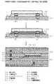
図1は本発明の原理的構成図であり、ここで図1を参照して、本発明における課題を解決するための手段を説明する。
図1参照
上記課題を解決するために、本発明は、電子部品1の接続端子2と多層回路基板3の内層回路4の接続電極5とを接続するとともに、電子部品1を覆うように多層配線構造8を設けた部品内蔵基板の製造方法において、接続端子2と接続電極5との間に平均粒径が50nm〜200nmのナノ粒径の金属粒子6を介在させる工程と、金属粒子6を焼結させて接続端子2と接続電極5との電気的接続を得る工程とを有することを特徴とする。FIG. 1 is a block diagram showing the principle of the present invention, and means for solving the problems in the present invention will be described with reference to FIG.
1, in order to solve the above-described problem, the present invention connects the
このように、金属粒子6を用いてフリップチップボンディングすることによって、低荷重且つ低温での接合が可能になるため、半導体素子と多層回路基板3の内層回路4間のクリアランスを損なうことなく確実な電気的接続が可能になり、それによって、部品内蔵基板の高密度実装化と信頼性の向上が可能になる。 As described above, since the flip chip bonding using the
この場合の金属粒子6としては、Agからなる金属粒子6或いは接続端子2及び接続電極5の少なくとも一方と合金化する金属粒子6、例えば、Sn、Bi、Zn、Ni、Inの内の少なくとも一種類の金属からなる金属粒子6を使用することが、低温における接合のために必要になる。 In this case, the
また、上述の金属粒子6を用いた場合には、金属粒子6を焼結させる工程における焼結温度を250℃以下にしても接合が可能になる。
即ち、ナノサイズの金属粒子6を用いた場合には、その金属の融点以下で金属粒子間がセラミックのように焼結して、バルクに近い状態になるため、低温での結合が可能になる。Further, when the
That is, when nano-sized
例えば、Agナノ粒子を用いた場合には、Agの融点960.8℃に対して200℃での接合が可能になり、荷重を与えなくても良好な電気的接触状態を実現することができる。
なお、ミクロンサイズのAgフィラーを用いた場合には、接続端子2の下に補足されたAgフィラーに高荷重をかけてAgフィラー間の接触面積を大きくしなければ良好な接触状態を確保することができない。For example, when Ag nanoparticles are used, bonding at 200 ° C. is possible with respect to the melting point of Ag of 960.8 ° C., and a good electrical contact state can be realized without applying a load. .
When a micron-sized Ag filler is used, a good contact state should be ensured unless a high load is applied to the Ag filler captured under the
この場合、金属粒子6を接続端子2と接続電極5との間に介在させる方法としては、金属粒子6を合成樹脂中に分散させた材料を接続端子2に転写することが最も典型的な方法であり、多層回路基板3の内層回路4上に特別な処理を施すことなく、ファインピッチの接続端子2に対して均一な量の金属粒子6の供給が可能になる。 In this case, the most typical method for interposing the
また、このように、金属粒子6をエポキシ樹脂等の合成樹脂に分散させることによって、金属が焼結したときの材料強度だけでなく、合成樹脂が硬化したときの強度を加えることにより、接合強度を上げることが可能となる。 In addition, by dispersing the
また、アンダーフィル樹脂を設ける工程としては、接続端子2と接続電極5とを接続した後に、電子部品1と多層回路基板3との間に封止用の合成樹脂を注入する工程でも良く、樹脂封止工程が簡単になる。 The step of providing the underfill resin may be a step of injecting a synthetic resin for sealing between the
或いは、接続端子2と接続電極5とを接続する前に、多層回路基板3上に封止用の合成樹脂を予め形成しておき、接続端子2を金属粒子6を介して接続電極5に圧接させたのち、接続端子2と接続電極5との接続及び合成樹脂の硬化とを同時的に行う工程であっても良い。 Alternatively, before connecting the
この場合、封止樹脂7の硬化工程において発生する電子部品1と多層回路基板3の内層回路4の熱膨張係数の差から生じる接合部に加わる応力を封止樹脂7内に分散させ、接続端子2の破断が生ずることがないので、接合信頼性を向上することができる。 In this case, the stress applied to the joint resulting from the difference in thermal expansion coefficient between the
また、電子部品1を覆う多層回路構造を形成するためには、アンダーフィル樹脂となる合成樹脂を硬化させたのち、プリプレグを用いて電子部品1を覆うように、内層回路4と電気的に接続する多層配線構造8を形成することが望ましい。 Further, in order to form a multilayer circuit structure covering the
上述の部品内蔵基板の製造方法を用いて部品内蔵基板を製造することによって、信頼性の高い高実装密度の部品内蔵基板の実現が可能になる。 By manufacturing the component-embedded substrate using the above-described method for manufacturing a component-embedded substrate, it is possible to realize a component-embedded substrate with high reliability and high mounting density.
本発明によれば、低荷重で接合を行っても、Auスタッドバンプと多層回路基板の内層回路電極は、良好な接合状態を維持でき、また、半導体素子等の電子部品と多層回路基板の内層回路間のクリアランスを確保できるため、部品内蔵基板の高信頼性化及び高密度実装化に寄与するところが大きい。 According to the present invention, even when bonding is performed with a low load, the Au stud bump and the inner layer circuit electrode of the multilayer circuit board can maintain a good bonding state, and an electronic component such as a semiconductor element and the inner layer of the multilayer circuit board can be maintained. Since the clearance between the circuits can be secured, it greatly contributes to the high reliability and high density mounting of the component-embedded substrate.
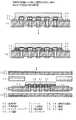
ここで、図2乃至図4を参照して、本発明の実施の形態における接合原理を説明する。
図2参照
まず、半導体チップ等の電子部品11に設けたAuスタッドバンプ12の先端に金属ナノ粒子14を含んだ接点材料13を設ける。
この場合の接点材料13はエポキシ樹脂等の合成樹脂15中に平均粒径が50nm〜200nmの金属ナノ粒子14を分散させたものであり、典型的には転写法によってAuスタッドバンプ12の先端に付着させる。Here, with reference to FIG. 2 thru | or FIG. 4, the joining principle in embodiment of this invention is demonstrated.
See Figure 2
First, the contact material 13 including the
In this case, the contact material 13 is obtained by dispersing
また、金属ナノ粒子14としては、Agナノ粒子或いはSnナノ粒子が典型的なものであるが、Ag、Sn以外にBi、Zn、Ni、或いはInからなる金属ナノ粒子を用いても良く、さらには、Ag−Snナノ粒子等のそれらの合金ナノ粒子を用いても良いものである。 The
次いで、先端に接点材料13を付着させたAuスタッドバンプ12を多層回路基板21の内層回路に設けたCu層、又は、Cu層/Ni/Au構造(表面がAu)のバンプ電極22に圧接させたのち、250℃以下で金属ナノ粒子14同士を溶融接合させる。 Next, the
この時、Cu層/Ni/Au構造(表面がAu)のバンプ電極22に対してSn等のAuとの合金化が可能な金属ナノ粒子14を用いた場合には、Auスタッドバンプ12及びバンプ電極22の表面のAu層との間でAuSn合金等の合金化により接合が行われることになる。
また、Cu層/Ni/Au構造(表面がAu)のバンプ電極22の代わりにCu層からなるバンプ電極を用いた場合も同様に、Sn等の合金化により接合が行われる。At this time, when
Similarly, when a bump electrode made of a Cu layer is used instead of the
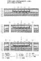
図3参照
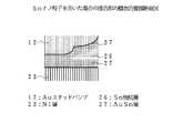
図3は、Agナノ粒子を用いた場合の接合部の概念的要部断面図であり、Auスタッドバンプ12とバンプ電極22を構成するAu層24との間にAgナノ粒子が焼結化したAg焼結層25が介在して良好な電気的接触状態を実現している。See Figure 3
FIG. 3 is a conceptual cross-sectional view of a joint portion using Ag nanoparticles, in which Ag nanoparticles are sintered between the
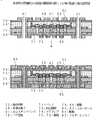
図4参照
図4は、Snナノ粒子を用いた場合の接合部の概念的要部断面図であり、Auスタッドバンプ12とバンプ電極22を構成するAu層24との間にSnナノ粒子が合金化したAuSn層27が形成され合金化により強固で良好な電気的接触状態を実現している。
なお、この場合、Auスタッドバンプ12の周辺部においては合金化せずに焼結化したSn焼結層26が存在する。See Figure 4
FIG. 4 is a conceptual cross-sectional view of a joint portion when Sn nanoparticles are used. AuSn in which Sn nanoparticles are alloyed between the
In this case, an Sn sintered layer 26 that is sintered without being alloyed is present in the peripheral portion of the
このような、接合を形成したのち、以降は、従来の部品内蔵基板の製造程度と同様にアンダーフィル樹脂を充填したのち、プリプレグを用いた多層配線基板の製造工程を利用して上部の多層配線構造を形成することによって部品内蔵基板が完成する。 After forming such a bond, after that, after filling the underfill resin in the same manner as the manufacturing of the conventional component-embedded substrate, the upper multilayer wiring using the manufacturing process of the multilayer wiring substrate using the prepreg is performed. A component-embedded substrate is completed by forming the structure.
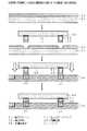
次に、図5及び図6を参照して本発明の実施例1の部品内蔵基板の製造工程を説明する。
図5参照
まず、平均粒径が50nm〜200nm、例えば、100nmのAgナノ粒子をエポキシ樹脂に分散させた接点材料32を転写ステージ31上に形成する。
この場合に、転写ステージ31にはスキージ(図示を省略)が取り付けられており、スキージと転写ステージ31のギャップを調整することにより、接点材料32の厚さを例えば、10μmとする。Next, the manufacturing process of the component built-in substrate according to the first embodiment of the present invention will be described with reference to FIGS.
See Figure 5
First, the
In this case, a squeegee (not shown) is attached to the transfer stage 31, and the thickness of the
次いで、接点材料32が未乾燥・未硬化の状態で半導体素子40を例えば、500gの荷重で転写ステージ31上に押しつけ、半導体素子40に設けたAuスタッドバンプ41の先端部に接点材料32を転写する。
なお、この場合の半導体素子40は、例えば、8.5mm角のサイズであり、また、Auスタッドバンプ41の高さは例えば、30μmであり、このAuスタッドバンプ41を例えば、50μmの間隔で680個形成している。Next, the
In this case, the
次いで、例えば、フリップチップボンダFCB−2M(パナソニックFSエンジニアリング製商品型番)を用いて、接点材料32を転写後の半導体素子40を厚さが0.35mmの多層回路基板の内層回路50に設けたCu/Ni/Au構造のパッド51と位置合わせし、次いで、250℃以下、例えば、200℃の加熱温度で、荷重2kgの条件で10秒間接合を行う。 Next, for example, by using a flip chip bonder FCB-2M (product model number manufactured by Panasonic FS Engineering), the
この時、上述のように、接点材料32中のAgナノ粒子同士が200℃の温度においてセラミックのように焼結して接合するとともに、接点材料32の母材となるエポキシ樹脂が硬化して接合をより強固なものにする。 At this time, as described above, the Ag nanoparticles in the
次いで、シアネート系の合成樹脂53、例えば、U8443(ナミックス製商品型番)を、例えば、60℃に加熱したホットプレート上で半導体素子40と内層回路50との間にシリンジ52を用いて注入する。 Next, a cyanate-based synthetic resin 53, for example, U8443 (Namics product model number) is injected between the
図6参照
次いで、恒温槽を用いて、例えば、150℃で2時間の加熱処理を行うことによって合成樹脂53を硬化させて封止樹脂54とする。See FIG.
Next, using a thermostatic bath, for example, heat treatment is performed at 150 ° C. for 2 hours to cure the synthetic resin 53 to obtain the sealing resin 54.
以降は、半導体素子40の実装部に対応する開口部を形成したプリプレグ55を介して、後で接続ビア56となる突起状の銀ペーストバンプを形成した内層回路50に、接続ビア、及び、配線パターンを形成した積層体を積層し、多層配線構造57を形成することによって、本発明の実施例1の部品内蔵基板が完成する。 Thereafter, via vias and
この実施例1の部品内蔵基板に対して、接合信頼性の試験として、接合信頼性試験項目である吸湿−リフロー性評価を模擬的に行う模擬吸湿リフロー試験を行った。
この模擬吸湿−リフローの評価方法は、実装後のサンプルを温度85℃、湿度85%、で12時間吸湿させた後、リフロー工程の最大温度である250℃にしたホットプレート上で2分間放置して、疑似吸湿−リフロー後の電気的導通の変化を測定した。A simulated moisture absorption reflow test was performed on the component-embedded substrate of Example 1 as a bonding reliability test in which a moisture absorption-reflow property evaluation, which is a bonding reliability test item, was simulated.
In this simulated moisture absorption-reflow evaluation method, the mounted sample is absorbed at a temperature of 85 ° C. and a humidity of 85% for 12 hours, and then left on a hot plate at 250 ° C. which is the maximum temperature of the reflow process for 2 minutes. The change in electrical continuity after pseudo moisture absorption and reflow was measured.
このときの合否判定は、導通抵抗の上昇率が5%以下の場合を合格としたが、実施例1の部品内蔵基板の場合には、サンプル数を50とした場合に、導通抵抗の上昇率が5%以下であり、良好な接合信頼性が得られた。 In the pass / fail judgment at this time, the case where the increase rate of the conduction resistance was 5% or less was accepted, but in the case of the component-embedded substrate of Example 1, the increase rate of the conduction resistance when the number of samples was 50. Was 5% or less, and good bonding reliability was obtained.
また、この実施例1の部品内蔵基板に対して、超音波映像装置FS200(日立建機ファインテック製商品型番)を用いて接合部の観察を行ったところ、各サンプルに接合部に剥離が観察されず、また、このときの半導体素子40と多層回路基板の内層回路50のクリアランスは約14μmであり、接合信頼性および半導体素子40と多層回路基板の内層回路50のクリアランスの確保が両立できた。 Moreover, when the joint part was observed with respect to the component built-in substrate of Example 1 using an ultrasonic imaging device FS200 (product model number manufactured by Hitachi Construction Machinery Finetech Co., Ltd.), peeling was observed at each joint part in each sample. In addition, the clearance between the
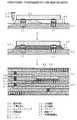
次に、図7及び図8を参照して本発明の実施例2の部品内蔵基板の製造工程を説明する。
図7参照
まず、実施例1と同様に、平均粒径が50nm〜200nm、例えば、100nmのSnナノ粒子をエポキシ樹脂に分散させた接点材料32を転写ステージ31上に形成する。
この場合に、転写ステージ31にはスキージ(図示を省略)が取り付けられており、スキージと転写ステージ31のギャップを調整することにより、接点材料32の厚さを例えば、10μmとする。Next, the manufacturing process of the component built-in substrate according to the second embodiment of the present invention will be described with reference to FIGS.
See FIG.
First, similarly to Example 1, a
In this case, a squeegee (not shown) is attached to the transfer stage 31, and the thickness of the
次いで、接点材料32が未乾燥・未硬化の状態で半導体素子40を例えば、500gの荷重で転写ステージ31上に押しつけ、半導体素子40に設けたAuスタッドバンプ41の先端部に接点材料32を転写する。
なお、この場合の半導体素子40は、例えば、8.5mm角のサイズであり、また、Auスタッドバンプ41の高さは例えば、30μmであり、このAuスタッドバンプ41を例えば、50μmの間隔で680個形成している。Next, the
In this case, the
次いで、例えば、120℃で予備加熱処理することによって、転写した接点材料中の溶剤成分を除去するとともに、Snナノ粒子の仮焼成を行う。 Next, for example, by preheating at 120 ° C., the solvent component in the transferred contact material is removed, and Sn nanoparticles are pre-fired.
次いで、例えば、塗布機FAD320s(武蔵エンジニアリング製商品型番)を用いて、例えば、厚さが0.2mmの多層回路基板の内層回路60上に封止樹脂となる合成樹脂62、例えば、UFR107(ナガセケムテックス製商品型番)を例えば、100μmの厚さに塗布し、フリップチップボンダ、例えば、FCB−2M(パナソニックFSエンジニアリング製商品型番)を用いて、転写後の半導体素子40のAuスタッドバンプ41を内層回路60に設けたCu/Ni/Au構造のパッド61と位置合わせする。 Next, for example, using a coating machine FAD320s (product model number manufactured by Musashi Engineering), for example, a synthetic resin 62 that becomes a sealing resin on the
図8参照
次いで、加熱温度200℃、荷重2kgの条件で10秒間接合を行う。
この時、接点材料32は120℃における予備加熱により溶剤成分が除去されており、また、Snナノ粒子も仮焼成されているので、荷重2kgで押圧した際に、塗布されている合成樹脂62をパッド61上から押し出す際に、接点材料32が押し出されることがなく、接点材料32中のSnナノ粒子同士の接合を介してパッド61とAuスタッドバンプ41が接合されるとともに、接点材料32の母材となるエポキシ樹脂が硬化して接合をより強固なものにする。See FIG.
Next, bonding is performed for 10 seconds under the conditions of a heating temperature of 200 ° C. and a load of 2 kg.
At this time, since the solvent component is removed from the
次いで、恒温槽を用いて、例えば、150℃で2時間の加熱処理を行うことによって合成樹脂62を硬化させて封止樹脂63とする。 Next, using a thermostat, for example, heat treatment is performed at 150 ° C. for 2 hours to cure the synthetic resin 62 to obtain the sealing resin 63.
以降は、半導体素子40の実装部に対応する開口部を形成したプリプレグ64を介して、後で接続ビア65となる突起状の銀ペーストバンプを形成した内層回路60に、接続ビア、及び、配線パターンを形成した積層体を積層し、多層配線構造66を形成することによって、本発明の実施例2の部品内蔵基板が完成する。 Thereafter, the connection vias and the wirings are connected to the
この実施例2においては、封止樹脂63の硬化工程において発生する半導体素子40と多層回路基板の内層回路60の熱膨張係数の差から生じる接合部に加わる応力を封止樹脂63内に分散させることができ、それによって、Auスタッドバンプ41の破断が生ずることがないので、接合信頼性をさらに向上することができる。 In the second embodiment, the stress applied to the joint caused by the difference in thermal expansion coefficient between the
この実施例2の部品内蔵基板に対して、上述の模擬吸湿リフロー試験を行ったところ、サンプル数を50とした場合に、実施例2の部品内蔵基板における導通抵抗の上昇率は5%以下であり、良好な接合信頼性が得られていることが確認された。 When the simulated moisture absorption reflow test was performed on the component-embedded substrate of Example 2, the increase rate of the conduction resistance in the component-embedded substrate of Example 2 was 5% or less when the number of samples was 50. It was confirmed that good bonding reliability was obtained.
また、この実施例2の部品内蔵基板に対して、上述の超音波映像装置による接合部の観察を行ったところ、各サンプルの接合部に剥離が観察されず、また、このときの半導体素子40と多層回路基板の内層回路60のクリアランスは約14μmであり、接合信頼性および半導体素子40と多層回路基板の内層回路60のクリアランスの確保が両立できた。 Further, when the joint portion of the component built-in substrate of Example 2 was observed by the above-described ultrasonic imaging apparatus, no peeling was observed at the joint portion of each sample, and the
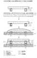
次に、図9乃至図12を参照して本発明の実施例3の部品内蔵基板の製造工程を説明する。
図9参照
まず、実施例1と同様に、平均粒径が50nm〜200nm、例えば、150nmのAgナノ粒子をエポキシ樹脂に分散させた接点材料32を転写ステージ31上に形成する。
この場合に、転写ステージ31にはスキージ(図示を省略)が取り付けられており、スキージと転写ステージ31のギャップを調整することにより、接点材料32の厚さを例えば、10μmとする。Next, a manufacturing process of the component built-in substrate according to the third embodiment of the present invention will be described with reference to FIGS.
Refer to FIG. 9 First, as in Example 1, a
In this case, a squeegee (not shown) is attached to the transfer stage 31, and the thickness of the
次いで、接点材料32が未乾燥・未硬化の状態で半導体素子40を例えば、500gの荷重で転写ステージ31上に押しつけ、半導体素子40に設けたAuスタッドバンプ41の先端部に接点材料32を転写する。
なお、この場合の半導体素子40は、例えば、8.5mm角のサイズであり、また、Auスタッドバンプ41の高さは例えば、30μmであり、このAuスタッドバンプ41を例えば、50μmの間隔で680個形成している。Next, the
In this case, the
次いで、例えば、120℃で予備加熱処理することによって、転写した接点材料中の溶剤成分を除去するとともに、Agナノ粒子の仮焼成を行う。 Next, for example, by preheating at 120 ° C., the solvent component in the transferred contact material is removed, and the Ag nanoparticles are temporarily fired.
次いで、例えば、塗布機FAD320s(武蔵エンジニアリング製商品型番)を用いて、例えば、厚さが0.2mmの多層回路基板を構成するコア基板70上に封止樹脂となる合成樹脂72、例えば、UFR107(ナガセケムテックス製商品型番)を例えば、100μmの厚さに塗布し、フリップチップボンダ、例えば、FCB−2M(パナソニックFSエンジニアリング製商品型番)を用いて、転写後の半導体素子40のAuスタッドバンプ41をコア基板70に設けたCuからなるパッド71と位置合わせする。 Next, for example, using a coating machine FAD320s (product model number manufactured by Musashi Engineering Co., Ltd.), for example, a synthetic resin 72 serving as a sealing resin on the
図10参照
次いで、加熱温度200℃、荷重2kgの条件で10秒間接合を行う。
この時、接点材料32は120℃における予備加熱により溶剤成分が除去されており、また、Agナノ粒子も仮焼成されているので、荷重2kgで押圧した際に、塗布されている合成樹脂72をパッド71上から押し出す際に、接点材料32が押し出されることがなく、接点材料32中のAgナノ粒子同士の接合を介してパッド71とAuスタッドバンプ41が接合されるとともに、接点材料32の母材となるエポキシ樹脂が硬化して接合をより強固なものにする。See FIG.
Next, bonding is performed for 10 seconds under the conditions of a heating temperature of 200 ° C. and a load of 2 kg.
At this time, since the solvent component is removed from the
次いで、恒温槽を用いて、例えば、150℃で2時間の加熱処理を行うことによって合成樹脂72を硬化させて封止樹脂73とする。 Next, using a thermostatic bath, for example, heat treatment is performed at 150 ° C. for 2 hours to cure the synthetic resin 72 to obtain a sealing
次いで、半導体素子40の実装部に対応する開口部を形成したプリプレグ74を介して、両側から銅箔77,78に樹脂79,80を付着させた樹脂付き銅箔75,76を積層する。 Subsequently, resin-coated copper foils 75 and 76 in which resins 79 and 80 are attached to the copper foils 77 and 78 are laminated from both sides through a
図11参照
次いで、樹脂79,80を硬化させる。
次いで、次に、ドリルを用いてスルーホール81,82を形成したのち、無電解Cuメッキ及び電解Cuメッキを用いて、スルーホール81,82にメッキを施すとともに、銅箔77,78の表面にもメッキを施してCuメッキ層83を形成する。See FIG.
Next, the
Next, after forming the through
図12参照
次いで、レジストパターン(図示は省略)を用いて、Cuメッキ層83及び銅箔77,78を所定形状にエッチングすることによって配線84を形成する。
最後にソルダーレジスト85を形成することによって、本発明の実施例3の部品内蔵基板が完成する。See FIG.
Next, the
Finally, by forming the solder resist 85, the component built-in substrate of Example 3 of the present invention is completed.
この実施例3においては、封止樹脂73の硬化工程において発生する半導体素子40と多層回路基板のコア基板70の熱膨張係数の差から生じる接合部に加わる応力を封止樹脂73内に分散させることができ、それによって、Auスタッドバンプ41の破断が生ずることがないので、接合信頼性をさらに向上することができる。 In the third embodiment, the stress applied to the joint portion resulting from the difference in thermal expansion coefficient between the
この実施例3の部品内蔵基板に対して、上述の模擬吸湿リフロー試験を行ったところ、サンプル数を50とした場合に、実施例3の部品内蔵基板における導通抵抗の上昇率は5%以下であり、良好な接合信頼性が得られていることが確認された。 When the above simulated moisture absorption reflow test was performed on the component-embedded substrate of Example 3, when the number of samples was 50, the increase rate of the conduction resistance in the component-embedded substrate of Example 3 was 5% or less. It was confirmed that good bonding reliability was obtained.
また、この実施例3の部品内蔵基板に対して、上述の超音波映像装置による接合部の観察を行ったところ、各サンプルの接合部に剥離が観察されず、また、このときの半導体素子40と多層回路基板のコア基板70のクリアランスは約15μmであり、接合信頼性および半導体素子40と多層回路基板のコア基板70のクリアランスの確保が両立できた。 Further, when the joint portion of the component built-in substrate of Example 3 was observed by the above-described ultrasonic imaging apparatus, no peeling was observed at the joint portion of each sample, and the
次に、本発明の効果を確認するための比較実験を行ったので説明する。
〔比較例1〕
この比較例1においては、フリップチップボンディング工程において、Auスタッドバンプに荷重をかけると同時に、接着剤の硬化を行う圧接方式を用いた。
具体的には、実施例1と同様の部材を用いて、塗布機FAD320s(武蔵エンジニアリング製商品型番)を用いて、厚さ0.35mmの多層回路基板の内層回路上に封止樹脂UFR107(ナガセケムテックス製商品型番)を塗布し、フリップチップボンダFCB−2M(パナソニックFSエンジニアリング製商品型番)を用いて、半導体素子を位置合わせした後、加熱温度200℃、荷重2kgで10秒間接合を行い、最後に恒温槽を用いて150℃で2時間硬化させた。Next, a comparative experiment for confirming the effect of the present invention will be described.
[Comparative Example 1]
In this comparative example 1, in the flip chip bonding process, a pressure contact method in which a load is applied to the Au stud bump and at the same time the adhesive is cured is used.
Specifically, using the same member as in Example 1, using a coating machine FAD320s (product model number manufactured by Musashi Engineering), a sealing resin UFR107 (Nagase) is formed on the inner layer circuit of a multilayer circuit board having a thickness of 0.35 mm. After applying the Chemtex product model) and aligning the semiconductor elements using the flip chip bonder FCB-2M (Panasonic FS Engineering product model number), bonding is performed for 10 seconds at a heating temperature of 200 ° C. and a load of 2 kg. Finally, it was cured at 150 ° C. for 2 hours using a thermostatic bath.
この比較例1の部品内蔵基板に対して、上述の模擬吸湿リフロー試験を行ったところ、50サンプル中28サンプルが不良となった。 When the above simulated moisture absorption reflow test was performed on the component-embedded substrate of Comparative Example 1, 28 samples out of 50 samples were defective.
この比較例1の部品内蔵基板の不良サンプルを断面研磨し、観察した結果、Auスタッドバンプと多層回路基板の内層回路電極の接触部に浮きが見られた。
これは、Auスタッドバンプの潰れ量が少なかったため、接合荷重不足により、接合部が断線したものと推測される。
また、このときの半導体素子と内層回路のクリアランスは平均で13μmであった。As a result of observing the cross section of the defective sample of the component built-in substrate of Comparative Example 1 and observing it, floating was observed at the contact portion between the Au stud bump and the inner layer circuit electrode of the multilayer circuit substrate.
This is presumed that the joining portion was disconnected due to insufficient joining load because the amount of collapse of the Au stud bump was small.
The clearance between the semiconductor element and the inner layer circuit at this time was 13 μm on average.
〔比較例2〕
また、比較例2においては、接合工程における荷重を8kgとした以外は、上述の比較例1と全く同じ条件で部品内蔵基板を作製した。
この比較例1の部品内蔵基板に対して、上述の模擬吸湿リフロー試験を行ったところ、50サンプル中3サンプルが不良となった。[Comparative Example 2]
In Comparative Example 2, a component-embedded substrate was produced under exactly the same conditions as in Comparative Example 1 except that the load in the joining process was 8 kg.
When the above simulated moisture absorption reflow test was performed on the component-embedded substrate of Comparative Example 1, 3 samples out of 50 samples were defective.
この比較例2の部品内蔵基板に対して、上述の超音波映像装置による接合部の観察を行ったところ、接合部の半導体素子中央部に剥離が観察された。
さらに、この接合サンプルを断面研磨し、SEM(走査型電子顕微鏡)を用いて観察した結果、接合部の中央は異物を起点とした剥離が生じていた。
また、この時の半導体素子と多層回路基板の内層回路のクリアランスは、4μmしかなかった。When the joint part was observed on the component-embedded substrate of Comparative Example 2 by the above-described ultrasonic imaging apparatus, peeling was observed at the central part of the semiconductor element of the joint part.
Furthermore, as a result of cross-polishing this bonded sample and observing it using an SEM (scanning electron microscope), the center of the bonded portion was peeled off starting from a foreign material.
At this time, the clearance between the semiconductor element and the inner circuit of the multilayer circuit board was only 4 μm.
以上の比較実験から明らかなように、同じ加圧条件及び加熱条件であっても、金属ナノ粒子を用いることによって接合部が焼結した金属或いは合金化した金属による金属間結合による接合が形成されるため、単なる、封止樹脂による圧接方式に比べてクリアランスを損なうことなく良好な電気的接触を実現することができる。 As is clear from the comparative experiment described above, even when the same pressure and heating conditions are used, the joint is formed by the metal-metal bond between the sintered metal or the alloyed metal by using the metal nanoparticles. Therefore, it is possible to realize good electrical contact without impairing the clearance as compared with a simple pressure welding method using a sealing resin.
また、接合に際しては過大の荷重をかける必要がないため、Auスタッドバンプが押し潰されて隣接するAuスタッドバンプと接触して短絡が発生することもないので、歩留り或いは信頼性が向上する。 Further, since it is not necessary to apply an excessive load at the time of joining, the Au stud bump is crushed and does not contact with the adjacent Au stud bump to cause a short circuit, so that the yield or reliability is improved.
以上、本発明の各実施例を説明してきたが、本発明は各実施例に記載された構成・条件等に限られるものではなく各種の変更が可能であり、例えば、上記半導体チップのサイズ或いはAuスタッドバンプのサイズ及びピッチは単なる一例であり、各種のサイズの半導体チップに適用されるものである。 Although the embodiments of the present invention have been described above, the present invention is not limited to the configurations and conditions described in the embodiments, and various modifications are possible. For example, the size of the semiconductor chip or The size and pitch of the Au stud bumps are merely examples, and are applied to semiconductor chips of various sizes.
また、上記の各実施例においては、接点材料を構成する金属ナノ粒子としてAgナノ粒子を用いているが、Agナノ粒子に限られるものではなく、Snナノ粒子を用いても良いものであり、この場合には、Auと合金化するので、Auスタッドバンプ及びパッドの表面のAu層と合金化して接合が強固になる。 In each of the above embodiments, Ag nanoparticles are used as the metal nanoparticles constituting the contact material. However, the present invention is not limited to Ag nanoparticles, and Sn nanoparticles may be used. In this case, since it is alloyed with Au, it is alloyed with the Au layer on the surface of the Au stud bump and the pad, thereby strengthening the bonding.
また、金属ナノ粒子は、Ag、Snに限られるものではなく、Bi、Zn、Ni或いはInからなるナノ粒子を用いても良いものであり、さらには、Ag−Sn合金ナノ粒子等のこれらの金属の合金ナノ粒子を用いても良いものである。 In addition, the metal nanoparticles are not limited to Ag and Sn, and nanoparticles made of Bi, Zn, Ni, or In may be used. Furthermore, these Ag-Sn alloy nanoparticles and the like may be used. Metal alloy nanoparticles may also be used.
また、上記の各実施例においては、接点材料の転写工程において、接点材料が未乾燥・未硬化の状態で行っているが、予めプリベークにより、例えば、120℃のプリベークにより半乾燥・予備焼結した状態転写を行っても良いものである。 Further, in each of the above embodiments, the contact material is transferred in an undried and uncured state in the contact material transfer step, but is pre-baked, for example, pre-baked at 120 ° C. and semi-dried / pre-sintered The transferred state may be performed.
ここで、再び、図1を参照して、本発明の詳細な特徴を改めて説明する。
再び、図1参照
(付記1) 電子部品1の接続端子2と多層回路基板3の内層回路の接続電極5とを接続するとともに、前記電子部品1を覆うように多層配線構造8を設けた部品内蔵基板の製造方法において、前記接続端子2と前記接続電極5との間に平均粒径が50nm〜200nmのナノ粒径の金属粒子6を介在させる工程と、前記金属粒子6を焼結させて前記接続端子2と前記接続電極5との電気的接続を得る工程とを有することを特徴とする部品内蔵基板の製造方法。
(付記2) 上記金属粒子6として、上記接続端子2及び接続電極5の少なくとも一方と合金化する金属粒子6を使用することを特徴とする付記1記載の部品内蔵基板の製造方法。
(付記3) 上記金属粒子6が、Ag、Sn、Bi、Zn、Ni、Inの内の少なくとも一種類の金属からなることを特徴とする付記1または2に記載の部品内蔵基板の製造方法。
(付記4) 上記金属粒子6を焼結させる工程における焼結温度が250℃以下であることを特徴とする付記1乃至3のいずれか1に記載の部品内蔵基板の製造方法。
(付記5) 上記金属粒子6を上記接続端子2と上記接続電極5との間に介在させる工程において、前記金属粒子6を合成樹脂中に分散させた材料を前記接続端子2に転写することを特徴とする付記1乃至4のいずれか1に記載の部品内蔵基板の製造方法。
(付記6) 上記接続端子2と上記接続電極5とを接続した後に、上記電子部品1と上記多層回路基板3との間に封止用の合成樹脂を注入する工程を有することを特徴とする付記1乃至3のいずれか1に記載の部品内蔵基板の製造方法。
(付記7) 上記接続端子2と上記接続電極5とを接続する前に、上記多層回路基板3上に封止用の合成樹脂を予め形成しておき、前記接続端子2を上記金属粒子6を介して前記接続電極5に圧接させたのち、前記接続端子2と前記接続電極5との接続及び前記合成樹脂の硬化とを同時的に行うことを特徴とする付記1乃至3のいずれか1に記載の部品内蔵基板の製造方法。
(付記8) 上記合成樹脂を硬化させたのち、プリプレグを用いて上記電子部品1を覆うように、上記内層回路と電気的に接続する多層配線構造8を形成する工程を有することを特徴とする付記1乃至5のいずれか1に記載の部品内蔵基板の製造方法。
(付記9) 付記1乃至8のいずれか1に記載の部品内蔵基板の製造方法を用いて製造された部品内蔵基板。Here, the detailed features of the present invention will be described again with reference to FIG.
Again see Figure 1
(Supplementary Note 1) A method of manufacturing a component-embedded board in which the
(Additional remark 2) The
(Additional remark 3) The said
(Additional remark 4) The sintering temperature in the process of sintering the said
(Supplementary Note 5) In the step of interposing the
(Additional remark 6) It has the process of inject | pouring the synthetic resin for sealing between the said
(Appendix 7) Before connecting the
(Additional remark 8) It has the process of forming the
(Additional remark 9) The component built-in board manufactured using the manufacturing method of the component built-in board of any one of
本発明の活用例としては、半導体集積回路チップを内蔵した部品内蔵基板が典型的なものであるが、内蔵される電子部品は半導体集積回路チップに限られるものではなく、L,C,R等の受動部品でも良く、或いは、薄膜SAWデバイス等でも良く、内蔵される電子部品は限定されないものである。 As a practical example of the present invention, a component-embedded substrate incorporating a semiconductor integrated circuit chip is typical, but the built-in electronic component is not limited to a semiconductor integrated circuit chip, and L, C, R, etc. The passive component may be a thin film SAW device or the like, and the built-in electronic component is not limited.
1 電子部品
2 接続端子
3 多層回路
4 内層回路
5 接続電極
6 金属粒子
7 封止樹脂
8 多層配線構造
11 電子部品
12 Auスタッドバンプ
13 接点材料
14 金属ナノ粒子
15 合成樹脂
21 多層回路基板
22 バンプ電極
23 Ni層
24 Au層
25 Ag焼結層
26 Sn焼結層
27 AuSn層
31 転写ステージ
32 接点材料
40 半導体素子
41 Auスタッドバンプ
50 内層回路
51 パッド
52 シリンジ
53 合成樹脂
54 封止樹脂
55 プリプレグ
56 接続ビア
57 多層配線構造
60 内層回路
61 パッド
62 合成樹脂
63 封止樹脂
64 プリプレグ
65 接続ビア
66 多層配線構造
70 コア基板
71 パッド
72 合成樹脂
73 封止樹脂
74 プリプレグ
75,76 樹脂付き銅箔
77,78 銅箔
79,80 樹脂
81,82 スルーホール
83 Cuメッキ層
84 配線
85 ソルダーレジストDESCRIPTION OF
Claims (5)
Translated fromJapanesePriority Applications (1)
| Application Number | Priority Date | Filing Date | Title |
|---|---|---|---|
| JP2007083397AJP2008244191A (en) | 2007-03-28 | 2007-03-28 | Manufacturing method of component-embedded substrate |
Applications Claiming Priority (1)
| Application Number | Priority Date | Filing Date | Title |
|---|---|---|---|
| JP2007083397AJP2008244191A (en) | 2007-03-28 | 2007-03-28 | Manufacturing method of component-embedded substrate |
Publications (1)
| Publication Number | Publication Date |
|---|---|
| JP2008244191Atrue JP2008244191A (en) | 2008-10-09 |
Family
ID=39915155
Family Applications (1)
| Application Number | Title | Priority Date | Filing Date |
|---|---|---|---|
| JP2007083397APendingJP2008244191A (en) | 2007-03-28 | 2007-03-28 | Manufacturing method of component-embedded substrate |
Country Status (1)
| Country | Link |
|---|---|
| JP (1) | JP2008244191A (en) |
Cited By (4)
| Publication number | Priority date | Publication date | Assignee | Title |
|---|---|---|---|---|
| WO2010070103A1 (en)* | 2008-12-19 | 2010-06-24 | 3D Plus | Method for the collective production of electronic modules for surface mounting |
| JP2011228422A (en)* | 2010-04-19 | 2011-11-10 | Dainippon Printing Co Ltd | Wiring board incorporating components, and method of manufacturing the same |
| KR20140125417A (en)* | 2012-02-08 | 2014-10-28 | 크레인 일렉트로닉스, 아이엔씨. | Multilayer electronics assembly and method for embedding electrical circuit components within a three dimensional module |
| JP2019086485A (en)* | 2017-11-10 | 2019-06-06 | 株式会社豊田中央研究所 | Data acquisition device |
Citations (3)
| Publication number | Priority date | Publication date | Assignee | Title |
|---|---|---|---|---|
| JP2003174141A (en)* | 2001-09-27 | 2003-06-20 | Dt Circuit Technology Co Ltd | Semiconductor device and method for manufacturing the same |
| JP2004146731A (en)* | 2002-10-28 | 2004-05-20 | Mitsubishi Electric Corp | Method for manufacturing multilayer wiring substrate |
| JP2005302870A (en)* | 2004-04-08 | 2005-10-27 | Seiko Epson Corp | Electronic component manufacturing method, electronic component, electro-optical device, and electronic apparatus |
- 2007
- 2007-03-28JPJP2007083397Apatent/JP2008244191A/enactivePending
Patent Citations (3)
| Publication number | Priority date | Publication date | Assignee | Title |
|---|---|---|---|---|
| JP2003174141A (en)* | 2001-09-27 | 2003-06-20 | Dt Circuit Technology Co Ltd | Semiconductor device and method for manufacturing the same |
| JP2004146731A (en)* | 2002-10-28 | 2004-05-20 | Mitsubishi Electric Corp | Method for manufacturing multilayer wiring substrate |
| JP2005302870A (en)* | 2004-04-08 | 2005-10-27 | Seiko Epson Corp | Electronic component manufacturing method, electronic component, electro-optical device, and electronic apparatus |
Cited By (10)
| Publication number | Priority date | Publication date | Assignee | Title |
|---|---|---|---|---|
| WO2010070103A1 (en)* | 2008-12-19 | 2010-06-24 | 3D Plus | Method for the collective production of electronic modules for surface mounting |
| FR2940521A1 (en)* | 2008-12-19 | 2010-06-25 | 3D Plus | COLLECTIVE MANUFACTURING METHOD OF ELECTRONIC MODULES FOR SURFACE MOUNTING |
| US8359740B2 (en) | 2008-12-19 | 2013-01-29 | 3D Plus | Process for the wafer-scale fabrication of electronic modules for surface mounting |
| JP2011228422A (en)* | 2010-04-19 | 2011-11-10 | Dainippon Printing Co Ltd | Wiring board incorporating components, and method of manufacturing the same |
| KR20140125417A (en)* | 2012-02-08 | 2014-10-28 | 크레인 일렉트로닉스, 아이엔씨. | Multilayer electronics assembly and method for embedding electrical circuit components within a three dimensional module |
| JP2015508235A (en)* | 2012-02-08 | 2015-03-16 | クレーン エレクトロニクス、インコーポレーテッド | Multilayer electronic device assembly and method for embedding electrical circuit elements in a three-dimensional module |
| US9888568B2 (en) | 2012-02-08 | 2018-02-06 | Crane Electronics, Inc. | Multilayer electronics assembly and method for embedding electrical circuit components within a three dimensional module |
| KR102103196B1 (en) | 2012-02-08 | 2020-04-22 | 크레인 일렉트로닉스, 아이엔씨. | Multilayer electronics assembly and method for embedding electrical circuit components within a three dimensional module |
| US11172572B2 (en) | 2012-02-08 | 2021-11-09 | Crane Electronics, Inc. | Multilayer electronics assembly and method for embedding electrical circuit components within a three dimensional module |
| JP2019086485A (en)* | 2017-11-10 | 2019-06-06 | 株式会社豊田中央研究所 | Data acquisition device |
Similar Documents
| Publication | Publication Date | Title |
|---|---|---|
| US8390106B2 (en) | Circuit board with built-in semiconductor chip and method of manufacturing the same | |
| JP4731340B2 (en) | Manufacturing method of semiconductor device | |
| CN101156238B (en) | Protruding electrodes for connecting electronic components and method of manufacturing electronic component mounting body | |
| US7921551B2 (en) | Electronic component mounting method | |
| WO2001086716A1 (en) | Semiconductor device mounting circuit board, method of producing the same, and method of producing mounting structure using the same | |
| JPH09326419A (en) | Semiconductor element mounting method | |
| TWI461118B (en) | Electronic-component-mounted wiring substrate and method of manufacturing the same | |
| JP4846633B2 (en) | Manufacturing method of component-embedded substrate | |
| JP4509550B2 (en) | Relay board, relay board with semiconductor element, board with relay board, structure comprising semiconductor element, relay board and board | |
| KR20040100949A (en) | Method of manufacturing semiconductor package and method of manufacturing semiconductor device | |
| JP2012204631A (en) | Semiconductor device, semiconductor device manufacturing method and electronic apparatus | |
| US6657313B1 (en) | Dielectric interposer for chip to substrate soldering | |
| JP2005216696A (en) | Relay board and board with relay board | |
| JP4051570B2 (en) | Manufacturing method of semiconductor device | |
| JP2008244191A (en) | Manufacturing method of component-embedded substrate | |
| JP4065264B2 (en) | Substrate with relay substrate and method for manufacturing the same | |
| US20220071015A1 (en) | Circuit board structure and manufacturing method thereof | |
| JP2003152022A (en) | Adhesive member, semiconductor device and its manufacturing method, circuit board, and electronic equipment | |
| JP2001068604A (en) | Fixing resin, anisotropic conductive resin, semiconductor device and its manufacturing method, circuit board, and electronic equipment | |
| JP5323395B2 (en) | Electronic module and method for manufacturing electronic module | |
| JP3768870B2 (en) | Mounting method of semiconductor element | |
| JP4786914B2 (en) | Composite wiring board structure | |
| JP3704497B2 (en) | Circuit board, repair method and mounting structure | |
| JP2006310543A (en) | Wiring board and its production process, wiring board with semiconductor circuit element | |
| JP2005244163A (en) | Substrate with extension board and its manufacturing method |
Legal Events
| Date | Code | Title | Description |
|---|---|---|---|
| A621 | Written request for application examination | Free format text:JAPANESE INTERMEDIATE CODE: A621 Effective date:20091208 | |
| RD03 | Notification of appointment of power of attorney | Free format text:JAPANESE INTERMEDIATE CODE: A7423 Effective date:20110915 | |
| A977 | Report on retrieval | Free format text:JAPANESE INTERMEDIATE CODE: A971007 Effective date:20111031 | |
| A131 | Notification of reasons for refusal | Free format text:JAPANESE INTERMEDIATE CODE: A131 Effective date:20111108 | |
| A521 | Written amendment | Free format text:JAPANESE INTERMEDIATE CODE: A523 Effective date:20120105 | |
| A131 | Notification of reasons for refusal | Free format text:JAPANESE INTERMEDIATE CODE: A131 Effective date:20120710 | |
| A02 | Decision of refusal | Free format text:JAPANESE INTERMEDIATE CODE: A02 Effective date:20121113 |