JP2008241447A - Image reading apparatus and image reading method - Google Patents
Image reading apparatus and image reading methodDownload PDFInfo
- Publication number
- JP2008241447A JP2008241447AJP2007082090AJP2007082090AJP2008241447AJP 2008241447 AJP2008241447 AJP 2008241447AJP 2007082090 AJP2007082090 AJP 2007082090AJP 2007082090 AJP2007082090 AJP 2007082090AJP 2008241447 AJP2008241447 AJP 2008241447A
- Authority
- JP
- Japan
- Prior art keywords
- image
- light
- subject
- image sensor
- light receiving
- Prior art date
- Legal status (The legal status is an assumption and is not a legal conclusion. Google has not performed a legal analysis and makes no representation as to the accuracy of the status listed.)
- Pending
Links
Images


Classifications
- G—PHYSICS
- G01—MEASURING; TESTING
- G01N—INVESTIGATING OR ANALYSING MATERIALS BY DETERMINING THEIR CHEMICAL OR PHYSICAL PROPERTIES
- G01N21/00—Investigating or analysing materials by the use of optical means, i.e. using sub-millimetre waves, infrared, visible or ultraviolet light
- G01N21/62—Systems in which the material investigated is excited whereby it emits light or causes a change in wavelength of the incident light
- G01N21/63—Systems in which the material investigated is excited whereby it emits light or causes a change in wavelength of the incident light optically excited
- G01N21/64—Fluorescence; Phosphorescence
- G01N21/645—Specially adapted constructive features of fluorimeters
- G01N21/6456—Spatial resolved fluorescence measurements; Imaging
- G—PHYSICS
- G01—MEASURING; TESTING
- G01N—INVESTIGATING OR ANALYSING MATERIALS BY DETERMINING THEIR CHEMICAL OR PHYSICAL PROPERTIES
- G01N21/00—Investigating or analysing materials by the use of optical means, i.e. using sub-millimetre waves, infrared, visible or ultraviolet light
- G01N21/75—Systems in which material is subjected to a chemical reaction, the progress or the result of the reaction being investigated
- G01N21/77—Systems in which material is subjected to a chemical reaction, the progress or the result of the reaction being investigated by observing the effect on a chemical indicator
Landscapes
- Health & Medical Sciences (AREA)
- Chemical & Material Sciences (AREA)
- Physics & Mathematics (AREA)
- Pathology (AREA)
- Life Sciences & Earth Sciences (AREA)
- Analytical Chemistry (AREA)
- Biochemistry (AREA)
- General Health & Medical Sciences (AREA)
- General Physics & Mathematics (AREA)
- Immunology (AREA)
- Plasma & Fusion (AREA)
- Chemical Kinetics & Catalysis (AREA)
- Engineering & Computer Science (AREA)
- Nuclear Medicine, Radiotherapy & Molecular Imaging (AREA)
- Investigating, Analyzing Materials By Fluorescence Or Luminescence (AREA)
- Investigating Or Analysing Materials By The Use Of Chemical Reactions (AREA)
Abstract
Description
Translated fromJapanese本発明は、生体由来物質を含む被写体を撮影して前記生体由来物質の反応状況に応じた画像を取得する画像読取装置、及びその画像読取方法に関する。 The present invention relates to an image reading apparatus that captures an image of a subject including a biological substance and acquires an image corresponding to the reaction state of the biological substance, and an image reading method thereof.
筐体内に被写体を配置し、筐体内に備えられた光源で被写体を照射して被写体を撮影する装置が、従来より様々な分野で利用されている。生化学の分野においては、化学発光物質や蛍光物質を標識物質として使用し、これらの発光や蛍光を読み取ることによって、遺伝子配列、遺伝子の発現レベル、蛋白質の分離、同定、あるいは分子量、特性の評価などを行う撮影装置が、例えば、特許文献1などによって知られている。 2. Description of the Related Art Conventionally, apparatuses that place a subject in a housing and shoot the subject by irradiating the subject with a light source provided in the housing have been used in various fields. In the field of biochemistry, chemiluminescent substances and fluorescent substances are used as labeling substances, and by reading these luminescence and fluorescence, gene sequences, gene expression levels, protein separation and identification, or molecular weight and property evaluation For example, Japanese Patent Application Laid-Open No. H10-228688 discloses an imaging apparatus that performs the above.
具体的には、例えば、電気泳動させるべき複数のDNA断片を含む溶液の中に蛍光色素を加えた後、複数のDNA断片をゲル支持体上で電気泳動させる。あるいは、蛍光色素を含有させたゲル支持体上で複数のDNA断片を電気泳動させる。この後、蛍光色素を含んだ溶液にゲル支持体を浸すなどして、電気泳動されたDNA断片を標識する。そして、ゲル支持体に励起光を照射して蛍光色素を励起させ、生じた蛍光を検出することによって画像を生成する。このように生成した画像により、ゲル支持体上のDNA分布を検出することができる。 Specifically, for example, after adding a fluorescent dye into a solution containing a plurality of DNA fragments to be electrophoresed, the plurality of DNA fragments are electrophoresed on a gel support. Alternatively, a plurality of DNA fragments are electrophoresed on a gel support containing a fluorescent dye. Thereafter, the electrophoretic DNA fragment is labeled by immersing the gel support in a solution containing a fluorescent dye. Then, the gel support is irradiated with excitation light to excite the fluorescent dye, and the generated fluorescence is detected to generate an image. The DNA distribution on the gel support can be detected from the image thus generated.
あるいは、複数のDNA断片を、ゲル支持体上で電気泳動させた後に、DNAを変性し、次いで、サザン・ブロッティング法により、ニトロセルロースなどの転写支持体上に、変性DNA断片の少なくとも一部を転写し、目的とするDNAと相補的なDNAもしくはRNAを蛍光色素で標識して調製したプローブと変性DNA断片とをハイブリダイズさせ、プローブDNAもしくはプローブRNAと相補的なDNA断片のみを選択的に標識し、励起光によって蛍光色素を励起して、生じた蛍光を検出して画像を生成することにより、転写支持体上の目的とするDNA分布を検出することができる。
特許文献1の撮影装置では、ゲル支持体や転写支持体などといった被写体を光学系によってイメージセンサに結像することにより、発光画像や蛍光画像を取得している。しかしながら、化学発光や蛍光は、非常に微弱な光であるため、光学系にF値の小さい明るいレンズを用いたとしても、光学系を通る間に光が減衰してしまうという問題があった。このため、長時間露出を行わなければならないなど、光学系が、化学発光や蛍光の検出感度に悪影響を与えていた。 In the imaging apparatus of Patent Document 1, a luminescent image or a fluorescent image is acquired by forming an image of a subject such as a gel support or a transfer support on an image sensor using an optical system. However, since chemiluminescence and fluorescence are very weak light, there is a problem that even if a bright lens having a small F value is used in the optical system, the light is attenuated while passing through the optical system. For this reason, the optical system has had a bad influence on the detection sensitivity of chemiluminescence or fluorescence, such as having to perform exposure for a long time.
また、被写体は、位置ズレの防止や操作性などの観点から筐体内に水平に配置される。一方、光学系やイメージセンサは、この被写体と直交するように鉛直方向に設けられる。このため、被写体と光学系との間に所定のスペースが必要になり、こうしたスペースなどによって装置が背高になってしまうという問題もあった。近年では、様々な分野において装置の小型・軽量化が進められており、生化学の分野においても、よりコンパクトな装置の登場が望まれている。 In addition, the subject is horizontally arranged in the housing from the viewpoints of prevention of positional deviation and operability. On the other hand, the optical system and the image sensor are provided in the vertical direction so as to be orthogonal to the subject. For this reason, a predetermined space is required between the subject and the optical system, and there is a problem that the apparatus becomes tall due to such a space. In recent years, the size and weight of devices have been reduced in various fields, and the appearance of more compact devices is also desired in the field of biochemistry.
本発明は、上記課題を鑑みてなされたものであって、化学発光や蛍光の検出感度を向上させて短時間での露出を可能にするとともに、装置の薄型化を実現する画像読取装置を提供することを目的とする。 The present invention has been made in view of the above problems, and provides an image reading apparatus that improves chemiluminescence and fluorescence detection sensitivity, enables exposure in a short time, and realizes thinning of the apparatus. The purpose is to do.
上記課題を達成するため、本発明の画像読取装置は、生体由来物質を含む被写体を支持する支持面を有する支持台と、前記支持面を覆って遮光するカバーと、受光面から入射した光の光量に応じて電荷を発生させる有機光電変換膜を有し、前記受光面が前記支持面に露呈するように前記支持台に設けられ、前記受光面に前記被写体を乗せた状態で前記被写体の撮影を行うイメージセンサとを備えたことを特徴とする。 In order to achieve the above object, an image reading apparatus according to the present invention includes a support base having a support surface that supports a subject including a biological substance, a cover that covers the support surface and shields light, and light incident from the light receiving surface. An organic photoelectric conversion film that generates an electric charge according to the amount of light is provided on the support base so that the light receiving surface is exposed to the support surface, and the subject is photographed with the subject placed on the light receiving surface. And an image sensor for performing the above.
なお、前記支持面を覆った閉じ位置に前記カバーがある際に、前記受光面と対面して前記受光面に光を照射する光源を、前記カバーの内面に設けることが好ましい。 When the cover is in the closed position covering the support surface, it is preferable that a light source that faces the light receiving surface and emits light to the light receiving surface is provided on the inner surface of the cover.
また、前記光源は、前記受光面の全域に亘って均一な光量の光が照射されるように前記カバーの内面に複数設けられていることが好ましい。 Moreover, it is preferable that a plurality of the light sources are provided on the inner surface of the cover so that a uniform amount of light is irradiated over the entire area of the light receiving surface.
さらに、前記カバーが前記閉じ位置にある状態で前記光源を前記受光面と平行な方向に一定速度でスライド移動させることにより、前記受光面の全域に均一な光量の光を照射する光源移動手段を設けるようにしてもよい。 Further, a light source moving means for irradiating the entire light receiving surface with a uniform amount of light by sliding the light source at a constant speed in a direction parallel to the light receiving surface while the cover is in the closed position. You may make it provide.
なお、前記光源は、前記受光面に白色光を照射し、前記イメージセンサは、前記被写体を透過した前記白色光を撮影することが好ましい。 It is preferable that the light source irradiates the light receiving surface with white light, and the image sensor captures the white light transmitted through the subject.
また、前記イメージセンサが前記白色光を撮影した際に、前記イメージセンサが取得した画像データの各画素が飽和しているか否かを判定し、飽和している画素の出力値を所定の値に設定する画像処理手段を設けることが好ましい。 Further, when the image sensor captures the white light, it is determined whether or not each pixel of the image data acquired by the image sensor is saturated, and the output value of the saturated pixel is set to a predetermined value. It is preferable to provide image processing means for setting.
さらに、前記光源は、蛍光色素によって前記生体由来物質が標識された前記被写体を励起させる励起光を照射し、前記イメージセンサは、前記励起によって生じる蛍光を撮影するものとしてもよい。 Furthermore, the light source may emit excitation light that excites the subject labeled with the biological substance with a fluorescent dye, and the image sensor may photograph fluorescence generated by the excitation.
なお、前記イメージセンサを所定の温度に調節する温度調節手段を設けることが好ましい。この際、前記温度調節手段は、前記支持台の内部に形成される空洞部の天井面にアレイ状に配置される複数のペルチエ素子と温度センサとで構成されることが好適である。 It is preferable to provide a temperature adjusting means for adjusting the image sensor to a predetermined temperature. At this time, it is preferable that the temperature adjusting means includes a plurality of Peltier elements and temperature sensors arranged in an array on the ceiling surface of the hollow portion formed inside the support base.
また、前記イメージセンサは、感知する光の波長が異なる複数の前記有機光電変換膜を有することが好ましい。この際、前記各有機光電変換膜は、短い波長の光ほど先に感知されるように積層されていることが好適である。 The image sensor preferably includes a plurality of the organic photoelectric conversion films having different wavelengths of light to be sensed. At this time, the organic photoelectric conversion films are preferably laminated so that light having a shorter wavelength is sensed earlier.
また、前記イメージセンサは、前記有機光電変換膜を保護する保護膜を有することが好ましい。さらに、前記イメージセンサは、前記励起光の波長域のみをカットするフィルタを有することが好ましい。 The image sensor preferably has a protective film for protecting the organic photoelectric conversion film. Furthermore, it is preferable that the image sensor has a filter that cuts only the wavelength range of the excitation light.
なお、本発明の画像読取装置は、前記被写体を支持する支持面を有する支持台と、前記支持面を覆って遮光するカバーと、受光面から入射した光の光量に応じて電荷を発生させる有機光電変換膜を有し、前記支持面を覆う閉じ位置に前記カバーがある際に、前記支持面上の前記被写体に前記受光面が接触するように前記カバーの内面に設けられ、前記受光面に前記被写体を接触させた状態で前記被写体の撮影を行うイメージセンサとを備えるものであってもよい。この場合、前記カバーが前記閉じ位置にある際に、前記受光面と対面して前記受光面に光を照射する光源を、前記支持台に設けることが好ましい。 The image reading apparatus according to the present invention includes a support base having a support surface that supports the subject, a cover that covers and shields the support surface, and an organic that generates an electric charge according to the amount of light incident from the light receiving surface. The photoelectric conversion film is provided on the inner surface of the cover so that the light receiving surface comes into contact with the subject on the support surface when the cover is in a closed position that covers the support surface. And an image sensor that captures an image of the subject while the subject is in contact with the subject. In this case, when the cover is in the closed position, a light source that faces the light receiving surface and emits light to the light receiving surface is preferably provided on the support base.
また、本発明の画像読取装置は、前記被写体を支持する支持面を有する支持台と、前記支持面を覆って遮光するカバーと、受光面から入射した光の光量に応じて電荷を発生させる有機光電変換膜を有し、前記受光面が前記支持面に露呈するように前記支持台に設けられ、前記受光面に前記被写体を乗せた状態で前記被写体の撮影を行う第1イメージセンサと、受光面から入射した光の光量に応じて電荷を発生させる有機光電変換膜を有し、前記支持面を覆う閉じ位置に前記カバーがある際に、前記支持面上の前記被写体に前記受光面が接触するように前記カバーの内面に設けられ、前記受光面に前記被写体を接触させた状態で前記被写体の撮影を行う第2イメージセンサとを備えるものであってもよい。 Further, the image reading apparatus of the present invention includes a support base having a support surface that supports the subject, a cover that covers and shields the support surface, and an organic that generates an electric charge according to the amount of light incident from the light receiving surface. A first image sensor having a photoelectric conversion film, provided on the support base such that the light receiving surface is exposed to the support surface, and photographing the subject with the subject placed on the light receiving surface; An organic photoelectric conversion film that generates an electric charge according to the amount of light incident from the surface, and the light receiving surface contacts the subject on the support surface when the cover is in a closed position that covers the support surface The second image sensor may be provided on the inner surface of the cover so as to photograph the subject in a state where the subject is in contact with the light receiving surface.
この場合、前記第1イメージセンサが取得したアナログの第1画像データと前記第2イメージセンサが取得したアナログの第2画像データとのそれぞれをデジタルの画像データに変換するA/Dコンバータと、前記A/Dコンバータが変換したデジタルの各画像データを合成して1つの合成画像データを作成する画像合成手段とを設けることが好ましい。 In this case, an A / D converter that converts each of the analog first image data acquired by the first image sensor and the analog second image data acquired by the second image sensor into digital image data; It is preferable to provide image composition means for synthesizing digital image data converted by the A / D converter to create one composite image data.
また、前記第1イメージセンサが取得したアナログの第1画像データと前記第2イメージセンサが取得したアナログの第2画像データとを合成して1つの合成画像データを作成する画像合成手段と、前記画像合成手段が作成したアナログの前記合成画像データをデジタルの画像データに変換するA/Dコンバータとを設けるようにしてもよい。 An image combining unit configured to combine the analog first image data acquired by the first image sensor and the analog second image data acquired by the second image sensor to generate one composite image data; You may make it provide the A / D converter which converts the said analog synthetic | combination image data which the image synthetic | combination means produced into digital image data.
なお、本発明の画像読取方法は、生体由来物質を含む被写体を支持する支持面を有する支持台と、前記支持面を覆って遮光するカバーと、受光面から入射した光の光量に応じて電荷を発生させる有機光電変換膜を有し、前記支持台と前記カバーとの少なくとも一方に設けられるイメージセンサとを備え、前記イメージセンサで前記被写体を撮影して前記被写体に含まれる前記生体由来物質の反応状況に応じた画像を取得する画像読取装置において、前記受光面を前記被写体に直接接触させた状態で撮影を行うことを特徴とする。 Note that the image reading method of the present invention includes a support base having a support surface that supports a subject containing a biological substance, a cover that covers and shields the support surface, and charges according to the amount of light incident from the light receiving surface. And an image sensor provided on at least one of the support base and the cover. The image sensor is used to photograph the subject and the biological substance contained in the subject. In the image reading apparatus for acquiring an image according to a reaction state, photographing is performed in a state where the light receiving surface is in direct contact with the subject.
この際、前記イメージセンサを所定の温度に調節しながら撮影を行うことが好ましい。また、前記イメージセンサには、近赤外線の光を感知する前記有機光電変換膜と、赤色の光を感知する前記有機光電変換膜と、緑色の光を感知する前記有機光電変換膜と、青色の光を感知する前記有機光電変換膜とが設けられており、前記各有機光電変換膜のそれぞれで近赤外線、赤色、緑色、青色の画像を個別に取得することが好ましい。 At this time, it is preferable to perform photographing while adjusting the image sensor to a predetermined temperature. The image sensor includes the organic photoelectric conversion film that senses near-infrared light, the organic photoelectric conversion film that senses red light, the organic photoelectric conversion film that senses green light, and a blue color. It is preferable that the organic photoelectric conversion film that senses light is provided, and near-infrared, red, green, and blue images are individually acquired in each of the organic photoelectric conversion films.
本発明の画像読取装置及び画像読取方法では、支持台とカバーとの少なくとも一方にイメージセンサを設け、イメージセンサの受光面に被写体を直接接触させて撮影を行うようにしたので、光学系による光の減衰などがない高感度な撮影を行うことができる。また、化学発光や蛍光の検出感度を向上させたことで、イメージセンサの露出を短時間で行うことができる。さらに、被写体を受光面に直接接触させるようにしたことにより、光学系の結像などにともなう鉛直方向の余分なスペースが必要なくなるので、装置の薄型化を図ることができる。 In the image reading apparatus and the image reading method of the present invention, the image sensor is provided on at least one of the support base and the cover, and the subject is brought into direct contact with the light receiving surface of the image sensor to perform photographing. High-sensitivity shooting can be performed without any attenuation. Further, by improving the detection sensitivity of chemiluminescence and fluorescence, the image sensor can be exposed in a short time. Furthermore, since the subject is brought into direct contact with the light receiving surface, no extra space in the vertical direction associated with the image formation of the optical system is required, so that the apparatus can be thinned.
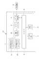
図1に示すように、画像読取装置2は、被写体を支持する支持台10と、この支持台10に支持された被写体を覆うカバー12とで構成されている。支持台10は、略長方形の板状に形成されている。カバー12は、略直方体の開口箱状に形成されている。支持台10には、有機CMOSイメージセンサ14が設けられている。有機CMOSイメージセンサ14は、支持台10の上面(支持面)10aに受光面14aを露呈させている。受光面14aは、縦10cm×横15cmの略長方形状に形成されている。なお、受光面14aの面積、及び形状は、当然、これに限定されるものではない。 As shown in FIG. 1, the
この画像読取装置2は、例えば、化学発光基質と接触して発光している被写体や蛍光色素で標識された被写体などを受光面14a上に直接乗せる。そして、有機CMOSイメージセンサ14を駆動して受光面14a全体を読み取ることにより、被写体の化学発光又は蛍光状態に応じた画像データを取得する。なお、被写体とは、例えば、タンパク質、酵素、核酸、DNA、RNAなどといった生体由来物質を含む溶液やゲル支持体、及びこれらの生体由来物質が転写されたメンブレンフイルムなどである。さらに、被写体は、例えば、発光試薬や蛍光試薬などが投与されたマウスやラットなどの動物(いわゆる、インビボイメージングを行うもの)であってもよい。 The
カバー12は、開口側が上面10aと向き合うように、ヒンジ部15を介して支持台10に回動自在に取り付けられている。これにより、カバー12は、受光面14aを露呈させた開き位置(図1参照)と、受光面14aを覆う閉じ位置(図2参照)との間で移動する。閉じ位置に移動したカバー12は、受光面14aを覆って遮光することにより、画像読み取りの際に、被写体が発する化学発光や蛍光以外の光が有機CMOSイメージセンサ14に入射することを防ぐ。 The
カバー12の内底面12aには、紫外線を照射する複数本の紫外線蛍光管(光源)16が設けられている。各紫外線蛍光管16は、カバー12が閉じ位置に移動した際に、受光面14aと対面し、受光面14aに向けて400nm以下の波長の紫外線を照射する。また、各紫外線蛍光管16は、受光面14aの全域に亘って均一な光量の紫外線が照射されるように、等間隔に並べて配置されている。これらの各紫外線蛍光管16は、蛍光標識された被写体を励起させるための励起光源である。画像読取装置2は、蛍光標識された被写体が受光面14a上に乗せられた際に、各紫外線蛍光管16を点灯させて被写体に紫外線を照射し、蛍光標識された被写体を励起させる。なお、励起光の波長は、上記に限ることなく、被写体の励起が可能な任意の波長でよい。 On the
支持台10の上面10aには、受光面14aを囲むように枠状に形成されたシール部材17が設けられている。一方、閉じ位置に移動した際に支持台10の上面10aと接触するカバー12の開口端面12bには、シール部材17に対応して枠状に形成された溝18が形成されている。シール部材17は、シリンドリカル状に突出して形成されている。そして、シール部材17は、カバー12が閉じ位置に移動した際に、溝18内に入り込み、溝18の底面と接触して押し潰されるように弾性変形する。シール部材17は、このように弾性変形することにより、カバー12による遮光性を高める。 A
また、マウスやラットなどの動物を被写体として撮影する場合には、これらの動物が動かないように、カバー12を閉じ位置にした際に生じる内部空間に、催眠ガスや麻酔ガスなどが注入される。シール部材17は、弾性変形することにより、前記内部空間の気密性を高め、催眠ガスや麻酔ガスなどが外部に漏れることを防止する。なお、シール部材17には、例えば、シリコーンゴムなどの樹脂材料を用いればよい。また、シール部材17は、遮光性を高めるため、黒色などの透光性のないものを用いることが好ましい。さらに、シール部材17は、カバー12側に設けられていてもよい。また、支持台10とカバー12との少なくとも一方には、催眠ガスや麻酔ガスなどを注入するための注入口や、これらのガスの注入を制御するためのバルブなどが設けられていることが好ましい。 Also, when photographing animals such as mice and rats as subjects, hypnotic gas, anesthetic gas, and the like are injected into the internal space generated when the
図2に示すように、支持台10の内部には、空洞部20が形成されている。この空洞部20は、受光面14aと平行な面が、受光面14aよりも広い面積を有するように形成されている。空洞部20の天井面20aには、複数のペルチエ素子22と温度センサ24とが設けられている。各ペルチエ素子22と各温度センサ24とは、天井面20aにアレイ状に配置されている。また、各ペルチエ素子22は、例えば、前後左右に配置されたもの同士で冷却面と加熱面とが交互になるように配置されている。画像読取装置2は、各温度センサ24で温度をモニタしながら各ペルチエ素子22を制御することにより、有機CMOSイメージセンサ14を所定の温度に調節する。 As shown in FIG. 2, a
なお、各温度センサ24は、例えば、熱電対や測温抵抗体、及びサーミスタなど、温度を測定できるものであれば、如何なるものでもよい。また、有機CMOSイメージセンサ14の温度は、受光面14aに乗せられる被写体の種類などに応じて調節されることが好ましい。例えば、人間に関連する生体由来物質を含む被写体が受光面14a上に乗せられた場合などには、その生体由来物質の活動しやすい35〜37℃(体温と同程度の温度)に調節することが好適である。 Each
なお、有機CMOSイメージセンサ14を35〜37℃に調節すると、暗電流の増加などにともなう画質の劣化が懸念されるが、被写体を受光面14aに直接接触させることによって、露光時間を短くすることができるので、前述の温度に調節したとしても暗電流などの影響をあまり受けることはない。 When the organic
図3は、画像読取装置2の電気的構成を概略的に示すブロック図である。支持台10には、有機CMOSイメージセンサ14、ペルチエ素子22、温度センサ24の他に、支持台10の各部を統括的に制御するコントローラ30と、有機CMOSイメージセンサ14が取得したアナログの画像データをデジタルの画像データに変換するA/Dコンバータ32と、外部機器36とのデータの送受信を行うデータ転送部34とが設けられている。 FIG. 3 is a block diagram schematically showing the electrical configuration of the
コントローラ30は、有機CMOSイメージセンサ14に接続されている。コントローラ30は、有機CMOSイメージセンサ14に駆動信号を送信することによって、有機CMOSイメージセンサ14による画像読み取りを制御する。また、コントローラ30には、各ペルチエ素子22と各温度センサ24とが接続されている。コントローラ30は、各温度センサ24の出力をモニタし、その出力結果(すなわち、各温度センサ24の測定点の温度)に応じて各ペルチエ素子22に印加する電圧を変化させることにより、受光面14aの全域に亘って均一な温度になるように有機CMOSイメージセンサ14の温度を調節する。このように有機CMOSイメージセンサ14の温度を調節することにより、温度ムラによるシェーディングの発生を抑えることができる。 The
さらに、コントローラ30には、カバー12に設けられた各紫外線蛍光管16が接続されている。各紫外線蛍光管16の点灯/消灯は、コントローラ30によって切り替えられる。コントローラ30は、蛍光標識された被写体を撮影する際などに、前述のように各紫外線蛍光管16を点灯させる。なお、支持台10とカバー12との間の電気的な接続は、例えば、ヒンジ部15を介して支持台10とカバー12とに挿通されるフレキシブルプリント配線基板などによって行えばよい。 Further, each
A/Dコンバータ32は、有機CMOSイメージセンサ14から出力されるアナログの画像データを受信し、受信したアナログの画像データをデジタルの画像データに変換する。そして、A/Dコンバータ32は、変換したデジタルの画像データをデータ転送部34に送信する。 The A /
画像読取装置2は、データ転送部34を介して、例えば、パーソナルコンピュータなどといった外部機器36と接続される。データ転送部34は、A/Dコンバータ32から受信した画像データを外部機器36に転送するとともに、外部機器36から送信される制御信号などをコントローラ30に入力する。なお、支持台10にハードディスクドライブなどの記録手段を設け、取得した画像データを画像読取装置2内で一時的保管できるようにしてもよい。 The
図4は、有機CMOSイメージセンサ14の1画素を拡大して示す部分断面図である。有機CMOSイメージセンサ14は、CMOS構造が形成されたシリコン基板40と、このシリコン基板40の上に積層された光電変換部42と、この光電変換部42の上に積層されたフィルタ44と、このフィルタ44の上に積層されたセルフォックレンズアレイ(登録商標)46とを備えている。なお、有機CMOSイメージセンサ14の1画素のサイズは、例えば、2〜50μmであり、より好ましくは2〜20μmである。 FIG. 4 is an enlarged partial cross-sectional view showing one pixel of the organic
光電変換部42は、近赤外線の光を感知する近赤外線感光光電変換膜(以下、NIR光電変換膜と称す)50と、赤色の光を感知する赤色感光光電変換膜(以下、R光電変換膜と称す)51と、緑色の光を感知する緑色感光光電変換膜(以下、G光電変換膜と称す)52と、青色の光を感知する青色感光光電変換膜(以下、B光電変換膜と称す)53との4層の有機光電変換膜を有している。各光電変換膜50、51、52、53は、有機CMOSイメージセンサ14に光が入射した際に、対応する波長の光の光量に応じた電荷を発生させる。 The
また、各光電変換膜50、51、52、53は、NIR光電変換膜50、R光電変換膜51、G光電変換膜52、B光電変換膜53の順に積層されており、短い波長の光ほど先に感知されるようになっている。なお、NIR光電変換膜50は、例えば、700〜2500nmの波長の光を近赤外線として感知し、R光電変換膜51は、例えば、600〜700nmの波長の光を赤色として感知し、G光電変換膜52は、例えば、500〜600nmの波長の光を緑色として感知し、B光電変換膜53は、例えば、400〜500nmの波長の光を青色として感知する。また、各光電変換膜50、51、52、53は、対応する波長域でのピーク波長の吸収率が50%以上であることが好ましい。 Each
なお、各光電変換膜50、51、52、53は、例えば、ペリレン、テトラセン、ペンタセン、ピレン、に代表されるアセン類、およびその誘導体、ポリアセチレン誘導体、チオフェン環を有するポリチオフェン誘導体、ポリ( 3 − アルキルチオフェン) 誘導体、ポリ( 3 , 4 − エチレンジオキシチオフェン) 誘導体、ポリチエニレンビニレン誘導体、ベンゼン環を有するポリフェニレン誘導体、ポリフェニレンビニレン誘導体、窒素原子を有するポリピリジン誘導体、ポリピロール誘導体、ポリアニリン誘導体、ポリキノリン誘導体等の共役高分子化合物、ジメチルセクシチオフェン、クオータチオフェンに代表されるオリゴマー、銅フタロシアニン誘導体に代表される有機分子、トリフェニレン誘導体に代表されるディスコチック液晶、フェニルナフタレン誘導体、ベンゾチアゾール誘導体に代表されるスメクチック液晶、ポリ( 9 ,9 − ジアルキルフルオレン− ビチオフェン) 共重合体に代表される液晶ポリマー、銅フタロシアニン誘導体、亜鉛フタロシアニン誘導体、ポリチオフェン誘導体、ポリパラフェニレン誘導体、メロシアニン色素などといった有機化合物によって構成される。 The
また、各光電変換膜50、51、52、53には、一般的な色素や顔料を含有させることができ、例えば、ローダミンB 、エオシン− Y 、クマリンなどの色素材料や、アゾ顔料やスクアリリウム顔料、アズレニウム顔料、フタロシアニン顔料などを適用することができる。さらに、電気伝導度を調整するために、各光電変換膜50、51、52、53に適当なドーパントを含有してもよい。ドーパントの種類としては、アクセプター性のI2、Br2、Cl2、ICl、BF3、PF5、H2SO4、FeCl3、TCNQ(テトラシアノキノジメタン)、ドナー性のLi、K、Na、Eu、界面活性剤であるアルキルスルホン酸塩、アルキルベンゼンスルホン酸塩などを挙げることができる。Each
有機CMOSイメージセンサ14は、上述のように各光電変換膜50、51、52、53でNIR、R、G、Bの各波長の光を感知し、各光電変換膜50、51、52、53でNIR、R、G、Bの各波長の画像を個別に取得することにより、フルカラーの画像データ、及び近赤外の画像データを取得する。このように、有機CMOSイメージセンサ14は、画素毎にNIR、R、G、Bの各波長の光を感知するので、色フィルタなどを介して特定波長の光だけを各画素に感知させるイメージセンサなどと比べて高感度な撮影を行うことができる。 The organic
NIR光電変換膜50には、下面に接する電極膜54と、上面に接する電極膜55とが設けられている。下面側の電極膜54とシリコン基板40との間には、これらを絶縁する絶縁膜56が設けられている。また、下面側の電極膜54は、絶縁膜56を貫通するように形成された柱状のビア57を介してシリコン基板40に接続されている。 The NIR
R光電変換膜51には、下面に接する電極膜58と、上面に接する電極膜59とが設けられている。下面側の電極膜58とNIR光電変換膜50の上面側の電極膜55との間には、これらを絶縁する絶縁膜60が設けられている。また、下面側の電極膜58は、NIR光電変換膜50と各電極膜54、55と各絶縁膜56、60とを貫通するように形成された柱状のビア61を介してシリコン基板40に接続されている。 The R
G光電変換膜52には、下面に接する電極膜62と、上面に接する電極膜63とが設けられている。下面側の電極膜62とR光電変換膜51の上面側の電極膜59との間には、これらを絶縁する絶縁膜64が設けられている。また、下面側の電極膜62は、NIR光電変換膜50とR光電変換膜51と各電極膜54、54、58、59と各絶縁膜56、60、64とを貫通するように形成された柱状のビア65を介してシリコン基板40に接続されている。 The G
B光電変換膜53には、下面に接する電極膜66と、上面に接する電極膜67とが設けられている。下面側の電極膜66とG光電変換膜52の上面側の電極膜63との間には、これらを絶縁する絶縁膜68が設けられている。また、下面側の電極膜66は、NIR光電変換膜50とR光電変換膜51とG光電変換膜52と各電極膜54、55、58、59、62、63と各絶縁膜56、60、64、68とを貫通するように形成された柱状のビア69を介してシリコン基板40に接続されている。 The B
なお、NIR光電変換膜50の下面側の電極膜54を除く各電極膜55、58、59、62、63、66、67は、透光性を有する透明電極になっている。このような透明電極には、例えば、ITO(Indium Tin Oxide)、IZO(Indium Zinc Oxide)、ZnO(酸化亜鉛)、SnO2(酸化錫)などが用いられる。In addition, each
また、NIR光電変換膜50の下に形成された絶縁膜56を除く各絶縁膜60、64、68は、透光性を有する透明絶縁膜になっている。このような透明絶縁膜には、例えば、窒化珪素、酸化珪素、ガラス、ポリエチレン、ポリエチレンテレフタレート、ポリエーテルサルフォン、ポリプロピレンなどが用いられる。特に、プラズマCVDで製膜される窒化珪素は、緻密性が高く、透明性もよいため、好適である。 Further, the insulating
シリコン基板40の各ビア57、61、65、69と接する部分には、各光電変換膜50、51、52、53のそれぞれに対応した電荷蓄積領域70、71、72、73が形成されている。NIR光電変換膜50に生じた電荷は、対応する各電極膜54、55に電圧を印加することにより、ビア57を介して電荷蓄積領域70に送られる。また、R光電変換膜51に生じた電荷は、対応する各電極膜58、59に電圧を印加することにより、ビア61を介して電荷蓄積領域71に送られる。また、G光電変換膜52に生じた電荷は、対応する各電極膜62、63に電圧を印加することにより、ビア65を介して電荷蓄積領域72に送られる。さらに、B光電変換膜53に生じた電荷は、対応する各電極膜66、67に電圧を印加することにより、ビア69を介して電荷蓄積領域73に送られる。また、シリコン基板40には、周知の転送回路(図示は省略)が形成されている。各電荷蓄積領域70、71、72、73に蓄積された電荷は、転送回路によって転送され、アナログの画像データとして出力される。
フィルタ44は、各紫外線蛍光管16の照射する紫外線の波長域のみをカットする帯域除去フィルタになっている。フィルタ44は、画像読み取りの際に、被写体が放出する化学発光又は蛍光のみを透過させ、励起光である紫外線が光電変換部42に入射することを防止する。これにより、紫外線に起因するバックグラウンドノイズを防止して、被写体の化学発光又は蛍光の検出感度を向上させることができる。 The
セルフォックレンズアレイ46は、画素毎に並べられた複数のロッドレンズを有している。このセルフォックレンズアレイ46は、入射してくる光を光電変換部42に案内するとともに、光電変換部42などを保護する保護膜として機能する。以上、有機CMOSイメージセンサ14の構成について説明したが、有機CMOSイメージセンサ14の構成は、例えば、特開2007−12796号公報などに、より詳細に説明されている。 The
次に、図5に示すフローチャートを参照しながら、蛍光標識された被写体を撮影する場合を例に、上記構成による画像読取装置2の作用について説明する。画像読取装置2で被写体の画像を取得する際には、例えば、電源スイッチ(図示は省略)をONするなどして、画像読取装置2の電源を入れる。画像読取装置2のコントローラ30は、電源が入れられたことに応じて各ペルチエ素子22と各温度センサ24とによる有機CMOSイメージセンサ14の温度調節を開始する。 Next, the operation of the
このように有機CMOSイメージセンサ14の温度を調節することで、温度ムラによるシェーディングの発生を抑えることができる。また、これに接触する被写体の温度をも調節し、被写体に含まれる生体由来物質を活性化させることなどもできる。さらに、電源のONなどと同時に予め有機CMOSイメージセンサ14の温度を調節しておくことで、例えば、被写体となる動物を眠らせた状態で受光面14aの上に乗せる際などに、睡眠により低下しがちな動物の体温を保持することができる。 By adjusting the temperature of the organic
画像読取装置2の電源を入れたら、カバー12を開き位置(図1参照)に移動させて、有機CMOSイメージセンサ14の受光面14aを露呈させる。受光面14aを露呈させたら、予め容易された被写体を受光面14aの上に乗せ、被写体を受光面14aに直接接触させる。被写体を受光面14a上に乗せたら、ヒンジ部15を軸にカバー12を回動させ、開き位置にあるカバー12を閉じ位置(図2参照)に移動させる。閉じ位置に移動したカバー12は、受光面14a、及びその上に乗せられた被写体を覆って遮光する。また、この際、支持台10の上面10aに設けられたシール部材17が溝18の底面と接触して弾性変形し、カバー12によって形成される内部空間の遮光性と気密性とを高める。 When the
カバー12を閉じ位置に移動させたら、例えば、データ転送部34を介して接続される外部機器36などから画像読取装置2に画像読み取りの開始指示を送信する。画像読取装置2に送信された開始指示は、データ転送部34を介してコントローラ30に入力される。なお、画像読み取りの開始指示は、これに限ることなく、例えば、支持台10に開始ボタンを設け、開始ボタンの押圧操作などに応じて開始指示が入力されるようにしてもよい。 When the
開始指示を受け取ったコントローラ30は、各紫外線蛍光管16を点灯させ、被写体に紫外線を照射する。蛍光標識された被写体は、励起光である紫外線を受けることによって励起し、生体由来物質などの反応状況に応じた光量の蛍光を放出する。各紫外線蛍光管16を点灯させたコントローラ30は、例えば、点灯から所定の時間が経過したか否かを判定し、所定時間の経過とともに各紫外線蛍光管16を消灯させる。 Receiving the start instruction, the
各紫外線蛍光管16を消灯させたコントローラ30は、有機CMOSイメージセンサ14に駆動信号を送信する。駆動信号を受信した有機CMOSイメージセンサ14は、その駆動信号に応じて撮影を行い、アナログの画像データを取得する。この際、有機CMOSイメージセンサ14は、NIR光電変換膜50、R光電変換膜51、G光電変換膜52、B光電変換膜53の4層の光電変換膜を有しているので、被写体の蛍光色に応じたカラーの画像データ、及び近赤外の画像データを取得することができる。 The
取得されたアナログの画像データは、A/Dコンバータ32に送られ、デジタルの画像データに変換される。変換された画像データは、データ転送部34に送られ、データ転送部34を介して外部機器36に転送される。以上により、被写体の蛍光に応じた画像が取得され、この画像を基に被写体に含まれる生体由来物質の分析などが行われる。 The acquired analog image data is sent to the A /
このように、本実施形態の画像読取装置2によれば、被写体を有機CMOSイメージセンサ14の受光面14aに直接接触させて撮影を行うようにしたので、光学系による光の減衰などがない高感度な撮影を行うことができる。また、化学発光や蛍光の検出感度が向上したことにより、有機CMOSイメージセンサ14の露出を短時間で行うことができる。さらに、被写体を受光面14aに直接接触させるようにしたことにより、光学系の結像などにともなう鉛直方向の余分なスペースが必要なくなるので、画像読取装置2の薄型化を実現することができる。 As described above, according to the
なお、上記実施形態では、カバー12の内面に複数本の紫外線蛍光管16を設けることによって、受光面14aの全域に均一な光量の紫外線が照射されるようにしているが、これに限ることなく、例えば、図6に示す画像読取装置75のように構成してもよい。図6の画像読取装置75は、1本の紫外線蛍光管76と、この紫外線蛍光管76をスライド移動させる蛍光管移動機構(光源移動手段)77とを備えている。なお、上記実施形態と機能・構成上同一のものについては、同符号を付し、詳細な説明を省略する。 In the above embodiment, a plurality of
紫外線蛍光管76は、カバー12の内底面に設けられている。また、紫外線蛍光管76は、例えば、カバー12に形成されたレール(図示は省略)に両端部を支持されることなどによって、カバー12の横方向にスライド自在に取り付けられる。蛍光管移動機構77は、コントローラ30に接続されており、コントローラ30からの制御信号に応じて紫外線蛍光管76を一定速度でスライド移動させる。 The
カバー12を閉じ位置にした状態で蛍光管移動機構77駆動すると、紫外線蛍光管76が受光面14aに対して平行に移動する。これにより、カバー12を閉じ位置にした状態で紫外線蛍光管76を点灯させ、蛍光管移動機構77駆動して紫外線蛍光管76を一定速度でスライド移動させることで、上記実施形態と同様に、受光面14aの全域に均一な光量の紫外線を照射することができる。なお、蛍光管移動機構77には、例えば、ラックアンドピニオンやボールネジなどによる周知の機構を用いればよい。 When the fluorescent
また、上記実施形態では、各紫外線蛍光管16を光源として備えることにより、蛍光標識された被写体などの画像を取得するようにしているが、これに限ることなく、例えば、図7に示す画像読取装置80のように構成してもよい。図7の画像読取装置80は、上記第1の実施形態の各紫外線蛍光管16に替えて、複数本の白色蛍光管82を備えている。各白色蛍光管82は、各紫外線蛍光管16と同様に、カバー12の内面に設けられ、カバー12が閉じ位置に移動した際に、受光面14aと対面し、受光面14aに向けて白色光を照射する。また、各白色蛍光管82は、受光面14aの全域に亘って均一な光量の白色光が照射されるように、等間隔に並べて配置されている。 In the above embodiment, each
この画像読取装置80は、各白色蛍光管82から白色光を被写体に照射することにより、例えば、クマシーブリリアントブルー(CBB)染色液などによって染色された有色の被写体の画像読み取りを行う。画像読取装置80は、各白色蛍光管82から白色光を被写体に照射し、その透過光を有機CMOSイメージセンサ14で検出する。これにより、生体由来物質などの反応状況に応じた濃淡の画像が取得される。 The
次に、図8に示すフローチャートを参照しながら、有色の被写体の画像読み取りの手順について説明する。画像読取装置80のコントローラ30は、電源が入力されたことなどに応じて各ペルチエ素子22と各温度センサ24とによる有機CMOSイメージセンサ14の温度調節を開始する。そして、コントローラ30は、外部機器36などから入力される画像読み取りの開始指示を受けたことに応じて、各白色蛍光管82を点灯させる。各白色蛍光管82を点灯させたコントローラ30は、有機CMOSイメージセンサ14に駆動信号を送信する。駆動信号を受信した有機CMOSイメージセンサ14は、その駆動信号に応じて撮影を行い、白色光を検出してアナログの画像データを取得する。有機CMOSイメージセンサ14を駆動してアナログの画像データを取得したコントローラ30は、各白色蛍光管82を消灯させる。 Next, a procedure for reading an image of a colored subject will be described with reference to the flowchart shown in FIG. The
取得されたアナログの画像データは、A/Dコンバータ32に送られる。A/Dコンバータ32は、受信したアナログの画像データをデジタルの画像データに変換する。この際、A/Dコンバータ32は、変換したデジタルの画像データの各画素が飽和しているか否か(デジタル値が最大になっているか否か)を判定する。各白色蛍光管82からの白色光を有機CMOSイメージセンサ14で検出する場合、被写体が乗っていない場所や被写体中の染色されていない場所に対応する画素は、飽和してしまう。このような画素は、被写体に含まれる生体由来物質の分析などに必要とならない。 The acquired analog image data is sent to the A /
このため、A/Dコンバータ32は、画像データの各画素の出力値が飽和しているか否かを判定し、飽和していると判定した際には、その画素の出力値を、例えば、バックグラウンドレベル(光が入射していない状態で出力される値)に設定する。すなわち、このA/Dコンバータ32が請求項記載の画像処理手段に相当している。なお、A/Dコンバータ32が設定する飽和画素の出力値は、バックグラウンドレベルに限ることなく、最大値以下の任意の値でよい。 For this reason, the A /
A/D変換、及び飽和画素の判定などが行われた画像データは、データ転送部34に送られ、データ転送部34を介して外部機器36に転送される。このように、画像読取装置80は、白色蛍光管82を用いることによって、有色の被写体の画像を取得する。なお、図7では、白色光を照射する光源として白色蛍光管82を示したが、これに限ることなく、有色の被写体を照明できるものであれば、如何なるものであってもよい。 Image data that has undergone A / D conversion, saturation pixel determination, and the like is sent to the
また、画像読取装置80は、白色蛍光管82を点灯させずに撮影を行うことで、化学発光する被写体の画像も取得することができる。さらには、白色蛍光管82を点灯させた状態と消灯させた状態とで撮影を行うことにより、有色の部分と化学発光する部分とが混在した被写体の画像も取得することができる。なお、この場合には、1つの被写体に対して有色の部分の画像と化学発光する部分の画像とが取得されるので、これらの各画像を合成して1つの画像にまとめるようにしてもよい。 The
また、上記実施形態では、支持台10に有機CMOSイメージセンサ14を設けたが、これに限ることなく、図9に示す画像読取装置90のように構成してもよい。図9の画像読取装置90は、カバー12側に有機CMOSイメージセンサ92を備えている。有機CMOSイメージセンサ92は、カバー12の内面に受光面92aを露呈させている。 Moreover, in the said embodiment, although the organic
一方、画像読取装置90の支持台10には、複数の光源94と透光板96とが設けられている。各光源94は、支持台10の内部に等間隔に並べて設けられている。透光板96は、支持台10に乗せられる被写体を支持するとともに、支持台10の内部に設けられた各光源94の光が被写体に当たるように、各光源94の光を透過させる。なお、各光源94は、被写体に励起光を照射するものでもよいし、白色光を照射するものでもよい。また、透光板96は、透明なガラスや樹脂材料などでもよいし、透光性と光拡散性とを有する乳白色の樹脂材料などでもよい。 On the other hand, the
有機CMOSイメージセンサ92は、カバー12が閉じ位置に移動した際に、受光面92aを透光板96の表面に接触させる。この画像読取装置90は、被写体を透光板96の上に乗せた後、カバー12を閉じ位置に移動させて透光板96上の被写体と受光面92aとを接触させる。そして、有機CMOSイメージセンサ92を駆動して受光面92a全体を読み取ることにより、被写体の画像データを取得する。このように、カバー12側に有機CMOSイメージセンサ92を設けても、受光面92aを被写体に直接接触させて撮影を行うことができるので、上記実施形態と同様の効果を得ることができる。なお、図9では、透光板96を介して光源94の光を被写体に照射するようにしているが、これに限ることなく、例えば、有機ELなどのシート状の光源を用いて、光源の上に直接被写体を乗せるようにしてもよい。 The organic
さらには、図10に示す画像読取装置100のように、支持台10とカバー12との双方にイメージセンサを設けてもよい。図10の画像読取装置100は、支持台10に設けられた第1有機CMOSイメージセンサ102と、カバー12に設けられた第2有機CMOSイメージセンサ104とを備えている。第1有機CMOSイメージセンサ102は、支持台10の上面に受光面102aを露呈させている。一方、第2有機CMOSイメージセンサ104は、カバー12の内面に受光面104aを露呈させている。各有機CMOSイメージセンサ102、104は、カバー12が閉じ位置に移動した際に、各受光面102a、104aを互いに接触させる。 Furthermore, an image sensor may be provided on both the
この画像読取装置100は、被写体を第1有機CMOSイメージセンサ102の受光面102a上に直接乗せる。この後、カバー12を閉じ位置に移動させて、第1有機CMOSイメージセンサ102の受光面102a上の被写体と、第2有機CMOSイメージセンサ104の受光面104aとを接触させる。そして、各有機CMOSイメージセンサ102、104を駆動することにより、各有機CMOSイメージセンサ102、104のそれぞれで被写体の画像データを取得する。 The
また、図11に示すように、支持台10の内部には、各有機CMOSイメージセンサ102、104のそれぞれが取得した2つの画像データを1つの画像データに合成する画像合成部(画像合成手段)106が設けられている。画像合成部106は、各有機CMOSイメージセンサ102、104の対面する画素(すなわち、被写体の同じ部分を撮影した画素)の出力値を足し合わせることによって、2つの画像データを1つの画像データに合成する。 As shown in FIG. 11, an image composition unit (image composition means) for synthesizing two image data acquired by each of the organic
各有機CMOSイメージセンサ102、104が取得したアナログの画像データは、A/Dコンバータ32に入力される。A/Dコンバータ32は、入力された各画像データをデジタルの画像データに変換し、変換した各画像データを画像合成部106に送る。画像合成部106は、A/Dコンバータ32から各画像データを受け取ると、前述のように各画素の出力値を足し合わせることによって1つの画像データを作成し、作成した画像データをデータ転送部34に送る。これにより、各有機CMOSイメージセンサ102、104によって取得された画像データが、1つの画像データとして外部機器36に転送される。 Analog image data acquired by each of the organic
このように、支持台10とカバー12との双方に有機CMOSイメージセンサ102、104を設けても、各受光面102a、104aを被写体に直接接触させて撮影を行うことができるので、上記実施形態と同様の効果を得ることができる。さらに、被写体の表側と裏側とから撮影したそれぞれの画像データを合成することで、被写体の化学発光などの検出感度をより向上させることができる。 As described above, even if the organic
なお、図11では、A/Dコンバータ32の後段に画像合成部106を設け、A/Dコンバータ32によって変換されたデジタルの各画像データを合成するようにしているが、これに限ることなく、図12に示すように、A/Dコンバータ32の前段に画像合成部106を設け、各有機CMOSイメージセンサ102、104から出力されるアナログの各画像データを合成するようにしてもよい。 In FIG. 11, an
また、図10に示す構成では、励起光や白色光を照射する光源が設けられていないため、化学発光する被写体しか撮影することができない。このため、例えば、各有機CMOSイメージセンサ102、104を製造する際に、光電変換部42とともにLEDなどの発光部をシリコン基板40の上に形成し、各受光面102a、104aを発光させることによって、蛍光標識された被写体や有色の被写体などを撮影できるようにしてもよい。 Further, in the configuration shown in FIG. 10, since no light source that emits excitation light or white light is provided, only a subject that emits chemiluminescence can be photographed. For this reason, for example, when manufacturing each of the organic
なお、上記各実施形態では、イメージセンサとしてフルカラーの画像データ、及び近赤外の画像データを取得する4層構造の有機CMOSイメージセンサを示したが、イメージセンサは、これに限ることなく、例えば、3層構造、2層構造のものでもよいし、単層のモノクロ撮影のものでもよい。また、有機CMOSイメージセンサを3層構造とする場合には、R、G、Bの組み合わせにしてもよいし、NIR、R、Gの組み合わせにしてもよい。また、上記各実施形態では、CMOSタイプのイメージセンサを示したが、これに限ることなく、例えば、CCDタイプのイメージセンサとしてもよい。 In each of the above embodiments, the four-layer organic CMOS image sensor that acquires full-color image data and near-infrared image data is shown as the image sensor. However, the image sensor is not limited to this, and for example, A three-layer structure, a two-layer structure, or a single-layer monochrome image may be used. When the organic CMOS image sensor has a three-layer structure, it may be a combination of R, G, and B, or a combination of NIR, R, and G. In each of the above embodiments, a CMOS type image sensor is shown. However, the present invention is not limited to this, and for example, a CCD type image sensor may be used.
さらに、上記各実施形態では、有機光電変換膜を有する、いわゆる有機撮像素子をイメージセンサとして示したが、これに限ることなく、例えば、ベイヤー配列されたカラーフィルタなどを有する一般的な無機の撮像素子や有機と無機とが混在したハイブリット型の撮像素子などを用いてもよい。但し、無機の撮像素子は、半導体の製造プロセスの問題から大面積化が難しい。このため、縦10cm×横15cm程度の受光面を有するイメージセンサを用いる際には、上記各実施形態に示すように、有機撮像素子を用いることが好ましい。なお、前述のように、受光面の面積は、特に限定されるものではないが、縦10cm×横15cm以上の面積を有していると、例えば、96穴のマイクロタイタープレートを直接受光面に乗せ、各ウエルに試料溶液を入れた状態で撮影を行うことなどができ、画像読取装置の汎用性の向上などを図ることができる。 Further, in each of the above embodiments, a so-called organic imaging device having an organic photoelectric conversion film is shown as an image sensor. However, the present invention is not limited to this, and for example, a general inorganic imaging having a Bayer array color filter or the like. An element or a hybrid imaging element in which organic and inorganic are mixed may be used. However, it is difficult to increase the area of the inorganic imaging element due to the problem of the semiconductor manufacturing process. For this reason, when using an image sensor having a light receiving surface of about 10 cm in length × 15 cm in width, it is preferable to use an organic imaging device as shown in the above embodiments. As described above, the area of the light receiving surface is not particularly limited. However, if it has an area of 10 cm in length × 15 cm in width, for example, a 96-well microtiter plate is directly attached to the light receiving surface. An image can be taken with the sample solution placed in each well, and the versatility of the image reading apparatus can be improved.
なお、上記各実施形態では、保護膜としてセルフォックレンズアレイ46を示したが、保護膜は、これに限ることなく、例えば、マイクロキャピラリプレート、ダイヤモンド薄膜、金属酸化膜、金属窒化膜、フッ素樹脂、ポリパラキシレン、シリコーン樹脂、ポリスチレン樹脂、光硬化性樹脂などを用いることができる。 In each of the above embodiments, the
また、上記各実施形態では、回動自在に支持台10取り付けられたカバー12を示しているが、カバー12は、これに限ることなく、例えば、閉じ位置と開き位置との間でスライド移動するものでもよいし、支持台10に対して着脱自在なものでもよい。 Moreover, in each said embodiment, although the
さらに、上記各実施形態では、光源として、紫外線蛍光管16、76、及び白色蛍光管82などの円柱状の蛍光管を示したが、光源は、これに限ることなく、例えば、LEDやレーザダイオード、及びハロゲンランプと拡散板とを組み合わせたものなど、被写体の励起又は照明が可能な周知の光源を用いればよい。また、上記各実施形態では、複数のペルチエ素子22と温度センサ24とからなる温度調節手段を示したが、温度調節手段は、これに限ることなく、例えば、温度調節された液体や気体を循環させる熱交換器や、電熱ヒータを用いるものなどであってもよい。 Further, in each of the above embodiments, columnar fluorescent tubes such as the
2、75、80、90、100 画像読取装置
10 支持台
10a 上面(支持面)
12 カバー
14、92 有機CMOSイメージセンサ(イメージセンサ)
14a、92a 受光面
16、76 紫外線蛍光管(光源)
20 空洞部
20a 天井面
22 ペルチエ素子
24 温度センサ
32 A/Dコンバータ(画像処理手段)
44 フィルタ
46 セルフォックレンズアレイ(保護膜)
50 近赤外線感光光電変換膜(有機光電変換膜)
51 赤色感光光電変換膜(有機光電変換膜)
52 緑色感光光電変換膜(有機光電変換膜)
53 青色感光光電変換膜(有機光電変換膜)
77 蛍光管移動機構(光源移動手段)
82 白色蛍光管(光源)
94 光源
102 第1有機CMOSイメージセンサ
102a 受光面
104 第2有機CMOSイメージセンサ
104a 受光面
106 画像合成部(画像合成手段)2, 75, 80, 90, 100
12
14a, 92a
20
44
50 Near-infrared photosensitive photoelectric conversion film (organic photoelectric conversion film)
51 Red photosensitive photoelectric conversion film (organic photoelectric conversion film)
52 Green photosensitive photoelectric conversion film (organic photoelectric conversion film)
53 Blue photosensitive photoelectric conversion film (organic photoelectric conversion film)
77 Fluorescent tube moving mechanism (light source moving means)
82 White fluorescent tube (light source)
94
Claims (21)
Translated fromJapanese前記被写体を支持する支持面を有する支持台と、
前記支持面を覆って遮光するカバーと、
受光面から入射した光の光量に応じて電荷を発生させる有機光電変換膜を有し、前記受光面が前記支持面に露呈するように前記支持台に設けられ、前記受光面に前記被写体を乗せた状態で前記被写体の撮影を行うイメージセンサとを備えたことを特徴とする画像読取装置。In an image reading device that captures an image of a subject including a biological substance and obtains an image according to a reaction state of the biological substance,
A support base having a support surface for supporting the subject;
A cover for covering and shielding the support surface;
An organic photoelectric conversion film that generates an electric charge according to the amount of light incident from the light receiving surface; provided on the support base such that the light receiving surface is exposed to the support surface; and placing the subject on the light receiving surface. An image reading apparatus comprising: an image sensor that captures an image of the subject in a state where the image is captured.
前記イメージセンサは、前記被写体を透過した前記白色光を撮影することを特徴とする請求項2から4のいずれか1項に記載の画像読取装置。The light source irradiates the light receiving surface with white light,
5. The image reading apparatus according to claim 2, wherein the image sensor captures the white light transmitted through the subject.
前記イメージセンサは、前記励起によって生じる蛍光を撮影することを特徴とする請求項2から6のいずれか1項に記載の画像読取装置。The light source irradiates excitation light that excites the subject labeled with the biological substance by a fluorescent dye,
The image reading apparatus according to claim 2, wherein the image sensor photographs fluorescence generated by the excitation.
前記温度調節手段は、前記空洞部の天井面にアレイ状に配置される複数のペルチエ素子と温度センサとで構成されることを特徴とする請求項8記載の画像読取装置。A cavity is formed inside the support base,
9. The image reading apparatus according to claim 8, wherein the temperature adjusting means includes a plurality of Peltier elements and temperature sensors arranged in an array on the ceiling surface of the cavity.
前記被写体を支持する支持面を有する支持台と、
前記支持面を覆って遮光するカバーと、
受光面から入射した光の光量に応じて電荷を発生させる有機光電変換膜を有し、前記支持面を覆う閉じ位置に前記カバーがある際に、前記支持面上の前記被写体に前記受光面が接触するように前記カバーの内面に設けられ、前記受光面に前記被写体を接触させた状態で前記被写体の撮影を行うイメージセンサとを備えたことを特徴とする画像読取装置。In an image reading device that captures an image of a subject including a biological substance and obtains an image according to a reaction state of the biological substance,
A support base having a support surface for supporting the subject;
A cover for covering and shielding the support surface;
An organic photoelectric conversion film that generates an electric charge according to the amount of light incident from the light receiving surface, and when the cover is in a closed position that covers the support surface, the light receiving surface is placed on the subject on the support surface. An image reading apparatus, comprising: an image sensor that is provided on an inner surface of the cover so as to be in contact with the image sensor and photographs the subject in a state where the subject is in contact with the light receiving surface.
前記被写体を支持する支持面を有する支持台と、
前記支持面を覆って遮光するカバーと、
受光面から入射した光の光量に応じて電荷を発生させる有機光電変換膜を有し、前記受光面が前記支持面に露呈するように前記支持台に設けられ、前記受光面に前記被写体を乗せた状態で前記被写体の撮影を行う第1イメージセンサと、
受光面から入射した光の光量に応じて電荷を発生させる有機光電変換膜を有し、前記支持面を覆う閉じ位置に前記カバーがある際に、前記支持面上の前記被写体に前記受光面が接触するように前記カバーの内面に設けられ、前記受光面に前記被写体を接触させた状態で前記被写体の撮影を行う第2イメージセンサとを備えたことを特徴とする画像読取装置。In an image reading device that captures an image of a subject including a biological substance and obtains an image according to a reaction state of the biological substance,
A support base having a support surface for supporting the subject;
A cover for covering and shielding the support surface;
An organic photoelectric conversion film that generates an electric charge according to the amount of light incident from the light receiving surface; provided on the support base such that the light receiving surface is exposed to the support surface; and placing the subject on the light receiving surface. A first image sensor for taking a picture of the subject in a closed state;
An organic photoelectric conversion film that generates an electric charge according to the amount of light incident from the light receiving surface, and when the cover is in a closed position that covers the support surface, the light receiving surface is placed on the subject on the support surface. An image reading apparatus, comprising: a second image sensor that is provided on an inner surface of the cover so as to come into contact, and that photographs the subject in a state where the subject is in contact with the light receiving surface.
前記A/Dコンバータが変換したデジタルの各画像データを合成して1つの合成画像データを作成する画像合成手段とを設けたことを特徴とする請求項16記載の画像読取装置。An A / D converter that converts each of the analog first image data acquired by the first image sensor and the analog second image data acquired by the second image sensor into digital image data;
17. The image reading apparatus according to claim 16, further comprising an image synthesizing unit that synthesizes digital image data converted by the A / D converter to create one synthesized image data.
前記画像合成手段が作成したアナログの前記合成画像データをデジタルの画像データに変換するA/Dコンバータとを設けたことを特徴とする請求項16記載の画像読取装置。Image synthesizing means for synthesizing the analog first image data acquired by the first image sensor and the analog second image data acquired by the second image sensor to create one synthesized image data;
17. The image reading apparatus according to claim 16, further comprising an A / D converter that converts the analog synthesized image data created by the image synthesizing unit into digital image data.
前記受光面を前記被写体に直接接触させた状態で撮影を行うことを特徴とする画像読取方法。A support base having a support surface that supports a subject including a biological substance; a cover that covers and shields the support surface; and an organic photoelectric conversion film that generates an electric charge according to the amount of light incident from the light receiving surface An image sensor provided on at least one of the support base and the cover, and capturing an image corresponding to a reaction state of the biological substance contained in the subject by photographing the subject with the image sensor. In the image reading method of the reading device,
An image reading method, wherein photographing is performed with the light receiving surface in direct contact with the subject.
Priority Applications (2)
| Application Number | Priority Date | Filing Date | Title |
|---|---|---|---|
| JP2007082090AJP2008241447A (en) | 2007-03-27 | 2007-03-27 | Image reading apparatus and image reading method |
| US12/049,018US7773223B2 (en) | 2007-03-27 | 2008-03-14 | Image scanning apparatus and image scanning method |
Applications Claiming Priority (1)
| Application Number | Priority Date | Filing Date | Title |
|---|---|---|---|
| JP2007082090AJP2008241447A (en) | 2007-03-27 | 2007-03-27 | Image reading apparatus and image reading method |
Publications (1)
| Publication Number | Publication Date |
|---|---|
| JP2008241447Atrue JP2008241447A (en) | 2008-10-09 |
Family
ID=39794587
Family Applications (1)
| Application Number | Title | Priority Date | Filing Date |
|---|---|---|---|
| JP2007082090APendingJP2008241447A (en) | 2007-03-27 | 2007-03-27 | Image reading apparatus and image reading method |
Country Status (2)
| Country | Link |
|---|---|
| US (1) | US7773223B2 (en) |
| JP (1) | JP2008241447A (en) |
Cited By (7)
| Publication number | Priority date | Publication date | Assignee | Title |
|---|---|---|---|---|
| JP2011022087A (en)* | 2009-07-17 | 2011-02-03 | Shimadzu Corp | Living body image acquisition device |
| JP2013124877A (en)* | 2011-12-13 | 2013-06-24 | Hamamatsu Photonics Kk | Optical measurement device |
| WO2016007353A1 (en)* | 2014-07-07 | 2016-01-14 | Bio-Rad Laboratories, Inc. | Contact imager |
| KR20180006704A (en)* | 2016-07-11 | 2018-01-19 | 삼성전자주식회사 | Image sensor and electronic device including the same |
| KR20180027538A (en)* | 2015-07-08 | 2018-03-14 | 상하이 이-블롯 포토일렉트릭 테크놀로지 컴퍼니 리미티드 | Method and apparatus for signal acquisition of photosensitive chip and method and apparatus for cell tracking |
| WO2019069893A1 (en)* | 2017-10-05 | 2019-04-11 | パナソニックIpマネジメント株式会社 | Biomolecule detection method |
| JPWO2021182175A1 (en)* | 2020-03-11 | 2021-09-16 |
Families Citing this family (14)
| Publication number | Priority date | Publication date | Assignee | Title |
|---|---|---|---|---|
| JP5353200B2 (en)* | 2008-11-20 | 2013-11-27 | ソニー株式会社 | Solid-state imaging device and imaging device |
| EP3340610B1 (en)* | 2010-09-20 | 2022-11-16 | Fraunhofer-Gesellschaft zur Förderung der angewandten Forschung e.V. | Method for differentiating background and foreground of a setting and method for replacing a background in images of a setting |
| JP5349521B2 (en)* | 2011-03-29 | 2013-11-20 | 富士フイルム株式会社 | Imaging apparatus, imaging program, and imaging method |
| JP5759924B2 (en)* | 2011-06-06 | 2015-08-05 | 富士フイルム株式会社 | Color filter, CCD sensor, CMOS sensor, organic CMOS sensor, and solid-state imaging device |
| CN104115478B (en) | 2011-12-16 | 2016-04-20 | 利-考股份有限公司 | luminescence imaging scanner |
| USD721704S1 (en)* | 2013-06-06 | 2015-01-27 | Li-Cor, Inc. | Chemiluminescence compact imaging scanner lid |
| US20220260499A1 (en)* | 2015-07-08 | 2022-08-18 | Shanghai E-Blot Photoelectric Technology Co., Ltd | Method and apparatus for collecting signals, tracking cells, and imaging control using a photosensitive chip |
| WO2018058083A1 (en)* | 2016-09-26 | 2018-03-29 | Azure Biosystems, Inc. | Methods and devices for photometric analysis |
| JP6911430B2 (en)* | 2017-03-22 | 2021-07-28 | セイコーエプソン株式会社 | Image reader and semiconductor device |
| US12009379B2 (en)* | 2017-05-01 | 2024-06-11 | Visera Technologies Company Limited | Image sensor |
| CN119534433A (en) | 2017-12-15 | 2025-02-28 | 生物辐射实验室股份有限公司 | Combined imaging of assays |
| EP3867863A4 (en)* | 2018-10-15 | 2022-07-20 | Bio-Rad Laboratories, Inc. | Saturation avoidance in digital imaging |
| CN111751332B (en)* | 2019-03-28 | 2025-05-16 | 易孛特生命科学(上海)有限公司 | Imaging method and device for self-luminous objects on biological sample membrane |
| CN111751337A (en)* | 2019-03-28 | 2020-10-09 | 上海易孛特光电技术有限公司 | Fluorescence signal collection device and fluorescence signal collection system including the same |
Family Cites Families (4)
| Publication number | Priority date | Publication date | Assignee | Title |
|---|---|---|---|---|
| JPH06311879A (en)* | 1993-03-15 | 1994-11-08 | Nec Corp | Biosensor |
| CA2389358C (en)* | 1996-12-31 | 2008-07-15 | Genometrix Incorporated | Multiplexed molecular analysis apparatus and method |
| US6570158B2 (en)* | 2001-06-02 | 2003-05-27 | Hya Feygin | Method and apparatus for infrared-spectrum imaging |
| JP2005283322A (en) | 2004-03-30 | 2005-10-13 | Fuji Photo Film Co Ltd | Photographing device |
- 2007
- 2007-03-27JPJP2007082090Apatent/JP2008241447A/enactivePending
- 2008
- 2008-03-14USUS12/049,018patent/US7773223B2/ennot_activeExpired - Fee Related
Cited By (13)
| Publication number | Priority date | Publication date | Assignee | Title |
|---|---|---|---|---|
| JP2011022087A (en)* | 2009-07-17 | 2011-02-03 | Shimadzu Corp | Living body image acquisition device |
| JP2013124877A (en)* | 2011-12-13 | 2013-06-24 | Hamamatsu Photonics Kk | Optical measurement device |
| WO2016007353A1 (en)* | 2014-07-07 | 2016-01-14 | Bio-Rad Laboratories, Inc. | Contact imager |
| US9794454B2 (en) | 2014-07-07 | 2017-10-17 | Bio-Rad Laboratories, Inc. | Contact imager |
| JP2018524613A (en)* | 2015-07-08 | 2018-08-30 | シャンハイ イーブロット フォトエレクトリック テクノロジー カンパニー リミテッドShanghai E−Blot Photoelectric Technology Co., Ltd | Method and apparatus for signal collection by photosensitive chip, and method and apparatus for cell tracking |
| KR20180027538A (en)* | 2015-07-08 | 2018-03-14 | 상하이 이-블롯 포토일렉트릭 테크놀로지 컴퍼니 리미티드 | Method and apparatus for signal acquisition of photosensitive chip and method and apparatus for cell tracking |
| KR102084233B1 (en)* | 2015-07-08 | 2020-03-03 | 상하이 이-블롯 포토일렉트릭 테크놀로지 컴퍼니 리미티드 | Signal acquisition method and device of photosensitive chip and cell tracking method and device |
| JP2020115149A (en)* | 2015-07-08 | 2020-07-30 | シャンハイ イーブロット フォトエレクトリック テクノロジー カンパニー リミテッドShanghai E−Blot Photoelectric Technology Co., Ltd | Method and device for signal collection by photosensitive chip, and method and device for cell tracking |
| JP2022140791A (en)* | 2015-07-08 | 2022-09-27 | シャンハイ イーブロット フォトエレクトリック テクノロジー カンパニー リミテッド | Method and device for collecting signal using photosensitive chip, and method and device for tracking cell |
| KR20180006704A (en)* | 2016-07-11 | 2018-01-19 | 삼성전자주식회사 | Image sensor and electronic device including the same |
| KR102582122B1 (en)* | 2016-07-11 | 2023-09-21 | 삼성전자주식회사 | Image sensor and electronic device including the same |
| WO2019069893A1 (en)* | 2017-10-05 | 2019-04-11 | パナソニックIpマネジメント株式会社 | Biomolecule detection method |
| JPWO2021182175A1 (en)* | 2020-03-11 | 2021-09-16 |
Also Published As
| Publication number | Publication date |
|---|---|
| US20080240747A1 (en) | 2008-10-02 |
| US7773223B2 (en) | 2010-08-10 |
Similar Documents
| Publication | Publication Date | Title |
|---|---|---|
| JP2008241447A (en) | Image reading apparatus and image reading method | |
| US9412909B2 (en) | Light emitting apparatus, manufacturing method of light emitting apparatus, light receiving and emitting apparatus, and electronic equipment | |
| US20240305895A1 (en) | Imaging device and camera system | |
| dos Santos et al. | Investigation of the mechanisms giving rise to TADF in exciplex states | |
| US6596483B1 (en) | System and method for detecting molecules using an active pixel sensor | |
| Okada et al. | Photochromism and Thermally and Optically Stimulated Luminescences of AlN Ceramic Plate for UV Sensing. | |
| KR20190028661A (en) | A solid-state imaging device and a solid-state imaging device | |
| US9891192B2 (en) | System and method for flat panel detector gel and blot imaging | |
| Marcello et al. | A deep-blue OLED-based biochip for protein microarray fluorescence detection | |
| JP2015505046A (en) | Luminescence imaging scanner | |
| JP2000180361A (en) | Photographing system | |
| Liu et al. | Multiple approaches for enhancing all-organic electronics photoluminescent sensors: Simultaneous oxygen and pH monitoring | |
| US20120179383A1 (en) | Disc and calibration method of test device using the same | |
| CN105684149A (en) | Solid-state imaging device and electronic apparatus | |
| Kirch et al. | Accurate wavelength tracking by exciton spin mixing | |
| US20100091273A1 (en) | Reference Light Source Device | |
| Liang et al. | Color measurement for RGB white LEDs in solid-state lighting using a BDJ photodetector | |
| EP3350577B1 (en) | System and method for flat panel detector gel and blot imaging | |
| Balsam et al. | Smartphone-based fluorescence detector for mHealth | |
| Cumpson et al. | Multispectral optical imaging combined in situ with XPS or ToFSIMS and principal component analysis | |
| Lin et al. | Blue organic long-persistent luminescence via upconversion from charge-transfer to locally excited singlet state | |
| JP2010122087A (en) | Spectroscopic imaging apparatus | |
| Sen et al. | A new macro-imager based on Tpx3Cam optical camera for PLIM applications | |
| Yemini et al. | Illumination for worm tracking and behavioral imaging | |
| Vasilopoulou et al. | Photopatterned PLED arrays for biosensing applications |