JP2008235804A - Light emitting element - Google Patents
Light emitting elementDownload PDFInfo
- Publication number
- JP2008235804A JP2008235804AJP2007077037AJP2007077037AJP2008235804AJP 2008235804 AJP2008235804 AJP 2008235804AJP 2007077037 AJP2007077037 AJP 2007077037AJP 2007077037 AJP2007077037 AJP 2007077037AJP 2008235804 AJP2008235804 AJP 2008235804A
- Authority
- JP
- Japan
- Prior art keywords
- light
- layer
- nitride semiconductor
- group iii
- quantum well
- Prior art date
- Legal status (The legal status is an assumption and is not a legal conclusion. Google has not performed a legal analysis and makes no representation as to the accuracy of the status listed.)
- Pending
Links
Images


Classifications
- H—ELECTRICITY
- H10—SEMICONDUCTOR DEVICES; ELECTRIC SOLID-STATE DEVICES NOT OTHERWISE PROVIDED FOR
- H10H—INORGANIC LIGHT-EMITTING SEMICONDUCTOR DEVICES HAVING POTENTIAL BARRIERS
- H10H20/00—Individual inorganic light-emitting semiconductor devices having potential barriers, e.g. light-emitting diodes [LED]
- H10H20/80—Constructional details
- H10H20/81—Bodies
- H10H20/813—Bodies having a plurality of light-emitting regions, e.g. multi-junction LEDs or light-emitting devices having photoluminescent regions within the bodies
- H—ELECTRICITY
- H10—SEMICONDUCTOR DEVICES; ELECTRIC SOLID-STATE DEVICES NOT OTHERWISE PROVIDED FOR
- H10H—INORGANIC LIGHT-EMITTING SEMICONDUCTOR DEVICES HAVING POTENTIAL BARRIERS
- H10H20/00—Individual inorganic light-emitting semiconductor devices having potential barriers, e.g. light-emitting diodes [LED]
- H10H20/80—Constructional details
- H10H20/81—Bodies
- H10H20/817—Bodies characterised by the crystal structures or orientations, e.g. polycrystalline, amorphous or porous
- H—ELECTRICITY
- H01—ELECTRIC ELEMENTS
- H01L—SEMICONDUCTOR DEVICES NOT COVERED BY CLASS H10
- H01L2224/00—Indexing scheme for arrangements for connecting or disconnecting semiconductor or solid-state bodies and methods related thereto as covered by H01L24/00
- H01L2224/01—Means for bonding being attached to, or being formed on, the surface to be connected, e.g. chip-to-package, die-attach, "first-level" interconnects; Manufacturing methods related thereto
- H01L2224/10—Bump connectors; Manufacturing methods related thereto
- H01L2224/12—Structure, shape, material or disposition of the bump connectors prior to the connecting process
- H01L2224/14—Structure, shape, material or disposition of the bump connectors prior to the connecting process of a plurality of bump connectors
- H—ELECTRICITY
- H01—ELECTRIC ELEMENTS
- H01L—SEMICONDUCTOR DEVICES NOT COVERED BY CLASS H10
- H01L2224/00—Indexing scheme for arrangements for connecting or disconnecting semiconductor or solid-state bodies and methods related thereto as covered by H01L24/00
- H01L2224/01—Means for bonding being attached to, or being formed on, the surface to be connected, e.g. chip-to-package, die-attach, "first-level" interconnects; Manufacturing methods related thereto
- H01L2224/10—Bump connectors; Manufacturing methods related thereto
- H01L2224/15—Structure, shape, material or disposition of the bump connectors after the connecting process
- H01L2224/16—Structure, shape, material or disposition of the bump connectors after the connecting process of an individual bump connector
- H01L2224/161—Disposition
- H01L2224/16151—Disposition the bump connector connecting between a semiconductor or solid-state body and an item not being a semiconductor or solid-state body, e.g. chip-to-substrate, chip-to-passive
- H01L2224/16221—Disposition the bump connector connecting between a semiconductor or solid-state body and an item not being a semiconductor or solid-state body, e.g. chip-to-substrate, chip-to-passive the body and the item being stacked
- H01L2224/16225—Disposition the bump connector connecting between a semiconductor or solid-state body and an item not being a semiconductor or solid-state body, e.g. chip-to-substrate, chip-to-passive the body and the item being stacked the item being non-metallic, e.g. insulating substrate with or without metallisation
- H—ELECTRICITY
- H10—SEMICONDUCTOR DEVICES; ELECTRIC SOLID-STATE DEVICES NOT OTHERWISE PROVIDED FOR
- H10H—INORGANIC LIGHT-EMITTING SEMICONDUCTOR DEVICES HAVING POTENTIAL BARRIERS
- H10H20/00—Individual inorganic light-emitting semiconductor devices having potential barriers, e.g. light-emitting diodes [LED]
- H10H20/80—Constructional details
- H10H20/85—Packages
- H10H20/851—Wavelength conversion means
- H10H20/8511—Wavelength conversion means characterised by their material, e.g. binder
- H10H20/8512—Wavelength conversion materials
Landscapes
- Led Devices (AREA)
Abstract
Translated fromJapaneseDescription
Translated fromJapaneseこの発明は、窒化物半導体を用いて発光ダイオード構造を有する発光素子に関する。 The present invention relates to a light emitting element having a light emitting diode structure using a nitride semiconductor.
III-V族半導体においてV族元素として窒素を用いた半導体は「III族窒化物半導体」と呼ばれ、その代表例は、窒化アルミニウム(AlN)、窒化ガリウム(GaN)、窒化インジウム(InN)である。一般には、AlxInyGa1-x-yN(0≦x≦1,0≦y≦1,0≦x+y≦1)と表わすことができる。
c面を主面とする窒化ガリウム(GaN)基板上にIII族窒化物半導体を有機金属化学気相成長法(MOCVD法)によって成長させる窒化物半導体の製造方法が知られている。この方法を適用することにより、n型層およびp型層を有するGaN半導体積層構造を形成することができ、この積層構造を利用した発光デバイスを作製できる。このような発光デバイスは、たとえば、液晶パネル用バックライトの光源として利用可能である。
A nitride semiconductor manufacturing method is known in which a group III nitride semiconductor is grown on a gallium nitride (GaN) substrate having a c-plane as a main surface by metal organic chemical vapor deposition (MOCVD). By applying this method, a GaN semiconductor multilayer structure having an n-type layer and a p-type layer can be formed, and a light-emitting device using this multilayer structure can be manufactured. Such a light emitting device can be used as a light source of a backlight for a liquid crystal panel, for example.
III族窒化物半導体で500nm以上の長波長域の発光波長を持つ活性層を形成すると、このような活性層は、熱ダメージに弱いことが分かっている。具体的には、たとえば、GaN基板上にn型GaN半導体層を成長させ、これにIII族窒化物半導体からなる活性層を積層し、さらに、p型GaN半導体層を成長させて発光ダイオード構造を形成する場合を例にとる。この場合、500nm以上の発光波長とするためには、活性層にインジウムが取り込まれる必要がある。そのために、活性層の成長時の基板温度が、700℃〜800℃とされる。一方、活性層の上に形成されるp型GaN層のエピタキシャル成長時には、基板温度が800℃以上とされる。このときに活性層が熱ダメージを受け、その発光効率が著しく損なわれることになる。したがって、500nm以上の発光波長を実現することは、容易ではない。 It is known that when an active layer having an emission wavelength of 500 nm or longer is formed of a group III nitride semiconductor, such an active layer is vulnerable to thermal damage. Specifically, for example, an n-type GaN semiconductor layer is grown on a GaN substrate, an active layer made of a group III nitride semiconductor is stacked thereon, and a p-type GaN semiconductor layer is further grown to form a light-emitting diode structure. Take the case of forming as an example. In this case, in order to obtain an emission wavelength of 500 nm or more, it is necessary to incorporate indium into the active layer. Therefore, the substrate temperature during the growth of the active layer is set to 700 ° C. to 800 ° C. On the other hand, the substrate temperature is set to 800 ° C. or higher during the epitaxial growth of the p-type GaN layer formed on the active layer. At this time, the active layer is damaged by heat and its luminous efficiency is remarkably impaired. Therefore, it is not easy to realize an emission wavelength of 500 nm or more.
そこで、III族窒化物半導体を用いて黄色や白色の発光ダイオードを作製する場合には、500nm未満の発光波長の活性層を有する発光ダイオードチップの表面に蛍光体を塗布するようにしているが、その塗布作業が面倒である。
このように、III族窒化物半導体を用いて長波長域(たとえば、500nm以上。緑色〜黄色の波長域)の発光を得ることは必ずしも容易ではなかった。Therefore, when producing a yellow or white light emitting diode using a group III nitride semiconductor, a phosphor is applied to the surface of a light emitting diode chip having an active layer with an emission wavelength of less than 500 nm. The application work is troublesome.
As described above, it is not always easy to obtain light emission in a long wavelength region (for example, 500 nm or more, green to yellow wavelength region) using a group III nitride semiconductor.
そこで、この発明の目的は、活性層における発光効率を損なうことなく、長波長域の発光を容易に得ることができる構造の発光素子を提供することである。 Accordingly, an object of the present invention is to provide a light emitting element having a structure capable of easily obtaining light emission in a long wavelength region without impairing light emission efficiency in an active layer.
上記の目的を達成するための請求項1記載の発明は、紫外線(波長400nm以下)を吸収して発光(好ましくは、黄色その他の可視光を発光)するIII族窒化物半導体基板と、このIII族窒化物半導体基板上に成長させられたIII族窒化物半導体からなり、p型層、紫外領域の波長の光を発生する活性層およびn型層を有する発光ダイオード構造とを含む、発光素子である。 In order to achieve the above object, the invention according to
この構成によれば、発光ダイオード構造の活性層に電流を注入することで紫外領域(短波長域)の光を発生させることができる。そして、発光ダイオード構造の活性層からの紫外領域の光がIII族窒化物半導体基板に入射して当該III族窒化物半導体基板を励起し、それによって、当該III族窒化物半導体基板からの発光が生じる。こうして、紫外領域の短波長光を活性層から発生させて、別の波長の光をIII族窒化物半導体基板から発生させることができるから、活性層における発光効率を損なうことなく、長波長の発光(たとえば、黄色発光)を容易に実現できる。 According to this configuration, light in the ultraviolet region (short wavelength region) can be generated by injecting a current into the active layer of the light emitting diode structure. Then, light in the ultraviolet region from the active layer of the light emitting diode structure is incident on the group III nitride semiconductor substrate to excite the group III nitride semiconductor substrate, thereby emitting light from the group III nitride semiconductor substrate. Arise. In this way, short wavelength light in the ultraviolet region can be generated from the active layer, and light of another wavelength can be generated from the group III nitride semiconductor substrate, so long wavelength light emission can be achieved without impairing the light emission efficiency in the active layer. (For example, yellow light emission) can be easily realized.
請求項2記載の発明は、前記III族窒化物半導体基板が、非極性面または半極性面の主面を有し、この主面上に当該主面と同じ面方位の前記III族窒化物半導体が成長させられている、請求項1記載の発光素子である。
c面III族窒化物半導体とは異なる材料である非極性面または半極性面を結晶成長主面とするIII族窒化物半導体を用いることによって、活性層での自発圧電分極によるキャリアの分離が抑制されるので、発光効率が増加する。非極性面はm面またはa面であり、半極性面の例としては、(10-1-1)面、(10-1-3)面、(11-22)面を挙げることができる。According to a second aspect of the present invention, the group III nitride semiconductor substrate has a nonpolar plane or a semipolar plane main surface, and the group III nitride semiconductor has the same plane orientation as the main surface on the main surface. The light-emitting device according to
By using a group III nitride semiconductor that has a non-polar or semipolar surface as the crystal growth main surface, which is a different material from the c-plane group III nitride semiconductor, carrier separation due to spontaneous piezoelectric polarization in the active layer is suppressed. As a result, the luminous efficiency increases. The nonpolar plane is the m plane or the a plane, and examples of the semipolar plane include (10-1-1) plane, (10-1-3) plane, and (11-22) plane.
とくに、m面を結晶成長の主面とすれば、結晶成長を極めて安定に行うことができ、c面やその他の結晶面を結晶成長の主面とする場合に比較して、結晶性を向上することができる。その結果、高性能の発光ダイオードの作製が可能になる。
前記III族窒化物半導体は、m面を結晶成長のための再成長面とする窒化ガリウム単結晶基板上に結晶成長させたものであることが好ましい。転位密度の極めて低い(好ましくは全くない)窒化ガリウム単結晶基板を使用することで、発光ダイオード構造を形成するIII族窒化物半導体積層構造は、積層欠陥(面欠陥)や転位(線欠陥)の少ない高品質な結晶となる。これにより、高性能の発光ダイオードの作製が可能になる。特に、III族窒化物半導体積層構造を、III族窒化物半導体基板の再成長面より生じた積層欠陥または貫通転位を含まない結晶とすることができる。これにより、積層欠陥や転位による発光効率低下などの特性劣化の要因を抑制できる。In particular, if the m-plane is the main surface for crystal growth, crystal growth can be performed extremely stably, and crystallinity is improved compared to the case where the c-plane and other crystal planes are used as the main surface for crystal growth. can do. As a result, a high-performance light emitting diode can be manufactured.
The group III nitride semiconductor is preferably one obtained by crystal growth on a gallium nitride single crystal substrate having an m-plane as a regrowth surface for crystal growth. By using a gallium nitride single crystal substrate having a very low dislocation density (preferably not at all), a group III nitride semiconductor multilayer structure forming a light emitting diode structure has a stacking fault (plane defect) or a dislocation (line defect). Less high quality crystals. This makes it possible to produce a high-performance light-emitting diode. In particular, the group III nitride semiconductor multilayer structure can be a crystal free from stacking faults or threading dislocations generated from the regrowth surface of the group III nitride semiconductor substrate. Thereby, the factor of characteristic deterioration, such as a reduction in luminous efficiency due to stacking faults or dislocations, can be suppressed.
前記窒化ガリウム単結晶基板の主面は、m面の面方位からのオフ角が±1°以内の面であることが好ましい。これにより、より確実に無転位で平坦な窒化ガリウム半導体結晶を成長させることができる。
請求項3記載の発明は、前記III族窒化物半導体基板が、紫外線を吸収して、ピーク波長が500nm〜600nmの光を発生するものであり、前記活性層が、紫外領域の波長の光を発生する第1量子井戸層と、500nm未満の波長の可視光を発生する第2量子井戸層とを含む多重量子井戸構造を有する、請求項1または2記載の発光素子である。The main surface of the gallium nitride single crystal substrate is preferably a surface whose off angle from the plane orientation of the m-plane is within ± 1 °. This makes it possible to grow a dislocation-free and flat gallium nitride semiconductor crystal more reliably.
According to a third aspect of the present invention, the group III nitride semiconductor substrate absorbs ultraviolet rays to generate light having a peak wavelength of 500 nm to 600 nm, and the active layer emits light having a wavelength in the ultraviolet region. 3. The light emitting device according to
この構成により、第1量子井戸層から発生する紫外領域の光がIII族窒化物半導体基板に入射して、ピーク波長が500nm〜600nmの黄色光が発生する。その一方で、第2量子井戸層からは、500nm未満の波長の可視光が発生する。これにより、黄色光と500nm未満の波長の可視光(たとえば青色光)との混色発光を実現できる。たとえば、黄色光と青色光とを混合して白色発光を実現することができる。こうして、発光効率を損なうことなく、また、蛍光体塗布のような面倒な作業を必要とすることなく、白色発光の発光素子を実現できる。 With this configuration, light in the ultraviolet region generated from the first quantum well layer is incident on the group III nitride semiconductor substrate, and yellow light having a peak wavelength of 500 nm to 600 nm is generated. On the other hand, visible light having a wavelength of less than 500 nm is generated from the second quantum well layer. Thereby, mixed color light emission of yellow light and visible light (for example, blue light) having a wavelength of less than 500 nm can be realized. For example, white light emission can be realized by mixing yellow light and blue light. In this manner, a white light emitting element can be realized without impairing the light emission efficiency and without requiring a troublesome work such as phosphor coating.
請求項4記載の発明は、前記III族窒化物半導体基板から発生する光と、前記第2量子井戸層から発生する光との偏光の程度が異なっている、請求項3記載の発光素子である。この構成では、それぞれの波長ごとに偏光の程度が異なるので、たとえば、偏光フィルタ(たとえば偏光眼鏡)なしでは白色に見えるが、偏光フィルタを通すと黄色に見える、などといった発光装置を実現できる。また、発光素子から生じた光を、偏光状態を制御できる媒体に通すことにより、センシング用光源を構成することができる。センシング用光源とは、対象物質の偏光への応答の有無を調べる目的の光源である。 The invention described in claim 4 is the light emitting device according to claim 3, wherein the light generated from the group III nitride semiconductor substrate and the light generated from the second quantum well layer have different degrees of polarization. . In this configuration, since the degree of polarization is different for each wavelength, it is possible to realize a light emitting device that looks white without a polarizing filter (for example, polarizing glasses) but looks yellow when the polarizing filter is passed through. Further, a light source for sensing can be configured by passing light generated from the light emitting element through a medium whose polarization state can be controlled. The sensing light source is a light source for the purpose of examining the presence or absence of a response of the target substance to polarized light.
たとえば、成長主面を非極性面としたIII族窒化物半導体で活性層を形成すると、量子井戸層から偏光した発光が可能である。これに対して、紫外線を吸収して光るIII族窒化物半導体基板からの発光は点欠陥部からの発光となるので、ランダム偏光となる。こうして、波長に応じて偏光の程度の異なる発光を実現できる。
請求項5記載の発明は、前記III族窒化物半導体基板から発生する光が偏光しておらず、前記第2量子井戸層から発生する光が偏光している、請求項3記載の発光素子である。この構成により、500nm未満の発光が偏光していて、500nm以上の光が偏光していない状態で発光する発光素子が得られる。このような発光素子を用いて、請求項4の発明と同様な応用が可能である。For example, when the active layer is formed of a group III nitride semiconductor whose main growth surface is a nonpolar surface, polarized light can be emitted from the quantum well layer. On the other hand, light emitted from the group III nitride semiconductor substrate that absorbs ultraviolet rays and emits light is emitted from the point defect portion, and thus becomes randomly polarized light. In this way, light emission with different degrees of polarization according to the wavelength can be realized.
The invention according to
請求項6記載の発明は、前記III族窒化物半導体基板側から光を取り出すようになっている、請求項1〜5のいずれか一項に記載の発光素子である。この構成により、基板から発生される光を効率的に取り出すことができる。
請求項7記載の発明は、光取り出し側表面が鏡面になっている、請求項1〜6のいずれか一項に記載の発光素子である。鏡面とは、発光波長(とくに偏光した光の波長)に比較して凹凸の小さい表面であり、偏光状態に対して実質的に影響を与えることのない表面を意味する。したがって、光取り出し側表面を鏡面としておくことにより、散乱による偏光の乱れを抑制または防止することができ、発生した光は、偏光状態をほとんど乱されることなく、外部に取り出すことができる。A sixth aspect of the present invention is the light emitting device according to any one of the first to fifth aspects, wherein light is extracted from the group III nitride semiconductor substrate side. With this configuration, light generated from the substrate can be efficiently extracted.
The invention according to
以下では、この発明の実施の形態を、添付図面を参照して詳細に説明する。
図1は、この発明の一実施形態に係る窒化物半導体発光素子の構造を説明するための図解的な断面図である。この窒化物半導体発光素子は、III族窒化物半導体基板の一例としてのGaN(窒化ガリウム)基板1の一方の主面(図1では下面)上に発光ダイオード構造を形成するIII族窒化物半導体積層構造としてのIII族窒化物半導体層2を再成長させて構成されている。Hereinafter, embodiments of the present invention will be described in detail with reference to the accompanying drawings.
FIG. 1 is a schematic cross-sectional view for explaining the structure of a nitride semiconductor light emitting device according to an embodiment of the present invention. This nitride semiconductor light-emitting device is a group III nitride semiconductor laminate in which a light-emitting diode structure is formed on one main surface (lower surface in FIG. 1) of a GaN (gallium nitride)
III族窒化物半導体層2は、GaN基板1側から順に、n型コンタクト層21、活性層(発光層)としての多重量子井戸(MQW:Multiple-Quantum Well)層22、GaNファイナルバリア層25、p型電子阻止層23、およびp型コンタクト層24を積層した積層構造を有している。p型コンタクト層24層の表面には、アノード電極(p型電極)3が形成されている。また、n型コンタクト層21にカソード電極(n型電極)5が接合されている。p型電子阻止層23およびp型コンタクト層24がp型層を形成し、n型単タクト層21がn型層を形成していて、多重量子井戸層22がこれらに挟まれて配置されている。 The group III
アノード電極3は、支持基板10上の配線層11に接合金属層(たとえば銀層)17を介して接合(ダイボンディング)されている。また、III族窒化物半導体層2は、支持基板10側からn型コンタクト層21が露出するまでエッチング(たとえばプラズマエッチング)されていて、凹部7が形成されている。この凹部7に、n型コンタクト層21に接するカソード電極5が形成されている。このカソード電極5と支持基板10上の配線12とが、金属ポスト(たとえば、銀ポスト)18によって接続されている。 The anode electrode 3 is bonded (die bonded) to the
n型コンタクト層21は、シリコンをn型ドーパントとして添加したn型GaN層からなる。層厚は3μm以上とすることが好ましい。シリコンのドーピング濃度は、たとえば、1018cm-3とされる。より具体的には、n型コンタクト層21は、GaN基板1上に結晶成長させられたn型GaN半導体からなる。
多重量子井戸層22は、たとえば、シリコンをドープしたInGaN層(たとえば3nm厚)からなる量子井戸層とGaN層(たとえば9nm厚)からなるバリア層とを交互に所定周期(たとえば5周期)積層したものである。この実施形態では、多重量子井戸層22は、異なる発光波長の第1量子井戸層221および第2量子井戸層222を有している。第1量子井戸層221は波長300nm〜400nm(たとえば370nm)の紫外領域光を発生し、一方、第2量子井戸層222は波長400nm〜500nm(たとえば460nm)の青色光(可視光)を発生する。すなわち、第1量子井戸層221を構成するInGaN層は、第2量子井戸層222を構成するInGaN層よりもバンドギャップが大きくされている。バンドギャップの調整は、インジウム(In)の組成比を調整することによって行うことができる。インジウムの組成比を大きくするほど、バンドギャップが小さくなり、発光波長が大きくなる。The n-
For example, the multiple
多重量子井戸層22と、p型電子阻止層23との間には、GaNファイナルバリア層25(たとえば40nm厚)が積層されている。多重量子井戸層22は、n型コンタクト層21とp型コンタクト層24との間に挟まれて発光ダイオード構造を形成する。
p型電子阻止層23は、p型ドーパントとしてのマグネシウムを添加したAlGaN層からなる。層厚は、たとえば、28nmである。マグネシウムのドーピング濃度は、たとえば、3×1019cm-3とされる。A GaN final barrier layer 25 (for example, 40 nm thick) is laminated between the multiple
The p-type
p型コンタクト層24は、p型ドーパントとしてのマグネシウムを高濃度に添加したGaN層からなる。層厚は、たとえば、70nmである。マグネシウムのドーピング濃度は、たとえば、1020cm-3とされる。
アノード電極3は、NiとAuとから構成される透明な薄い金属層(たとえば、200Å以下)で構成される。The p-
The anode electrode 3 is composed of a transparent thin metal layer (for example, 200 mm or less) composed of Ni and Au.
カソード電極は、TiとAl層とから構成される膜である。
GaN基板1は、紫外線(波長400nm以下)の照射によって、その紫外線を吸収し、波長500nm〜600nm(たとえば560nm)の黄色光を発光するものである。また、FeやCuや希土類金属などの金属を含むことで、さらに異なる発光波長を得ることも可能である。The cathode electrode is a film composed of Ti and an Al layer.
The
このGaN基板1から発生する光は、主として、III族窒化物半導体層2とは反対側の主面である光取り出し面1aから外部に取り出される。このGaN基板1は、c面以外の結晶面を主面とするGaNからなる基板である。より具体的には、非極性面または半極性面を主面とするものである。好ましくは、非極性面の面方位から±1°以内のオフ角を有する面、または半極性面の面方位から±1°以内のオフ角を有する面を主面とするGaN単結晶基板である。III族窒化物半導体層2の各層の積層主面は、GaN基板1の主面の結晶面に従う。すなわち、III族窒化物半導体層2の構成層の主面は、いずれも、GaN基板1の主面の結晶面と同じ結晶面を有する。 The light generated from the
GaN基板1aの光取り出し面1aは、鏡面となっている。すなわち、光取り出し面1aには、化学的機械的研磨等の研磨処理(鏡面処理)が施されている。GaNの屈折率をn1(n1≒2.5)とし、発光波長をλとすると、光取り出し面1aの凹凸がλ/n1以下であれば、この光取り出し面1aは光に対して実質的に影響を与えることのない鏡面であるといえる。The
配線11,12から、アノード電極3およびカソード電極5間に順方向電圧を印加すると、多重量子井戸層22は、電流注入によって励起されて発光する。このとき、第1量子井戸層221からは紫外光が発生し、第2量子井戸層222からは青色光が発生する。発光メカニズムは、ダイオード発光であってもよいし、PL(フォトルミネッセンス)発光であってもよい。 When a forward voltage is applied from the
一方、第1量子井戸層221から発生した紫外領域の光がGaN基板1に入射すると、このGaN基板1は光励起されて黄色発光することになる。したがって、GaN基板1から発生した黄色光と、第2量子井戸層222から発生した青色光とが、GaN基板1の光取り出し面(図1の上面)から主として取り出され、これらが見かけ上混合されて観測されることになる。したがって、見かけ上、白色の光を発生することができる。 On the other hand, when light in the ultraviolet region generated from the first
図2は、III族窒化物半導体の結晶構造のユニットセルを表した図解図である。III族窒化物半導体の結晶構造は、六方晶系で近似することができ、六角柱の軸方向に沿うc軸を法線とする面(六角柱の頂面)がc面(0001)である。III族窒化物半導体では、分極方向がc軸に沿っている。そのため、c面は、+c軸側と−c軸側とで異なる性質を示すので、極性面(Polar Plane)と呼ばれる。一方、六角柱の側面がそれぞれm面(10-10)であり、隣り合わない一対の稜線を通る面がa面(11-20)である。これらは、c面に対して直角な結晶面であり、分極方向に対して直交しているため、極性のない平面、すなわち、非極性面(Nonpolar Plane)である。さらに、c面に対して傾斜している(平行でもなく直角でもない)結晶面は、分極方向に対して斜めに交差しているため、若干の極性のある平面、すなわち、半極性面(Semipolar Plane)である。半極性面の具体例は、(10-1-1)面、(10-1-3)面、(11-22)面などである。 FIG. 2 is an illustrative view showing a unit cell having a crystal structure of a group III nitride semiconductor. The crystal structure of the group III nitride semiconductor can be approximated by a hexagonal system, and the surface (the top surface of the hexagonal column) whose normal is the c axis along the axial direction of the hexagonal column is the c plane (0001). . In the group III nitride semiconductor, the polarization direction is along the c-axis. For this reason, the c-plane is called a polar plane because it exhibits different properties on the + c-axis side and the −c-axis side. On the other hand, the side surfaces of the hexagonal columns are m-planes (10-10), respectively, and the plane passing through a pair of ridge lines that are not adjacent to each other is the a-plane (11-20). Since these are crystal planes perpendicular to the c-plane and orthogonal to the polarization direction, they are nonpolar planes, that is, nonpolar planes. Furthermore, since the crystal plane inclined with respect to the c-plane (not parallel nor perpendicular) intersects the polarization direction obliquely, it has a slightly polar plane, that is, a semipolar plane (Semipolar plane). Plane). Specific examples of the semipolar plane include a (10-1-1) plane, a (10-1-3) plane, and a (11-22) plane.
非特許文献1に、c面に対する結晶面の偏角と当該結晶面の法線方向の分極との関係が示されている。この非特許文献1から、(11-24)面、(10-12)面なども分極の少ない結晶面であることが分かる。このように分極の少ない結晶面(非極性面または半極性面)を主面として結晶成長した発光層からは、偏光度の強い光が発生される。たとえば、m面を成長主面として多重量子井戸層22を形成すると、a軸方向に強く偏光した光が得られる。
たとえば、m面を主面とするGaN単結晶基板は、c面を主面としたGaN単結晶から切り出して作製することができる。切り出された基板のm面は、たとえば、化学的機械的研磨処理によって研磨され、(0001)方向および(11−20)方向の両方に関する方位誤差が、±1°以内(好ましくは±0.3°以内)とされる。こうして、m面を主面とし、かつ、転位や積層欠陥のないGaN単結晶基板が得られる。このようなGaN単結晶基板の表面には、原子レベルの段差が生じているにすぎない。 For example, a GaN single crystal substrate having an m-plane as a main surface can be produced by cutting from a GaN single crystal having a c-plane as a main surface. The m-plane of the cut substrate is polished by, for example, a chemical mechanical polishing process, and an orientation error with respect to both the (0001) direction and the (11-20) direction is within ± 1 ° (preferably ± 0.3). (Within °). Thus, a GaN single crystal substrate having the m-plane as a main surface and free from dislocations and stacking faults can be obtained. There is only an atomic level step on the surface of such a GaN single crystal substrate.
このようにして得られるGaN単結晶基板上に、MOCVD法によって、III族窒化物半導体層2を成長させることができる。
m面を主面とするGaN単結晶基板1上にm面を成長主面とするIII族窒化物半導体層2を成長させてa面に沿う断面を電子顕微鏡(STEM:走査透過電子顕微鏡)で観察すると、III族窒化物半導体層2には、転位の存在を表す条線が見られない。そして、表面状態を光学顕微鏡で観察すると、c軸方向への平坦性(最後部と最低部との高さの差)は10Å以下であることが分かる。このことは、多重量子井戸層22、とくに量子井戸層221,222のc軸方向への平坦性が10Å以下であることを意味し、発光スペクトルの半値幅を小さくすることができる。The group III
A group III
このように、無転位でかつ積層界面が平坦なm面III族窒化物半導体を成長させることができる。ただし、GaN単結晶基板1の主面のオフ角は±1°以内(好ましくは±0.3°以内)とすることが好ましく、たとえば、オフ角を2°としたm面GaN単結晶基板上にGaN半導体層を成長させると、GaN結晶がテラス状に成長し、オフ角を±1°以内とした場合のような平坦な表面状態とすることができないおそれがある。 Thus, an m-plane group III nitride semiconductor having no dislocation and a flat stacked interface can be grown. However, the off angle of the main surface of the GaN
m面を主面としたGaN単結晶基板上に結晶成長させられるIII族窒化物半導体は、m面を成長主面として成長する。c面を主面として結晶成長した場合には、c軸方向の分極の影響で、発光層10での発光効率が悪くなるおそれがある。これに対して、m面を結晶成長主面とすれば、量子井戸層での分極が抑制され、発光効率が増加する。
また、m面を結晶成長の主面とすることにより、III族窒化物半導体結晶の成長を極めて安定に行うことができ、c面やa面を結晶成長主面とする場合よりも、結晶性を向上することができる。これにより、高性能の発光ダイオード構造を作製できる。A group III nitride semiconductor crystal grown on a GaN single crystal substrate having an m-plane as a main surface grows with the m-plane as a main growth surface. When the crystal growth is performed with the c-plane as the main surface, the light-emitting efficiency in the light-emitting
Further, by making the m-plane the main surface for crystal growth, the group III nitride semiconductor crystal can be grown extremely stably, and the crystallinity is higher than when the c-plane and the a-plane are used as the main crystal growth surface. Can be improved. Thereby, a high performance light emitting diode structure can be produced.
また、この実施形態では、基板1としてGaN単結晶基板を用いているので、III族窒化物半導体層2は、転位の少ない高い結晶品質を有することができる。その結果、高性能の発光ダイオードを実現できる。
さらにまた、実質的に転位のないGaN単結晶基板上にIII族窒化物半導体層2を成長させることにより、このIII族窒化物半導体層2は基板1の再成長面(m面)からの積層欠陥や貫通転位が生じていない良好な結晶とすることができる。これにより、積層欠陥(面欠陥)や転位(線欠陥)に起因する発光効率低下などの特性劣化を抑制することができる。In this embodiment, since a GaN single crystal substrate is used as the
Furthermore, by growing a group III
図3は、III族窒化物半導体層2を構成する各層を成長させるための処理装置の構成を説明するための図解図である。処理室30内に、ヒータ31を内蔵したサセプタ32が配置されている。サセプタ32は、回転軸33に結合されており、この回転軸33は、処理室30外に配置された回転駆動機構34によって回転されるようになっている。これにより、サセプタ32に処理対象のウエハ35を保持させることにより、処理室30内でウエハ35を所定温度に昇温することができ、かつ、回転させることができる。ウエハ35は、前述のGaN基板1を構成する、たとえば、GaN単結晶ウエハである。 FIG. 3 is an illustrative view for explaining the configuration of a processing apparatus for growing each layer constituting group III
処理室30には、排気配管36が接続されている。排気配管36はロータリポンプ等の排気設備に接続されている。これにより、処理室30内の圧力は、1/10気圧〜常圧(好ましくは1/5気圧程度)とされ、処理室30内の雰囲気は常時排気されている。
一方、処理室30には、サセプタ32に保持されたウエハ35の表面に向けて原料ガスを供給するための原料ガス供給路40が導入されている。この原料ガス供給路40には、窒素原料ガスとしてのアンモニアを供給する窒素原料配管41と、ガリウム原料ガスとしてのトリメチルガリウム(TMG)を供給するガリウム原料配管42と、アルミニウム原料ガスとしてのトリメチルアルミニウム(TMAl)を供給するアルミニウム原料配管43と、インジウム原料ガスとしてのトリメチルインジウム(TMIn)を供給するインジウム原料配管44と、マグネシウム原料ガスとしてのエチルシクロペンタジエニルマグネシウム(EtCp2Mg)を供給するマグネシウム原料配管45と、シリコン原料ガスとしてのシラン(SiH4)を供給するシリコン原料配管46とが接続されている。これらの原料配管41〜46には、それぞれバルブ51〜56が介装されている。各原料ガスは、いずれも水素もしくは窒素またはこれらの両方からなるキャリヤガスとともに供給されるようになっている。An
On the other hand, a raw material
たとえば、m面を主面とするGaN単結晶ウエハをウエハ35としてサセプタ32に保持させる。この状態で、バルブ52〜56は閉じておき、窒素原料バルブ51を開いて、処理室30内に、キャリヤガスおよびアンモニアガス(窒素原料ガス)が供給される。さらに、ヒータ31への通電が行われ、ウエハ温度が1000℃〜1100℃(たとえば、1050℃)まで昇温される。これにより、表面の荒れを生じさせることなくGaN半導体を成長させることができるようになる。 For example, a GaN single crystal wafer having an m-plane as a main surface is held on the
ウエハ温度が1000℃〜1100℃に達するまで待機した後、窒素原料バルブ51、ガリウム原料バルブ52およびシリコン原料バルブ56が開かれる。これにより、原料ガス供給路40から、キャリヤガスとともに、アンモニア、トリメチルガリウムおよびシランが供給される。その結果、ウエハ35の表面に、シリコンがドープされたGaN層からなるn型コンタクト層21が成長する。 After waiting until the wafer temperature reaches 1000 ° C. to 1100 ° C., the
n型コンタクト層21を形成した後には、次に、シリコン原料バルブ56が閉じられ、多重量子井戸層22の成長が行われる。多重量子井戸層22の成長は、窒素原料バルブ51、ガリウム原料バルブ52およびインジウム原料バルブ54を開いてアンモニア、トリメチルガリウムおよびトリメチルインジウムをウエハ35へと供給することによりInGaN層を成長させる工程と、インジウム原料バルブ54を閉じ、窒素原料バルブ51およびガリウム原料バルブ52を開いてアンモニアおよびトリメチルガリウムをウエハ35へと供給することにより、無添加のGaN層を成長させる工程とを交互に実行することによって行える。たとえば、GaN層を始めに形成し、その上にInGaN層を形成する。これを5回に渡って繰り返し行った後、最後に、InGaN層上にGaNファイナルバリア層25が形成される。ただし、第1量子井戸層221の形成時と、第2量子井戸層222の形成時とでは、発光波長に応じたインジウム組成が得られるように、インジウム原料ガス、ガリウム原料ガスおよび窒素原料ガスの流量比を異ならせる必要がある。多重量子井戸層22およびGaNファイナルバリア層25の形成時には、ウエハ35の温度は、たとえば、700℃〜800℃(たとえば730℃)とされることが好ましい。 After the n-
次いで、p型電子阻止層23が形成される。すなわち、窒素原料バルブ51、ガリウム原料バルブ52、アルミニウム原料バルブ53およびマグネシウム原料バルブ55が開かれ、他のバルブ54,56が閉じられる。これにより、ウエハ35に向けて、アンモニア、トリメチルガリウム、トリメチルアルミニウムおよびエチルシクロペンタジエニルマグネシウムが供給され、マグネシウムがドープされたAlGaN層からなるp型電子阻止層23が形成されることになる。このp型電子阻止層23の形成時には、ウエハ35の温度は、800℃以上(たとえば1000℃)とされることが好ましい。 Next, the p-type
次に、p型コンタクト層24が形成される。すなわち、窒素原料バルブ51、ガリウム原料バルブ52およびマグネシウム原料バルブ55が開かれ、他のバルブ53,54,56が閉じられる。これにより、ウエハ35に向けて、アンモニア、トリメチルガリウムおよびエチルシクロペンタジエニルマグネシウムが供給され、マグネシウムがドープされたGaN層からなるp型コンタクト層24が形成されることになる。p型コンタクト層24の形成時には、ウエハ35の温度は、800℃以上(たとえば1000℃)とされることが好ましい。 Next, the p-
こうして、ウエハ35上にIII族窒化物半導体層2が成長させられると、このウエハ35は、エッチング装置に移され、たとえばプラズマエッチングによって、図1に示すように、n型コンタクト層21を露出させるための凹部7が形成される。凹部7は、多重量子井戸層22、p型電子阻止層23およびp型コンタクト層24を島状に取り囲むように形成されてもよく、これにより、多重量子井戸層22、p型電子阻止層23およびp型コンタクト層24をメサ形に整形するものであってもよい。 When the group III
さらに、抵抗加熱または電子線ビームによる金属蒸着装置によって、アノード電極3、およびカソード電極5が形成される。これにより、図1に示す発光ダイオード構造を得ることができる。
このようなウエハプロセスの後に、ウエハ35の劈開によって個別素子が切り出され、この個別素子は、接合金属層17および導電性材料18を介して、支持基板10上の配線11,12に接合される。Further, the anode electrode 3 and the
After such a wafer process, individual elements are cut out by cleaving the
以上のように、この実施形態によれば、多重量子井戸層22(活性層)は、500nm未満(より好ましくは400nm未満)の波長域の光を発生するものであるので、ダメージに強く、発光効率が高い。そして、多重量子井戸層22で発生する紫外光を受けて発光するGaN基板1は、その内部の点欠陥部から黄色発光するため色安定性がよい。こうして、発光効率が高い、白色発光素子を実現できる。しかも、発光ダイオードチップを組み立てた後に発光体を塗布するような面倒な作業は不要であり、発光ダイオードチップを組み立てるだけで、白色発光素子を得ることができる。 As described above, according to this embodiment, the multiple quantum well layer 22 (active layer) generates light in a wavelength region of less than 500 nm (more preferably less than 400 nm), and thus is resistant to damage and emits light. High efficiency. The
なお、GaN基板1の主面をm面とする場合、多重量子井戸層22から発生する青色光はa軸方向に強く偏光した光である。これに対して、GaN基板1からの発生する黄色光は、点欠陥部からの発光であるため、ランダム偏光となっている。
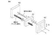
図4は、多重量子井戸層22から青色の偏光光が生じ、GaN基板1からは黄色のランダム偏光光が生じることを利用した装置の一例を示す図解図である。この装置は、図1に示す構成の窒化物半導体発光素子60と、偏光制御媒体61と、偏光フィルタ62とを備えている。When the main surface of the
FIG. 4 is an illustrative view showing an example of an apparatus using the fact that blue polarized light is generated from the multiple
窒化物半導体発光素子60と偏光フィルタ62とが対向配置されており、これらの間に、偏光制御媒体61が配置されている。偏光フィルタ62は、通過偏光方向Sに沿う偏光成分を通過させ、他の偏光成分を減衰させて実質的に遮断する。一方、窒化物半導体発光素子60から発生する青色光は、偏光方向Pに偏光している。そして、偏光方向Pと偏通過偏光方向Sが平行になるように、窒化物半導体発光素子60および偏光フィルタ62が配置されている。 The nitride semiconductor
偏光制御媒体61は、入射光の偏光状態を乱す状態と、入射光の偏光を乱さずに通過させる状態とで制御可能な媒体である。このような偏光制御媒体61の例としては、液晶を挙げることができる。
偏光制御媒体61が偏光を乱さない状態のとき、窒化物半導体発光素子60が発生する青色偏光光は、その偏光状態を保持したまま偏光制御媒体61を通過して偏光フィルタ62に至る。したがって、偏光フィルタ62でほとんど減衰されることなく、この偏光フィルタ62を通過する。一方、偏光制御媒体61が偏光を乱す状態のときには、窒化物半導体発光素子60が発生する青色偏光光は、その偏光状態が偏光制御媒体61で乱され、ランダム偏光となって偏光フィルタ62に至る。そのため、その光は偏光フィルタ62で大きく減衰されることになる。The polarization control medium 61 is a medium that can be controlled in a state in which the polarization state of incident light is disturbed and a state in which the polarization of incident light is allowed to pass through without being disturbed. An example of such a
When the
たとえば、偏光制御媒体61が偏光を乱さない状態に制御されているときに、偏光フィルタ62を通過する青色光と黄色光との光量比が1:1であるとすると、このとき、白色光が観測される。同じ条件で、偏光制御媒体61が偏光を乱す状態に制御されると、青色光が大きく減衰し、青色光と黄色光との光量比は、たとえば0.1:1などとなる。これにより、実質的に黄色光が観測されることになる。このようにして、偏光制御媒体61の状態を制御することによって、青色と黄色とに発光色を切り換えることができる。 For example, when the
偏光フィルタ62は、観測者が装着する偏光眼鏡であってもよい。この場合でも、前述の説明と同様の動作が可能である。
また、偏光制御媒体61が偏光を乱さない状態に制御されているときは、偏光眼鏡を装着しているときとしていないときとで、観測される光の色が2色に変化することになる。もっとも、このような使い方の場合には、偏光制御媒体61を設ける必要はない。The
Further, when the
以上、この発明の実施形態について説明してきたが、この発明は、さらに他の形態で実施することもできる。たとえば、前述の実施形態では、多重量子井戸層22から紫外光および青色光を発生させることにより、青色光と黄色光との混合による白色発光を行わせているが、多重量子井戸層22から紫外光のみを発生させるようにして、GaN基板1から緑色〜黄色の波長域の光を発生させ、その色光を取り出すようにしてもよい。 As mentioned above, although embodiment of this invention was described, this invention can also be implemented with another form. For example, in the above-described embodiment, by generating ultraviolet light and blue light from the multiple
また、前述の実施形態では、主としてm面を主面とするGaN基板1を用いた例について説明したが、a面を主面とするGaN基板を用いてもよい。また、(10−11)面、(10−13)面、(11−22)などといった半極性面を主面とするGaN基板を用いてもよい。
さらに、前述の実施形態では、MOCVD法によってGaN基板1上にIII族窒化物半導体をエピタキシャル成長させる例について説明したが、ハイドライド気相成長(HVPE:Hydride Vapor Phase Epitaxy)法などの他のエピタキシャル成長法が適用されてもよい。In the above-described embodiment, the example using the
Furthermore, in the above-described embodiment, an example in which a group III nitride semiconductor is epitaxially grown on the
その他、特許請求の範囲に記載された事項の範囲で種々の設計変更を施すことが可能である。 In addition, various design changes can be made within the scope of matters described in the claims.
1 GaN基板
2 III族窒化物半導体層
3 アノード電極
5 カソード電極
7 凹部
10 支持基板
11,12 配線
17 接合金属層
18 導電性材料
21 n型コンタクト層
22 多重量子井戸層
221 第1量子井戸層
222 第2量子井戸層
23 p型電子阻止層
24 p型コンタクト層
25 ファイナルバリア層
30 処理室
31 ヒータ
32 サセプタ
33 回転軸
34 回転駆動機構
35 ウエハ
36 排気配管
40 原料ガス供給路
41 窒素原料配管
42 ガリウム原料配管
43 アルミニウム原料配管
44 インジウム原料配管
45 マグネシウム原料配管
46 シリコン原料配管
51 窒素原料バルブ
52 ガリウム原料バルブ
53 アルミニウム原料バルブ
54 インジウム原料バルブ
55 マグネシウム原料バルブ
56 シリコン原料バルブ
60 窒化物半導体発光素子
61 偏光制御媒体
62 偏光フィルタDESCRIPTION OF
Claims (7)
Translated fromJapaneseこのIII族窒化物半導体基板上に成長させられたIII族窒化物半導体からなり、p型層、紫外領域の波長の光を発生する活性層およびn型層を有する発光ダイオード構造とを含む、発光素子。A group III nitride semiconductor substrate that emits light by absorbing ultraviolet light; and
A light-emitting diode structure comprising a group III nitride semiconductor grown on the group III nitride semiconductor substrate and having a p-type layer, an active layer for generating light having a wavelength in the ultraviolet region, and an n-type layer element.
前記活性層が、紫外領域の波長の光を発生する第1量子井戸層と、500nm未満の波長の可視光を発生する第2量子井戸層とを含む多重量子井戸構造を有する、請求項1または2記載の発光素子。The group III nitride semiconductor substrate absorbs ultraviolet rays and generates light having a peak wavelength of 500 nm to 600 nm;
The active layer has a multiple quantum well structure including a first quantum well layer that generates light having a wavelength in the ultraviolet region and a second quantum well layer that generates visible light having a wavelength of less than 500 nm. 2. The light emitting device according to 2.
Priority Applications (2)
| Application Number | Priority Date | Filing Date | Title |
|---|---|---|---|
| JP2007077037AJP2008235804A (en) | 2007-03-23 | 2007-03-23 | Light emitting element |
| US12/076,658US20080230766A1 (en) | 2007-03-23 | 2008-03-20 | Light emitting device |
Applications Claiming Priority (1)
| Application Number | Priority Date | Filing Date | Title |
|---|---|---|---|
| JP2007077037AJP2008235804A (en) | 2007-03-23 | 2007-03-23 | Light emitting element |
Publications (1)
| Publication Number | Publication Date |
|---|---|
| JP2008235804Atrue JP2008235804A (en) | 2008-10-02 |
Family
ID=39773781
Family Applications (1)
| Application Number | Title | Priority Date | Filing Date |
|---|---|---|---|
| JP2007077037APendingJP2008235804A (en) | 2007-03-23 | 2007-03-23 | Light emitting element |
Country Status (2)
| Country | Link |
|---|---|
| US (1) | US20080230766A1 (en) |
| JP (1) | JP2008235804A (en) |
Cited By (21)
| Publication number | Priority date | Publication date | Assignee | Title |
|---|---|---|---|---|
| WO2010052810A1 (en)* | 2008-11-06 | 2010-05-14 | パナソニック株式会社 | Nitride semiconductor element and method for manufacturing the same |
| WO2010103804A1 (en)* | 2009-03-11 | 2010-09-16 | パナソニック株式会社 | Nitride semiconductor element and method for manufacturing same |
| WO2010116703A1 (en)* | 2009-04-06 | 2010-10-14 | パナソニック株式会社 | Nitride semiconductor element and method for production thereof |
| WO2010116422A1 (en)* | 2009-04-09 | 2010-10-14 | パナソニック株式会社 | Nitride semiconductor light-emitting element, illuminating device, liquid crystal display device, method for producing nitride semiconductor light-emitting element and method for manufacturing illuminating device |
| WO2010146723A1 (en)* | 2009-06-17 | 2010-12-23 | 住友電気工業株式会社 | Iii nitride semiconductor laser element and method for manufacturing iii nitride semiconductor laser element |
| WO2010143828A3 (en)* | 2009-06-09 | 2011-03-03 | 서울반도체 주식회사 | Liquid crystal display adopting a polarized light source and a phosphor filter |
| WO2011040331A1 (en) | 2009-09-30 | 2011-04-07 | 住友電気工業株式会社 | Light-emitting element |
| US7933303B2 (en) | 2009-06-17 | 2011-04-26 | Sumitomo Electric Industries, Ltd. | Group-III nitride semiconductor laser device, and method for fabricating group-III nitride semiconductor laser device |
| WO2011077849A1 (en) | 2009-12-25 | 2011-06-30 | 住友電気工業株式会社 | Group iii nitride semiconductor laser element, method for producing group iii nitride semiconductor laser element, and epitaxial substrate |
| WO2011077856A1 (en) | 2009-12-25 | 2011-06-30 | 住友電気工業株式会社 | Group-iii nitride semiconductor laser element, and method of manufacturing group-iii nitride semiconductor laser element |
| WO2011077852A1 (en) | 2009-12-25 | 2011-06-30 | 住友電気工業株式会社 | Group-iii nitride semiconductor laser element, and method of manufacturing group-iii nitride semiconductor laser element |
| WO2011083631A1 (en)* | 2010-01-07 | 2011-07-14 | 住友電気工業株式会社 | Group iii nitride semiconductor laser element, process for producing group iii nitride semiconductor laser element, and method for evaluating damage caused by forming scribe groove |
| WO2011087127A1 (en)* | 2010-01-18 | 2011-07-21 | 住友電気工業株式会社 | Gan semiconductor light emitting element and method for manufacturing same |
| JP2012019249A (en)* | 2011-10-26 | 2012-01-26 | Sumitomo Electric Ind Ltd | Group iii nitride semiconductor laser element, and method of manufacturing group iii nitride semiconductor laser element |
| JP2012019248A (en)* | 2011-10-26 | 2012-01-26 | Sumitomo Electric Ind Ltd | Group iii nitride semiconductor laser element, and method of manufacturing group iii nitride semiconductor laser element |
| JP2012023402A (en)* | 2011-10-26 | 2012-02-02 | Sumitomo Electric Ind Ltd | Group iii nitride semiconductor laser element, and method of manufacturing group iii nitride semiconductor laser element |
| US20120199844A1 (en)* | 2009-12-25 | 2012-08-09 | Panasonic Corporation | Nitride-based semiconductor device and method for fabricating the same |
| US8729579B2 (en) | 2009-12-09 | 2014-05-20 | Panasonic Corporation | Nitride-based semiconductor light-emitting element, lighting device, liquid crystal display device, and method for producing lighting device |
| US8729587B2 (en) | 2010-04-01 | 2014-05-20 | Panasonic Corporation | Nitride semiconductor element and manufacturing method therefor |
| US8741674B2 (en) | 2009-06-17 | 2014-06-03 | Sumitomo Electric Industries, Ltd. | Group-III nitride semiconductor laser device, and method for fabricating group-III nitride semiconductor laser device |
| KR102675560B1 (en)* | 2023-01-19 | 2024-06-14 | 웨이브로드 주식회사 | Method for manufacturing ultraviolet light emitting device |
Families Citing this family (10)
| Publication number | Priority date | Publication date | Assignee | Title |
|---|---|---|---|---|
| TWI453813B (en)* | 2005-03-10 | 2014-09-21 | Univ California | Technology for growing flat semipolar gallium nitride |
| TWI455181B (en) | 2005-06-01 | 2014-10-01 | Univ California | Growth and manufacturing techniques for semi-polar (Ga, Al, In, B) N films, heterostructures and devices |
| WO2010051537A1 (en)* | 2008-10-31 | 2010-05-06 | The Regents Of The University Of California | Optoelectronic device based on non-polar and semi-polar aluminum indium nitride and aluminum indium gallium nitride alloys |
| KR100992743B1 (en)* | 2008-12-26 | 2010-11-05 | 엘지이노텍 주식회사 | Light emitting device and manufacturing method |
| US20110297956A1 (en)* | 2009-03-03 | 2011-12-08 | Panasonic Corporation | Method for manufacturing gallium nitride compound semiconductor, and semiconductor light emitting element |
| US8575592B2 (en)* | 2010-02-03 | 2013-11-05 | Cree, Inc. | Group III nitride based light emitting diode structures with multiple quantum well structures having varying well thicknesses |
| US10134948B2 (en) | 2011-02-25 | 2018-11-20 | Sensor Electronic Technology, Inc. | Light emitting diode with polarization control |
| JP5252042B2 (en)* | 2011-07-21 | 2013-07-31 | 住友電気工業株式会社 | Group III nitride semiconductor light emitting device and method for fabricating group III nitride semiconductor light emitting device |
| US11195973B1 (en)* | 2019-05-17 | 2021-12-07 | Facebook Technologies, Llc | III-nitride micro-LEDs on semi-polar oriented GaN |
| US11175447B1 (en) | 2019-08-13 | 2021-11-16 | Facebook Technologies, Llc | Waveguide in-coupling using polarized light emitting diodes |
Family Cites Families (1)
| Publication number | Priority date | Publication date | Assignee | Title |
|---|---|---|---|---|
| TW200505063A (en)* | 2003-07-10 | 2005-02-01 | Nichia Corp | Nitride semiconductor laser element |
- 2007
- 2007-03-23JPJP2007077037Apatent/JP2008235804A/enactivePending
- 2008
- 2008-03-20USUS12/076,658patent/US20080230766A1/ennot_activeAbandoned
Cited By (53)
| Publication number | Priority date | Publication date | Assignee | Title |
|---|---|---|---|---|
| JP4486701B1 (en)* | 2008-11-06 | 2010-06-23 | パナソニック株式会社 | Nitride-based semiconductor device and manufacturing method thereof |
| US8686561B2 (en) | 2008-11-06 | 2014-04-01 | Panasonic Corporation | Nitride-based semiconductor device and method for fabricating the same |
| US8648378B2 (en) | 2008-11-06 | 2014-02-11 | Panasonic Corporation | Nitride-based semiconductor device and method for fabricating the same |
| US8110851B2 (en) | 2008-11-06 | 2012-02-07 | Panasonic Corporation | Nitride-based semiconductor device and method for fabricating the same |
| WO2010052810A1 (en)* | 2008-11-06 | 2010-05-14 | パナソニック株式会社 | Nitride semiconductor element and method for manufacturing the same |
| KR101139142B1 (en) | 2008-11-06 | 2012-04-26 | 파나소닉 주식회사 | Nitride semiconductor element and method for manufacturing the same |
| US8309984B2 (en) | 2009-03-11 | 2012-11-13 | Panasonic Corporation | Nitride-based semiconductor device having electrode on m-plane |
| WO2010103804A1 (en)* | 2009-03-11 | 2010-09-16 | パナソニック株式会社 | Nitride semiconductor element and method for manufacturing same |
| JP4558846B1 (en)* | 2009-03-11 | 2010-10-06 | パナソニック株式会社 | Nitride-based semiconductor device and manufacturing method thereof |
| CN101981713B (en)* | 2009-03-11 | 2013-11-20 | 松下电器产业株式会社 | Nitride-based semiconductor device and manufacturing method thereof |
| CN101981713A (en)* | 2009-03-11 | 2011-02-23 | 松下电器产业株式会社 | Nitride semiconductor device and manufacturing method thereof |
| US8357607B2 (en) | 2009-03-11 | 2013-01-22 | Panasonic Corporation | Method for fabricating nitride-based semiconductor device having electrode on m-plane |
| WO2010116703A1 (en)* | 2009-04-06 | 2010-10-14 | パナソニック株式会社 | Nitride semiconductor element and method for production thereof |
| JP4676577B2 (en)* | 2009-04-06 | 2011-04-27 | パナソニック株式会社 | Nitride-based semiconductor device and manufacturing method thereof |
| US8058639B2 (en) | 2009-04-06 | 2011-11-15 | Panasonic Corporation | Nitride semiconductor element and method for production thereof |
| US8791473B2 (en) | 2009-04-09 | 2014-07-29 | Panasonic Corporation | Nitride semiconductor light-emitting element, illuminating device, liquid crystal display device, method for producing nitride semiconductor light-emitting element and method for manufacturing illuminating device |
| JP4815013B2 (en)* | 2009-04-09 | 2011-11-16 | パナソニック株式会社 | Nitride-based semiconductor light-emitting element, lighting device, liquid crystal display device, and manufacturing method of lighting device |
| WO2010116422A1 (en)* | 2009-04-09 | 2010-10-14 | パナソニック株式会社 | Nitride semiconductor light-emitting element, illuminating device, liquid crystal display device, method for producing nitride semiconductor light-emitting element and method for manufacturing illuminating device |
| WO2010143828A3 (en)* | 2009-06-09 | 2011-03-03 | 서울반도체 주식회사 | Liquid crystal display adopting a polarized light source and a phosphor filter |
| US7933303B2 (en) | 2009-06-17 | 2011-04-26 | Sumitomo Electric Industries, Ltd. | Group-III nitride semiconductor laser device, and method for fabricating group-III nitride semiconductor laser device |
| US8693515B2 (en) | 2009-06-17 | 2014-04-08 | Sumitomo Electric Industries, Ltd. | Group-III nitride semiconductor laser device, and method for fabricating group-III nitride semiconductor laser device |
| US8741674B2 (en) | 2009-06-17 | 2014-06-03 | Sumitomo Electric Industries, Ltd. | Group-III nitride semiconductor laser device, and method for fabricating group-III nitride semiconductor laser device |
| US8546163B2 (en) | 2009-06-17 | 2013-10-01 | Sumitomo Electric Industries, Ltd. | Group-III nitride semiconductor laser device, and method for fabricating group-III nitride semiconductor laser device |
| JP2011003660A (en)* | 2009-06-17 | 2011-01-06 | Sumitomo Electric Ind Ltd | Group iii nitride semiconductor laser element, and method of manufacturing group iii nitride semiconductor laser element |
| WO2010146723A1 (en)* | 2009-06-17 | 2010-12-23 | 住友電気工業株式会社 | Iii nitride semiconductor laser element and method for manufacturing iii nitride semiconductor laser element |
| US8823027B2 (en) | 2009-09-30 | 2014-09-02 | Sumitomo Electric Industries, Ltd. | Light emitting device |
| CN102150287A (en)* | 2009-09-30 | 2011-08-10 | 住友电气工业株式会社 | Light-emitting element |
| JP2011077351A (en)* | 2009-09-30 | 2011-04-14 | Sumitomo Electric Ind Ltd | Light emitting device |
| KR101244470B1 (en) | 2009-09-30 | 2013-03-18 | 스미토모덴키고교가부시키가이샤 | Light emitting device |
| WO2011040331A1 (en) | 2009-09-30 | 2011-04-07 | 住友電気工業株式会社 | Light-emitting element |
| US8729579B2 (en) | 2009-12-09 | 2014-05-20 | Panasonic Corporation | Nitride-based semiconductor light-emitting element, lighting device, liquid crystal display device, and method for producing lighting device |
| US8507305B2 (en) | 2009-12-25 | 2013-08-13 | Sumitomo Electric Industries, Ltd. | Group-III nitride semiconductor laser device, method of fabricating group-III nitride semiconductor laser device, and epitaxial substrate |
| WO2011077852A1 (en) | 2009-12-25 | 2011-06-30 | 住友電気工業株式会社 | Group-iii nitride semiconductor laser element, and method of manufacturing group-iii nitride semiconductor laser element |
| US20120199844A1 (en)* | 2009-12-25 | 2012-08-09 | Panasonic Corporation | Nitride-based semiconductor device and method for fabricating the same |
| WO2011077849A1 (en) | 2009-12-25 | 2011-06-30 | 住友電気工業株式会社 | Group iii nitride semiconductor laser element, method for producing group iii nitride semiconductor laser element, and epitaxial substrate |
| US8389312B2 (en) | 2009-12-25 | 2013-03-05 | Sumitomo Electric Industries, Ltd. | Group-III nitride semiconductor laser device, and method of fabricating group-III nitride semiconductor laser device |
| WO2011077856A1 (en) | 2009-12-25 | 2011-06-30 | 住友電気工業株式会社 | Group-iii nitride semiconductor laser element, and method of manufacturing group-iii nitride semiconductor laser element |
| US8401048B2 (en) | 2009-12-25 | 2013-03-19 | Sumitomo Electric Industries, Ltd. | Group-III nitride semiconductor laser device, and method of fabricating group-III nitride semiconductor laser device |
| US8772064B2 (en) | 2009-12-25 | 2014-07-08 | Sumitomo Electric Industries, Ltd. | Group-III nitride semiconductor laser device, and method of fabricating group-III nitride semiconductor laser device |
| US8748899B2 (en) | 2009-12-25 | 2014-06-10 | Panasonic Corporation | Nitride-based semiconductor device and method for fabricating the same |
| US8265113B2 (en) | 2009-12-25 | 2012-09-11 | Sumitomo Electric Industries, Ltd. | Group-III nitride semiconductor laser device, and method of fabricating group-III nitride semiconductor laser device |
| JP2011135016A (en)* | 2009-12-25 | 2011-07-07 | Sumitomo Electric Ind Ltd | Group iii nitride semiconductor laser element, and method of manufacturing group iii nitride semiconductor laser element |
| WO2011083631A1 (en)* | 2010-01-07 | 2011-07-14 | 住友電気工業株式会社 | Group iii nitride semiconductor laser element, process for producing group iii nitride semiconductor laser element, and method for evaluating damage caused by forming scribe groove |
| US8175129B2 (en) | 2010-01-07 | 2012-05-08 | Sumitomo Electric Industries, Ltd. | Group-III nitride semiconductor laser device, method of fabricating group-III nitride semiconductor laser device, and method of estimating damage from formation of scribe groove |
| US8361885B2 (en) | 2010-01-07 | 2013-01-29 | Sumitomo Electric Industries, Ltd. | Group-III nitride semiconductor laser device, method of fabricating group-III nitride semiconductor laser device, and method of estimating damage from formation of scribe groove |
| JP2011146650A (en)* | 2010-01-18 | 2011-07-28 | Sumitomo Electric Ind Ltd | Gan-group semiconductor light-emitting element and method of manufacturing the same |
| WO2011087127A1 (en)* | 2010-01-18 | 2011-07-21 | 住友電気工業株式会社 | Gan semiconductor light emitting element and method for manufacturing same |
| US8476615B2 (en) | 2010-01-18 | 2013-07-02 | Sumitomo Electric Industries, Ltd. | GaN-based semiconductor light emitting device and the method for making the same |
| US8729587B2 (en) | 2010-04-01 | 2014-05-20 | Panasonic Corporation | Nitride semiconductor element and manufacturing method therefor |
| JP2012019249A (en)* | 2011-10-26 | 2012-01-26 | Sumitomo Electric Ind Ltd | Group iii nitride semiconductor laser element, and method of manufacturing group iii nitride semiconductor laser element |
| JP2012019248A (en)* | 2011-10-26 | 2012-01-26 | Sumitomo Electric Ind Ltd | Group iii nitride semiconductor laser element, and method of manufacturing group iii nitride semiconductor laser element |
| JP2012023402A (en)* | 2011-10-26 | 2012-02-02 | Sumitomo Electric Ind Ltd | Group iii nitride semiconductor laser element, and method of manufacturing group iii nitride semiconductor laser element |
| KR102675560B1 (en)* | 2023-01-19 | 2024-06-14 | 웨이브로드 주식회사 | Method for manufacturing ultraviolet light emitting device |
Also Published As
| Publication number | Publication date |
|---|---|
| US20080230766A1 (en) | 2008-09-25 |
Similar Documents
| Publication | Publication Date | Title |
|---|---|---|
| JP2008235804A (en) | Light emitting element | |
| TWI449208B (en) | Semiconductor light emitting element and manufacturing method thereof | |
| KR101164349B1 (en) | GaN SEMICONDUCTOR OPTICAL ELEMENT, METHOD FOR MANUFACTURING GaN SEMICONDUCTOR OPTICAL ELEMENT, EPITAXIAL WAFER AND METHOD FOR GROWING GaN SEMICONDUCTOR FILM | |
| JP2008235802A (en) | Light-emitting device | |
| US7741637B2 (en) | ZnO-based semiconductor device | |
| WO2008041521A1 (en) | Light-emitting device | |
| JP2008311640A (en) | Semiconductor laser diode | |
| JP2008091488A (en) | Nitride semiconductor manufacturing method | |
| JP2009081374A (en) | Semiconductor light emitting device | |
| WO2008075581A1 (en) | Nitride semiconductor light emitting element and method for manufacturing the same | |
| JP2008153285A (en) | Nitride semiconductor device and nitride semiconductor manufacturing method | |
| JP2008198952A (en) | Group iii nitride semiconductor light emitting device | |
| KR20100023960A (en) | Nitride semiconductor light emitting element and method for manufacturing nitride semiconductor | |
| JP2009117641A (en) | Semiconductor light emitting device | |
| JP2009111012A (en) | Semiconductor light-emitting element | |
| US10116120B2 (en) | Semiconductor multilayer film mirror, vertical cavity type light-emitting element using the mirror, and methods for manufacturing the mirror and the element | |
| JP2008118049A (en) | GaN-BASED SEMICONDUCTOR LIGHT EMITTING DEVICE | |
| JP2008187044A (en) | Semiconductor laser | |
| JP2009021349A (en) | Manufacturing method of semiconductor light-emitting element, and semiconductor light-emitting element | |
| JP2008153286A (en) | Nitride semiconductor laminate structure, nitride semiconductor apparatus and manufacturing method for the nitride semiconductor laminate structure | |
| JP2009071174A (en) | Semiconductor light-emitting device | |
| JP2008218645A (en) | Light emitting device | |
| JPH11274560A (en) | Semiconductor element and manufacture thereof | |
| JP2008109021A (en) | Semiconductor light emitting element | |
| JP2008226865A (en) | Semiconductor laser diode |