JP2008233976A - Touch panel, display device, and method for manufacturing touch panel - Google Patents
Touch panel, display device, and method for manufacturing touch panelDownload PDFInfo
- Publication number
- JP2008233976A JP2008233976AJP2007068341AJP2007068341AJP2008233976AJP 2008233976 AJP2008233976 AJP 2008233976AJP 2007068341 AJP2007068341 AJP 2007068341AJP 2007068341 AJP2007068341 AJP 2007068341AJP 2008233976 AJP2008233976 AJP 2008233976A
- Authority
- JP
- Japan
- Prior art keywords
- transparent conductive
- conductive film
- touch panel
- frame wiring
- touch electrode
- Prior art date
- Legal status (The legal status is an assumption and is not a legal conclusion. Google has not performed a legal analysis and makes no representation as to the accuracy of the status listed.)
- Pending
Links
Images


Landscapes
- Position Input By Displaying (AREA)
Abstract
Translated fromJapaneseDescription
Translated fromJapanese本発明は、タッチパネル、表示装置、及びタッチパネルの製造方法に関し、特に、静電容量結合方式のタッチパネルに関するものである。 The present invention relates to a touch panel, a display device, and a method for manufacturing the touch panel, and more particularly to a capacitively coupled touch panel.
タッチパネルは、その動作原理によって、抵抗膜方式、静電容量結合方式、赤外線方式、超音波方式及び電磁誘導結合方式などに分類される。その中でも、上記抵抗膜方式及び静電容量結合方式のタッチパネルは、低コストで表示装置などに搭載可能であるので、近年よく用いられている。 The touch panel is classified into a resistance film method, a capacitive coupling method, an infrared method, an ultrasonic method, an electromagnetic inductive coupling method, and the like according to the operation principle. Among them, the resistive film type and capacitive coupling type touch panels can be mounted on a display device or the like at a low cost, and thus are frequently used in recent years.
静電容量結合方式のタッチパネルは、基板のほぼ全面に設けられた透明なタッチ電極と、タッチ電極の周端部に沿って枠状に設けられた額縁配線と、額縁配線の4隅にそれぞれ接続され、タッチ位置を検出するための位置検出回路に接続するために外部に引き出された複数の引出配線とを備え、例えば、液晶表示パネルのディスプレイ画面の前面に装着して使用される。 The capacitively coupled touch panel is connected to the transparent touch electrode provided on almost the entire surface of the substrate, the frame wiring provided in a frame shape along the peripheral edge of the touch electrode, and the four corners of the frame wiring. And a plurality of lead wires led out to connect to a position detection circuit for detecting a touch position, and is used by being mounted on the front surface of a display screen of a liquid crystal display panel, for example.
そして、静電容量結合方式のタッチパネルを備えた液晶表示パネルでは、ディスプレイ画面の前面、すなわち、タッチパネルを構成する基板の表面がタッチされることにより、タッチ電極がタッチされた点で人体の静電容量を介して接地されて、額縁配線の4隅と接地点との間の抵抗値に変化が生じ、その抵抗値の変化に基づいて位置検出回路がタッチされた位置を検出するようになっている。 In a liquid crystal display panel equipped with a capacitively coupled touch panel, the front surface of the display screen, that is, the surface of the substrate constituting the touch panel is touched, and the human body electrostatics at the point where the touch electrode is touched. The resistance value between the four corners of the frame wiring and the grounding point is grounded via the capacitor, and the position detection circuit detects the touched position based on the change in the resistance value. Yes.
例えば、特許文献1には、複数の導電性セグメントを重畳することにより抵抗値が設定された電極を有するタッチパネルが記載されている。
ところで、静電容量結合方式のタッチパネルでは、タッチ電極がタッチ位置の認識精度を高めるために高抵抗であると共に、表示装置としての表示品位を低下させないために高透過率であることが望ましく、また、額縁配線及び引出配線が低抵抗であることが望ましいので、タッチ電極が、例えば、ITO(Indium Tin Oxide)やIZO(Indium Zinc Oxide)などの透明導電膜により膜厚100Å程度で形成され、額縁配線及び引出配線が、例えば、アルミニウム及び窒化チタン膜を積層させた金属導電膜により膜厚2000Å程度で形成されている。 By the way, in the capacitive coupling type touch panel, it is desirable that the touch electrode has a high resistance in order to increase the recognition accuracy of the touch position and has a high transmittance so as not to deteriorate the display quality as a display device. Since it is desirable that the frame wiring and the lead wiring have a low resistance, the touch electrode is formed with a transparent conductive film such as ITO (Indium Tin Oxide) or IZO (Indium Zinc Oxide) with a film thickness of about 100 mm. For example, the wiring and the lead-out wiring are formed with a film thickness of about 2000 mm by a metal conductive film in which aluminum and a titanium nitride film are laminated.
ここで、タッチパネルを製造する際には、位置合わせ用のアライメントマークを額縁配線及び引出配線を構成する金属導電膜により形成することが多いので、ガラス基板(111)上に形成された額縁配線(112)の上層にタッチ電極(113)を形成することが多くなる(図11参照)。そうなると、図11に示すように、タッチ電極113を構成するために薄く形成された透明導電膜が、厚く形成された額縁配線112の側壁を覆わなくなるので、額縁配線112とタッチ電極113との導通が額縁配線112の側壁の下側部分のみで形成されて、額縁配線112とタッチ電極113との導通が不安定になるおそれがある。 Here, when manufacturing the touch panel, the alignment mark for alignment is often formed by a metal conductive film constituting the frame wiring and the lead-out wiring, so that the frame wiring formed on the glass substrate (111) ( 112), the touch electrode (113) is often formed on the upper layer (see FIG. 11). Then, as shown in FIG. 11, the transparent conductive film formed thinly to form the
本発明は、かかる点に鑑みてなされたものであり、その目的とするところは、静電容量結合方式のタッチパネルにおいて、額縁配線とタッチ電極との導通を確実にすることにある。 The present invention has been made in view of such a point, and an object thereof is to ensure conduction between the frame wiring and the touch electrode in the capacitive coupling type touch panel.
上記目的を達成するために、本発明は、タッチ電極よりも厚い透明導電層をタッチ電極を介して額縁配線を覆うようにしたものである。 In order to achieve the above object, according to the present invention, a transparent conductive layer thicker than the touch electrode covers the frame wiring via the touch electrode.
具体的に本発明に係るタッチパネルは、絶縁性基板と、上記絶縁性基板に枠状に設けられた額縁配線と、上記額縁配線に周端部が重なるように設けられ、該額縁配線よりも薄く形成された透明なタッチ電極とを備え、上記額縁配線を介する電気信号により上記タッチ電極におけるタッチ位置を検出する静電容量方式のタッチパネルであって、上記タッチ電極を介して上記額縁配線を覆うように設けられ、該タッチ電極よりも厚く形成された透明導電層を備えていることを特徴とする。 Specifically, the touch panel according to the present invention is provided with an insulating substrate, a frame wiring provided in a frame shape on the insulating substrate, and a peripheral edge portion overlapping the frame wiring, and is thinner than the frame wiring. A capacitive touch panel that detects a touch position on the touch electrode by an electric signal via the frame wiring, and covers the frame wiring via the touch electrode. And a transparent conductive layer formed to be thicker than the touch electrode.
上記の構成によれば、タッチ電極よりも厚い透明導電層がタッチ電極を介して額縁配線を覆うように設けられているので、タッチ電極をタッチした際に発生する電気信号がタッチ電極及び額縁配線の直接的な接続、並びに、タッチ電極及び額縁配線の間に透明導電層を介在させた間接的な接続の双方により、例えば、外部の位置検出回路に対して入出力されて、タッチ位置が検出されることになる。したがって、透明導電層によって、額縁配線とタッチ電極との導通が強化されるので、静電容量結合方式のタッチパネルにおいて、額縁配線とタッチ電極との導通が確実になる。 According to the above configuration, since the transparent conductive layer thicker than the touch electrode is provided so as to cover the frame wiring via the touch electrode, the electric signal generated when the touch electrode is touched is applied to the touch electrode and the frame wiring. For example, input and output to an external position detection circuit to detect the touch position by both direct connection and indirect connection with a transparent conductive layer interposed between the touch electrode and the frame wiring. Will be. Accordingly, since the conduction between the frame wiring and the touch electrode is enhanced by the transparent conductive layer, the conduction between the frame wiring and the touch electrode is ensured in the capacitive coupling type touch panel.
上記タッチ電極の厚さは、50Å〜200Åであり、上記透明導電層の厚さは、500Å〜5000Åであってもよい。 The touch electrode may have a thickness of 50 to 200 mm, and the transparent conductive layer may have a thickness of 500 to 5000 mm.
上記の構成によれば、透明導電層がタッチ電極よりも厚くなるので、本発明の作用効果が具体的に奏される。ここで、タッチ電極の厚さが50Å未満の場合には、基板面内における膜厚の均一性を保持することが困難になり、タッチ電極の厚さが200Åを超える場合には、タッチ電極の透過率が低下して、表示品位が低下するおそれがある。また、透明導電層の厚さが500Å未満の場合には、透明導電層による額縁配線とタッチ電極との導通の強化が不足して、額縁配線とタッチ電極との導通が不安定になると共に、例えば、端子部とFPC(Flexible Printed Circuit)との接続が不安定になり、透明導電層の厚さが5000Åを超える場合には、製造コストが上昇すると共に、タッチ電極との同時パターニングが困難になるおそれがある。 According to said structure, since a transparent conductive layer becomes thicker than a touch electrode, the effect of this invention is show | played concretely. Here, when the thickness of the touch electrode is less than 50 mm, it becomes difficult to maintain the uniformity of the film thickness within the substrate surface, and when the thickness of the touch electrode exceeds 200 mm, There is a possibility that the transmittance is lowered and the display quality is lowered. Further, when the thickness of the transparent conductive layer is less than 500 mm, the conduction between the frame wiring and the touch electrode by the transparent conductive layer is insufficient, and the conduction between the frame wiring and the touch electrode becomes unstable. For example, when the connection between the terminal portion and the FPC (Flexible Printed Circuit) becomes unstable and the thickness of the transparent conductive layer exceeds 5000 mm, the manufacturing cost increases and simultaneous patterning with the touch electrode becomes difficult. There is a risk.
上記タッチ電極は、酸化インジウム及び酸化スズの化合物又は酸化インジウム及び酸化亜鉛の化合物により形成されていてもよい。 The touch electrode may be formed of a compound of indium oxide and tin oxide or a compound of indium oxide and zinc oxide.
上記の構成によれば、酸化インジウム及び酸化スズの化合物(ITO)又は酸化インジウム及び酸化亜鉛の化合物(IZO)は、一般的な透明導電膜であるので、本発明の作用効果が具体的に奏される。 According to the above configuration, since the compound of indium oxide and tin oxide (ITO) or the compound of indium oxide and zinc oxide (IZO) is a general transparent conductive film, the effects of the present invention are specifically demonstrated. Is done.
上記透明導電層は、酸化インジウム及び酸化スズの化合物又は酸化インジウム及び酸化亜鉛の化合物により形成されていてもよい。 The transparent conductive layer may be formed of a compound of indium oxide and tin oxide or a compound of indium oxide and zinc oxide.
上記の構成によれば、酸化インジウム及び酸化スズの化合物(ITO)又は酸化インジウム及び酸化亜鉛の化合物(IZO)は、一般的な透明導電膜であるので、本発明の作用効果が具体的に奏される。 According to the above configuration, since the compound of indium oxide and tin oxide (ITO) or the compound of indium oxide and zinc oxide (IZO) is a general transparent conductive film, the effects of the present invention are specifically demonstrated. Is done.
上記額縁配線は、上記絶縁性基板の端部に規定された端子領域に引き出されて引出配線を構成し、上記端子領域には、上記タッチ電極及び透明導電層の少なくとも一方と同一材料で同一層に形成され、上記引出配線に接続されると共に外部に露出する端子部が設けられていてもよい。 The frame wiring is drawn out to a terminal region defined at an end of the insulating substrate to form a lead wiring, and the terminal region has the same material and the same layer as at least one of the touch electrode and the transparent conductive layer. And a terminal portion that is connected to the lead wiring and exposed to the outside.
上記の構成によれば、例えば、外部の位置検出回路に対して電気信号を入出力するために、絶縁性基板の端子領域において、引出配線をそのまま外部に露出させると、その部分から引出配線が腐食するおそれがあるものの、引出配線に接続する端子部をタッチ電極及び透明導電層の少なくとも一方を構成する安定な透明導電膜により形成して、その端子部を介して電気信号を入出力することになるので、引出配線の腐食が抑制される。これにより、腐食に強く、FPCとの接続安定性に優れた端子構造が実現する。 According to the above configuration, for example, in order to input / output an electric signal to / from an external position detection circuit, in the terminal region of the insulating substrate, when the lead wiring is exposed to the outside as it is, the lead wiring is connected from that portion. Although there is a risk of corrosion, the terminal part connected to the lead-out wiring is formed by a stable transparent conductive film that constitutes at least one of the touch electrode and the transparent conductive layer, and electric signals are input and output through the terminal part. Therefore, corrosion of the lead-out wiring is suppressed. As a result, a terminal structure that is resistant to corrosion and excellent in connection stability with the FPC is realized.
上記額縁配線は、上記タッチ電極から露出する部分を有し、上記透明導電層は、上記額縁配線の露出部分を覆うように設けられていてもよい。 The frame wiring may have a portion exposed from the touch electrode, and the transparent conductive layer may be provided so as to cover an exposed portion of the frame wiring.
上記の構成によれば、仮に、タッチ電極が極めて薄く形成されるなどして、額縁配線の側壁がタッチ電極から露出したとしても、その額縁配線の露出部分が透明導電層で覆われることにより、額縁配線とタッチ電極との導通が確実になるので、本発明の作用効果が有効に奏される。 According to the above configuration, even if the side wall of the frame wiring is exposed from the touch electrode, for example, the touch electrode is formed extremely thin, the exposed portion of the frame wiring is covered with the transparent conductive layer, Since conduction between the frame wiring and the touch electrode is ensured, the effect of the present invention is effectively exhibited.
また、本発明に係るタッチパネルは、表示パネルが対向して配置された表示装置において、特に有効である。 The touch panel according to the present invention is particularly effective in a display device in which display panels are arranged to face each other.
また、本発明に係るタッチパネルの製造方法は、透明なタッチ電極と、該タッチ電極の周端部に接続された額縁配線とを備え、該額縁配線を介する電気信号により上記タッチ電極におけるタッチ位置を検出する静電容量方式のタッチパネルを製造する方法であって、絶縁性基板に金属導電膜を成膜した後に、該金属導電膜を枠状にパターニングして、上記額縁配線を形成する額縁配線形成工程と、上記形成された額縁配線に周端部が重なるように、上記金属導電膜よりも薄い第1透明導電膜を成膜する第1透明導電膜成膜工程と、上記成膜された第1透明絶縁膜の上記額縁配線に重なる部分に、該第1透明導電膜よりも厚い第2透明導電膜を成膜する第2透明導電膜成膜工程と、上記成膜された第1透明導電膜及び第2透明導電膜を同時にパターニングして、該第1透明導電膜により上記タッチ電極を形成すると共に、該第2透明導電膜により該タッチ電極を介して上記額縁配線を覆う透明導電層を形成する透明導電膜パターニング工程とを備えることを特徴とする。 The touch panel manufacturing method according to the present invention includes a transparent touch electrode and a frame wiring connected to a peripheral end portion of the touch electrode, and the touch position on the touch electrode is determined by an electrical signal via the frame wiring. A method of manufacturing a capacitive touch panel for detection, wherein a metal conductive film is formed on an insulating substrate, and then the metal conductive film is patterned into a frame shape to form the frame wiring. A first transparent conductive film forming step of forming a first transparent conductive film that is thinner than the metal conductive film so that a peripheral edge portion overlaps the formed frame wiring, and a step of forming the first transparent conductive film A second transparent conductive film forming step of forming a second transparent conductive film thicker than the first transparent conductive film on a portion of the one transparent insulating film overlapping the frame wiring; and the first transparent conductive film formed above The film and the second transparent conductive film Forming the touch electrode with the first transparent conductive film and forming a transparent conductive layer covering the frame wiring with the second transparent conductive film through the touch electrode. It is characterized by providing.
上記の方法によれば、まず、額縁配線形成工程において、絶縁性基板上に枠状の額縁配線が形成される。続いて、第1透明導電膜成膜工程において、額縁配線形成工程で形成された額縁配線に周端部が重なるように、その額縁配線を構成する金属導電膜よりも薄い第1透明導電膜が成膜される。さらに、第2透明導電膜成膜工程において、透明導電膜成膜工程で成膜された第1透明絶縁膜の額縁配線に重なる部分に、その第1透明導電膜よりも厚い第2透明導電膜が成膜される。最後に、透明導電膜パターニング工程において、第1透明導電膜成膜工程及び第2透明導電膜成膜工程でそれぞれ成膜された第1透明導電膜及び第2透明導電膜を同時にパターニングすることにより、その第1透明導電膜によりタッチ電極が形成され、その第2透明導電膜により透明導電層が形成されることになる。ここで、製造されたタッチパネルでは、タッチ電極よりも厚い透明導電層がタッチ電極を介して額縁配線を覆うように設けられているので、タッチ電極をタッチした際に発生する電気信号がタッチ電極及び額縁配線の直接的な接続、並びに、タッチ電極及び額縁配線の間に透明導電層を介在させた間接的な接続の双方により、例えば、外部の位置検出回路に対して入出力されて、タッチ位置が検出される。したがって、透明導電層によって、額縁配線とタッチ電極との導通が強化されるので、静電容量結合方式のタッチパネルにおいて、額縁配線とタッチ電極との導通が確実になる。 According to the above method, first, frame-shaped frame wiring is formed on the insulating substrate in the frame wiring formation step. Subsequently, in the first transparent conductive film forming step, the first transparent conductive film that is thinner than the metal conductive film constituting the frame wiring is formed so that the peripheral edge portion overlaps the frame wiring formed in the frame wiring forming step. A film is formed. Further, in the second transparent conductive film forming step, a second transparent conductive film thicker than the first transparent conductive film is formed in a portion overlapping the frame wiring of the first transparent insulating film formed in the transparent conductive film forming step. Is deposited. Finally, in the transparent conductive film patterning step, by simultaneously patterning the first transparent conductive film and the second transparent conductive film formed in the first transparent conductive film formation step and the second transparent conductive film formation step, respectively. The touch electrode is formed by the first transparent conductive film, and the transparent conductive layer is formed by the second transparent conductive film. Here, in the manufactured touch panel, since the transparent conductive layer thicker than the touch electrode is provided so as to cover the frame wiring through the touch electrode, the electric signal generated when the touch electrode is touched is For example, input / output to / from an external position detection circuit by both direct connection of the frame wiring and indirect connection with a transparent conductive layer interposed between the touch electrode and the frame wiring, for example, Is detected. Accordingly, since the conduction between the frame wiring and the touch electrode is enhanced by the transparent conductive layer, the conduction between the frame wiring and the touch electrode is ensured in the capacitive coupling type touch panel.
上記額縁配線形成工程では、上記金属導電膜をパターニングして、上記額縁配線から上記絶縁性基板の端部に規定された端子領域に延びる引出配線を形成し、上記透明導電膜パターニング工程では、上記第1透明導電膜及び第2透明導電膜を同時にパターニングして、上記引出配線に接続されると共に外部に露出する端子部を形成してもよい。 In the frame wiring formation step, the metal conductive film is patterned to form a lead wiring extending from the frame wiring to a terminal region defined at an end of the insulating substrate. In the transparent conductive film patterning step, The first transparent conductive film and the second transparent conductive film may be simultaneously patterned to form a terminal portion that is connected to the lead wiring and exposed to the outside.
上記の方法によれば、例えば、外部の位置検出回路に対して電気信号を入出力するために、絶縁性基板の端子領域において、引出配線をそのまま外部に露出させると、その部分から引出配線が腐食するおそれがあるものの、額縁配線形成工程及び透明導電膜パターニング工程において、引出配線に接続する端子部をタッチ電極及び透明導電層の少なくとも一方を構成する安定な透明導電膜により形成して、その端子部を介して電気信号を入出力することになるので、引出配線の腐食が抑制される。これにより、腐食に強く、FPCとの接続安定性に優れた端子構造が実現する。 According to the above method, for example, in order to input / output an electric signal to / from an external position detection circuit, in the terminal region of the insulating substrate, when the lead wiring is exposed to the outside as it is, the lead wiring is connected from that portion. Although there is a possibility of corrosion, in the frame wiring formation process and the transparent conductive film patterning process, the terminal portion connected to the lead wiring is formed by a stable transparent conductive film constituting at least one of the touch electrode and the transparent conductive layer, Since electric signals are input and output through the terminal portion, corrosion of the lead-out wiring is suppressed. As a result, a terminal structure that is resistant to corrosion and excellent in connection stability with the FPC is realized.
本発明によれば、タッチ電極よりも厚い透明導電層がタッチ電極を介して額縁配線を覆うように設けられているので、静電容量結合方式のタッチパネルにおいて、額縁配線とタッチ電極との導通を確実にすることができる。 According to the present invention, since the transparent conductive layer thicker than the touch electrode is provided so as to cover the frame wiring via the touch electrode, in the capacitive coupling type touch panel, the frame wiring and the touch electrode are electrically connected. Can be sure.
以下、本発明の実施形態を図面に基づいて詳細に説明する。なお、以下の各実施形態では、表示装置として液晶表示装置を例示するが、本発明は、以下の各実施形態に限定されるものではない。 Hereinafter, embodiments of the present invention will be described in detail with reference to the drawings. In each of the following embodiments, a liquid crystal display device is exemplified as the display device, but the present invention is not limited to each of the following embodiments.
《発明の実施形態1》
図1〜図7は、本発明に係るタッチパネル、表示装置、及びタッチパネルの製造方法の実施形態1を示している。Embodiment 1 of the Invention
1 to 7 show Embodiment 1 of a touch panel, a display device, and a touch panel manufacturing method according to the present invention.
図1は、液晶表示装置50の概略構成図である。 FIG. 1 is a schematic configuration diagram of a liquid
液晶表示装置50は、図1に示すように、上面及び下面にそれぞれ偏光板1及び2が貼り付けられた液晶表示パネル45と、液晶表示パネル45の上方に接着層3を介して設けられたタッチパネル20aと、液晶表示パネル45の下方に拡散シート4を介して設けられ、液晶表示パネル45の表示領域に光を供給するためのバックライトユニット5とを備えている。 As shown in FIG. 1, the liquid
液晶表示パネル45は、図1に示すように、互いに対向して配置されたアクティブマトリクス基板30及び対向基板40と、それらの両基板30及び40の間に設けられた液晶層35とを備えている。 As shown in FIG. 1, the liquid
アクティブマトリクス基板30は、ガラス基板などの絶縁性基板21と、絶縁性基板21上に設けられた薄膜トランジスタ(TFT)アレイ層22と、TFTアレイ層22上に設けられた配向膜(不図示)とを備えている。ここで、TFTアレイ層22は、絶縁性基板21上に互いに平行に延びる複数のゲート線(不図示)と、各ゲート線に直交するように互いに平行に延びる複数のソース線(不図示)と、ゲート線及びソース線の各交差部分にそれぞれ設けられた複数のTFT(不図示)と、各TFTにそれぞれ接続された複数の画素電極(不図示)とを備えている。 The
対向基板40は、ガラス基板などの絶縁性基板31と、絶縁性基板31上に設けられたカラーフィルター層32と、カラーフィルター層32に設けられたオーバーコート層(不図示)と、オーバーコート層上に設けられた共通電極33と、共通電極33上に設けられた配向膜(不図示)とを備えている。 The
カラーフィルター層32は、アクティブマトリクス基板30上の各画素電極に対応して、各々、赤色、緑色又は青色に着色された複数の着色層32aと、各着色層32aの間に設けられたブラックマトリクス32bとを備えている。 The color filter layer 32 corresponds to each pixel electrode on the
液晶層35は、電気光学特性を有するネマチック液晶を含んでいる。 The
偏光板1及び2は、入射光に対して、特定方向の偏光成分のみを透過させる機能を有する光学シートである。 The polarizing plates 1 and 2 are optical sheets having a function of transmitting only a polarized light component in a specific direction with respect to incident light.
接着層3は、タッチパネル20a及び液晶表示パネル45の周端部に沿って設けられ、タッチパネル20を液晶表示パネル45に固定するためのものである。 The
拡散シート4は、バックライト5からの光を散乱及び拡散して、画面全体を均一な明るさにするための光学シートである。 The diffusion sheet 4 is an optical sheet for scattering and diffusing light from the
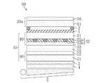
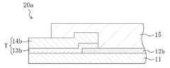
タッチパネル20aは、図1及び図2に示すように、ガラス基板などの絶縁性基板11と、絶縁性基板11上に設けられたタッチパネル層16とを備え、例えば、位置検出回路(不図示)などに接続するために後述する保護層15から露出した端子領域Pが絶縁性基板11の端部に規定されている。 As shown in FIGS. 1 and 2, the
ここで、図2は、タッチパネル20aの平面図である。そして、図3は、図2中のIII−III線に沿ったタッチパネル20aの断面図であり、図4は、図2中のIV−IV線に沿ったタッチパネル20aの断面図である。 Here, FIG. 2 is a plan view of the touch panel 20a. 3 is a cross-sectional view of the
タッチパネル層16は、図2〜図4に示すように、絶縁性基板11上に矩形枠状に設けられた額縁配線12aと、額縁配線12aの4隅から端子領域Pにそれぞれ延びるように設けられた4本の引出配線12bと、額縁配線12aに周端部が重なるように矩形状に設けられたタッチ電極13aと、タッチ電極13aを介して額縁配線12aを覆うように矩形枠状に設けられた透明導電層14aと、端子領域Pにおいて引出配線12bの端部に端子下層部13b及び端子上層部14bを順に積層して設けられた端子部Tと、タッチ電極13a、透明導電層14a及び引出配線12bを覆うように端子領域P以外の領域に設けられた保護層15とを備えている。 As shown in FIGS. 2 to 4, the
そして、タッチパネル20aは、保護層15を介してタッチ電極13aの表面がタッチされることにより、タッチ電極13aがタッチされた点で人体の静電容量を介して接地されて、額縁配線12aの4隅と接地点との間の抵抗値において変化が生じ、位置検出回路が額縁配線12aの4隅と接地点との間の抵抗値の変化に基づいてタッチされた位置を検出するようになっている。 The
ここで、図5を参照しながら、本実施形態で採用する静電容量結合方式による位置検出方法の基本原理を説明する。 Here, the basic principle of the position detection method based on the capacitive coupling method employed in the present embodiment will be described with reference to FIG.
図5では、説明を簡単にするため、タッチ電極として、電極A及びBに挟まれた1次元抵抗体が示されている。実際の表示装置では、2次元的な広がりを持つタッチ電極13aがこの1次元抵抗体と同様の機能を発揮することになる。 In FIG. 5, a one-dimensional resistor sandwiched between electrodes A and B is shown as a touch electrode for the sake of simplicity. In an actual display device, the
電極A及びBのそれぞれには、電流−電圧変換用の抵抗rが接続されている。電極A及びBは、位置検出回路に接続されている。 A current-voltage conversion resistor r is connected to each of the electrodes A and B. The electrodes A and B are connected to a position detection circuit.
電極Aとグランドとの間、及び電極Bとグランドとの間には、同相同電位の電圧(交流e)が印加されている。このとき、電極A及び電極Bは常に同電位にあるため、電極Aと電極Bとの間を電流は流れない。 A voltage having the same homologous potential (AC e) is applied between the electrode A and the ground and between the electrode B and the ground. At this time, since the electrode A and the electrode B are always at the same potential, no current flows between the electrode A and the electrode B.
そして、仮に、指で位置Xをタッチしたとすると、指によってタッチされた位置Xから電極Aまでの抵抗をR1、位置Xから電極Bまでの抵抗をR2、R=R1+R2とする。このとき、人のインピーダンスをZとし、電極Aを流れる電流をi1、電極Bを流れる電流を
i2とした場合、以下の式が成立する。If the position X is touched with a finger, the resistance from the position X touched by the finger to the electrode A is R1 , the resistance from the position X to the electrode B is R2 , and R = R1 + R2 To do. At this time, when the human impedance is Z, the current flowing through the electrode A is i1 , and the current flowing through the electrode B is i2 , the following equation is established.
e=ri1+R1i1+(i1+i2)Z (式1)
e=ri2+R2i2+(i1+i2)Z (式2)
上記の(式1)及び(式2)から、以下の(式3)及び(式4)が得られる。e = ri1 + R1 i1 + (i1 + i2 ) Z (Formula 1)
e = ri2 + R2 i2 + (i1 + i2 ) Z (Formula 2)
From the above (Formula 1) and (Formula 2), the following (Formula 3) and (Formula 4) are obtained.
i1(r+R1)=i2(r+R2) (式3)
i2=i1(r+R1)/(r+R2) (式4)
(式4)を(式1)に代入すると、以下の(式5)が得られる。i1 (r + R1 ) = i2 (r + R2 ) (Formula 3)
i2 = i1 (r + R1 ) / (r + R2 ) (Formula 4)
Substituting (Equation 4) into (Equation 1) yields (Equation 5) below.
e=ri1+R1i1+(i1+i1(r+R1)/(r+R2))Z
=i1(R(Z+r)+R1R2+2Zr+r2)/(r+R2) (式5)
上記(式5)から、以下の(式6)が得られる。e = ri1 + R1 i1 + (i1 + i1 (r + R1 ) / (r + R2 )) Z
= I1 (R (Z + r) + R1 R2 + 2Zr + r2 ) / (r + R2 ) (Formula 5)
From the above (Formula 5), the following (Formula 6) is obtained.
i1=e(r+R2)/(R(Z+r)+R1R2+2Zr+r2) (式6)
同様にして、以下の(式7)が得られる。i1 = e (r + R2 ) / (R (Z + r) + R1 R2 + 2Zr + r2 ) (Formula 6)
Similarly, the following (Formula 7) is obtained.
i2=e(r+R1)/(R(Z+r)+R1R2+2Zr+r2) (式7)
ここで、R1、R2の比を全体の抵抗Rを用いて表すと、以下の(式8)が得られる。i2 = e (r + R1 ) / (R (Z + r) + R1 R2 + 2Zr + r2 ) (Formula 7)
Here, when the ratio of R1 and R2 is expressed using the overall resistance R, the following (Equation 8) is obtained.
R1/R=(2r/R+1)i2/(i1+i2)−r/R (式8)
ここで、rとRは既知であるので、電極Aを流れる電流i1と電極Bを流れる電流i2とを測定によって求めれば、(式8)からR1/Rを決定することができる。なお、R1/Rは、指で接触した人間を含むインピーダンスZに依存しない。したがって、インピーダンスZがゼロ、無限大でない限り、(式8)が成立し、人、材料による変化、状態を無視できる。R1 / R = (2r / R + 1) i2 / (i1 + i2 ) −r / R (Formula 8)
Here, since r and R are known, if the current i1 flowing through the electrode A and the current i2 flowing through the electrode B are obtained by measurement, R1 / R can be determined from (Equation 8). Note that R1 / R does not depend on the impedance Z including a person touching with a finger. Therefore, as long as the impedance Z is not zero or infinite, (Equation 8) is established, and changes and states due to people and materials can be ignored.
次に、図6を参照しながら、上記1次元の場合における関係式を2次元の場合に適用した場合を説明する。ここで、タッチ電極13aの4隅には、図6に示すように、位置検出用電極A、B、C及びDが形成されている。これらの位置検出用電極A、B、C及びDは、各引出配線12bを介して位置検出回路に接続されている。 Next, the case where the relational expression in the one-dimensional case is applied to the two-dimensional case will be described with reference to FIG. Here, as shown in FIG. 6, position detection electrodes A, B, C, and D are formed at the four corners of the
これらの位置検出用電極A、B、C及びDには、同相同電位の交流電圧が印加され、指などの接触によって位置検出用電極A、B、C及びDに流れる電流をそれぞれi1、i2、i3及びi4とする。この場合、上記の計算と同様な計算により、以下の式が得られる。These position detection electrodes A, B, C, and D are applied with an alternating voltage of the same homogenous potential, and currents flowing through the position detection electrodes A, B, C, and D by contact with a finger or the like are respectively i1 , Let i2 , i3 and i4 . In this case, the following expression is obtained by the same calculation as the above calculation.
X=k1+k2・(i2+i3)/(i1+i2+i3+i4) (式9)
Y=k1+k2・(i2+i3)/(i1+i2+i3+i4) (式10)
ここで、Xは、タッチ電極13a上におけるタッチされた位置のX座標、Yは、タッチ電極13a上におけるタッチされた位置のY座標である。また、k1は、オフセット、k2は、倍率である。さらに、k1及びk2は、人のインピーダンスに依存しない定数である。X = k1 + k2 · (i2 + i3 ) / (i1 + i2 + i3 + i4 ) (Formula 9)
Y = k1 + k2 · (i2 + i3 ) / (i1 + i2 + i3 + i4 ) (Formula 10)
Here, X is the X coordinate of the touched position on the
そして、上記(式9)及び(式10)に基づけば各位置検出用電極A、B、C及びDを流れるi1、i2、i3及びi4の測定値から接触位置を決定することができる。Based on the above (Equation 9) and (Equation 10), the contact position is determined from the measured values of i1 , i2 , i3 and i4 flowing through the position detection electrodes A, B, C and D. Can do.
上記の例では、タッチ電極13aの4隅に電極を配置し、各電極を流れる電流を測定することにより、2次元的な広がりを持つ面上における接触位置を検出しているが、タッチ電極13aの電極数は4つに限られるものではない。2次元的な位置検出に必要な電極の最低数は3であるが、電極の数を5以上に増加させることにより、位置検出の精度を向上させることができる。 In the above example, electrodes are arranged at the four corners of the
次に、上記構成のタッチパネル20aの製造方法について、図7を用いて説明する。ここで、図7は、タッチパネルの各製造工程を示し、図3に対応する基板の断面図である。また、本実施形態の製造方法は、額縁配線形成工程、第1透明導電膜成膜工程、第2透明導電膜成膜工程、透明導電膜パターニング工程、及び保護層形成工程を備えている。 Next, a manufacturing method of the
まず、ガラス基板などの絶縁性基板11上に、図7(a)に示すように、スパッタリング法により、金属導電膜12として、例えば、アルミニウム膜(厚さ1000Å程度)、及び窒化チタン膜(厚さ1000Å程度)を連続して成膜する。 First, as shown in FIG. 7A, for example, an aluminum film (thickness of about 1000 mm) and a titanium nitride film (thickness) are formed on the insulating
続いて、フォトリソグラフィにより、金属積層膜12を枠状及びその4隅から端子領域Pに延びるようにパターニング(図2参照)して、図7(b)に示すように、額縁配線12a及び引出配線12bを形成する(額縁配線形成工程)。 Subsequently, the metal laminated
その後、絶縁性基板11の基板全体に、スパッタリング法により、図7(c)に示すように、第1透明導電膜13として、例えば、ITO(Indium Tin Oxide)膜を厚さ50Å〜200Å程度で成膜する(第1透明導電膜成膜工程)。なお、第1透明導電膜13の厚さが50Å未満の場合には、基板面内における膜厚の均一性を保持することが困難になり、第1透明導電膜13の厚さが200Åを超える場合には、タッチ電極13aの透過率が低下して、表示品位が低下するおそれがある。 Thereafter, as shown in FIG. 7C, for example, an ITO (Indium Tin Oxide) film having a thickness of about 50 to 200 mm is formed on the entire substrate of the insulating
引き続いて、第1透明導電膜13の額縁配線12a及び引出配線12bに重なる部分に、メタルマスクを用いたスパッタリング法により、図7(d)に示すように、第2透明導電膜14として、例えば、ITO(Indium Tin Oxide)膜を厚さ500Å〜5000Å程度で成膜する(第2透明導電膜成膜工程)。ここで、第1透明導電膜13の額縁配線12aよりも内側の領域には、第2透明導電膜14を成膜しないようにする。なお、第2透明導電膜14の厚さが500Å未満の場合には、透明導電層14aによる額縁配線12aとタッチ電極13aとの導通の強化が不足して、額縁配線12aとタッチ電極13aとの導通が不安定になると共に、端子部Tと例えばFPCとの接続が不安定になり、第2透明導電膜14の厚さが5000Åを超える場合には、製造コストが上昇すると共に、タッチ電極13aとの同時パターニングが困難になるおそれがある。 Subsequently, as shown in FIG. 7D, the second transparent
さらに、フォトリソグラフィにより、第1透明導電膜13及び第2透明導電膜14の積層膜を額縁配線12aに重なるように枠状に、及び端子領域Pで4つの矩形島状にパターニング(図2参照)して、図7(e)に示すように、タッチ電極13a、透明導電層14a、並びに端子下層部13b及び端子上層部14bからなる端子部T(図4参照)を形成する(透明導電膜パターニング工程)。 Further, the laminated film of the first transparent
最後に、タッチ電極13a、透明導電層14a及び引出配線12bを覆うように、メタルマスクを用いたスパッタリング法又はCVD(Chemical Vapor Deposition)法により、酸化シリコン膜(厚さ1500Å程度)などを成膜して、保護層15(図2〜図4参照)を形成する(保護層形成工程)。 Finally, a silicon oxide film (thickness of about 1500 mm) or the like is formed by a sputtering method using a metal mask or a CVD (Chemical Vapor Deposition) method so as to cover the
以上のようにして、タッチパネル層16が形成されて、タッチパネル20aを製造することができる。その後、偏光板1及び2を貼り付けた液晶表示パネル45に、タッチパネル20aを両面テープなどの接着層3により取り付けると共に、拡散シート4を介してバックライトユニット5を取り付けることにより、液晶表示装置50を製造することができる。 As described above, the
以上説明したように、本実施形態のタッチパネル20a、液晶表示装置50、及びタッチパネル20aの製造方法によれば、まず、額縁配線形成工程において、絶縁性基板11上に枠状の額縁配線12a、及びその4隅からそれぞれ延びる4本の引出配線12bが形成される。続いて、第1透明導電膜成膜工程において、額縁配線形成工程で形成された額縁配線12aに周端部が重なるように、絶縁性基板11上のほぼ基板全体に、額縁配線12aなどを構成する金属積層膜12よりも薄い第1透明導電膜13が成膜される。さらに、第2透明導電膜成膜工程において、透明導電膜成膜工程で成膜された第1透明絶縁膜13の額縁配線12aに重なる部分に、第1透明導電膜13よりも厚い第2透明導電膜14が成膜される。その後、透明導電膜パターニング工程において、第1透明導電膜成膜工程及び第2透明導電膜成膜工程でそれぞれ成膜された第1透明導電膜13及び第2透明導電膜14を同時にパターニングすることにより、第1透明導電膜13によりタッチ電極13aが形成され、第2透明導電膜14により透明導電層14aが形成されることになる。そして、最後に保護層15を形成して製造されたタッチパネル20aでは、タッチ電極13aよりも厚い透明導電層14aがタッチ電極13aを介して額縁配線12aを覆うように設けられているので、タッチ電極13aをタッチした際に発生する電気信号がタッチ電極13a及び額縁配線12aの直接的な接続、並びに、タッチ電極13a及び額縁配線12aの間に透明導電層14aを介在させた間接的な接続の双方で、例えば、外部の位置検出回路に対して入出力されることにより、タッチ位置を検出することができる。したがって、透明導電層14aによって額縁配線12aとタッチ電極13aとの導通が強化されるので、静電容量結合方式のタッチパネルにおいて、額縁配線12aとタッチ電極13aとの導通を確実にすることができる。 As described above, according to the
また、本実施形態によれば、例えば、外部の位置検出回路に対して電気信号を入出力するために、絶縁性基板11の端子領域Pにおいて、引出配線12bをそのまま外部に露出させると、その部分から引出配線12bが腐食するおそれがあるものの、額縁配線形成工程及び透明導電膜パターニング工程において、引出配線12bに接続する端子部Tをタッチ電極13a及び透明導電層14aをそれぞれ構成する第1透明導電膜13及び第2透明導電膜14により形成して、その端子部Tを介して電気信号を入出力することになるので、引出配線12bの腐食を抑制することができる。これにより、腐食に強く、FPCとの接続安定性に優れた端子構造を実現することができる。なお、本実施形態では、第1透明導電膜13をパターニングした端子下層部13b、及び第2透明導電膜14をパターニングした端子上層部14bの2層構造の端子部Tを例示したが、本発明は、端子部Tを端子下層部13b及び端子上層部14bの一方のみにより構成してもよい。 Further, according to the present embodiment, for example, when the lead-out
また、本実施形態では、第1透明導電膜13及び第2透明導電膜14として、ITOを例示したが、IZOやその他の透明性を有する導電材料であってもよい。また、第1透明導電膜13及び第2透明導電膜14は、互いに異なる導電材料であってもよい。 In the present embodiment, ITO is exemplified as the first transparent
また、本実施形態では、透明導電層14aによってタッチ電極13aを介して額縁配線12aを覆う構成を例示したが、本発明は、金属導電膜などの不透明な導電膜によって額縁配線12aを覆ってもよい。 Further, in the present embodiment, the configuration in which the
《発明の実施形態2》
図8は、本実施形態の液晶表示装置を構成するタッチパネル20bの図3に対応する断面図である。なお、以下の各実施形態において、図1〜図7と同じ部分については同じ符号を付して、その詳細な説明を省略する。<< Embodiment 2 of the Invention >>
FIG. 8 is a cross-sectional view corresponding to FIG. 3 of the
上記実施形態1のタッチパネル20aでは、タッチ電極13aが図3に示すように額縁配線12aを覆っていたが、本実施形態のタッチパネル20bでは、タッチ電極13aに対応するタッチ電極13cが図8に示すように額縁配線12aの側壁を覆ってないため、額縁配線12aがタッチ電極13cから露出していると共に、その露出部分が透明導電層14cに覆われている。 In the
本実施形態のタッチパネル20bによれば、仮に、タッチ電極13cが薄く形成されるなどして、額縁配線12aの側壁がタッチ電極13cから露出したとしても、その額縁配線12aの露出部分が透明導電層14cで覆われることにより、額縁配線12aとタッチ電極13cとの導通を確実にすることができる。 According to the
《その他の実施形態》
上記各実施形態では、絶縁性基板11とタッチ電極13a及び13cとの間に額縁配線12aが配置されていたが、図9に示すように、タッチ電極13a及び13cに対応するタッチ電極13dの上層に額縁配線12aが配置されていてもよい。ここで、図9は、本実施形態の液晶表示装置を構成するタッチパネル20cの図3に対応する断面図であり、図10は、タッチパネル20cの図4に対応する断面図である。<< Other Embodiments >>
In each of the above embodiments, the
タッチパネル20cでは、図9及び図10に示すように、絶縁性基板11上に矩形状に設けられたタッチ電極13dと、タッチ電極13dの周端部に矩形枠状に設けられた額縁配線12aと、額縁配線12aの4隅から端子領域Pにそれぞれ延びるように設けられた4本の引出配線12bと、端子領域Pにおいて引出配線12bの端部に端子下層部13e及び端子上層部14eを順に積層して設けられた端子部Tと、タッチ電極13c、額縁配線12a及び引出配線12bを覆うように設けられた保護層15とを備えている。 In the
また、タッチパネル20cは、上記実施形態1で説明した製造工程を、第1透明導電膜成膜工程、第2透明導電膜成膜工程、透明導電膜パターニング工程、額縁配線形成工程及び保護層形成工程の順に行うことにより、製造することができる。 The
本実施形態のタッチパネル20cによれば、額縁配線12aの下面全体がタッチ電極13aの上面に当接されているので、タッチ電極13cと額縁配線12aとの導通を確実にすることができ、また、引出配線12bに接続する端子部Tが安定な透明導電膜により形成されて保護層15から露出しているので、引出配線12bの腐食を抑制することができる。これにより、腐食に強く、FPCとの接続安定性に優れた端子構造を実現することができる。 According to the
なお、上記各実施形態では、タッチパネルを備えた表示装置として、液晶表示装置を例示したが、プラズマディスプレイ、無機又は有機EL(Electro Luminescence)表示装置など、種々の表示装置にも適用することができる。 In each of the above embodiments, a liquid crystal display device is exemplified as a display device provided with a touch panel. However, the present invention can also be applied to various display devices such as a plasma display and an inorganic or organic EL (Electro Luminescence) display device. .
以上説明したように、本発明は、透明導電膜の積層膜をフォトリソグラフィによりパターニングして、額縁配線とタッチ電極との導通を確実にするので、フォトリソグラフィを用いて製造されるタッチパネルについて有用である。 As described above, the present invention is useful for a touch panel manufactured using photolithography because a laminated film of transparent conductive films is patterned by photolithography to ensure conduction between the frame wiring and the touch electrode. is there.
P 端子領域
T 端子部
11 絶縁性基板
12a 額縁配線
12b 引出配線
13a,13c,13d タッチ電極
14a,14c 透明導電層
15 保護層
20a〜20c タッチパネル
45 液晶表示パネル
50 液晶表示装置P terminal region T
Claims (9)
Translated fromJapanese上記絶縁性基板に枠状に設けられた額縁配線と、
上記額縁配線に周端部が重なるように設けられ、該額縁配線よりも薄く形成された透明なタッチ電極とを備え、
上記額縁配線を介する電気信号により上記タッチ電極におけるタッチ位置を検出する静電容量方式のタッチパネルであって、
上記タッチ電極を介して上記額縁配線を覆うように設けられ、該タッチ電極よりも厚く形成された透明導電層を備えていることを特徴とするタッチパネル。An insulating substrate;
Frame wiring provided in a frame shape on the insulating substrate;
A transparent touch electrode provided so that a peripheral end overlaps the frame wiring, and formed thinner than the frame wiring;
A capacitive touch panel that detects a touch position on the touch electrode by an electrical signal through the frame wiring,
A touch panel comprising a transparent conductive layer provided so as to cover the frame wiring via the touch electrode and formed thicker than the touch electrode.
上記タッチ電極の厚さは、50Å〜200Åであり、
上記透明導電層の厚さは、500Å〜5000Åであることを特徴とするタッチパネル。In the touch panel as described in Claim 1,
The touch electrode has a thickness of 50 to 200 mm.
The thickness of the said transparent conductive layer is 500 to 5000 mm, The touch panel characterized by the above-mentioned.
上記タッチ電極は、酸化インジウム及び酸化スズの化合物又は酸化インジウム及び酸化亜鉛の化合物により形成されていることを特徴とするタッチパネル。In the touch panel as described in Claim 1,
The touch electrode is formed of a compound of indium oxide and tin oxide or a compound of indium oxide and zinc oxide.
上記透明導電層は、酸化インジウム及び酸化スズの化合物又は酸化インジウム及び酸化亜鉛の化合物により形成されていることを特徴とするタッチパネル。In the touch panel as described in Claim 1,
The touch panel, wherein the transparent conductive layer is formed of a compound of indium oxide and tin oxide or a compound of indium oxide and zinc oxide.
上記額縁配線は、上記絶縁性基板の端部に規定された端子領域に引き出されて引出配線を構成し、
上記端子領域には、上記タッチ電極及び透明導電層の少なくとも一方と同一材料で同一層に形成され、上記引出配線に接続されると共に外部に露出する端子部が設けられていることを特徴とするタッチパネル。In the touch panel as described in Claim 1,
The frame wiring is drawn out to a terminal region defined at an end of the insulating substrate to constitute a lead wiring,
The terminal region is formed with the same material as at least one of the touch electrode and the transparent conductive layer in the same layer, and is provided with a terminal portion that is connected to the lead wiring and exposed to the outside. Touch panel.
上記額縁配線は、上記タッチ電極から露出する部分を有し、
上記透明導電層は、上記額縁配線の露出部分を覆うように設けられていることを特徴とするタッチパネル。In the touch panel as described in Claim 1,
The frame wiring has a portion exposed from the touch electrode,
The touch panel, wherein the transparent conductive layer is provided so as to cover an exposed portion of the frame wiring.
上記タッチパネルに対向して配置された表示パネルとを備えていることを特徴とする表示装置。A touch panel according to claim 1;
And a display panel disposed opposite to the touch panel.
絶縁性基板に金属導電膜を成膜した後に、該金属導電膜を枠状にパターニングして、上記額縁配線を形成する額縁配線形成工程と、
上記形成された額縁配線に周端部が重なるように、上記金属導電膜よりも薄い第1透明導電膜を成膜する第1透明導電膜成膜工程と、
上記成膜された第1透明絶縁膜の上記額縁配線に重なる部分に、該第1透明導電膜よりも厚い第2透明導電膜を成膜する第2透明導電膜成膜工程と、
上記成膜された第1透明導電膜及び第2透明導電膜を同時にパターニングして、該第1透明導電膜により上記タッチ電極を形成すると共に、該第2透明導電膜により該タッチ電極を介して上記額縁配線を覆う透明導電層を形成する透明導電膜パターニング工程とを備えることを特徴とするタッチパネルの製造方法。A method of manufacturing a capacitive touch panel comprising a transparent touch electrode and a frame wiring connected to a peripheral end of the touch electrode, and detecting a touch position on the touch electrode by an electrical signal via the frame wiring Because
A frame wiring forming step of forming the frame wiring by patterning the metal conductive film after forming a metal conductive film on an insulating substrate,
A first transparent conductive film forming step of forming a first transparent conductive film that is thinner than the metal conductive film so that a peripheral edge overlaps the frame wiring formed above;
A second transparent conductive film forming step of forming a second transparent conductive film thicker than the first transparent conductive film on a portion of the first transparent insulating film formed to overlap the frame wiring;
The first transparent conductive film and the second transparent conductive film thus formed are simultaneously patterned to form the touch electrode by the first transparent conductive film, and through the touch electrode by the second transparent conductive film. A method for manufacturing a touch panel, comprising: a transparent conductive film patterning step for forming a transparent conductive layer covering the frame wiring.
上記額縁配線形成工程では、上記金属導電膜をパターニングして、上記額縁配線から上記絶縁性基板の端部に規定された端子領域に延びる引出配線を形成し、
上記透明導電膜パターニング工程では、上記第1透明導電膜及び第2透明導電膜を同時にパターニングして、上記引出配線に接続されると共に外部に露出する端子部を形成することを特徴とするタッチパネルの製造方法。In the manufacturing method of the touch panel according to claim 8,
In the frame wiring forming step, the metal conductive film is patterned to form a lead wiring extending from the frame wiring to a terminal region defined at an end of the insulating substrate,
In the transparent conductive film patterning step, the first transparent conductive film and the second transparent conductive film are simultaneously patterned to form a terminal portion that is connected to the lead wiring and exposed to the outside. Production method.
Priority Applications (1)
| Application Number | Priority Date | Filing Date | Title |
|---|---|---|---|
| JP2007068341AJP2008233976A (en) | 2007-03-16 | 2007-03-16 | Touch panel, display device, and method for manufacturing touch panel |
Applications Claiming Priority (1)
| Application Number | Priority Date | Filing Date | Title |
|---|---|---|---|
| JP2007068341AJP2008233976A (en) | 2007-03-16 | 2007-03-16 | Touch panel, display device, and method for manufacturing touch panel |
Publications (1)
| Publication Number | Publication Date |
|---|---|
| JP2008233976Atrue JP2008233976A (en) | 2008-10-02 |
Family
ID=39906728
Family Applications (1)
| Application Number | Title | Priority Date | Filing Date |
|---|---|---|---|
| JP2007068341APendingJP2008233976A (en) | 2007-03-16 | 2007-03-16 | Touch panel, display device, and method for manufacturing touch panel |
Country Status (1)
| Country | Link |
|---|---|
| JP (1) | JP2008233976A (en) |
Cited By (26)
| Publication number | Priority date | Publication date | Assignee | Title |
|---|---|---|---|---|
| JP2010170530A (en)* | 2008-12-26 | 2010-08-05 | Sumitomo Metal Mining Co Ltd | Capacitive touch panel, method for manufacturing the same, and liquid crystal display apparatus provided with the touch panel |
| JP2010287090A (en)* | 2009-06-12 | 2010-12-24 | Toppan Printing Co Ltd | Electrode plate for capacitive touch panel |
| KR101013037B1 (en) | 2010-06-16 | 2011-02-14 | (주)삼원에스티 | Touch panel sensor |
| WO2011033907A1 (en)* | 2009-09-15 | 2011-03-24 | シャープ株式会社 | Touch panel and display device provided with same |
| WO2011052392A1 (en) | 2009-10-30 | 2011-05-05 | シャープ株式会社 | Display device with touch panel |
| WO2011065292A1 (en) | 2009-11-26 | 2011-06-03 | シャープ株式会社 | Manufacturing method of touch panel, and manufacturing method of display device provided with touch panel |
| JP2011128932A (en)* | 2009-12-18 | 2011-06-30 | Sony Corp | Electro-optical device, method of manufacturing the same, and electronic apparatus |
| JP2011170252A (en)* | 2010-02-22 | 2011-09-01 | Dainippon Printing Co Ltd | Method for manufacturing of color filter with touch panel sensor integrated therein |
| WO2011159107A3 (en)* | 2010-06-16 | 2012-02-16 | (주)삼원에스티 | Touch panel sensor |
| WO2012008704A3 (en)* | 2010-07-12 | 2012-04-05 | 일진디스플레이(주) | Capacitative touch sensor and capacitative touch panel integerated into a window panel and including same |
| WO2012046624A1 (en)* | 2010-10-08 | 2012-04-12 | シャープ株式会社 | Electronic device |
| WO2012077320A1 (en)* | 2010-12-09 | 2012-06-14 | シャープ株式会社 | Touch panel, display device provided with same, and method for producing touch panel |
| WO2012077321A1 (en)* | 2010-12-09 | 2012-06-14 | シャープ株式会社 | Touch panel, display device provided with same, and method for producing touch panel |
| WO2012105690A1 (en)* | 2011-02-04 | 2012-08-09 | 信越ポリマー株式会社 | Capacitive sensor sheet and manufacturing method of same |
| WO2012117692A1 (en)* | 2011-02-28 | 2012-09-07 | シャープ株式会社 | Electrode substrate and display device and touch panel comprising same |
| WO2013099776A1 (en)* | 2011-12-28 | 2013-07-04 | シャープ株式会社 | Touch panel and display device with touch panel |
| US8550991B2 (en) | 2009-03-04 | 2013-10-08 | Dong Sik Nam | Touch panel sensor |
| WO2014069392A1 (en)* | 2012-10-31 | 2014-05-08 | 富士フイルム株式会社 | Capacitive-type touch panel and manufacturing method for same, as well as input device |
| JP2014225294A (en)* | 2014-08-07 | 2014-12-04 | 大日本印刷株式会社 | Touch panel sensor, laminate for fabricating touch panel sensor, and method for manufacturing touch panel sensor |
| KR101528145B1 (en)* | 2008-12-11 | 2015-06-11 | 엘지디스플레이 주식회사 | Touch Panel, Method for Manufacturing the Same and Liquid Crystal Display Device Using thereof |
| US9189033B2 (en) | 2010-09-29 | 2015-11-17 | Dai Nippon Printing Co., Ltd. | Touchscreen panel sensor film and manufacturing method thereof |
| JP2016157477A (en)* | 2010-09-27 | 2016-09-01 | エルジー イノテック カンパニー リミテッド | Touch screen panel and touch screen assembly including the same |
| JP2018067099A (en)* | 2016-10-18 | 2018-04-26 | 東洋アルミニウム株式会社 | Conductive sheet for pattern less touch panel |
| JP2019082926A (en)* | 2017-10-31 | 2019-05-30 | 日本航空電子工業株式会社 | Touch panel and production method thereof |
| JP2022068085A (en)* | 2020-10-21 | 2022-05-09 | ティーピーケイ アドバンスド ソリューションズ インコーポレーテッド | Touch panel and touch device |
| US11809663B2 (en) | 2010-09-14 | 2023-11-07 | Samsung Display Co., Ltd. | Flat panel display with integrated touch screen panel |
- 2007
- 2007-03-16JPJP2007068341Apatent/JP2008233976A/enactivePending
Cited By (47)
| Publication number | Priority date | Publication date | Assignee | Title |
|---|---|---|---|---|
| KR101528145B1 (en)* | 2008-12-11 | 2015-06-11 | 엘지디스플레이 주식회사 | Touch Panel, Method for Manufacturing the Same and Liquid Crystal Display Device Using thereof |
| JP2010170530A (en)* | 2008-12-26 | 2010-08-05 | Sumitomo Metal Mining Co Ltd | Capacitive touch panel, method for manufacturing the same, and liquid crystal display apparatus provided with the touch panel |
| US8550991B2 (en) | 2009-03-04 | 2013-10-08 | Dong Sik Nam | Touch panel sensor |
| JP2010287090A (en)* | 2009-06-12 | 2010-12-24 | Toppan Printing Co Ltd | Electrode plate for capacitive touch panel |
| JPWO2011033907A1 (en)* | 2009-09-15 | 2013-02-14 | シャープ株式会社 | Touch panel and display device including the same |
| WO2011033907A1 (en)* | 2009-09-15 | 2011-03-24 | シャープ株式会社 | Touch panel and display device provided with same |
| WO2011052392A1 (en) | 2009-10-30 | 2011-05-05 | シャープ株式会社 | Display device with touch panel |
| WO2011065292A1 (en) | 2009-11-26 | 2011-06-03 | シャープ株式会社 | Manufacturing method of touch panel, and manufacturing method of display device provided with touch panel |
| EP2492780A4 (en)* | 2009-11-26 | 2013-05-22 | Sharp Kk | Manufacturing method of touch panel, and manufacturing method of display device provided with touch panel |
| US8709265B2 (en) | 2009-11-26 | 2014-04-29 | Sharp Kabushiki Kaisha | Method for manufacturing touch panel and method for manufacturing display device provided with touch panel |
| JP2011128932A (en)* | 2009-12-18 | 2011-06-30 | Sony Corp | Electro-optical device, method of manufacturing the same, and electronic apparatus |
| JP2011170252A (en)* | 2010-02-22 | 2011-09-01 | Dainippon Printing Co Ltd | Method for manufacturing of color filter with touch panel sensor integrated therein |
| WO2011159107A3 (en)* | 2010-06-16 | 2012-02-16 | (주)삼원에스티 | Touch panel sensor |
| KR101013037B1 (en) | 2010-06-16 | 2011-02-14 | (주)삼원에스티 | Touch panel sensor |
| CN103097993A (en)* | 2010-06-16 | 2013-05-08 | 三元St株式会社 | Touch panel sensor |
| WO2012008704A3 (en)* | 2010-07-12 | 2012-04-05 | 일진디스플레이(주) | Capacitative touch sensor and capacitative touch panel integerated into a window panel and including same |
| TWI464655B (en)* | 2010-07-12 | 2014-12-11 | Iljin Display Co Ltd | Electrostatic capacitance touch sensor and including the electrostatic capacitance of the touch sensor with a window panel integrated electrostatic capacitance touchpad |
| CN103052932A (en)* | 2010-07-12 | 2013-04-17 | 日进显示器株式会社 | Capacitative touch sensor and capacitative touch panel integerated into a window panel and including same |
| US11809663B2 (en) | 2010-09-14 | 2023-11-07 | Samsung Display Co., Ltd. | Flat panel display with integrated touch screen panel |
| US12321555B2 (en) | 2010-09-14 | 2025-06-03 | Samsung Display Co., Ltd. | Flat panel display with integrated touch screen panel |
| JP2016157477A (en)* | 2010-09-27 | 2016-09-01 | エルジー イノテック カンパニー リミテッド | Touch screen panel and touch screen assembly including the same |
| US9189033B2 (en) | 2010-09-29 | 2015-11-17 | Dai Nippon Printing Co., Ltd. | Touchscreen panel sensor film and manufacturing method thereof |
| WO2012046624A1 (en)* | 2010-10-08 | 2012-04-12 | シャープ株式会社 | Electronic device |
| WO2012077321A1 (en)* | 2010-12-09 | 2012-06-14 | シャープ株式会社 | Touch panel, display device provided with same, and method for producing touch panel |
| WO2012077320A1 (en)* | 2010-12-09 | 2012-06-14 | シャープ株式会社 | Touch panel, display device provided with same, and method for producing touch panel |
| JP5538567B2 (en)* | 2010-12-09 | 2014-07-02 | シャープ株式会社 | Touch panel, display device including the same, and method for manufacturing touch panel |
| JP5538566B2 (en)* | 2010-12-09 | 2014-07-02 | シャープ株式会社 | Touch panel, display device including the same, and method for manufacturing touch panel |
| CN103238130B (en)* | 2011-02-04 | 2016-06-29 | 信越聚合物株式会社 | Capacitive sensor chip and manufacturing method thereof |
| CN103238130A (en)* | 2011-02-04 | 2013-08-07 | 信越聚合物株式会社 | Capacitive sensor chip and manufacturing method thereof |
| WO2012105690A1 (en)* | 2011-02-04 | 2012-08-09 | 信越ポリマー株式会社 | Capacitive sensor sheet and manufacturing method of same |
| JP2012178149A (en)* | 2011-02-04 | 2012-09-13 | Shin Etsu Polymer Co Ltd | Capacitive sensor sheet and method for manufacturing the same |
| US9482693B2 (en) | 2011-02-04 | 2016-11-01 | Shin-Etsu Polymer Co., Ltd. | Capacitive sensor sheet and production method thereof |
| TWI569078B (en)* | 2011-02-28 | 2017-02-01 | Sharp Kk | An electrode substrate, a display device including the same, and a touch panel |
| WO2012117692A1 (en)* | 2011-02-28 | 2012-09-07 | シャープ株式会社 | Electrode substrate and display device and touch panel comprising same |
| CN103392198B (en)* | 2011-02-28 | 2015-11-25 | 夏普株式会社 | Electrode substrate and display device and touch panel having same |
| CN103392198A (en)* | 2011-02-28 | 2013-11-13 | 夏普株式会社 | Electrode substrate and display device and touch panel having same |
| JP5572757B2 (en)* | 2011-02-28 | 2014-08-13 | シャープ株式会社 | Electrode substrate, and display device and touch panel provided with the same |
| WO2013099776A1 (en)* | 2011-12-28 | 2013-07-04 | シャープ株式会社 | Touch panel and display device with touch panel |
| CN104024996B (en)* | 2011-12-28 | 2016-10-05 | 夏普株式会社 | Touch panel and the display device with touch panel |
| CN104024996A (en)* | 2011-12-28 | 2014-09-03 | 夏普株式会社 | Touch panel and display device with touch panel |
| WO2014069392A1 (en)* | 2012-10-31 | 2014-05-08 | 富士フイルム株式会社 | Capacitive-type touch panel and manufacturing method for same, as well as input device |
| JP2014089641A (en)* | 2012-10-31 | 2014-05-15 | Fujifilm Corp | Capacitance type touch panel, method for manufacturing the same, and input device |
| JP2014225294A (en)* | 2014-08-07 | 2014-12-04 | 大日本印刷株式会社 | Touch panel sensor, laminate for fabricating touch panel sensor, and method for manufacturing touch panel sensor |
| JP2018067099A (en)* | 2016-10-18 | 2018-04-26 | 東洋アルミニウム株式会社 | Conductive sheet for pattern less touch panel |
| JP2019082926A (en)* | 2017-10-31 | 2019-05-30 | 日本航空電子工業株式会社 | Touch panel and production method thereof |
| JP2022068085A (en)* | 2020-10-21 | 2022-05-09 | ティーピーケイ アドバンスド ソリューションズ インコーポレーテッド | Touch panel and touch device |
| JP7083930B2 (en) | 2020-10-21 | 2022-06-13 | ティーピーケイ アドバンスド ソリューションズ インコーポレーテッド | Touch panel and touch device |
Similar Documents
| Publication | Publication Date | Title |
|---|---|---|
| JP2008233976A (en) | Touch panel, display device, and method for manufacturing touch panel | |
| JP4624462B2 (en) | Display device | |
| CN110321027B (en) | Touch sensor for display with protection | |
| JP6639829B2 (en) | Display device | |
| CN102541355B (en) | Touch control display panel | |
| JP5538566B2 (en) | Touch panel, display device including the same, and method for manufacturing touch panel | |
| US9207819B2 (en) | Touch sensing display panel and touch sensing liquid crystal display panel | |
| KR101859478B1 (en) | Liquid crystal display device having touch screen | |
| EP2472362B1 (en) | Touch-sensing display panel, touch panel, touch-sensing device and touch-sensing circuit | |
| JP2008032756A (en) | Touch panel display device and touch panel | |
| CN101910984B (en) | Touch panel and display device including the touch panel | |
| US20110175846A1 (en) | Touch display panel | |
| EP3281096A1 (en) | Transparent conductive coating for capacitive touch panel or the like | |
| WO2007144993A1 (en) | Touch panel, display device and touch panel manufacturing method | |
| KR20120121705A (en) | In-cell Type Touch Panel | |
| CN102830868B (en) | Transparent adhesive unit and the touch-screen with it | |
| CN106340530B (en) | Display device | |
| KR101893111B1 (en) | Display device including sensor | |
| KR20160081039A (en) | Liquid crystal display device using in-cell touch mode and method for fabricating the same | |
| JP2010198336A (en) | Touch panel and display apparatus including the same | |
| JP2008083899A (en) | Touch panel and display device including the same | |
| KR102007662B1 (en) | Display device having minimizded bezel | |
| KR20160018894A (en) | Touch screen panel having pressure sensor | |
| CN102479008A (en) | Touch panel, its forming method and touch display device | |
| WO2008072396A1 (en) | Touch panel device, process for manufacturing the same and display apparatus |