JP2008227104A - Laser equipment and its manufacturing method - Google Patents
Laser equipment and its manufacturing methodDownload PDFInfo
- Publication number
- JP2008227104A JP2008227104AJP2007062463AJP2007062463AJP2008227104AJP 2008227104 AJP2008227104 AJP 2008227104AJP 2007062463 AJP2007062463 AJP 2007062463AJP 2007062463 AJP2007062463 AJP 2007062463AJP 2008227104 AJP2008227104 AJP 2008227104A
- Authority
- JP
- Japan
- Prior art keywords
- electrode film
- film
- electrode
- insulating film
- laser device
- Prior art date
- Legal status (The legal status is an assumption and is not a legal conclusion. Google has not performed a legal analysis and makes no representation as to the accuracy of the status listed.)
- Granted
Links
- 238000004519manufacturing processMethods0.000titleclaimsabstractdescription24
- 239000004065semiconductorSubstances0.000claimsabstractdescription89
- 239000000758substrateSubstances0.000claimsabstractdescription36
- 239000007769metal materialSubstances0.000claimsabstractdescription35
- 229910052751metalInorganic materials0.000claimsdescription58
- 239000002184metalSubstances0.000claimsdescription58
- 238000000034methodMethods0.000claimsdescription43
- 230000000149penetrating effectEffects0.000claimsdescription36
- 230000008569processEffects0.000claimsdescription23
- 230000015572biosynthetic processEffects0.000claimsdescription15
- 229910052782aluminiumInorganic materials0.000claimsdescription12
- 229910052802copperInorganic materials0.000claimsdescription12
- 229910052737goldInorganic materials0.000claimsdescription11
- 229910052709silverInorganic materials0.000claimsdescription11
- 230000035515penetrationEffects0.000claimsdescription7
- 238000004544sputter depositionMethods0.000claimsdescription7
- 229910052697platinumInorganic materials0.000claimsdescription6
- 230000003213activating effectEffects0.000claimsdescription5
- 229910052719titaniumInorganic materials0.000claimsdescription5
- 150000002500ionsChemical class0.000claimsdescription2
- 230000017525heat dissipationEffects0.000description45
- 239000000463materialSubstances0.000description29
- 239000010931goldSubstances0.000description17
- 239000000470constituentSubstances0.000description14
- 230000004048modificationEffects0.000description13
- 238000012986modificationMethods0.000description13
- 229910000679solderInorganic materials0.000description10
- 238000001994activationMethods0.000description9
- 238000005304joiningMethods0.000description9
- 230000004888barrier functionEffects0.000description8
- 238000005229chemical vapour depositionMethods0.000description6
- 238000005530etchingMethods0.000description6
- 230000004913activationEffects0.000description5
- 238000005338heat storageMethods0.000description5
- 238000002347injectionMethods0.000description5
- 239000007924injectionSubstances0.000description5
- 238000007740vapor depositionMethods0.000description5
- 229910000980Aluminium gallium arsenideInorganic materials0.000description4
- 229910001218Gallium arsenideInorganic materials0.000description4
- 230000000694effectsEffects0.000description4
- 150000002739metalsChemical class0.000description4
- 238000005498polishingMethods0.000description4
- 230000005855radiationEffects0.000description4
- 238000005253claddingMethods0.000description3
- 230000007423decreaseEffects0.000description3
- 238000010030laminatingMethods0.000description3
- VYPSYNLAJGMNEJ-UHFFFAOYSA-NSilicium dioxideChemical compoundO=[Si]=OVYPSYNLAJGMNEJ-UHFFFAOYSA-N0.000description2
- 239000000969carrierSubstances0.000description2
- 229910052804chromiumInorganic materials0.000description2
- 239000000356contaminantSubstances0.000description2
- 230000020169heat generationEffects0.000description2
- 238000010438heat treatmentMethods0.000description2
- 239000011261inert gasSubstances0.000description2
- 238000010884ion-beam techniqueMethods0.000description2
- 239000012528membraneSubstances0.000description2
- 238000001451molecular beam epitaxyMethods0.000description2
- 238000000206photolithographyMethods0.000description2
- 229910052814silicon oxideInorganic materials0.000description2
- WFKWXMTUELFFGS-UHFFFAOYSA-NtungstenChemical compound[W]WFKWXMTUELFFGS-UHFFFAOYSA-N0.000description2
- 229910052721tungstenInorganic materials0.000description2
- 239000010937tungstenSubstances0.000description2
- XLYOFNOQVPJJNP-UHFFFAOYSA-NwaterSubstancesOXLYOFNOQVPJJNP-UHFFFAOYSA-N0.000description2
- 229910017401Au—GeInorganic materials0.000description1
- 229910000530Gallium indium arsenideInorganic materials0.000description1
- 229910004298SiO 2Inorganic materials0.000description1
- 238000002109crystal growth methodMethods0.000description1
- 239000007789gasSubstances0.000description1
- PCHJSUWPFVWCPO-UHFFFAOYSA-NgoldChemical compound[Au]PCHJSUWPFVWCPO-UHFFFAOYSA-N0.000description1
- 230000006872improvementEffects0.000description1
- 229910052738indiumInorganic materials0.000description1
- 230000001678irradiating effectEffects0.000description1
- 238000003475laminationMethods0.000description1
- 239000002245particleSubstances0.000description1
- 238000007747platingMethods0.000description1
- 230000006798recombinationEffects0.000description1
- 238000005215recombinationMethods0.000description1
- 239000007787solidSubstances0.000description1
Images


Landscapes
- Semiconductor Lasers (AREA)
Abstract
Description
Translated fromJapanese本発明は、レーザ装置及びその製造方法に関するものである。 The present invention relates to a laser device and a manufacturing method thereof.
従来、半導体レーザからの放熱性を向上させるレーザ装置の構成として、例えば特許文献1が開示されている。 Conventionally, Patent Document 1 is disclosed as a configuration of a laser device that improves heat dissipation from a semiconductor laser.
特許文献1に示されるレーザ装置は、コンタクト層を貫いて活性層の近傍に至る凹部としてのメサストライプがクラッド層に形成され、メサストライプとヒートシンクとの間に伝熱材料としての金メッキ層が充填された構成となっている。
特許文献1に示される構成においては、活性層からヒートシンクに伝わる熱が、電流注入するための電極金属を必ず通る構成となっている。電極金属の構成材料としては、オーミック特性を確保するためにCr/PtやTi/Ptが一般的であるが、Cr、Ti、Ptの熱伝導率は、それぞれ90W/m・K、22W/m・K、71W/m・Kと、315W/m・Kの熱伝導率を有するAuに対して低い。したがって、電極金属が熱障壁となり、活性層からの放熱の妨げとなる。 In the configuration shown in Patent Document 1, the heat transmitted from the active layer to the heat sink always passes through the electrode metal for current injection. As a constituent material of the electrode metal, Cr / Pt and Ti / Pt are generally used to ensure ohmic characteristics. The thermal conductivity of Cr, Ti, and Pt is 90 W / m · K and 22 W / m, respectively. Low for Au with thermal conductivity of K, 71 W / m · K and 315 W / m · K. Therefore, the electrode metal becomes a thermal barrier, which prevents heat dissipation from the active layer.
本発明は上記問題点に鑑み、活性層で生じた熱を効率よく放熱することのできるレーザ装置及びその製造方法を提供することを目的とする。 In view of the above problems, an object of the present invention is to provide a laser device capable of efficiently dissipating heat generated in an active layer and a method for manufacturing the same.
上記目的を達成する為に請求項1に記載の発明は、半導体基板と、半導体基板の一面に、活性層を含む半導体層が多層に積層配置されてなる積層体と、積層体の半導体基板配置面の裏面に積層され、半導体層の積層方向に貫通する貫通部を有する絶縁膜と、貫通部を介して積層体と接触された電極と、を備えるレーザ装置である。そして、電極は、金属材料からなり、貫通部を介して絶縁膜から露出される積層体の露出部位の一部と接触された第1電極膜と、第1電極膜よりも熱伝導率の高い金属材料からなり、積層体の露出部位のうちの第1電極膜とは異なる部位及び第1電極膜と接触され、積層体からの高さが第1電極膜の高さ以上とされた第2電極膜を有することを特徴とする。 In order to achieve the above object, the invention described in claim 1 is a semiconductor substrate, a laminate in which a semiconductor layer including an active layer is laminated on one surface of the semiconductor substrate, and a semiconductor substrate arrangement of the laminate. A laser device comprising: an insulating film having a penetrating portion stacked on the back surface of the surface and penetrating in the stacking direction of the semiconductor layer; and an electrode in contact with the stacked body through the penetrating portion. The electrode is made of a metal material, and has a first electrode film that is in contact with a part of the exposed portion of the stacked body that is exposed from the insulating film through the penetrating portion, and has a higher thermal conductivity than the first electrode film. The second electrode is made of a metal material and is in contact with the first electrode film and a portion different from the first electrode film in the exposed portion of the laminate, and the height from the laminate is equal to or higher than the height of the first electrode film. It has an electrode film.
このように本発明によれば、積層体に電流注入するための電極(対をなす一方の電極)を、積層体の露出部位の一部とそれぞれ接する第1電極膜及び第2電極膜を含む複数の電極膜によって構成している。そして、第2電極膜を、第1電極膜よりも熱伝導率の高い金属材料を用いて構成するとともに、積層体からの高さを第1電極膜の高さ以上としている。したがって、活性層で生じた熱を主として第2電極膜を通じて放熱することができるので、活性層で生じた熱を従来よりも効率よく放熱することができる。 As described above, according to the present invention, the electrode for injecting current into the stacked body (one electrode forming a pair) includes the first electrode film and the second electrode film that are in contact with a part of the exposed portion of the stacked body, respectively. It consists of a plurality of electrode films. The second electrode film is configured using a metal material having a higher thermal conductivity than the first electrode film, and the height from the stacked body is set to be equal to or higher than the height of the first electrode film. Therefore, since the heat generated in the active layer can be radiated mainly through the second electrode film, the heat generated in the active layer can be radiated more efficiently than before.
なお、注入電流は、電極を構成する第1電極膜及び第2電極膜を通して積層体へ流れる。したがって、第1電極膜を構成する金属材料を、第2電極膜よりも積層体(半導体層)とのオーミック特性に優れた材料とすることで、オーミック特性を確保する(大電流注入時の発熱を抑制する)ことができる。 The injected current flows to the laminate through the first electrode film and the second electrode film that constitute the electrode. Accordingly, the metal material constituting the first electrode film is made of a material having better ohmic characteristics with the stacked body (semiconductor layer) than the second electrode film, thereby ensuring ohmic characteristics (heat generation during large current injection). Can be suppressed).
請求項1に記載の発明においては、例えば請求項2に記載のように、第1電極膜が貫通部の壁面に対して離れて配置され、第1電極膜と貫通部の壁面との隙間に第2電極膜が介在された構成としても良い。このような構成とすると、放熱経路が分散されるので、局所的な蓄熱を抑制することができる。すなわち、レーザ装置としての信頼性を向上することができる。好ましくは請求項3に記載のように、第2電極膜が隙間を全て埋めるように配置され、隙間が等間隔とされた構成とすると、放熱経路がほぼ均等に分散されるので、局所的な蓄熱をより抑制することができる。 In the first aspect of the present invention, for example, as described in the second aspect, the first electrode film is disposed away from the wall surface of the penetrating portion, and is formed in a gap between the first electrode film and the wall surface of the penetrating portion. A configuration in which the second electrode film is interposed may be employed. With such a configuration, the heat dissipation path is dispersed, so that local heat storage can be suppressed. That is, the reliability as a laser device can be improved. Preferably, as described in claim 3, when the second electrode film is arranged so as to fill all the gaps, and the gaps are equally spaced, the heat dissipation paths are almost evenly distributed. Heat storage can be further suppressed.
請求項1〜3いずれかに記載の発明においては、請求項4に記載のように、第1電極膜の積層体からの高さ(厚さ)が絶縁膜よりも低く(薄く)され、第1電極膜の積層体接触面の裏面上にも第2電極膜が配置された構成とすると良い。このような構成とすると、第2電極膜による放熱経路の断面積を増やすことができる。すなわち、放熱性をより向上することができる。好ましくは請求項5に記載のように、第1電極膜が第2電極膜によって被覆された構成とすると、放熱経路の断面積をより増やすことができるとともに、局所的な蓄熱を抑制することができる。 In the invention according to any one of claims 1 to 3, as described in claim 4, the height (thickness) of the first electrode film from the stacked body is lower (thinner) than the insulating film, A configuration in which the second electrode film is also disposed on the back surface of the laminate contact surface of the one electrode film is preferable. With such a configuration, the cross-sectional area of the heat radiation path by the second electrode film can be increased. That is, heat dissipation can be further improved. Preferably, as described in claim 5, when the first electrode film is covered with the second electrode film, the cross-sectional area of the heat dissipation path can be increased, and local heat storage can be suppressed. it can.
請求項5に記載の発明においては、請求項6に記載のように、第2電極膜が絶縁膜の積層体接触面の裏面に積層された構成としても良い。このように、貫通部内だけでなく、絶縁膜上にも第2電極膜が配置された構成とすると、放熱経路の断面積をさらに増やすことができる。 In a fifth aspect of the present invention, as described in the sixth aspect, the second electrode film may be laminated on the back surface of the insulating film laminate contact surface. As described above, when the second electrode film is arranged not only in the through portion but also on the insulating film, the cross-sectional area of the heat dissipation path can be further increased.
請求項6に記載の発明においては、請求項7に記載のように、ヒートシンクをさらに備え、第2電極膜は絶縁膜側の面の裏面が平坦とされており、該裏面にヒートシンクが直接接合された構成とすると良い。このような構成とすると、熱伝導率の高い金属材料からなる第2電極膜を介して、活性層で生じた熱をヒートシンクに効率よく放熱することができる。したがって、放熱性をより向上することができる。なお、第2電極膜とヒートシンクとを例えばはんだを介して接合すると、はんだにおける粒界の存在や粒径の不均一性から、はんだが熱障壁となって放熱性が低下してしまう。これに対し、請求項7に記載の発明においては、第2電極膜とヒートシンクとが直接接合されている。したがって、はんだのような熱障壁を介さないので、放熱性をより向上することができる。 In a sixth aspect of the present invention, as in the seventh aspect, a heat sink is further provided, and the second electrode film has a flat rear surface on the insulating film side, and the heat sink is directly bonded to the rear surface. It is good to have the structure made. With such a configuration, heat generated in the active layer can be efficiently radiated to the heat sink via the second electrode film made of a metal material having high thermal conductivity. Therefore, heat dissipation can be further improved. Note that, when the second electrode film and the heat sink are joined via, for example, solder, the solder becomes a thermal barrier due to the presence of grain boundaries in the solder and the non-uniformity of the grain size, and heat dissipation is reduced. On the other hand, in the invention according to claim 7, the second electrode film and the heat sink are directly bonded. Therefore, heat dissipation can be further improved because a thermal barrier such as solder is not interposed.
なお、請求項7に記載の発明においては、例えば請求項8に記載のように、第2電極膜の構成材料として、Au、Cu、Al、Agのいずれかを採用すると良い。これらの金属は、熱伝導率が高く、展性、延性に優れているので、放熱性の向上とヒートシンクとの接合を両立することができる。 In the invention described in claim 7, for example, as described in claim 8, any one of Au, Cu, Al, and Ag is preferably used as the constituent material of the second electrode film. Since these metals have high thermal conductivity and are excellent in malleability and ductility, it is possible to achieve both improved heat dissipation and bonding with a heat sink.
また、請求項1〜5いずれかに記載の発明においては、請求項9に記載のように、電極を構成する複数の電極膜として、第1電極膜よりも熱伝導率が高く、且つ、第2電極膜よりも展性、延性に優れた金属材料からなる第3電極膜を有し、第3電極膜が、貫通部を含む絶縁膜上に積層されて、第1電極膜及び第2電極膜のうち、少なくとも第2電極膜と接触された構成としても良い。このような構成としても、放熱経路の断面積をさらに増やすことができる。 In the invention according to any one of claims 1 to 5, as described in claim 9, the plurality of electrode films constituting the electrode have higher thermal conductivity than the first electrode film, and A third electrode film made of a metal material that is more malleable and ductile than the two-electrode film, and the third electrode film is laminated on the insulating film including the penetrating portion to form the first electrode film and the second electrode; It is good also as a structure contacted with the 2nd electrode film at least among the films | membranes. Even with such a configuration, the cross-sectional area of the heat dissipation path can be further increased.
請求項9に記載の発明においては、請求項10に記載のように、ヒートシンクをさらに備え、第3電極膜は絶縁膜側の面の裏面が平坦とされており、該裏面にヒートシンクが直接接合された構成とすると良い。このような構成とすると、熱伝導率の高い金属材料からなる第3電極膜を介して、活性層で生じた熱をヒートシンクに効率よく放熱することができる。また、第3電極膜の絶縁膜側の面の裏面を平坦とし、熱障壁となるはんだを介さずに第3電極膜とヒートシンクとを直接接合しているので、放熱性をより向上することができる。また、第3電極膜が第2電極膜よりも展性、延性に優れた金属材料からなるので、ヒートシンクと直接接合しやすい。 In a ninth aspect of the present invention, as in the tenth aspect, the apparatus further includes a heat sink, and the back surface of the surface on the insulating film side of the third electrode film is flat, and the heat sink is directly bonded to the back surface. It is good to have the structure made. With such a configuration, the heat generated in the active layer can be efficiently radiated to the heat sink through the third electrode film made of a metal material having high thermal conductivity. Further, the back surface of the surface of the third electrode film on the insulating film side is flattened, and the third electrode film and the heat sink are directly joined without using a solder that becomes a thermal barrier, so that heat dissipation can be further improved. it can. Further, since the third electrode film is made of a metal material that is more malleable and ductile than the second electrode film, it can be easily joined directly to the heat sink.
なお、請求項10に記載の発明においては、例えば請求項11に記載のように、第3電極膜の構成材料として、Au、Cu、Al、Agのいずれかを採用することができる。これらの金属は、熱伝導率が高く、展性、延性に優れているので、放熱性の向上とヒートシンクとの接合を両立することができる。 In the invention described in claim 10, for example, as described in claim 11, any of Au, Cu, Al, and Ag can be adopted as the constituent material of the third electrode film. Since these metals have high thermal conductivity and are excellent in malleability and ductility, it is possible to achieve both improved heat dissipation and bonding with a heat sink.
請求項7、請求項8、請求項10、及び請求項11のいずれかに記載の発明においては、例えば請求項12に記載のように、ヒートシンクが、接合側の面上に第1電極膜よりも熱伝導率が高い金属材料からなり、接合側が平坦とされた金属膜を有する構成としても良い。このような構成とすると、ヒートシンクに反りや表面の荒れなどがあっても、金属膜と第2電極膜、又は、金属膜と第3電極膜を直接接合することができる。しかしながら、金属膜を有さないヒートシンクと第2電極膜及び第3電極膜のいずれかが直接接合された構成としても良い。 In the invention according to any one of claims 7, 8, 10, and 11, as described in claim 12, for example, the heat sink is formed on the surface on the bonding side from the first electrode film. Alternatively, it may be configured to have a metal film made of a metal material having high thermal conductivity and having a flat junction side. With such a configuration, the metal film and the second electrode film, or the metal film and the third electrode film can be directly bonded even if the heat sink has a warp or a rough surface. However, a configuration in which a heat sink not having a metal film and any one of the second electrode film and the third electrode film are directly bonded may be employed.
なお、請求項12に記載の発明においては、例えば請求項13に記載のように、金属膜の構成材料として、Au、Cu、Al、Agのいずれかを採用することができる。これらの金属は、熱伝導率が高く、展性、延性に優れているので、放熱性の向上と第2電極膜及び第3電極膜のいずれかとの接合を両立することができる。 In the invention described in claim 12, for example, as described in claim 13, any of Au, Cu, Al, and Ag can be adopted as a constituent material of the metal film. Since these metals have high thermal conductivity and are excellent in malleability and ductility, it is possible to achieve both improvement in heat dissipation and bonding with either the second electrode film or the third electrode film.
請求項1〜13いずれかに記載の発明は、請求項14に記載のように、第1電極膜が、Cr/Pt又はTi/Ptからなる構成としても良い。このような構成とすると、第1電極膜によって、積層体(半導体層)に対する電極のオーミック特性を確保することができる。 The invention according to any one of claims 1 to 13 may be configured such that the first electrode film is made of Cr / Pt or Ti / Pt. With such a configuration, the first electrode film can ensure ohmic characteristics of the electrode with respect to the stacked body (semiconductor layer).
次に、請求項15に記載の発明は、レーザ装置の製造方法であって、半導体基板の一面上に、活性層を含む複数の半導体層を積層してなる積層体が形成された状態で、積層体の半導体基板配置面の裏面上に絶縁膜を形成し、絶縁膜に半導体層の積層方向に貫通する貫通部を形成する絶縁膜形成工程と、貫通部を介して絶縁膜から露出される積層体の露出部位の一部と接触し、積層体からの高さが絶縁膜の高さよりも低くなるように、貫通部内に金属材料からなる第1電極膜を形成する第1電極膜形成工程と、積層体の露出部位のうちの第1電極膜とは異なる部位と接触しつつ第1電極膜を被覆し、積層体接触面の裏面が平坦となるように、貫通部を含む絶縁膜上に第1電極膜よりも熱伝導率の高い金属材料からなる第2電極膜を形成する第2電極膜形成工程と、第2電極膜とヒートシンクの接合面をそれぞれ活性化させて、常温又は低温で第2電極膜とヒートシンクを接合する接合工程と、を備えることを特徴とする。 Next, the invention according to claim 15 is a method of manufacturing a laser device, wherein a stacked body formed by stacking a plurality of semiconductor layers including an active layer is formed on one surface of a semiconductor substrate. An insulating film is formed on the back surface of the semiconductor substrate placement surface of the stacked body, and an insulating film forming step for forming a through portion penetrating in the insulating film in the stacking direction of the semiconductor layer; and the insulating film is exposed through the through portion. A first electrode film forming step of forming a first electrode film made of a metal material in the penetrating portion so as to come into contact with a part of the exposed portion of the stacked body and to make the height from the stacked body lower than the height of the insulating film And covering the first electrode film in contact with a portion different from the first electrode film in the exposed portion of the laminate, and on the insulating film including the through-hole so that the back surface of the laminate contact surface becomes flat Forming a second electrode film made of a metal material having a higher thermal conductivity than the first electrode film. And electrode film forming step, by respectively activating the bonding surface of the second electrode layer and the heat sink, characterized in that it comprises a bonding step of bonding the second electrode layer and the heat sink at room temperature or low temperature.
このように本発明によれば、請求項7に記載された第2電極膜とヒートシンクが直接接合された構成のレーザ装置を形成することができる。なお、第2電極膜とヒートシンクの接合には、第2電極膜とヒートシンクの接合面をそれぞれ活性化させて、常温又は低温で第2電極膜とヒートシンクを直接接合する表面活性化接合法を採用する。したがって、熱障壁となるはんだなどの接続部材が存在しないので、放熱性を向上することができる。なお、表面活性化接合法は、常温の場合、常温接合法や表面活性化常温接合法(SAB法)として知られている。また、上述の低温とは、半導体レーザとヒートシンクの従来の接合温度(例えばはんだによる)よりも低い温度である。 Thus, according to the present invention, it is possible to form a laser device having a configuration in which the second electrode film described in claim 7 and the heat sink are directly bonded. For the bonding of the second electrode film and the heat sink, a surface activation bonding method is used in which the bonding surface of the second electrode film and the heat sink is activated, and the second electrode film and the heat sink are directly bonded at room temperature or low temperature. To do. Therefore, since there is no connection member such as solder serving as a thermal barrier, heat dissipation can be improved. The surface activated bonding method is known as a room temperature bonding method or a surface activated room temperature bonding method (SAB method) at room temperature. The low temperature mentioned above is a temperature lower than the conventional bonding temperature (for example, by solder) between the semiconductor laser and the heat sink.
積層体接触面の裏面が平坦な第2電極膜を形成するには、例えば請求項16に記載のように、第2電極膜形成工程において、貫通部を含む絶縁膜上に第2電極膜を積層した後、第2電極膜の絶縁膜接触面の裏面を平坦としても良い。 In order to form the second electrode film having the flat back surface of the laminate contact surface, for example, in the second electrode film forming step, the second electrode film is formed on the insulating film including the penetrating portion. After the lamination, the back surface of the insulating film contact surface of the second electrode film may be flat.
また、請求項17に記載の発明も、レーザ装置の製造方法であって、半導体基板の一面上に、活性層を含む複数の半導体層を積層してなる積層体が形成された状態で、積層体の半導体基板配置面の裏面上に絶縁膜を形成し、絶縁膜に半導体層の積層方向に貫通する貫通部を形成する絶縁膜形成工程と、貫通部を介して絶縁膜から露出される積層体の露出部位の一部と接触するように、貫通部内に金属材料からなる第1電極膜を形成する第1電極膜形成工程と、積層体の露出部位のうちの第1電極膜とは異なる部位と接触しつつ第1電極膜とも接触し、積層体からの高さが第1電極膜の高さ以上となるように、絶縁膜の少なくとも貫通部内に第1電極膜よりも熱伝導率の高い金属材料からなる第2電極膜を形成する第2電極膜形成工程と、第1電極膜及び第2電極膜の形成後、貫通部を含む絶縁膜上に、絶縁膜接触面の裏面が平坦となるように、第1電極膜よりも熱伝導率が高く、且つ、第2電極膜よりも延性に優れた金属材料からなる第3電極膜を形成する第3電極膜形成工程と、第3電極膜とヒートシンクの接合面をそれぞれ活性化させて、常温又は低温で第3電極膜とヒートシンクを接合する接合工程と、を備えることを特徴とする。 The invention as set forth in claim 17 is also a method of manufacturing a laser device, wherein a laminated body formed by laminating a plurality of semiconductor layers including an active layer is formed on one surface of a semiconductor substrate. Forming an insulating film on the back surface of the semiconductor substrate placement surface of the body, forming an insulating film through-hole that penetrates the insulating film in the stacking direction of the semiconductor layer, and laminating exposed from the insulating film through the through-hole The first electrode film forming step of forming a first electrode film made of a metal material in the penetrating part so as to contact a part of the exposed part of the body is different from the first electrode film in the exposed part of the laminate. The first electrode film is contacted with the first electrode film while being in contact with the part, and the thermal conductivity of the insulating film is higher than that of the first electrode film in at least the penetrating portion of the insulating film so that the height from the laminated body is equal to or higher than the height of the first electrode film. A second electrode film forming step of forming a second electrode film made of a high metal material; After the formation of the polar film and the second electrode film, the second electrode has a higher thermal conductivity than the first electrode film so that the back surface of the insulating film contact surface is flat on the insulating film including the penetrating portion. A third electrode film forming step of forming a third electrode film made of a metal material having superior ductility than the film; and a bonding surface between the third electrode film and the heat sink is activated, and the third electrode film is formed at room temperature or low temperature. And a joining step for joining the heat sink.
このように本発明によれば、請求項10に記載された第3電極膜とヒートシンクが直接接合された構成のレーザ装置を形成することができる。なお、第3電極膜とヒートシンクの接合には、第3電極膜とヒートシンクの接合面をそれぞれ活性化させて、常温又は低温で第3電極膜とヒートシンクを直接接合する表面活性化接合法を採用する。したがって、熱障壁となるはんだなどの接続部材が存在しないので、放熱性を向上することができる。なお、表面活性化接合法は、常温の場合、常温接合法や表面活性化常温接合法(SAB法)として知られている。また、上述の低温とは、半導体レーザとヒートシンクの従来の接合温度(例えばはんだによる)よりも低い温度である。 Thus, according to the present invention, it is possible to form a laser device having a configuration in which the third electrode film according to claim 10 and the heat sink are directly bonded. For the bonding of the third electrode film and the heat sink, a surface activated bonding method is employed in which the bonding surface of the third electrode film and the heat sink is activated, and the third electrode film and the heat sink are directly bonded at room temperature or low temperature. To do. Therefore, since there is no connection member such as solder serving as a thermal barrier, heat dissipation can be improved. The surface activated bonding method is known as a room temperature bonding method or a surface activated room temperature bonding method (SAB method) at room temperature. The low temperature mentioned above is a temperature lower than the conventional bonding temperature (for example, by solder) between the semiconductor laser and the heat sink.
絶縁膜接触面の裏面が平坦な第3電極膜を形成するには、例えば請求項18に記載のように、第3電極膜形成工程において、第1電極膜及び第2電極膜のうち、積層体からの高さが絶縁膜よりも高い部位を、絶縁膜をストッパとして除去した後、第3電極膜を形成する方法を採用しても良い。 In order to form the third electrode film having the flat back surface of the insulating film contact surface, for example, in the third electrode film forming step, a stacked layer of the first electrode film and the second electrode film is formed. A method may be employed in which the third electrode film is formed after removing a portion whose height from the body is higher than the insulating film using the insulating film as a stopper.
請求項15〜18いずれかに記載の発明においては、例えば請求項19に記載のように、第1電極形成工程において、第1電極膜を貫通部の壁面に対して離間して形成し、第2電極形成工程において、第1電極膜と貫通部の壁面との隙間に介在するように第2電極膜を形成しても良い。この場合、請求項20に記載のように、第1電極形成工程において、隙間が積層体からの絶縁膜の高さに対する第1電極膜高さの差以下となるように、第1電極膜を絶縁膜よりも低く形成し、第2電極形成工程において、貫通部内に選択的に第2電極膜を形成しても良い。これによれば、絶縁膜と面一となるように貫通部内に第2電極膜を選択的に形成することもできる。面一とした場合、研磨などの処理を不要とすることもできる。 In the invention according to any one of claims 15 to 18, for example, as described in claim 19, in the first electrode forming step, the first electrode film is formed so as to be separated from the wall surface of the penetrating portion. In the two-electrode forming step, the second electrode film may be formed so as to be interposed in the gap between the first electrode film and the wall surface of the penetrating portion. In this case, as described in claim 20, in the first electrode formation step, the first electrode film is formed so that the gap is equal to or less than the difference in height of the first electrode film with respect to the height of the insulating film from the stacked body. The second electrode film may be formed lower than the insulating film, and the second electrode film may be selectively formed in the through portion in the second electrode formation step. According to this, the second electrode film can be selectively formed in the through portion so as to be flush with the insulating film. In the case of being flush with each other, it is possible to eliminate processing such as polishing.
請求項15〜20いずれかに記載の発明においては、請求項21に記載のように、ヒートシンクの一面に第1電極膜よりも熱伝導率が高い金属材料からなり、接合側が平坦とされた金属膜を有し、接合工程において、電極膜の表面を接合面としても良い。これによれば、ヒートシンクに反りや表面の荒れなどがあっても、請求項12に記載のレーザ装置を形成することができる。 In the invention according to any one of claims 15 to 20, as described in claim 21, a metal made of a metal material having a higher thermal conductivity than the first electrode film on one surface of the heat sink and having a flat junction side It has a film | membrane, and it is good also considering the surface of an electrode film as a joining surface in a joining process. Accordingly, the laser device according to claim 12 can be formed even if the heat sink is warped or the surface is rough.
請求項15〜21いずれかに記載の発明においては、請求項22に記載のように、接合工程において、接合時の温度を100℃以下の低温とすると良い。このように100℃以下とすると、ヒートシンクと半導体基板の線膨張係数差に基づいて活性層に作用する応力を、効果的に抑制することができる。 In the invention according to any one of claims 15 to 21, as described in claim 22, in the joining step, the temperature at the time of joining may be a low temperature of 100 ° C. or less. Thus, if it is set to 100 degrees C or less, the stress which acts on an active layer based on the linear expansion coefficient difference of a heat sink and a semiconductor substrate can be suppressed effectively.
また、請求項15〜22いずれかに記載の発明においては、例えば請求項23に記載のように、接合工程において、Arイオンでスパッタリングすることにより、接合面をそれぞれ活性化させることができる。 In the invention described in any one of claims 15 to 22, for example, as described in claim 23, in the bonding step, the bonding surface can be activated by sputtering with Ar ions.
以下、本発明の実施形態を図に基づいて説明する。
(第1実施形態)
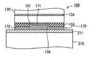
図1は、第1実施形態に係るレーザ装置のうち、半導体レーザの概略構成を示す断面図である。図2は、半導体レーザの平面図である。図3は、レーザ装置のうち、特徴部分の拡大断面図である。なお、図2においては、便宜上、第2電極膜及び第3電極膜を省略して図示している。また、図3においては、便宜上、積層体のうち、活性層以外の半導体層を省略して図示している。Hereinafter, embodiments of the present invention will be described with reference to the drawings.
(First embodiment)
FIG. 1 is a cross-sectional view showing a schematic configuration of a semiconductor laser in the laser apparatus according to the first embodiment. FIG. 2 is a plan view of the semiconductor laser. FIG. 3 is an enlarged cross-sectional view of a characteristic portion of the laser device. In FIG. 2, for convenience, the second electrode film and the third electrode film are omitted. In FIG. 3, for convenience, a semiconductor layer other than the active layer is omitted from the stack.
本実施形態に係るレーザ装置は、端面発光型ストライプ構造の半導体レーザと、活性層で生じた熱を放熱するためのヒートシンクとを一体化してなるものである。 The laser device according to this embodiment is formed by integrating a semiconductor laser having an edge-emitting stripe structure and a heat sink for radiating heat generated in an active layer.
半導体レーザは、図1に示すように、要部として、半導体基板110と、半導体基板110の一面(以下、上面と示す)に、活性層134を含む半導体層を多層に積層配置してなる積層体130と、積層体130の半導体基板配置面の裏面(以下、上面と示す)に配置され、半導体層の積層方向に貫通する貫通部151を有する絶縁膜150と、貫通部151を介して積層体130と接触された第1電極170と、半導体基板110の下面(積層体配置面の裏面)に配置された第2電極190と、を有している。このうち、第1電極170を特徴部分としている。 As shown in FIG. 1, the semiconductor laser has a
本実施形態においては、半導体基板110としてn−GaAs基板を採用している。そして半導体基板110の一面に、n−GaAsからなるバッファ層131、n−AlGaAsからなるクラッド層132、n−AlGaAsからなる光ガイド層133、InGaAsからなる活性層134、p−AlGaAsからなる光ガイド層135、p−AlGaAsからなるクラッド層136、p−GaAsからなるコンタクト層137の順で積層されて、複数の半導体層からなる積層体130が構成されている。なお、バッファ層131は結晶性を高める層、クラッド層132,136は主として活性層134の接合領域の電子密度及びホール密度を高める層、光ガイド層133,135は発光した光を活性層134に閉じ込める層、活性層134は注入されたキャリアが再結合し、該層のバンドギャップエネルギーに応じた波長の光を発光する層である。 In the present embodiment, an n-GaAs substrate is employed as the
このように構成される積層体130の上面に、絶縁膜150が配置されている。本実施形態において、絶縁膜150はシリコン酸化膜からなり、絶縁膜150の一部に、半導体層の積層方向に貫通する貫通部151が設けられている。より詳しくは、図2に示すように、貫通部151は、活性層134の積層面に平行であってレーザ光の出力方向(図1において紙面に垂直な方向)に垂直な方向の幅S(ストライプ幅S)が、レーザ光の出力方向の長さ(共振器長)よりも短い幅(例えば10μm)とされたストライプ状の溝となっている。 An insulating
そして、積層体130の上面上には、貫通部151を介して積層体130と接触するように、p型電極としての第1電極170が配置されている。この第1電極170が、特許請求の範囲に記載の電極に相当するものである。本実施形態において、第1電極170は、第1電極膜171、第2電極膜172、及び第3電極膜173からなり、貫通部151を含む絶縁膜150上に配置されている。 And on the upper surface of the
第1電極膜171は、第1電極170のうち、積層体130(コンタクト層137)に対してオーミック特性を得るための部位であり、第2電極膜172や第3電極膜173よりも積層体130に対してオーミック特性に優れる(電気的抵抗の小さい)金属材料を用いて構成されている。そして、貫通部151を介して絶縁膜150から露出される積層体130の露出部位138の一部と接触されている。 The
本実施形態においては、積層体130(コンタクト層137)に対してオーミック特性を得るべく、Cr/Ptを用いて構成されている。また、図1及び図2に示すように、ストライプ状の貫通部151の両壁面に対して離間され、両壁面との間で構成される隙間L1,L2が互いに等しくされている。また、図1に示すように、積層体130(露出部位138)からの高さ(厚さ)が、絶縁膜150よりも低く(薄く)され、露出部位138からの絶縁膜150の高さと第1電極膜171の高さの差(後述する差t)が、隙間L1,L2と等しくされている。なお、オーミック特性に優れる材料としては、上述のCr/Ptに限定されるものではなく、それ以外にも、例えばTi/Ptを構成材料とすることもできる。 In the present embodiment, Cr / Pt is used to obtain ohmic characteristics with respect to the stacked body 130 (contact layer 137). Moreover, as shown in FIG.1 and FIG.2, it is spaced apart with respect to both wall surfaces of the stripe-shaped
第2電極膜172は、第1電極170のうち、活性層134で生じた熱を半導体レーザ外(本実施形態においてはヒートシンク)に放熱するに当たり、主として貫通部151内における放熱性を向上するための部位であり、第1電極膜171よりも熱伝導率の高い金属材料を用いて構成されている。そして、絶縁膜150から露出される積層体130の露出部位138のうち、第1電極膜171とは異なる部位と接触されている。また、貫通部151内において第1電極膜171とも接触され、露出部位138からの高さが第1電極膜171の高さ以上とされている。 The
第2電極膜172の構成材料としては、単一金属を採用すると良い。複数の金属からなる構成に比べて粒界や粒径ばらつきによる熱伝導性の低下を抑制し、放熱性を向上することができる。本実施形態においては、熱伝導率が178W/m・KのW(タングステン)を用いて構成されている。ちなみに、第1電極膜171の構成材料であるCr、Pt、Tiの熱伝導率は、それぞれ90W/m・K、71W/m・K、22W/m・Kである。また、図1に示すように、第2電極膜172は、貫通部151内のみに配置されており、第1電極膜171の配置部位以外の部位を満たしている。すなわち、積層体130の露出部位138のうち、第1電極膜171の接触部位を除く部位全てに接触されている。また、露出部位138からの高さが第1電極膜171の高さよりも高くされている。さらには、第1電極膜171の積層体接触面の裏面上にも配置され、第1電極膜171の積層体接触部位以外の部位が第2電極膜172に被覆されている。 As a constituent material of the
なお、第2電極膜172の構成材料としては、上述したW以外にも、Cu(熱伝導率398W/m・K)、Al(熱伝導率237W/m・K)、Au(熱伝導率315W/m・K)、Ag(熱伝導率427W/m・K)などを採用することができる。 In addition to the W described above, the constituent material of the
第3電極膜173は、第1電極170のうち、貫通部151を通して伝達された熱をヒートシンクに効率よく放熱する部位であるとともに、ヒートシンクに半導体レーザを固定するための接合部位であり、第1電極膜171よりも熱伝導率が高く、且つ、第2電極膜172よりも展性、延性に優れた金属材料を用いて構成されている。そして、貫通部151を含む絶縁膜150上に配置されて、第1電極膜171及び第2電極膜173のうち、少なくとも第2電極膜172と接触されている。 The
本実施形態においては、熱伝導率が高く、且つ、延性,展性に優れるAuを用いて構成されている。Auの場合、ヒートシンクとの接続信頼性や放熱時の熱障壁となる酸化膜が形成されないので好ましい材料である。しかしながら、Au以外にも、Cu、Al、Agなどを採用することができる。また、第3電極膜173は、その厚さが500nm以上2000nm未満ととされており、絶縁膜150側の面の裏面が平坦とされている。 In the present embodiment, Au is used which has high thermal conductivity and is excellent in ductility and malleability. In the case of Au, a connection material with a heat sink and an oxide film that becomes a thermal barrier at the time of heat dissipation are not formed, so that Au is a preferable material. However, other than Au, Cu, Al, Ag, etc. can be employed. The
第2電極190は、第1電極170と対をなし、活性層134に対して電流を注入するための電極であり、半導体基板110の下面に配置されている。本実施形態においては、n型電極として、例えばAu−Ge/Ni/Auからなる第2電極190が配置されている。 The
図3に示すように、ヒートシンク210は、活性層134で生じた熱を半導体レーザ(レーザ装置100)の外部に放熱するためのものである。このため、熱伝導率の大きな材料を用いて構成されている。また、半導体レーザと直接接合すべく半導体レーザとの接触面が平坦とされている。本実施形態において、ヒートシンク210は、第1電極膜171を構成するWよりも熱伝導率の大きなCuを用いて平板状に構成されている。 As shown in FIG. 3, the
さらに、本実施形態においては、図3に示すように、ヒートシンク210が、接合側の面上に、第1電極膜171よりも熱伝導率が高い金属材料からなり、接合側が平坦とされた接合用金属膜211を有している。この接合用金属膜211は、特許請求の範囲に記載の金属膜に相当するものである。このように、ヒートシンク210が接合用金属膜211を有する構成とすると、ヒートシンク210の表面が反っていたり、凹凸を有していても、接合用金属膜211を接触面として、半導体レーザとヒートシンク210の接続信頼性を確保することができる。なお、放熱性と接続信頼性を両立するには、熱伝導率が高く、展性、延性に優れる材料を採用することが好ましい。このような材料としては、例えばAu、Cu、Al、Agがある。本実施形態においては、接合用金属膜211がCuからなり、ヒートシンク210と接合用金属膜211が同一材料からなるので、ヒートシンク210と接合用金属膜211の界面における放熱ロスを抑制し、これによっても放熱性を向上することができる。 Further, in the present embodiment, as shown in FIG. 3, the
次に、上述したレーザ装置100の製造方法を、図4〜図6を用いて説明する。図4は、レーザ装置の製造工程を示す断面図であり、(a)は絶縁膜形成工程、(b)は第1電極膜形成工程、(c)は第2電極膜形成工程を示している。図5(a),(b)は、レーザ装置の製造工程のうち、第3電極膜形成工程を示す断面図である。図6(a)〜(c)は、レーザ装置の製造工程のうち、接合工程を示す断面図である。なお、図4〜図6においては、便宜上、積層体のうち、活性層以外の半導体層を省略して図示している。 Next, the manufacturing method of the
先ず、MOCVD(有機金属気相成長)法やMBE(分子線エピタキシー)法などの公知の結晶成長方法を用いて半導体基板110上に活性層134を含む積層体130を形成する。積層体130の形成後、図4(a)に示すように、積層体130の上面に絶縁膜150を形成し、絶縁膜150に積層体130を構成する半導体層の積層方向に貫通する貫通部151を形成する絶縁膜形成工程を実施する。本実施形態においては、CVD法によって、積層体130の上面全面にシリコン酸化物(SiO2)からなる絶縁膜150を形成する。そして、フォトリソグラフィによって、ストライプとなる部分の絶縁膜150をエッチングして開口し、溝状の貫通部151を形成している。First, the
次に、第1電極形成工程を実施する。本実施形態においては、第1電極形成工程が大きく分けて3つの工程からなる。先ず、蒸着やスパッタなどの公知の成膜方法を用いて、図4(b)に示すように、貫通部151を介して絶縁膜150から露出される積層体130の露出部位138の一部と接触するように、貫通部151内に第1電極膜171を形成する第1電極膜形成工程を実施する。本実施形態においては、蒸着によってCr/Ptを成膜し、フォトリソグラフィによって不要部分を除去することにより、図4(b)に示すように、積層体130(露出部位138)からの高さが絶縁膜150よりも低く、貫通部151の両壁面との隙間L1,L2、及び、露出部位138からの絶縁膜150の高さと第1電極膜171の高さの差tがそれぞれ等しい第1電極膜171を形成する。 Next, a 1st electrode formation process is implemented. In the present embodiment, the first electrode forming step is roughly divided into three steps. First, using a known film formation method such as vapor deposition or sputtering, as shown in FIG. 4B, a part of the exposed
次に、図4(c)に示すように、積層体130の露出部位138のうち、第1電極膜171の接触部位とは異なる部位と接触しつつ第1電極膜171とも接触し、露出部位138からの高さが第1電極膜171の高さ以上となるように、絶縁膜150の少なくとも貫通部151内に第1電極膜171よりも熱伝導率の高い金属材料からなる第2電極膜172を形成する第2電極膜形成工程を実施する。本実施形態においては、公知の選択ダングステンCVD法によって、図4(b)に示すように、絶縁膜150以外の表面上(すなわち露出部位138及び第1電極膜171上)に、絶縁膜150と略面一となるようにW(タングステン)からなる第2電極膜172を選択的に形成する。このように選択CVD法を採用すると、選択的かつ単純な工程で、貫通部151内のみに第2電極膜172を形成することができる。なお、選択CVD法による第2電極膜172の形成は、W以外にもAlやCuで可能である。また、選択CVD法以外にも、蒸着、スパッタ、CVD法などにより第2電極膜172を形成することができる。 Next, as illustrated in FIG. 4C, the exposed
なお、本実施形態においては、第1電極膜形成工程において、貫通部151の両壁面との隙間L1,L2、及び、露出部位138からの絶縁膜150の高さと第1電極膜171の高さの差tがそれぞれ等しい第1電極膜171を形成し、第2電極膜形成工程において、絶縁膜150と略面一となるように第2電極膜172を選択的に形成する。したがって、第2電極膜形成工程終了時に、第2電極膜172と絶縁膜150との段差を極力小さくすることができるので、平坦化処理を行わなくとも、第1電極170とヒートシンク210との接続信頼性を向上することができる。しかしながら、必要に応じて平坦化処理を実施し、これによって第1電極170とヒートシンク210との接続信頼性を向上するようにしても良い。例えば、第2電極膜172の成膜後に平坦化処理を実施しても良い。一例としては、スパッタによって貫通部151内を埋めつつ絶縁膜150の表面を被覆するように第2電極膜172を成膜した後、絶縁膜150をストッパとして第2電極膜172を研磨し、平坦化しても良い。このように第2電極膜172に平坦化処理を実施すると、絶縁膜150を平坦化の基準(ストッパ)とすることができるので平坦化しやすい。また、本実施形態に示すように、第1電極170として第3電極膜173を有する場合には、第3電極膜173の形成後にその表面を平坦化処理しても良い。 In the present embodiment, in the first electrode film forming step, the gaps L1 and L2 between the wall surfaces of the through-
次に、第1電極膜171よりも熱伝導率が高く、且つ、第2電極膜172よりも延性に優れた金属材料からなる第3電極膜173を形成する第3電極膜形成工程を実施する。本実施形態においては、第2電極膜172及び絶縁膜150と第3電極膜173との接続信頼性を向上するために、前処理として、図5(a)に示すように、表面活性化処理を実施する。具体的には、第3電極膜173を形成する前に、第2電極膜172及び絶縁膜150の表面(極最表面)を、不活性ガス(例えばSF6)をエッチングガス種とする高周波プラズマエッチングによりエッチングする。これにより、酸化膜や吸着水、有機系汚染物などを除去して第2電極膜172及び絶縁膜150の表面活性化することができる。このように表面活性化処理を実施すると、第2電極膜172と第3電極膜173との接続信頼性を向上することができる。したがって、接続信頼性を確保するための別部材を不要とすることができるので、別部材による放熱ロスがない分、放熱性をより向上することができる。しかしながら、表面活性化処理をしなくとも第2電極膜172と第3電極膜173との接続信頼性を確保できる場合には、表面活性化処理をせずに第3電極膜173を形成しても良い。Next, a third electrode film forming step of forming a
次に、第2電極膜172及び絶縁膜150の表面を活性化させた状態で、図5(b)に示すように、貫通部151を含む絶縁膜150上に、絶縁膜接触面の裏面が平坦となるように第3電極膜173を形成する第3電極膜形成工程を実施する。本実施形態においては、蒸着法によって、第1電極膜171を構成するCr/Ptよりも熱伝導率が高く、第2電極膜172を構成するWよりも展性、延性に優れたAuからなる第3電極膜173を形成する。上述したように、第2電極膜172を絶縁膜150と略面一(平坦)としているので、貫通部151を含む絶縁膜150上に第3電極膜173を形成すれば、特に平坦化処理をしなくとも第3電極膜173の絶縁膜接触面の裏面を平坦とすることができる。例えば第3電極膜173を成膜した時点で、絶縁膜接触面の裏面が平坦でない場合には、接合工程の前に研磨などの平坦化処理を実施すれば良い。 Next, with the surfaces of the
第3電極膜173の構成材料としては、Au以外にもCu、Al、Agなどを採用することができる。しかしながら、後述する接合工程において第3電極膜173の表面を活性化処理する際に、活性化されることによって酸化膜を形成すると、この酸化膜が接続信頼性や放熱性を低下させてしまう。これに対し、Auを用いると、接合工程において第3電極膜173の表面を活性化処理しても酸化膜が形成されないので、接続信頼性や放熱性をより向上することができる。 As a constituent material of the
なお、第3電極膜173の厚さとしては、500nm以上2000nm未満とすることが好ましい。500nm未満とすると、下地の表面凹凸(例えば絶縁膜150と第2電極膜172の段差)の影響を受けやすく、接合時に変形したとしても凹凸の影響が残り、ヒートシンク210との接続信頼性を確保できない恐れがある。また、2000nm以上とすると、第3電極膜173自身の表面凹凸が大きくなってヒートシンク210との接合界面でボイドなどが生じやすくなる。 Note that the thickness of the
次に、蒸着、スパッタなどの公知の製造方法により、半導体基板110の下面に第2電極190を形成(図示略)した後、第3電極膜173とヒートシンク210の接合面をそれぞれ活性化させて、常温又は低温で第3電極膜173とヒートシンク210を直接接合する接合工程を実施する。このような接合方法は、常温の場合、常温接合法や表面活性化常温接合法として知られている。なお、半導体基板110の下面への第2電極190の形成は、接合工程の前に完了していれば良い。 Next, the
本実施形態においては、ヒートシンク210の一面に第1電極膜171の構成材料よりも熱伝導率が高い金属材料からなり、接合側が平坦とされた接合用金属膜211を形成し、接合用金属膜211と第3電極膜173とを直接接合するようにしている。接合用金属膜211の構成材料としては、Au、Cu、Al、Agなどの、熱伝導率が高く、延性,展性に優れる材料を採用することができる。これによれば、ヒートシンク210に反りや表面の荒れなどがあっても、接合用金属膜211が変形して半導体レーザとの接続信頼性を向上することができる。また、本実施形態においては、Cuからなるヒートシンク210にCuからなる接合用金属膜211を形成しているので、ヒートシンク210と接合用金属膜211との界面での放熱ロスを低減することができる。 In the present embodiment, a
先ず、図6(a),(b)に示すように、ヒートシンク210における接合用金属膜211の表面及び半導体レーザにおける第3電極膜173の表面をそれぞれ活性化する活性化処理を実施する。この活性化処理は、接合用金属膜211を構成する金属原子と第3電極膜173を構成する金属原子とを直接結合させて強固な接合状態を形成するために、イオンビームやプラズマなどによるスパッタエッチングを施して、表面の酸化膜や吸着水、有機系汚染物などを除去する工程である。本実施形態においては、それぞれの表面に、図6(a),(b)に示すように、不活性ガスであるArのイオンビームを照射してそれぞれの表面(極最表面)を活性化する。 First, as shown in FIGS. 6A and 6B, an activation process for activating the surface of the
そして、第3電極膜173及び接合用金属膜211の表面を活性化させた状態で、図6(c)に示すように、第3電極膜173を接触面として半導体レーザをヒートシンク210の接合用金属膜形成面上に接触配置する。すると、常温において半導体レーザの自重により第3金属膜173と接合用金属膜211とが接合する。そして、上述した構成のレーザ装置100が形成される。 Then, with the surfaces of the
本実施形態においては、はんだのように熱障壁となる接続部材を介さずに、第3電極膜173と接合用金属膜211を直接接合する。したがって、放熱性を向上することができる。また、常温で半導体レーザとヒートシンク210を一体化することができるので、加熱によって例えば活性層134に作用する応力を抑制することができる。ただし、接合時の温度を100℃以下の低温とすれば、Cuからなるヒートシンク210とGaAsからなる半導体基板110の線膨張係数差に基づいて活性層134に作用する応力を、効果的に抑制することができる。また、低温でありながらも加熱するので、接続信頼性をより高めることができる。また、ヒートシンク210の構成材料として安価なCuを採用することができるので、製造コストを低減することができる。なお、Alからなるヒートシンク210についても、Cu同様の効果を発揮することができる。 In the present embodiment, the
また、本実施形態においては、半導体レーザの自重によって接合する例を示した。しかしながら、ヒートシンク210の自重によって接合しても良い。また、加圧して接合しても良い。 Moreover, in this embodiment, the example joined by the dead weight of a semiconductor laser was shown. However, the
このように、本実施形態に係るレーザ装置100によれば、図3に示すように、オーミック特性を得る第1電極膜171とともに、放熱性を向上する第2電極膜172を、貫通部151内に配置して積層体130の露出部位138と接触させている。すなわち、活性層134で生じた熱(図中に実線矢印で熱の放熱経路を示す)が、積層体130の露出部位138から熱伝導率の高い材料からなる第2電極膜172に主として伝達されるようになっている。また、ヒートシンク210と接する第3電極膜173に第2電極膜172を接触させており、熱伝導率の高い材料からなる第3電極膜173と接合用金属膜211とを直接接合させている。すなわち、積層体130からヒートシンク210の間の伝熱経路を、全て熱伝導率の高い材料によって構成しているので、従来よりも、活性層134で生じた熱をヒートシンク210に効率よく放熱することができる。 As described above, according to the
また、注入電流は、第1電極膜171及び第2電極膜172を通して積層体130(活性層134)へ流れるが、第1電極膜171が第2電極膜172よりもオーミック特性に優れた材料からなるので、大電流注入時の発熱を抑制することができる。 In addition, the injection current flows to the stacked body 130 (active layer 134) through the
また、第1電極膜171を、図3に示すように、貫通部151の壁面に対して離れて配置し、第1電極膜171と貫通部151の壁面との隙間に第2電極膜172を介在させている。したがって、放熱経路が分散されているので、局所的な蓄熱を抑制することができ、ひいてはレーザ装置100としての信頼性を向上することができる。特に本実施形態においては、隙間を等間隔とし、第2電極膜172によって全ての隙間を充填している。したがって、放熱経路がほぼ均等に分散されているので、局所的な蓄熱をより抑制することができる。 In addition, as shown in FIG. 3, the
また、図3に示すように、貫通部151内において、第1電極膜171の積層体130からの高さを絶縁膜150よりも低くし、第1電極膜171上にも第2電極膜172を配置している。このように、第1電極膜171上にも第2電極膜172による放熱経路を形成しているので、放熱性をより向上することができる。なお、本実施形態においては、第2電極膜172によって第1電極膜171を完全に被覆しているので、放熱性をより向上することができる。 Further, as shown in FIG. 3, the height of the
また、図3に示すように、第1電極170のうち、ヒートシンク210と接する第3電極膜173を、貫通部151を含む絶縁膜150の積層体接触面の裏面全面を覆うように形成している。すなわち、第2電極膜172よりも第3電極膜173のほうが放熱経路の断面積が大きいので、放熱性をより向上することができる。 Also, as shown in FIG. 3, the
なお、本実施形態においては、第2電極膜172が、第1電極膜171を被覆しつつ貫通部151を埋めて、絶縁膜150と略面一とされる例を示した。しかしながら、第3電極膜173の一部が貫通部151内に配置された構成としても良い。例えば第1電極膜171と貫通部151の壁面との隙間L1,L2が露出部位138からの絶縁膜150の高さと第1電極膜171の高さの差tよりも小さい場合、図7に示すような構成とすることもできる。また、隙間L1,L2が差tよりも大きい場合、図8に示すような構成とすることもできる。図7、図8は、変形例を示す断面図である。なお、図7、図8に示す構成において、第3電極膜173と接合用金属膜211とを接合するに当たり、第3電極膜173に接続信頼性を確保するだけの平坦度が無い場合には、第2電極膜172の形成後及び第3電極膜173の形成後の少なくともも一方で、上述した平坦化処理を実施すれば良い。 In the present embodiment, an example is shown in which the
また、本実施形態においては、積層体130からの第1電極膜171の高さが絶縁膜150よりも低く、第1電極膜171が第2電極膜172によって被覆され、第3電極膜173に対して第2電極膜172のみが接触する例を示した。しかしながら、例えば図9に示すように、第2電極膜172とともに、第1電極膜171も第3電極膜173と接触する構成(第1電極膜171の高さと第2電極膜172の高さが、ともに絶縁膜150の高さと等しい構成)としても良い。この場合、貫通部151内において、放熱経路の断面積が本実施形態に示した構成よりも小さくなるものの、第2電極膜172、第3電極膜173、接合用金属膜211による伝熱経路を有しているので、従来よりも効率よく放熱することができる。図9は、変形例を示す断面図である。 In the present embodiment, the height of the
また、本実施形態においては、溝状の貫通部151の両壁面に対して、第1電極膜171が隙間L1,L2を有するように離間して配置される例を示した。しかしながら、例えば図10に示すように、第1電極膜171が貫通部151の壁面の一部(図10においては、溝状の貫通部151の一方の壁面)と接触する構成としても良い。このような構成としても、本実施形態に示した構成と同様の効果を期待することができる。ただし、エッチングによって第1電極膜171を形成する場合、貫通部151内のみに配置され、且つ、貫通部151の壁面と接触するように第1電極膜171を形成するのは難しいので、本実施形態に示したように、第1電極膜171が貫通部151の壁面と離間された構成とするほうが良い。図10は、変形例を示す断面図である。 Further, in the present embodiment, the example in which the
本実施形態においては、積層体130が、各半導体層131〜137を積層して構成される例を示した。しかしながら、積層体130の構成は上記例に限定されるものではない。活性層134を含む半導体層を積層してなり、注入電流によってレーザ光を発振できる構成であれば採用することができる。 In this embodiment, the
(第2実施形態)
次に、本発明の第2実施形態を、図11に基づいて説明する。図11は、第2実施形態に係るレーザ装置の概略構成を示す断面図である。(Second Embodiment)
Next, a second embodiment of the present invention will be described with reference to FIG. FIG. 11 is a cross-sectional view showing a schematic configuration of a laser apparatus according to the second embodiment.
第2実施形態に係るレーザ装置は、第1実施形態に示したレーザ装置と共通するところが多いので、以下、共通部分については詳しい説明は省略し、異なる部分を重点的に説明する。なお、第1実施形態に示した要素と同一の要素には、同一の符号を付与するものとする。 Since the laser apparatus according to the second embodiment is often in common with the laser apparatus shown in the first embodiment, the detailed description of the common parts will be omitted below, and different parts will be described mainly. In addition, the same code | symbol shall be provided to the element same as the element shown in 1st Embodiment.
第1実施形態においては、ヒートシンク210の接合用金属膜211と、第1電極170の第3電極膜173とが直接接合される例を示した。これに対し、本実施形態においては、図11に示すように、接合用金属膜211を有さないヒートシンク210と第1電極170(第3電極膜173)とが直接接合される点を特徴とする。このような構成とすると、構成を簡素化することができる。また、接合用金属膜211がない分、活性層134からヒートシンク210への放熱経路が短くなり、放熱性をさらに向上することができる。なお、図11に示す構成は、第1実施形態に示した接合用金属膜211の活性化処理と同様の処理をヒートシンク210の表面に実施することで、第3電極膜173との直接的な接合が可能である。 In the first embodiment, the example in which the
ただし、ヒートシンク210の表面が反っていたり荒れている場合、第1電極170(第3電極膜173)との接触面積が減少して接続信頼性が低下することも考えられる。このような場合、研磨などによってヒートシンク210の接合面を平坦化し、その後、活性化処理をして接合することが好ましい。 However, when the surface of the
なお、本実施形態においては、第1実施形態に示した構成(図3参照)において、接合用金属膜211の無いヒートシンク210の構成を示した。しかしながら、第1実施形態に示した変形例において、接合用金属膜211の無い構成としても良い。第1電極170の表面とヒートシンク210の表面を活性化処理して直接接合することにより、いずれの構成も実現が可能である。 In the present embodiment, the configuration of the
(第3実施形態)
次に、本発明の第3実施形態を、図12に基づいて説明する。図12は、第3実施形態に係るレーザ装置の概略構成を示す断面図である。(Third embodiment)
Next, a third embodiment of the present invention will be described with reference to FIG. FIG. 12 is a cross-sectional view showing a schematic configuration of a laser apparatus according to the third embodiment.
第3実施形態に係るレーザ装置は、第1実施形態に示したレーザ装置と共通するところが多いので、以下、共通部分については詳しい説明は省略し、異なる部分を重点的に説明する。なお、第1実施形態に示した要素と同一の要素には、同一の符号を付与するものとする。 Since the laser apparatus according to the third embodiment is often in common with the laser apparatus shown in the first embodiment, a detailed description of the common parts will be omitted, and different parts will be mainly described below. In addition, the same code | symbol shall be provided to the element same as the element shown in 1st Embodiment.
第1実施形態においては、ヒートシンク210の接合用金属膜211と、第1電極170の第3電極膜173とが直接接合される例を示した。これに対し、本実施形態においては、図12に示すように、第1電極170が第1電極膜171及び第2電極膜172のみからなり(第3電極膜173を有しておらず)、第2電極膜172とヒートシンク210とが直接接合される点を特徴とする。このような構成とすると、構成を簡素化することができる。 In the first embodiment, the example in which the
このような構成における第2電極膜172の構成材料としては、第1電極膜171の構成材料よりも熱伝導率が高い材料であって、延性,展性に優れる材料を採用すると良い。具体的には、Au、Ag、Cu、Alのいずれかを採用することができる。このような金属材料を採用すると、多少の段差などがあったとしても、接合時に変形してヒートシンク210との接続信頼性を高めることができる。また、活性層134で生じた熱をヒートシンク210に効率よく放熱することができる。特に本実施形態においては、第3電極膜173がない分、第2電極膜172と第3電極膜173の界面における放熱ロスが無くなり、放熱性をさらに向上することができる。 As a constituent material of the
また、第2電極膜172は、貫通部151内だけでなく、貫通部151を含む絶縁膜150上にも形成し、絶縁膜150上に配置された部位の厚さを500nm以上2000nm未満とすると良い。このような構成とすると、第1実施形態に示した第3電極膜173と同様の効果を発揮することができる。すなわち、放熱経路の断面積を増やし、放熱性をより向上することができる。また、ヒートシンク210(接合用金属膜211)との接触面積も増えて、接続信頼性を向上することができる。なお、ヒートシンク210との接続信頼性を向上するには、図12に示す第2電極膜172の接合面が平坦化されていることが好ましいので、第2電極膜172の成膜後であって、接合工程の前に、研磨などの平坦化処理を適宜実施すると良い。 In addition, the
なお、本実施形態においては、第1実施形態に示した構成(図3参照)において、第3電極膜173を無くし、その分第2電極膜172が広範囲に亘って配置された構成を示した。しかしながら、第1実施形態に示した変形例(図9を除く)において、第3電極膜173を無くし、その分第2電極膜172が広範囲に亘って配置された構成としても良い。また、第2実施形態に示した構成と本実施形態の構成を組み合わせても良い。この場合、接合用金属膜211と第3電極膜173が無いので、放熱性をさらに向上することができる。 In the present embodiment, the configuration in which the
(第4実施形態)
次に、本発明の第4実施形態を、図13及び図14に基づいて説明する。図13は、第4実施形態に係るレーザ装置の概略構成を示す断面図である。図14は、レーザ装置のうち、半導体レーザの平面図である。図14においては、便宜上、第2電極膜及び第3電極膜を省略して図示している。(Fourth embodiment)
Next, 4th Embodiment of this invention is described based on FIG.13 and FIG.14. FIG. 13 is a cross-sectional view illustrating a schematic configuration of a laser apparatus according to the fourth embodiment. FIG. 14 is a plan view of a semiconductor laser in the laser device. In FIG. 14, for convenience, the second electrode film and the third electrode film are omitted.
第4実施形態に係るレーザ装置は、第1実施形態に示したレーザ装置と共通するところが多いので、以下、共通部分については詳しい説明は省略し、異なる部分を重点的に説明する。なお、第1実施形態に示した要素と同一の要素には、同一の符号を付与するものとする。 Since the laser device according to the fourth embodiment is often in common with the laser device shown in the first embodiment, a detailed description of the common parts will be omitted below, and different parts will be described mainly. In addition, the same code | symbol shall be provided to the element same as the element shown in 1st Embodiment.
第1実施形態においては、半導体レーザとして端面発光型のレーザを示した。これに対し、本実施形態においては、半導体レーザが面発光型のレーザとして構成されている点を第1の特徴とする。また、貫通部151が溝状ではなく、孔状(コンタクトホール)とされている点を第2の特徴とする。 In the first embodiment, an edge-emitting laser is shown as the semiconductor laser. In contrast, the first feature of the present embodiment is that the semiconductor laser is configured as a surface emitting laser. The second feature is that the through-
図13に示すように、本実施形態においては、半導体レーザが面発光型のレーザとして構成されている。具体的には、積層体130を構成する半導体層として、活性層134と、積層方向において活性層134を挟んで配置されたクラッド層(図示略)と、積層方向において間に活性層134及びクラッド層を挟んで配置された反射鏡139,140とを少なくとも含んでいる。反射鏡139,140は、公知の多層膜反射鏡として構成されており、活性層134で生じる光を共振し、図中の矢印方向(半導体層の積層方向)にレーザ発振するように、出力側の反射鏡140の反射率が反出力側の反射鏡139の反射率よりも小さく設定されている。 As shown in FIG. 13, in this embodiment, the semiconductor laser is configured as a surface emitting laser. Specifically, as a semiconductor layer constituting the
本実施形態において、積層体130はメサエッチングされて半導体基板110の一面上の一部に配置されており、半導体基板110には、積層体130の形成位置に対応して、積層体130の形成面の裏面側に開口する溝部111が形成されている。このような溝部111は、例えば半導体基板110をエッチングすることにより構成することができる。 In the present embodiment, the
また、本実施形態においては、図14に示すように、絶縁膜150の貫通部151が孔状(すなわちコンタクトホール)とされている。そして、孔状の貫通部151の壁面に対して第1電極膜171が離間されて配置されている。また、図13に示すように、孔状の貫通部151内を埋めて絶縁膜150と略面一となるように、第2電極膜172が形成されている。さらには、貫通部151を含む絶縁膜150上に、第3電極膜173が形成されている。そして、第3電極膜173のうち、第2電極膜172と接しつつ平坦とされた部位がヒートシンク210(接合用金属膜211)と直接接合されている。 In the present embodiment, as shown in FIG. 14, the through
このように、面発光型の半導体レーザとヒートシンク210からなるレーザ装置100においても、第1実施形態に示した構成を適用することができ、それによって同様の効果を発揮することができる。 As described above, the configuration shown in the first embodiment can be applied to the
なお、本実施形態においては、貫通部151が図14に示すように平面長方形である例を示した。しかしながら、貫通部151の平面形状は特に限定されるものではない。正方形や円形、矩形以外の多角形としても良い。また、上述した各実施形態において、貫通部151を孔状としても良い。 In the present embodiment, an example in which the penetrating
また、本実施形態においては、積層体130がメサ構造とされる例を示した。しかしながら、メサエッチングされずに半導体基板110の一面上に配置された構成(第1実施形態と同様)としても良い。 In the present embodiment, an example in which the
また、本実施形態においては、第1実施形態に示した構成において、半導体レーザを面発光型に置き換える例を示した。しかしながら、第1実施形態に示した変形例や第2実施形態に示した構成、第3実施形態に示した構成、各実施形態を組み合わせた構成において、半導体レーザを面発光型に置き換えることができる。 In the present embodiment, an example in which the semiconductor laser is replaced with a surface emitting type in the configuration shown in the first embodiment has been described. However, in the modification shown in the first embodiment, the configuration shown in the second embodiment, the configuration shown in the third embodiment, or a configuration combining the embodiments, the semiconductor laser can be replaced with a surface emitting type. .
以上、本発明の好ましい実施形態について説明したが、本発明は上述した実施形態になんら制限されることなく、本発明の主旨を逸脱しない範囲において、種々変形して実施することが可能である。 The preferred embodiments of the present invention have been described above. However, the present invention is not limited to the above-described embodiments, and various modifications can be made without departing from the spirit of the present invention.
上述した各実施形態においては、レーザ装置100としてヒートシンク210を含む例を示した。しかしながら、ヒートシンク210の無い構成としても良い。レーザ装置100は、半導体基板110、半導体基板110の一面に形成された積層体130、積層方向に貫通する貫通部151を有し、積層体130の上面に形成された絶縁膜150、貫通部151を介して積層体130と接触された第1電極170を有し、第1電極170として、貫通部151内に配置されて積層体130の露出部位138の一部と接する第1電極膜171と、第1電極膜171よりも熱伝導率の高い金属材料からなり、積層体130の露出部位138のうちの第1電極膜171とは異なる部位及び第1電極膜171と接触され、積層体130からの高さが第1電極膜171の高さ以上とされた第2電極膜172を有していれば良い。したがって、例えば図15に示すような構成としても良い。図15は、その他変形例を示す断面図である。図15においては、第1実施形態に示した構成において、接合用金属膜211を含むヒートシンク210と第3電極膜173の無い構成となっている。これによれば、第2電極膜172が積層体130の露出部位138と接し、且つ、第1電極膜171よりも高く外部(図15においては外部雰囲気)に晒されているので、活性層134で生じた熱を、積層体130の露出部位138から主として第2電極膜172を介してレーザ装置100の外部へ放熱することができる。したがって、放熱経路として第1電極膜171を含む構成に比べて、放熱性を向上することができる。 In each embodiment mentioned above, the example which contains the
本実施形態においては、半導体基板110に1つの積層体130が配置された例を示した。しかしながら、半導体基板110に複数の積層体130が配置された構成としても良い。 In the present embodiment, an example in which one
100・・・レーザ装置
110・・・半導体基板
130・・・積層体
134・・・活性層
150・・・絶縁膜
151・・・貫通部
170・・・第1電極
171・・・第1電極膜
172・・・第2電極膜
173・・・第3電極膜
210・・・ヒートシンク
211・・・接合用金属膜(金属膜)DESCRIPTION OF
Claims (23)
Translated fromJapanese前記半導体基板の一面に、活性層を含む半導体層が多層に積層配置されてなる積層体と、
前記積層体の半導体基板配置面の裏面に積層され、前記半導体層の積層方向に貫通する貫通部を有する絶縁膜と、
前記貫通部を介して前記積層体と接触された電極と、を備えるレーザ装置であって、
前記電極は、金属材料からなり、前記貫通部を介して前記絶縁膜から露出される前記積層体の露出部位の一部と接触された第1電極膜と、前記第1電極膜よりも熱伝導率の高い金属材料からなり、前記第1電極膜及び前記積層体の露出部位のうちの前記第1電極膜とは異なる部位と接触され、前記積層体からの高さが前記第1電極膜の高さ以上とされた第2電極膜を有することを特徴とするレーザ装置。A semiconductor substrate;
A laminated body in which semiconductor layers including an active layer are arranged in multiple layers on one surface of the semiconductor substrate;
An insulating film that is stacked on the back surface of the semiconductor substrate placement surface of the stacked body and has a penetrating portion that penetrates in the stacking direction of the semiconductor layer;
An electrode in contact with the laminate through the penetrating portion, and a laser device comprising:
The electrode is made of a metal material, and has a first electrode film that is in contact with a part of the exposed portion of the stacked body that is exposed from the insulating film through the through portion, and is more thermally conductive than the first electrode film. The first electrode film and the stacked body are exposed to a portion different from the first electrode film, and a height from the stacked body is made of the first electrode film. A laser device comprising a second electrode film having a height equal to or higher than a height.
前記第2電極膜は、前記第1電極膜と前記貫通部の壁面との隙間に介在されていることを特徴とする請求項1に記載のレーザ装置。The first electrode film is disposed away from the wall surface of the penetrating portion,
2. The laser device according to claim 1, wherein the second electrode film is interposed in a gap between the first electrode film and a wall surface of the through portion.
前記隙間が等間隔となっていることを特徴とする請求項2に記載のレーザ装置。The second electrode film is disposed so as to fill all the gaps,
The laser apparatus according to claim 2, wherein the gaps are equally spaced.
前記第2電極膜は、前記第1電極膜の積層体接触面の裏面上にも配置されていることを特徴とする請求項1〜3いずれか1項に記載のレーザ装置。The first electrode film has a height from the stacked body lower than the insulating film,
4. The laser device according to claim 1, wherein the second electrode film is also disposed on a back surface of the stacked body contact surface of the first electrode film. 5.
前記第2電極膜は積層体接触面の裏面が平坦とされており、該裏面に前記ヒートシンクが直接接合されていることを特徴とする請求項6に記載のレーザ装置。A heat sink,
The laser device according to claim 6, wherein the second electrode film has a flat back surface of the laminate contact surface, and the heat sink is directly bonded to the back surface.
前記第3電極膜は、前記貫通部を含む前記絶縁膜上に積層されて、前記第1電極膜及び前記第2電極膜のうち、少なくとも前記第2電極膜と接していることを特徴とする請求項1〜5に記載のレーザ装置。The electrode has a third electrode film made of a metal material that has a higher thermal conductivity than the first electrode film and is more malleable and ductile than the second electrode film,
The third electrode film is stacked on the insulating film including the penetrating portion, and is in contact with at least the second electrode film of the first electrode film and the second electrode film. The laser device according to claim 1.
前記第3電極膜は前記絶縁膜側の面の裏面が平坦とされており、該裏面に前記ヒートシンクが直接接合されていることを特徴とする請求項9に記載のレーザ装置。A heat sink,
10. The laser device according to claim 9, wherein the third electrode film has a flat rear surface on the insulating film side, and the heat sink is directly bonded to the rear surface.
前記貫通部を介して前記絶縁膜から露出される前記積層体の露出部位の一部と接触し、前記積層体からの高さが前記絶縁膜の高さよりも低くなるように、前記貫通部内に金属材料からなる第1電極膜を形成する第1電極膜形成工程と、
前記積層体の露出部位のうちの前記第1電極膜とは異なる部位と接触しつつ前記第1電極膜を被覆し、積層体接触面の裏面が平坦となるように、前記貫通部を含む前記絶縁膜上に前記第1電極膜よりも熱伝導率の高い金属材料からなる第2電極膜を形成する第2電極膜形成工程と、
前記第2電極膜とヒートシンクの接合面をそれぞれ活性化させて、常温又は低温で前記第2電極膜と前記ヒートシンクを接合する接合工程と、を備えることを特徴とするレーザ装置の製造方法。An insulating film is formed on the back surface of the semiconductor substrate placement surface of the stacked body in a state where a stacked body formed by stacking a plurality of semiconductor layers including an active layer is formed on one surface of the semiconductor substrate, and the insulating film An insulating film forming step of forming a through portion penetrating in the stacking direction of the semiconductor layer;
In the penetrating part, contact with a part of the exposed portion of the stacked body exposed from the insulating film through the penetrating part, and the height from the stacked body is lower than the height of the insulating film. A first electrode film forming step of forming a first electrode film made of a metal material;
The first electrode film is covered while being in contact with a portion different from the first electrode film in the exposed portion of the laminate, and the penetration portion is included so that the back surface of the laminate contact surface is flat. A second electrode film forming step of forming a second electrode film made of a metal material having a higher thermal conductivity than the first electrode film on the insulating film;
A method of manufacturing a laser device, comprising: a bonding step of activating the bonding surfaces of the second electrode film and the heat sink to bond the second electrode film and the heat sink at room temperature or low temperature.
前記貫通部を介して前記絶縁膜から露出される前記積層体の露出部位の一部と接触するように、前記貫通部内に金属材料からなる第1電極膜を形成する第1電極膜形成工程と、
前記積層体の露出部位のうちの前記第1電極膜とは異なる部位と接触しつつ前記第1電極膜とも接触し、前記積層体からの高さが前記第1電極膜の高さ以上となるように、前記絶縁膜の少なくとも前記貫通部内に前記第1電極膜よりも熱伝導率の高い金属材料からなる第2電極膜を形成する第2電極膜形成工程と、
前記第1電極膜及び前記第2電極膜の形成後、前記貫通部を含む前記絶縁膜上に、絶縁膜接触面の裏面が平坦となるように、前記第1電極膜よりも熱伝導率が高く、且つ、前記第2電極膜よりも延性に優れた金属材料からなる第3電極膜を形成する第3電極膜形成工程と、
前記第3電極膜とヒートシンクの接合面をそれぞれ活性化させて、常温又は低温で前記第3電極膜と前記ヒートシンクを接合する接合工程と、を備えることを特徴とするレーザ装置の製造方法。An insulating film is formed on the back surface of the semiconductor substrate placement surface of the stacked body in a state where a stacked body formed by stacking a plurality of semiconductor layers including an active layer is formed on one surface of the semiconductor substrate, and the insulating film An insulating film forming step of forming a through portion penetrating in the stacking direction of the semiconductor layer;
A first electrode film forming step of forming a first electrode film made of a metal material in the through portion so as to come into contact with a part of the exposed portion of the stacked body exposed from the insulating film through the through portion; ,
Contacting the first electrode film while contacting a portion different from the first electrode film in the exposed portion of the stacked body, the height from the stacked body is equal to or higher than the height of the first electrode film. A second electrode film forming step of forming a second electrode film made of a metal material having a higher thermal conductivity than the first electrode film in at least the through portion of the insulating film;
After the formation of the first electrode film and the second electrode film, the thermal conductivity is higher than that of the first electrode film so that the back surface of the insulating film contact surface is flat on the insulating film including the through portion. A third electrode film forming step of forming a third electrode film made of a metal material that is higher and has a higher ductility than the second electrode film;
A method of manufacturing a laser device, comprising: a bonding step of activating the bonding surfaces of the third electrode film and the heat sink to bond the third electrode film and the heat sink at room temperature or low temperature.
前記第2電極形成工程において、前記第1電極膜と前記貫通部の壁面との隙間に介在するように、前記第2電極膜を形成することを特徴とする請求項15〜18いずれか1項に記載のレーザ装置の製造方法。In the first electrode forming step, the first electrode film is formed apart from the wall surface of the through portion,
The said 2nd electrode film formation process WHEREIN: A said 2nd electrode film is formed so that it may interpose in the clearance gap between the said 1st electrode film and the wall surface of the said penetration part, The any one of Claims 15-18 characterized by the above-mentioned. The manufacturing method of the laser apparatus as described in above.
前記第2電極形成工程において、前記貫通部内に選択的に前記第2電極膜を形成することを特徴とする請求項19に記載のレーザ装置の製造方法。In the first electrode forming step, the first electrode film is made more than the insulating film so that the gap is equal to or less than a difference in height of the first electrode film with respect to a height of the insulating film from the stacked body. Forming low,
The method for manufacturing a laser device according to claim 19, wherein in the second electrode forming step, the second electrode film is selectively formed in the penetration portion.
前記接合工程において、前記電極膜の表面を前記接合面とすることを特徴とする請求項15〜20いずれか1項に記載のレーザ装置の製造方法。The heat sink is made of a metal material having a thermal conductivity higher than that of the first electrode film on one surface thereof, and has a metal film whose bonding side is flat.
21. The method of manufacturing a laser device according to claim 15, wherein in the bonding step, a surface of the electrode film is used as the bonding surface.
Priority Applications (1)
| Application Number | Priority Date | Filing Date | Title |
|---|---|---|---|
| JP2007062463AJP4984986B2 (en) | 2007-03-12 | 2007-03-12 | Laser apparatus and manufacturing method thereof |
Applications Claiming Priority (1)
| Application Number | Priority Date | Filing Date | Title |
|---|---|---|---|
| JP2007062463AJP4984986B2 (en) | 2007-03-12 | 2007-03-12 | Laser apparatus and manufacturing method thereof |
Publications (2)
| Publication Number | Publication Date |
|---|---|
| JP2008227104Atrue JP2008227104A (en) | 2008-09-25 |
| JP4984986B2 JP4984986B2 (en) | 2012-07-25 |
Family
ID=39845377
Family Applications (1)
| Application Number | Title | Priority Date | Filing Date |
|---|---|---|---|
| JP2007062463AExpired - Fee RelatedJP4984986B2 (en) | 2007-03-12 | 2007-03-12 | Laser apparatus and manufacturing method thereof |
Country Status (1)
| Country | Link |
|---|---|
| JP (1) | JP4984986B2 (en) |
Cited By (4)
| Publication number | Priority date | Publication date | Assignee | Title |
|---|---|---|---|---|
| JP2010226608A (en)* | 2009-03-25 | 2010-10-07 | Seiko Epson Corp | Bending vibrator and oscillator using the same |
| CN105830291A (en)* | 2013-12-17 | 2016-08-03 | 欧司朗光电半导体有限公司 | Semiconductor laser diode, method for producing a semiconductor laser diode and semiconductor laser diode arrangement |
| JP2018152467A (en)* | 2017-03-13 | 2018-09-27 | 株式会社リコー | Surface-emitting laser element, surface-emitting laser array element, light source unit, laser device, and ignition device |
| JP2022101968A (en)* | 2020-12-25 | 2022-07-07 | 株式会社デンソー | Electronic device |
Citations (11)
| Publication number | Priority date | Publication date | Assignee | Title |
|---|---|---|---|---|
| JPH02109326A (en)* | 1988-10-19 | 1990-04-23 | Hitachi Ltd | Electrode structure and its manufacturing method |
| JPH07235729A (en)* | 1994-02-21 | 1995-09-05 | Nichia Chem Ind Ltd | Gallium nitride compound semiconductor laser device |
| JPH09260781A (en)* | 1995-08-02 | 1997-10-03 | Matsushita Electric Ind Co Ltd | Semiconductor light emitting device and method of manufacturing the same |
| JPH10200213A (en)* | 1997-01-14 | 1998-07-31 | Nec Corp | Gallium nitride semiconductor laser |
| JPH1187856A (en)* | 1997-09-16 | 1999-03-30 | Toshiba Corp | Gallium nitride based compound semiconductor laser and method of manufacturing the same |
| JPH11340569A (en)* | 1998-05-25 | 1999-12-10 | Nec Corp | Formation of electrode of semiconductor element and its structure |
| JP2002208756A (en)* | 2001-12-14 | 2002-07-26 | Nichia Chem Ind Ltd | Nitride semiconductor laser diode and method of manufacturing the same |
| JP2005294867A (en)* | 2005-06-27 | 2005-10-20 | Sony Corp | Manufacturing method of nitride semiconductor device, and nitride semiconductor device |
| JP2006013331A (en)* | 2004-06-29 | 2006-01-12 | Sanyo Electric Co Ltd | Semiconductor laser element |
| JP2006120882A (en)* | 2004-10-22 | 2006-05-11 | Sony Corp | Semiconductor light emitting device |
| JP2007019421A (en)* | 2005-07-11 | 2007-01-25 | Matsushita Electric Ind Co Ltd | Semiconductor light emitting device and manufacturing method thereof |
- 2007
- 2007-03-12JPJP2007062463Apatent/JP4984986B2/ennot_activeExpired - Fee Related
Patent Citations (11)
| Publication number | Priority date | Publication date | Assignee | Title |
|---|---|---|---|---|
| JPH02109326A (en)* | 1988-10-19 | 1990-04-23 | Hitachi Ltd | Electrode structure and its manufacturing method |
| JPH07235729A (en)* | 1994-02-21 | 1995-09-05 | Nichia Chem Ind Ltd | Gallium nitride compound semiconductor laser device |
| JPH09260781A (en)* | 1995-08-02 | 1997-10-03 | Matsushita Electric Ind Co Ltd | Semiconductor light emitting device and method of manufacturing the same |
| JPH10200213A (en)* | 1997-01-14 | 1998-07-31 | Nec Corp | Gallium nitride semiconductor laser |
| JPH1187856A (en)* | 1997-09-16 | 1999-03-30 | Toshiba Corp | Gallium nitride based compound semiconductor laser and method of manufacturing the same |
| JPH11340569A (en)* | 1998-05-25 | 1999-12-10 | Nec Corp | Formation of electrode of semiconductor element and its structure |
| JP2002208756A (en)* | 2001-12-14 | 2002-07-26 | Nichia Chem Ind Ltd | Nitride semiconductor laser diode and method of manufacturing the same |
| JP2006013331A (en)* | 2004-06-29 | 2006-01-12 | Sanyo Electric Co Ltd | Semiconductor laser element |
| JP2006120882A (en)* | 2004-10-22 | 2006-05-11 | Sony Corp | Semiconductor light emitting device |
| JP2005294867A (en)* | 2005-06-27 | 2005-10-20 | Sony Corp | Manufacturing method of nitride semiconductor device, and nitride semiconductor device |
| JP2007019421A (en)* | 2005-07-11 | 2007-01-25 | Matsushita Electric Ind Co Ltd | Semiconductor light emitting device and manufacturing method thereof |
Cited By (5)
| Publication number | Priority date | Publication date | Assignee | Title |
|---|---|---|---|---|
| JP2010226608A (en)* | 2009-03-25 | 2010-10-07 | Seiko Epson Corp | Bending vibrator and oscillator using the same |
| CN105830291A (en)* | 2013-12-17 | 2016-08-03 | 欧司朗光电半导体有限公司 | Semiconductor laser diode, method for producing a semiconductor laser diode and semiconductor laser diode arrangement |
| JP2018152467A (en)* | 2017-03-13 | 2018-09-27 | 株式会社リコー | Surface-emitting laser element, surface-emitting laser array element, light source unit, laser device, and ignition device |
| JP2022101968A (en)* | 2020-12-25 | 2022-07-07 | 株式会社デンソー | Electronic device |
| JP7447785B2 (en) | 2020-12-25 | 2024-03-12 | 株式会社デンソー | electronic equipment |
Also Published As
| Publication number | Publication date |
|---|---|
| JP4984986B2 (en) | 2012-07-25 |
Similar Documents
| Publication | Publication Date | Title |
|---|---|---|
| JP4116587B2 (en) | Semiconductor light emitting device and manufacturing method thereof | |
| JP5211887B2 (en) | Semiconductor light emitting device and manufacturing method thereof | |
| JP6576137B2 (en) | Semiconductor laser device and manufacturing method of semiconductor laser device | |
| JP7332623B2 (en) | Semiconductor laser device | |
| JP2012094564A (en) | Semiconductor laser element and manufacturing method thereof | |
| JP4697488B2 (en) | Multi-beam semiconductor laser | |
| JP2015513229A (en) | Laser diode device | |
| TWI517509B (en) | Multi - beam semiconductor laser device | |
| JP4984986B2 (en) | Laser apparatus and manufacturing method thereof | |
| JP2021086999A (en) | Surface emitting laser, surface emitting laser device, light source device, and detection device | |
| US8711892B2 (en) | Nitride semiconductor laser device | |
| JP5280119B2 (en) | Semiconductor laser device | |
| JP2009259857A (en) | Surface emitting laser element and surface emitting laser element array | |
| JP2010003885A (en) | Surface-emitting laser | |
| JP5064072B2 (en) | Light source device | |
| JP5181758B2 (en) | Semiconductor light emitting device and manufacturing method thereof | |
| JP4978579B2 (en) | Semiconductor laser device manufacturing method and semiconductor laser device | |
| US20050190806A1 (en) | Semiconductor laser and manufacturing method therefor | |
| JP7135482B2 (en) | semiconductor light emitting device | |
| JP4879094B2 (en) | Semiconductor light emitting device and manufacturing method thereof | |
| JP2013179210A (en) | Array type semiconductor laser device and manufacturing method thereof | |
| JP2011258883A (en) | Semiconductor laser | |
| JP4737387B2 (en) | Semiconductor laser element | |
| JP4662006B2 (en) | Multi-beam semiconductor light emitting device | |
| US20240162686A1 (en) | Semiconductor laser |
Legal Events
| Date | Code | Title | Description |
|---|---|---|---|
| A621 | Written request for application examination | Free format text:JAPANESE INTERMEDIATE CODE: A621 Effective date:20090604 | |
| A977 | Report on retrieval | Free format text:JAPANESE INTERMEDIATE CODE: A971007 Effective date:20110608 | |
| A131 | Notification of reasons for refusal | Free format text:JAPANESE INTERMEDIATE CODE: A131 Effective date:20110621 | |
| A521 | Written amendment | Free format text:JAPANESE INTERMEDIATE CODE: A523 Effective date:20110803 | |
| TRDD | Decision of grant or rejection written | ||
| A01 | Written decision to grant a patent or to grant a registration (utility model) | Free format text:JAPANESE INTERMEDIATE CODE: A01 Effective date:20120403 | |
| A01 | Written decision to grant a patent or to grant a registration (utility model) | Free format text:JAPANESE INTERMEDIATE CODE: A01 | |
| A61 | First payment of annual fees (during grant procedure) | Free format text:JAPANESE INTERMEDIATE CODE: A61 Effective date:20120416 | |
| R151 | Written notification of patent or utility model registration | Ref document number:4984986 Country of ref document:JP Free format text:JAPANESE INTERMEDIATE CODE: R151 | |
| FPAY | Renewal fee payment (event date is renewal date of database) | Free format text:PAYMENT UNTIL: 20150511 Year of fee payment:3 | |
| R250 | Receipt of annual fees | Free format text:JAPANESE INTERMEDIATE CODE: R250 | |
| R250 | Receipt of annual fees | Free format text:JAPANESE INTERMEDIATE CODE: R250 | |
| R250 | Receipt of annual fees | Free format text:JAPANESE INTERMEDIATE CODE: R250 | |
| R250 | Receipt of annual fees | Free format text:JAPANESE INTERMEDIATE CODE: R250 | |
| R250 | Receipt of annual fees | Free format text:JAPANESE INTERMEDIATE CODE: R250 | |
| LAPS | Cancellation because of no payment of annual fees |