JP2008225339A - Optical system connection structure, optical member, and optical transmission module - Google Patents
Optical system connection structure, optical member, and optical transmission moduleDownload PDFInfo
- Publication number
- JP2008225339A JP2008225339AJP2007066922AJP2007066922AJP2008225339AJP 2008225339 AJP2008225339 AJP 2008225339AJP 2007066922 AJP2007066922 AJP 2007066922AJP 2007066922 AJP2007066922 AJP 2007066922AJP 2008225339 AJP2008225339 AJP 2008225339A
- Authority
- JP
- Japan
- Prior art keywords
- optical
- fiber
- element array
- optical element
- transmitting
- Prior art date
- Legal status (The legal status is an assumption and is not a legal conclusion. Google has not performed a legal analysis and makes no representation as to the accuracy of the status listed.)
- Pending
Links
- 230000003287optical effectEffects0.000titleclaimsabstractdescription615
- 230000005540biological transmissionEffects0.000titleclaimsdescription128
- 239000013307optical fiberSubstances0.000claimsabstractdescription71
- 239000000835fiberSubstances0.000claimsabstractdescription65
- 239000000758substrateSubstances0.000claimsdescription24
- 239000011521glassSubstances0.000claimsdescription21
- 229920005989resinPolymers0.000claimsdescription21
- 239000011347resinSubstances0.000claimsdescription21
- 238000007789sealingMethods0.000claimsdescription4
- 230000007175bidirectional communicationEffects0.000abstractdescription5
- 230000006854communicationEffects0.000description12
- 238000004891communicationMethods0.000description12
- 239000000463materialSubstances0.000description10
- 238000003491arrayMethods0.000description6
- 238000003780insertionMethods0.000description6
- 230000037431insertionEffects0.000description6
- 239000000853adhesiveSubstances0.000description5
- 230000001070adhesive effectEffects0.000description5
- 238000000034methodMethods0.000description5
- 230000008878couplingEffects0.000description4
- 238000010168coupling processMethods0.000description4
- 238000005859coupling reactionMethods0.000description4
- 239000002184metalSubstances0.000description4
- 229910052751metalInorganic materials0.000description4
- 238000012986modificationMethods0.000description4
- 230000004048modificationEffects0.000description4
- 229910000679solderInorganic materials0.000description4
- 239000000919ceramicSubstances0.000description3
- 230000017525heat dissipationEffects0.000description3
- 229920000089Cyclic olefin copolymerPolymers0.000description2
- 239000004697PolyetherimideSubstances0.000description2
- 230000002457bidirectional effectEffects0.000description2
- 238000006243chemical reactionMethods0.000description2
- 239000011248coating agentSubstances0.000description2
- 238000000576coating methodMethods0.000description2
- 230000000694effectsEffects0.000description2
- 238000001746injection mouldingMethods0.000description2
- 238000012544monitoring processMethods0.000description2
- 239000004033plasticSubstances0.000description2
- 229920003023plasticPolymers0.000description2
- 229920001601polyetherimidePolymers0.000description2
- 238000012545processingMethods0.000description2
- 239000004925Acrylic resinSubstances0.000description1
- 229920000178Acrylic resinPolymers0.000description1
- 239000004593EpoxySubstances0.000description1
- NIXOWILDQLNWCW-UHFFFAOYSA-Nacrylic acid groupChemical groupC(C=C)(=O)ONIXOWILDQLNWCW-UHFFFAOYSA-N0.000description1
- 239000003575carbonaceous materialSubstances0.000description1
- 230000008859changeEffects0.000description1
- 238000010276constructionMethods0.000description1
- 230000006866deteriorationEffects0.000description1
- 238000010586diagramMethods0.000description1
- 238000004512die castingMethods0.000description1
- 229920006351engineering plasticPolymers0.000description1
- 238000005516engineering processMethods0.000description1
- 238000004519manufacturing processMethods0.000description1
- 230000006855networkingEffects0.000description1
- 230000010355oscillationEffects0.000description1
- 230000000149penetrating effectEffects0.000description1
- 230000002093peripheral effectEffects0.000description1
- 239000012466permeateSubstances0.000description1
- 238000005498polishingMethods0.000description1
- 229920005668polycarbonate resinPolymers0.000description1
- 229920001296polysiloxanePolymers0.000description1
- 238000004382pottingMethods0.000description1
- 230000002265preventionEffects0.000description1
- 230000008569processEffects0.000description1
- 239000000047productSubstances0.000description1
- 239000004065semiconductorSubstances0.000description1
- 229920002050silicone resinPolymers0.000description1
- 238000003892spreadingMethods0.000description1
- 230000007480spreadingEffects0.000description1
- 238000003860storageMethods0.000description1
- 239000000126substanceSubstances0.000description1
- 238000012360testing methodMethods0.000description1
- 229920001187thermosetting polymerPolymers0.000description1
- 238000002834transmittanceMethods0.000description1
- XLYOFNOQVPJJNP-UHFFFAOYSA-NwaterSubstancesOXLYOFNOQVPJJNP-UHFFFAOYSA-N0.000description1
- 229910052725zincInorganic materials0.000description1
Images


Classifications
- G—PHYSICS
- G02—OPTICS
- G02B—OPTICAL ELEMENTS, SYSTEMS OR APPARATUS
- G02B6/00—Light guides; Structural details of arrangements comprising light guides and other optical elements, e.g. couplings
- G02B6/24—Coupling light guides
- G02B6/42—Coupling light guides with opto-electronic elements
- G02B6/4201—Packages, e.g. shape, construction, internal or external details
- G02B6/4204—Packages, e.g. shape, construction, internal or external details the coupling comprising intermediate optical elements, e.g. lenses, holograms
- G02B6/4214—Packages, e.g. shape, construction, internal or external details the coupling comprising intermediate optical elements, e.g. lenses, holograms the intermediate optical element having redirecting reflective means, e.g. mirrors, prisms for deflecting the radiation from horizontal to down- or upward direction toward a device
- G—PHYSICS
- G02—OPTICS
- G02B—OPTICAL ELEMENTS, SYSTEMS OR APPARATUS
- G02B6/00—Light guides; Structural details of arrangements comprising light guides and other optical elements, e.g. couplings
- G02B6/24—Coupling light guides
- G02B6/42—Coupling light guides with opto-electronic elements
- G02B6/4201—Packages, e.g. shape, construction, internal or external details
- G02B6/4246—Bidirectionally operating package structures
- G—PHYSICS
- G02—OPTICS
- G02B—OPTICAL ELEMENTS, SYSTEMS OR APPARATUS
- G02B6/00—Light guides; Structural details of arrangements comprising light guides and other optical elements, e.g. couplings
- G02B6/24—Coupling light guides
- G02B6/42—Coupling light guides with opto-electronic elements
- G02B6/4292—Coupling light guides with opto-electronic elements the light guide being disconnectable from the opto-electronic element, e.g. mutually self aligning arrangements
Landscapes
- Physics & Mathematics (AREA)
- General Physics & Mathematics (AREA)
- Optics & Photonics (AREA)
- Optical Couplings Of Light Guides (AREA)
- Semiconductor Lasers (AREA)
- Light Receiving Elements (AREA)
Abstract
Translated fromJapaneseDescription
Translated fromJapanese本発明は、フェルールに挿入された光ファイバと光学部材とを光学的に結合する光学系接続構造、及び電気信号を光信号に、光信号を電気信号に変換するモジュール同士を光ファイバで接続し、モジュール間において光信号を送信または受信する光伝送モジュールに関する。 The present invention is an optical system connection structure that optically couples an optical fiber inserted into a ferrule and an optical member, and modules that convert an electrical signal into an optical signal and an optical signal into an electrical signal. The present invention relates to an optical transmission module that transmits or receives an optical signal between modules.
近年、システム装置内および装置間、あるいは光モジュール間の信号を高速に伝送する技術である光インターコネクションの適用が広がっている。すなわち、光インターコネクションとは、光部品をあたかも電気部品のように扱って、パソコン、車両、光トランシーバなどに用いられるマザーボードや回路基板に実装する技術をいう。 In recent years, application of optical interconnection, which is a technique for transmitting signals within a system apparatus and between apparatuses or between optical modules at high speed, has been spreading. In other words, optical interconnection refers to a technology in which optical components are handled as if they were electrical components and mounted on a mother board or circuit board used in personal computers, vehicles, optical transceivers, and the like.
このような光インターコネクションに用いられる光伝送モジュールは、ネットワーキング信号の高速化により、メディアコンバータやスイッチングハブの内部接続、ギガビットクラスのイーサネット(登録商標)信号を数十mの短距離で伝送する光トランシーバ、医療機器、テスト装置、ビデオシステム、高速コンピュータクラスタなどの装置内や、装置間の部品接続においても、使用される。 Optical transmission modules used for such optical interconnections are optical transmissions that transmit media converters and switching hubs internally and gigabit-class Ethernet (registered trademark) signals over a short distance of several tens of meters by increasing the speed of networking signals. It is also used in devices such as transceivers, medical devices, test devices, video systems, high-speed computer clusters, and in component connections between devices.
このため、特にサーバ用の高速インターフェース規格であるインフィニバンドで使用される光伝送モジュールには、小型化、低価格化が要求されており、これらを達成するために種々の研究・開発が盛んに行われている。 For this reason, optical transmission modules used in Infiniband, which is a high-speed interface standard for servers in particular, are required to be downsized and low-priced. Has been done.
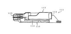
図11に示すような従来の光伝送モジュール111では、プリント基板112に光電変換モジュール113を設け、その光電変換モジュール113の一端に光ファイバケーブルコネクタ部114を設け、これをハウジング115に収納し、そのハウジング115の一端部に電気プラグ部116を設けている。この光伝送モジュール111は、光ファイバケーブルコネクタ部84に光ファイバケーブルを接続して使用される。 In a conventional optical transmission module 111 as shown in FIG. 11, a
しかしながら、従来の光伝送モジュール111は、大きさが等しい+、−の電気信号を光信号に変換し、光伝送路となる光ファイバケーブルに単に伝送あるいはこれとは逆の伝送を行うものである。 However, the conventional optical transmission module 111 converts electrical signals of + and − having the same size into optical signals and simply transmits them to an optical fiber cable serving as an optical transmission path, or performs the reverse transmission. .
つまり、従来の光伝送モジュール111は、1本の光ファイバについて見れば、送信あるいは受信動作しか行っていないため、特にサーバ用の高速インターフェース規格であるインフィニバンドで使用する場合に、モジュール全体が大型になる、部品が多い、高価であるといった問題がある。 In other words, since the conventional optical transmission module 111 performs only transmission or reception operation when viewed with respect to one optical fiber, the entire module is particularly large when used in InfiniBand, which is a high-speed interface standard for servers. There is a problem that there are many parts and is expensive.
特に、最近の光伝送モジュールには、1本の光ファイバで送信または受信を同時に行う双方向通信タイプが要求されてきているが、多芯は勿論のことながら単芯でも伝送速度を高速に保ちながらコンパクトにした製品はない。 In particular, recent optical transmission modules are required to have a two-way communication type in which transmission or reception is performed simultaneously using a single optical fiber. However, there is no compact product.
また、このような光伝送モジュールは、光ファイバが接続されたフェルールと光学部材とを光学的に結合する光学系接続構造を備えるものが一般的であるが、従来の光学系接続構造は、多芯を一括で接続することが難しいという問題がある。 Also, such an optical transmission module is generally provided with an optical system connection structure that optically couples a ferrule to which an optical fiber is connected and an optical member. There is a problem that it is difficult to connect the cores at once.
そこで、本発明の目的は、双方向通信タイプで多芯接続作業が簡単な光学系接続構造を提供することにある。 SUMMARY OF THE INVENTION An object of the present invention is to provide an optical system connection structure that is a bidirectional communication type and that allows easy multicore connection work.
また、本発明の他の目的は、小型で安価な光伝送モジュールを提供することにある。 Another object of the present invention is to provide a small and inexpensive optical transmission module.
本発明は上記目的を達成するために創案されたものであり、請求項1の発明は、フェルールに挿入された光ファイバと、上記光ファイバから出射する1つ以上の光信号L1及びその光信号L1とは波長の異なる上記光ファイバに入射する1つ以上の光信号L2の光路を変換する光学部材とを有する光学系接続構造において、
上記光学部材は上記光ファイバの光軸に対し傾斜した傾斜面を2面以上有し、上記傾斜面の1つに上記光信号L1を透過または反射させ上記光信号L2を反射または透過させる光フィルタを設け、
上記傾斜面の他の1つに上記光信号L1または上記光信号L2を反射させる反射面を形成し、
上記フェルールと対向する上記光学部材のファイバ側端面にファイバ用レンズを設けた光学系接続構造である。The present invention was devised to achieve the above object, and the invention of
The optical member has two or more inclined surfaces inclined with respect to the optical axis of the optical fiber, and transmits or reflects the optical signal L1 to one of the inclined surfaces to reflect or transmit the optical signal L2. Provided,
A reflective surface for reflecting the optical signal L1 or the optical signal L2 is formed on the other one of the inclined surfaces,
An optical system connection structure in which a fiber lens is provided on a fiber side end face of the optical member facing the ferrule.
請求項2の発明は、上記ファイバ用レンズは、上記光学部材のファイバ側端面に設けられた溝に形成される請求項1記載の光学系接続構造である。 A second aspect of the invention is the optical system connection structure according to the first aspect, wherein the fiber lens is formed in a groove provided on a fiber side end surface of the optical member.
請求項3の発明は、上記光ファイバは、単芯光ファイバを複数本並列に配置してなる多芯ファイバである請求項1または2記載の光学系接続構造である。 The invention according to
請求項4の発明は、上記光学部材に形成された上記傾斜面の1つに上記光フィルタを設け、その光フィルタを覆うように上記光信号L2に対して透明な樹脂を設けた請求項1〜3いずれかに記載の光学系接続構造である。 According to a fourth aspect of the present invention, the optical filter is provided on one of the inclined surfaces formed on the optical member, and a resin transparent to the optical signal L2 is provided so as to cover the optical filter. It is an optical system connection structure in any one of -3.
請求項5の発明は、フェルールに挿入された光ファイバから出射する1つ以上の光信号L1、及びその光信号L1とは波長の異なる上記光ファイバに入射する1つ以上の光信号L2の光路を変換する光学部材において、
上記フェルールと機械的に嵌合される嵌合部を有すると共に、上記光ファイバの光軸に対し傾斜した傾斜面を2面以上有し、
上記傾斜面の1つに上記複数の各光信号の一部またはほぼ全部を透過または反射させる光機能部材を設け、
上記傾斜面の他の1つに上記光信号を反射させる反射面を形成し、
上記フェルールと対向するファイバ側端面にファイバ用レンズを設けた光学部材である。According to a fifth aspect of the present invention, there is provided an optical path of one or more optical signals L1 emitted from an optical fiber inserted into a ferrule and one or more optical signals L2 incident on the optical fiber having a wavelength different from that of the optical signal L1. In an optical member that converts
Having a fitting part mechanically fitted to the ferrule, and having two or more inclined surfaces inclined with respect to the optical axis of the optical fiber,
An optical functional member that transmits or reflects part or all of the plurality of optical signals is provided on one of the inclined surfaces,
A reflecting surface for reflecting the optical signal is formed on the other one of the inclined surfaces;
An optical member in which a fiber lens is provided on a fiber-side end face facing the ferrule.
請求項6の発明は、複数の光信号を送信する送信用光素子アレイの配列ピッチに合わせて形成した複数個の送信用レンズからなる送信用レンズアレイ、及び複数の光信号を受信する受信用光素子アレイの配列ピッチに合わせて形成した複数個の受信用レンズからなる受信用レンズアレイを、上記送信用光素子アレイ及び上記受信用光素子アレイと対向するように上記光学部材の端面に形成した請求項5記載の光学部材である。 According to a sixth aspect of the present invention, there is provided a transmission lens array comprising a plurality of transmission lenses formed in accordance with an arrangement pitch of a transmission optical element array for transmitting a plurality of optical signals, and a reception for receiving a plurality of optical signals. A receiving lens array comprising a plurality of receiving lenses formed in accordance with the arrangement pitch of the optical element array is formed on the end face of the optical member so as to face the transmitting optical element array and the receiving optical element array. The optical member according to
請求項7の発明は、複数の光信号を送信する送信用光素子アレイと、複数の光信号を受信する受信用光素子アレイと、上記送信用光素子アレイから出射する送信光及び上記受信用光素子アレイで受光する受信光の光路を変換する光学部材とを有する光伝送モジュールにおいて、
パッケージ内に上記送信用光素子アレイと上記受信用光素子アレイを実装して光素子アセンブリを構成し、その光素子アセンブリを回路基板に接続し、その上方に、請求項1〜6いずれかに記載した光学系接続構造を設けた光伝送モジュールである。According to a seventh aspect of the present invention, there is provided a transmission optical element array for transmitting a plurality of optical signals, a reception optical element array for receiving a plurality of optical signals, transmission light emitted from the transmission optical element array, and the reception In an optical transmission module having an optical member that converts an optical path of received light received by the optical element array,
7. The optical element assembly for transmission and the optical element array for reception are mounted in a package to form an optical element assembly, the optical element assembly is connected to a circuit board, and thereabove, An optical transmission module provided with the described optical system connection structure.
請求項8の発明は、複数の光信号を送信する送信用光素子アレイと、複数の光信号を受信する受信用光素子アレイと、上記送信用光素子アレイから出射する送信光及び上記受信用光素子アレイで受光する受信光の光路を変換する光学部材とを有する光伝送モジュールにおいて、
パッケージ内に、上記送信用光素子アレイと、その送信用光素子アレイを駆動するドライバと、上記受信用光素子アレイと、その受信用光素子アレイの各出力を増幅する増幅器とを実装し、
上記パッケージを封止するためのガラス基板の裏面側に、上記送信用光素子アレイの配列ピッチに合わせて形成した複数個の送信用レンズからなる送信用レンズアレイと、上記受信用光素子アレイの配列ピッチに合わせて形成した複数個の受信用レンズからなる受信用レンズアレイとを配設し、
上記パッケージ内面と上記ガラス基板の裏面側が対向するように上記ガラス基板で封止し、そのガラス基板の表面に、請求項1〜5いずれかに記載した光学系接続構造を配設した光伝送モジュールである。The invention according to
In the package, the transmission optical element array, a driver for driving the transmission optical element array, the reception optical element array, and an amplifier that amplifies each output of the reception optical element array are mounted.
A transmitting lens array comprising a plurality of transmitting lenses formed on the back side of the glass substrate for sealing the package in accordance with the arrangement pitch of the transmitting optical element array, and the receiving optical element array. A receiving lens array comprising a plurality of receiving lenses formed in accordance with the arrangement pitch, and
An optical transmission module that is sealed with the glass substrate so that the inner surface of the package and the back side of the glass substrate face each other, and the optical system connection structure according to any one of
請求項9の発明は、上記パッケージの裏面にパッケージ用グランドを形成し、そのパッケージ用グランドと、上記回路基板に形成した基板用グランドとを電気的に接続した請求項7または8記載の光伝送モジュールである。 The invention according to
請求項10の発明は、上記光学部材と上記フェルールとを突き合わせて光学的に結合し、その上側からMTクリップを取り付けて上記光学部材と上記フェルールを一体固定し、上記MTクリップに、上記送信用光素子アレイから出射した光信号のうち、上記光フィルタあるいは上記光機能部材を透過した光信号の反射光が、上記送信用光素子アレイおよび上記受信用光素子アレイに入射するのを防止する反射光防止手段を設けた請求項7〜9いずれかに記載の光伝送モジュールである。 In the invention of
本発明によれば、組立作業が簡単な光学系接続構造を提供できる。 According to the present invention, it is possible to provide an optical system connection structure that can be easily assembled.
以下、本発明の好適な実施形態を添付図面にしたがって説明する。 DESCRIPTION OF EXEMPLARY EMBODIMENTS Hereinafter, preferred embodiments of the invention will be described with reference to the accompanying drawings.
まず、図1(a)で本発明の好適な実施形態を示す光伝送モジュールを用いた通信システムを説明する。 First, a communication system using an optical transmission module showing a preferred embodiment of the present invention will be described with reference to FIG.
図1(a)に示すように、通信システム100は、電気信号を光信号に、光信号を電気信号に変換する本実施形態に係る光伝送モジュール(多芯双方向光伝送モジュール、あるいはアクティブコネクタモジュール)10A,10B(以下、光伝送モジュール10ともいう)同士を、異なる波長の光信号を伝送するための光ファイバ2を複数本並列配置してなる多芯ファイバ3で接続し、電気信号を光信号に変換し、または光信号を電気信号にして光伝送モジュール10A,10B間で送信または受信するものである。 As shown in FIG. 1A, a
本実施形態では、光ファイバ2としてマルチモードファイバ(MMF)を用い、これを伝送12チャネル分として12本並列配置してなるテープファイバを多芯ファイバ3として用いた。各光ファイバ2を伝送する異なる波長の光信号としては、一方の光伝送モジュール10A用となる波長λ1の光信号L1と、他方の光伝送モジュール10B用となる波長λ2の光信号L2を用いた。後述する送信用光素子に用いる半導体レーザ(LD)として、波長が850nm近辺の光を出射する面発光レーザ(VCSEL)を用いることにより、波長λ1と波長λ2の波長間隔が±25nm(例えば、波長λ1:825nm、波長λ2:850nm)の光信号L1,L2を用いることができる。 In the present embodiment, a multimode fiber (MMF) is used as the
次に、光伝送モジュール10の全体構成を図6で説明する。 Next, the overall configuration of the
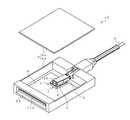
図6に示すように、光伝送モジュール10は、多芯ファイバ3と、フェルール4と、光学部材(光伝送モジュール用光学部材)5と、光素子としての送信用光素子および受信用光素子をセラミックス製のパッケージ6内に実装して封止した光素子アセンブリ7と、その光素子アセンブリ7に搭載された送信用光素子および受信用光素子が電気的に接続される回路基板(メイン基板)8と、他端部(図6では左斜め下端部)65が開口したモジュール用ケース9とで主に構成される。 As shown in FIG. 6, the
これらのうち、送信用光素子、受信用光素子、多芯ファイバ3、フェルール4、光学部材5との光学的な接続部分が本実施形態に係る光学系接続構造1である。 Among these, the optical connection part with the optical element for transmission, the optical element for reception, the
フェルール4には、多芯ファイバ3の他端部(図4では左端部)が挿入される。本実施形態では、フェルール4としてMT(Mechanically Transferable:多芯一括接続が可能)フェルールを用いた。 The other end (left end in FIG. 4) of the
光学部材5は、回路基板8の上方となる光素子アセンブリ7上に搭載され、送信用光素子からの光信号をフェルール4に挿入された光ファイバ2に入射、またはフェルール4に挿入された光ファイバ2からの光信号を受信用光素子に入射し、光素子アセンブリ7と光ファイバ2とを光学的に結合する。 The
すなわち、光学部材5は、光ファイバ2から出射する光信号L1及び光ファイバ2に入射する光信号L1とは波長の異なる光信号L2の光路を変換する。 That is, the
回路基板8の他端部は、その表裏面に図示しない複数個の接続端子が形成されて基板用カードエッジ部が構成される。この基板用カードエッジ部は、モジュール用ケース9の他端部に設けられる図示しないコネクタ部材の一端部に電気的に接続される。コネクタ部材の他端部は、その表裏面に複数個の接続端子が形成されてコネクタ用カードエッジ部(プラグ)11pが構成される。上述した装置、例えばメディアコンバータや高速コンピュータには、カードエッジ部11pと嵌合するアダプタが設けられており、上述した装置に光伝送モジュールが挿抜自在に設けられる。 The other end portion of the
モジュール用ケース9は、上部が開口した箱状の下ケース9dと、その開口を覆う板状の上ケース9uとからなり、放熱性が高いAlやZnなどの材料を用いて金属ダイカストで形成される。下ケース9dには、多芯ファイバ3の他端部、フェルール4、光学部材5、光素子アセンブリ7、回路基板8が収納される。下ケース9dには、ネジにより上ケース9uが取り付けられて固定される。 The
さて、本実施形態に係る光学系接続構造1と光学部材5を説明する。図1(b)は、本実施形態に係る光学系接続構造の主要部の概略上面の平面図、図1(c)はその縦断面図である。 Now, the optical
図1(b)および図1(c)に示すように、光学部材5のファイバ側には、多芯ファイバ3を構成する各光ファイバ2の他端面(図2に示すフェルール4の他端面)と対向する面(ファイバ側端面、あるいはファイバ側の光入出射端面)5fが形成されている。この光学部材5のファイバ側端面5fには、ファイバ側溝としての凹溝12fが形成され、その凹溝12fの凹部底面12cに、多芯ファイバ3の各光ファイバ2と光学的に結合され、その配列ピッチに合わせて形成した複数個のファイバ用レンズ13a,13b…からなるファイバ用レンズアレイ14fが形成される。 As shown in FIGS. 1B and 1C, on the fiber side of the
光学部材5の上部ほぼ中央には、光学部材5の一端面5f側に、光ファイバ2の光軸に対し略45°傾斜した2面以上の傾斜面の1つであるフィルタ搭載面15aを有するほぼ凹状(縦断面視でほぼ台形状)のフィルタ搭載部16が形成される。フィルタ搭載面15aには、フェルール4(図2参照)に挿入された光ファイバ2に入射する光信号L1を反射し、フェルール4に挿入された光ファイバ2から出射する光信号L2を透過させる光機能部材として、1枚の光フィルタ17が接着剤により貼り付けられて搭載される。 Near the center of the upper part of the
光フィルタ17は、所定波長帯域の光信号を反射し、それ以外の波長帯域の光信号を透過するものである。本実施形態では、光フィルタ17として、波長λ1の光信号L1を反射し、波長λ2の光信号L2を透過するように、誘電体多層膜からなる光フィルタを用いた。 The
光フィルタ17搭載後のフィルタ搭載部16には、光フィルタ17を覆うように、好ましくはフィルタ搭載部16を充填するように、ポッティングにより、光信号L1,L2に対して透明な樹脂rを設けるとよい。 The
この透明な樹脂rには、UV(紫外線)硬化型、熱硬化型を用いる。樹脂の材質はエポキシ系、アクリル系、シリコーン系等である。光フィルタ17を貼り付けるための上述した接着剤も同様の材質である。 As the transparent resin r, a UV (ultraviolet) curable type or a thermosetting type is used. The material of the resin is epoxy, acrylic or silicone. The adhesive described above for attaching the
光ファイバ2の光軸に対し略45°傾斜した2面以上の傾斜面として、他の1つである光学部材5の他端面(ファイバ側とは反対側(コネクタ部材側)の端面)5cには、フェルール4に挿入された光ファイバ2から出射され、光フィルタ17を透過した光信号L2を反射する反射面15rが形成される。 As two or more inclined surfaces inclined by approximately 45 ° with respect to the optical axis of the
反射面15rは、光学部材5とは屈折率が大きく異なる物質や、光学部材5よりも反射率が大きい物質と接することにより、光信号L2をほぼ全反射(95%以上反射)することができる。本実施形態では、光学部材5とは大きく異なる屈折率を有する物質として外気(空気)と接する構造となっているが、外気の他に、例えばAuなどの金属を蒸着した金属ミラーを用いても良い。 The reflective surface 15r can substantially totally reflect (reflect 95% or more) the optical signal L2 by contacting a material having a refractive index significantly different from that of the
パッケージ6は、上部に開口が形成され、その開口部に臨む内底面上に、光学部材5に入射する光信号L1を出射する送信用光素子(例えば、LD素子)を複数個並列配置してなる(例えば、配列ピッチ250μm)送信用光素子アレイ19と、光学部材5から出射する光信号L2が入射する受信用光素子(例えば、フォトダイオード(PD)素子)を複数個並列配置してなる(例えば、配列ピッチ250μm)受信用光素子アレイ20とが搭載される。 The
本実施形態では、多芯ファイバ3を構成する光ファイバ2の数に応じ、送信用光素子アレイ19として、12個のLD素子からなる面発光レーザアレイ(VCSELアレイ)を用い、受信用光素子アレイ20として、12個のPD素子からなるPDアレイを用いた。 In the present embodiment, a surface-emitting laser array (VCSEL array) composed of 12 LD elements is used as the transmitting
光学部材5の一端面5fとは異なる端面として、光学部材5の一端側の下面(光素子側端面、あるいは光素子側の入出射面)5dには、一方の光素子側溝としての凹溝12tが形成される。この凹溝12tの内上面には、送信用光素子アレイ19の配列ピッチに合わせて形成した複数個(本実施形態では12個)の送信用レンズからなる送信用レンズアレイ14tが形成される。 As an end surface different from the one end surface 5f of the
光学部材5の他端側の下面5dには、他方の光素子側溝としての凹溝12rが形成される。この凹溝12rの内上面には、受信用光素子アレイ20の配列ピッチに合わせて形成した複数個(本実施形態では12個)の受信用レンズからなる受信用レンズアレイ14rとが形成される。 On the lower surface 5d on the other end side of the
送信用レンズアレイ14tの各送信用レンズは、送信用光素子アレイ19のLD素子と対向するように、受信用レンズアレイ14rの各受信用レンズは、受信用光素子アレイ20の各PD素子と対向するように、光学部材5の下面5dにそれぞれ形成される。 Each receiving lens of the receiving
光学部材5では、凹溝12t,12rの内上面にレンズアレイを形成することで、例えば、製造組立工程において、光学部材5をトレイなどに並べて置いたときに、レンズ面がトレイに接触しないので、レンズ面の保護が可能になり、光学部材5の取り扱いが容易になる。 In the
この光学部材5は、プラスチック射出成形により、光信号L1,L2に対して透明な光学樹脂で一括形成される。材料に用いられる光学樹脂には、アクリル系樹脂、PC(ポリカーボネート)系樹脂、COP(シクロオレフィンポリマー)系樹脂などがある。また、材料強度や耐熱性を向上するのであれば、スーパーエンジニアリングプラスチックであるPEI(ポリエーテルイミド)が適している。本実施形態に係る光学部材5には、これらいずれの光学樹脂を用いてもよい。この際、光学部材5の材料である光学樹脂として、屈折率が1.45〜1.65のものを用いることができるが、光信号の損失が少なければこの屈折率に限る必要は無い。 The
ここで、光学系接続構造1を用いた光伝送モジュール10を、図2および図3(a)〜図3(c)を用いてより詳細に説明する。 Here, the
図2に示すように、パッケージ6の内底面上には、送信用光素子アレイ19の各LD素子を駆動するLDドライバアレイ21と、受信用光素子アレイ20の各PD素子から受信した電気信号を増幅するプリアンプとしてのTIA(トランスインピーダンス増幅器)アレイ22も搭載される。パッケージ6の上部には、パッケージ6内を封止するためのガラス基板23が取り付けられる。そして、ガラス基板23とパッケージ6は樹脂を用いて接合され、封止される。この際、パッケージ6の内面とガラス基板23の裏面側が対向するようにガラス基板23で封止する。 As shown in FIG. 2, on the inner bottom surface of the
ただし図2では、図1(b)および図1(c)の光学部材5の変形例である光学部材50を示した。この光学部材50は、送信用レンズアレイ14tと受信用レンズアレイ14rを光学部材50とは別体にしたものである。図2では、光学部材50の他端部に反射面15rを形成した例を示した。 However, in FIG. 2, the
この光学部材50を用いる場合には、送信用光素子アレイ19と受信用光素子アレイ20の直上となるガラス基板23の下面(裏面)に、送信用レンズアレイ14tと受信用レンズアレイ14rが一体形成された光素子側レンズアレイ24を設ける。光素子側レンズアレイ24も光学部材50と同じ材料を用いて、プラスチック射出成形により一括形成される。 When this
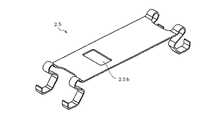
光学部材50の一端面5fとフェルール4の他端面(フェルール側の光入出射面)4cは、それぞれ高さ方向(図2の上下方向)が光ファイバ2の光軸の法線方向と平行になるように平面に形成される。これら光学部材50の一端面5fとフェルール4の他端面4cは突き合わされて光学的に結合され、この状態で上側から取り付けられるMTクリップ25により、光学部材50の他端面5cとフェルール4の一端面4fの両側から押さえられることで、光学部材50とフェルール4が一体固定される。 The one end face 5f of the
MTクリップ25には、フィルタ搭載部16の上方に位置する領域に、図7に示すような反射光防止手段としての開口部25hを形成すると良い。ここでいう反射光防止手段とは、送信用光素子アレイ19から出射した光信号のうち、光フィルタ17を透過した光信号の反射光(戻り光)が、送信用光素子アレイ19および光受信用光素子アレイ20に入射するのを防止するものである。 In the
送信用光素子アレイ19から出射した波長λ1の光信号光は、光フィルタ17によってほとんど(95%以上)が反射されるが、光フィルタ17で反射せずに透過した僅かな光量の光信号光は、MTクリップ25で反射されて再び光フィルタ17に戻る。再び光フィルタ17に戻った波長λ1の戻り光は、開口部25hがない場合、ほとんどは(95%以上)光フィルタ17により反射されて受信用光素子アレイ20に入射し、残りの僅かな戻り光は光フィルタ17を透過し送信用光素子アレイ19に戻る。受信用光素子アレイ20に入射した波長λ1の戻り光は、受信用光素子アレイ20が本来受信する波長λ2の光信号L2に対してノイズとなる。また、送信用光素子アレイ19に戻った戻り光は、送信用光素子アレイ19の発振動作を不安定にする。従って、戻り光は信号品質を低下させるので好ましくない。 The optical signal light having the
そこで、図7に示すように、MTクリップ25に開口部25hを設けることにより、光フィルタ17を反射せずに透過した僅かな光量の波長λ1の光信号光を光伝送モジュール10(図2参照)の外部に放出することができるため、送信用光素子アレイ19および光受信用光素子アレイ20の動作を安定化することができる。なお、光フィルタ17の性能によっては(例えば99%以上反射するとき)、MTクリップ25に開口部25hを設けなくてもよい。 Therefore, as shown in FIG. 7, by providing an
また、図7のMTクリップ25の変形例として、図9に示すようなMTクリップ95を用いてもよい。このMTクリップ95では、フィルタ搭載部16の上方に位置する領域に、反射光防止手段としての傾斜部96を設けた。ここでは、MTクリップ25の平坦な部分に、側面視で略台形状の凹部を形成し、その凹部の他端側の傾斜した部分を傾斜部96としたMTクリップ95を用いた。 Further, as a modification of the
MTクリップ95を用いた光伝送モジュール90では、送信用光素子アレイ19から出射して光フィルタ17を透過した光信号は、傾斜部96で反射されても別の光路に反射され、元の光路を戻ることがないため、送信用光素子アレイ19および受信用光素子アレイ20の動作を安定化することができる。 In the
図2に示すように、セラミックスからなるパッケージ6に、送信用光素子アレイ19、受信用光素子アレイ20、LDドライバアレイ21、TIAアレイ22を収納して実装し、ガラス基板23の下面に光素子側レンズアレイ24を接着剤で貼り付ける。次に、パッケージ6内に光素子レンズアレイ24が実装されるように、パッケージ6にガラス基板23を載せ、パッケージ6とガラス基板23とを樹脂を用いて封止して、光素子アセンブリ7が得られる。光素子アセンブリ7の外径は、約1cm×1cmである。この光素子アセンブリ7と光学部材50とで光送受信アセンブリ(OSA)が構成される。 As shown in FIG. 2, a transmitting
次に、図3(a)および図3(b)に示すように、パッケージ6の下面(裏面)には、回路基板8上に光素子アセンブリ7を搭載するための半田ボール31が複数個格子状に並べて取り付けられる。つまり、パッケージ6はBGA(Ball Grid Array)はんだを構成する。この複数個の半田ボール31の一部をパッケージ用グランドとし、そのパッケージ用グランドと、回路基板8上に形成した基板用グランドとを電気的に接続する。 Next, as shown in FIGS. 3A and 3B, a plurality of
図2において、回路基板8に光素子アセンブリ7を取り付け接続する方法としては、BGAはんだを用いる方法以外に、パッケージ6の下面と回路基板8とを導電性接着剤で接着する方法もある。 In FIG. 2, as a method of attaching and connecting the
パッケージ6の下面と回路基板8とを導電性接着剤で接着する場合には、パッケージ6と回路基板8との間で各チャンネルの信号を電気的に伝送するために、パッケージ6と回路基板8との間の各チャンネルをワイヤボンディングによって電気的に接続する。従って、パッケージ6の一部にはワイヤボンディングするための領域(図示せず)が形成されている。 When the lower surface of the
更に、パッケージ6が上方に位置する回路基板8の光素子モジュール搭載部7eには、パッケージ6の下面の一部を露出させる放熱用の貫通穴26が設けられる。 Further, a heat dissipation through
貫通孔26には熱伝導部材を充填または配設して放熱効果を高めると良い。熱伝導部材としてはシリコーン樹脂から成る熱伝導シート、またはカーボン材でも良く、あるいは熱伝導性の良い金属部材でも良い。 The through
次に、フェルール4を図4で、光学部材50を図5でより詳細に説明する。 Next, the
図4に示すように、フェルール4は、全体がほぼ直方体状に形成され、その他端面4cの両側には、光学部材50と機械的に嵌合するための被嵌合部として、フェルール用嵌合溝41,41が形成される。これらフェルール用嵌合溝41,41間には、他端面4cから一端面4fまでフェルール4の長さ方向に沿って貫通したファイバ挿入孔42が複数個(図4では12個)並列配置して形成される。各ファイバ挿入孔42は、上述したファイバ用レンズアレイ14fの各ファイバ用レンズ13a,13b…にそれぞれ対向するように、各ファイバ用レンズ13a,13b…と同じ配列ピッチで形成される。 As shown in FIG. 4, the
図2に示すように、ファイバ挿入孔42は、フェルール4の一端部に形成されて被覆除去されない多芯ファイバ3が収納される大径収納部42fと、フェルール4の他端部に形成されて被覆除去された各光ファイバ2がそれぞれ収納される小径収納部42cとからなる。 As shown in FIG. 2, the
フェルール4に多芯ファイバ3を取り付けるには、まず、多芯ファイバ3の一部の被覆を除去し、各光ファイバ2を解いた後、それぞれの他端面を直角カットして直角カット面を形成する。その後、各光ファイバ2のそれぞれの直角カット面が、フェルール4の他端面4cと略一致するまで、ファイバ挿入孔42に多芯ファイバ3を挿入してフェルール4に樹脂を用いて固定する。なお、各光ファイバ2は、フェルール4の他端面4cから若干(0.2mm程度)突出または若干フェルール4の内部に引き込んでいても良い。 To attach the
すなわち、フェルール4の他端面4cから突出した各光ファイバ2の長さは、図1(c)に示すファイバ用レンズアレイ14fに当たらず、更にファイバ用レンズアレイ14fとの光結合損失が所望の範囲内であれば良い。また、フェルール4の他端面4cからフェルール4の内部に引き込んだ各光ファイバ2の端面までの長さは、ファイバ用レンズアレイ14fとの光結合損失が所望の範囲内であれば良い。 That is, the length of each
各光ファイバ2を解いた後、それぞれの他端部をファイバ挿入孔42に挿通し、フェルール4の他端面4cに一致するように、ファイバ挿入孔42から突出した各光ファイバ2の他端部を直角カットして直角カット面を形成してもよい。 After unraveling each
図5に示すように、光学部材50は、外形がフェルール4とほぼ同形状に形成され、その一端面5fには、フェルール用嵌合溝41,41(図4参照)と機械的に嵌合する嵌合部としての嵌合突起51,51が形成される。 As shown in FIG. 5, the
嵌合突起51,51とフェルール用嵌合溝41,41とで互いに嵌合する結合部(接続部)が構成され、これら嵌合突起51,51とフェルール用嵌合溝41,41とを嵌合することで、光学部材50の一端面5fとフェルール4の他端面4cが突き合わせ接続されて各光ファイバ2と光学部材50が光学的に結合される。 The
もちろん、光学部材側に嵌合部としての嵌合溝を形成し、フェルール側に被嵌合部としての嵌合突起を形成してもよい。 Of course, a fitting groove as a fitting portion may be formed on the optical member side, and a fitting protrusion as a fitted portion may be formed on the ferrule side.
光学部材50の上縁部は、光部品あるいは電気部品を実装する実装装置(マウンタ)のコレットチャックでつかむために、四角枠状の平坦部50fになっている。 The upper edge portion of the
次に、本実施形態の作用を説明する。 Next, the operation of this embodiment will be described.
図2に示す光伝送モジュール10では、回路基板8からの各チャネル用となる12個の電気信号は、送信用光素子アレイ19で波長λ1の光信号L1にそれぞれ変換され、各光信号L1が光素子側レンズアレイ24の送信用レンズアレイ14tでコリメート光に変換され(光学部材5の場合は、その送信用レンズアレイ14tでコリメート光に変換され)、光学部材50に入射される。その後、各光信号L1は、光フィルタ17で反射され、ファイバ用レンズアレイ14fで集光されて光学部材50から出射され、多芯ファイバ3の各光ファイバ2に入射されることで、相手側の光伝送モジュールに送信される。 In the
また、相手側の光伝送モジュールから送信された各チャネル用の12個の波長λ2の光信号L2は、多芯ファイバ3の各光ファイバ2から出射され、光学部材50のファイバ用レンズアレイ14fでコリメート光に変換されて光学部材50に入射され、光フィルタ17を透過し、反射面15rで反射されて光学部材50から出射される。その後、各光信号L2は、光素子側レンズアレイ24の受信用レンズアレイ14rで集光され、次に受信用光素子アレイ20で各チャネル用の12個の電気信号に変換され、回路基板8に伝送されることで、相手側の光伝送モジュールからの各光信号L2が受信される。 Also, the twelve optical signals L2 of wavelength λ2 transmitted from the counterpart optical transmission module are emitted from the
光学系接続構造1は、フェルール4と光学部材50の光入出射面4c,5fを平面にしており、その光入出射面4c,5fに形成した嵌合部によりフェルール4と光学部材50とを突き合わせ接続して、各光ファイバ2と光学部材50とを光学的に結合している。 In the optical
さらに、光学系接続構造1は、フェルール4に挿入される光ファイバ2として光学的接続が簡単なMMFを用いており、しかも光学部材50の凹溝12fにファイバ用レンズアレイ14fを形成している。 Further, the optical
これにより、光学系接続構造1では、ファイバ用レンズ14fを出射した光信号L1,L2を空間となる凹溝12fを介して伝送し、各光ファイバ2とレンズ結合させる構造であるため、各光ファイバ2の他端面を直角カットだけすればよく、PC(物理的接触)研磨のような複雑で面倒な端面処理が不要であり、組立作業が簡単である。 Thereby, in the optical
また、光学系接続構造1は、送信用光素子アレイ19として光ファイバ2などの端面反射などによる戻り光に強いVCSELアレイを用いており、この点でも複雑で面倒な端面処理が不要であり、組立作業が簡単である。 In addition, the optical
これにより、光学系接続構造1を用いれば、1本の光ファイバ2で双方向の同時光通信を行うタイプの光伝送モジュールに限らず、これを多芯化した伝送速度が高速の光伝送モジュール10の組み立ても簡単になる。 Thus, if the optical
この光学系接続構造1を備えた光伝送モジュール10は、波長λ1,λ2の光信号L1,L2を1セットとして、これらを1本の光ファイバ2で送信または受信するために、多芯ファイバ3を用いており、その多芯ファイバ3からの光信号L1,L2を一括して多芯双方向通信するために光学部材50を備えている。 The
この光学部材50にファイバ用レンズ14f、フィルタ搭載部16、反射面15rを形成し、フィルタ搭載部16に1枚の光フィルタ17を搭載するだけで光伝送モジュール10の主要部を構成できるため、従来の光伝送モジュールに比べて構成が簡単である。しかも双方向通信が可能となるため、一方向通信と比較して光ファイバ2の芯数を1/2にでき、小型で安価な光伝送モジュールを実現できる。 Since the
更に、光素子アセンブリ7のガラス基板23の裏面に光素子側レンズアレイ24を設け、光学部材50と、焦点距離が短いマイクロレンズアレイである送信用レンズアレイ14tおよび受信用レンズアレイ14rとを別体にすることで、光軸ズレを緩和することができるため、光伝送モジュール10をより低損失で高信頼性なものにできる。 Further, an optical element
ここで、樹脂材から構成される光学部材5の熱膨張は大きく(熱膨張係数が60ppm/℃)、セラミックスから構成されるパッケージ6は熱膨張が小さい(熱膨張係数が7ppm/℃)。 Here, the thermal expansion of the
更に、図1(c)に示した光学部材5と送信用レンズアレイ14tおよび受信用レンズアレイ14rが一体となった構造では、光学部材5をパッケージ6に実装する際、光学部材5の一部がパッケージ6の上縁と接続固定される構造となる(図8参照)。 Furthermore, in the structure in which the
このため、温度変化によって光学部材5が熱膨張した場合、熱膨張の小さなパッケージ6で熱膨張の大きな光学部材5の熱膨張を抑えようとしても、光学部材5の一部がパッケージ6に接続固定される構造では、光学部材5の熱膨張を抑える効果は小さい。 For this reason, when the
これに対し、図2に示すように、光学部材50と送信用レンズアレイ14tおよび受信用レンズアレイ14rが別体となった構造では、光素子側レンズアレイ24のレンズ面とは反対側の面の全面を、熱膨張が小さい(熱膨張係数が7ppm/℃)ガラス基板23と接着固定している。 On the other hand, as shown in FIG. 2, in the structure in which the
これにより、光伝送モジュール10では、光素子側レンズアレイ24全体がガラス基板23と強固に接着固定されているため、光素子側レンズアレイ24が熱により膨張しようとしても、熱膨張が小さいガラス基板23によって光素子側レンズアレイ24の熱膨張を抑制することができる。 Thereby, in the
この光伝送モジュール10では、送信用光素子アレイ19及び受信用光素子アレイ20を実装したパッケージ6の上縁とガラス基板23とを樹脂で封止するため、樹脂が外気に触れる面積が極めて少ない。このため、パッケージ6内に外気から水分が浸入することを低減できるので、パッケージ6内の光素子や電子デバイスの信頼性をより高めることができる。 In this
また、光伝送モジュール10は、フィルタ搭載部16に光フィルタ17を搭載し、その光フィルタ17を覆うように光信号L1,L2に対して透明な樹脂rを設けているため、フィルタ搭載面15aと光フィルタ17の接合部を補強すると共に、空気中の湿気などによる光フィルタ17の劣化などを抑制することができ、光フィルタ17裏面からの光信号L2の不要な反射も防止できる。 Further, since the
更に、フィルタ搭載面15aと対向する面15wを光ファイバ2の光軸に対して直交する方向から傾斜させることにより、フィルタ搭載部16に充填した樹脂rがフィルタ搭載面15aと対向する面15wから剥離した場合でも、フィルタ搭載面15aと対向する面15wからの反射戻り光を低減することができる。 Further, by inclining the surface 15w facing the filter mounting surface 15a from the direction perpendicular to the optical axis of the
光学部材50の上縁部は、平坦部50fになっている。一般的なコレットチャックの断面は逆漏斗状(断面視で三角形状)になっていたり、下面が平坦状になっている。このため、光学部材50の上縁部が平坦部50fなので、光学部材50に上方から実装装置のコレットチャックを近づけ、空気吸引すれば、コレットチャックで光学部材50を簡単につかんで実装できる。 The upper edge portion of the
上記実施形態では、送信用レンズアレイ14tと受信用レンズアレイ14rを光学部材50とは別体に構成し、光学部材50を用いた光伝送モジュール10を説明したが、送信用レンズアレイ14tと受信用レンズアレイ14rを一体に構成した図1(c)の光学部材5を用いて、図8に示すような光伝送モジュール80としてもよい。 In the above embodiment, the
光伝送モジュール80では、光学部材5の平坦な下面の周縁と、パッケージ6の上縁とを樹脂を用いて接合し、樹脂封止した光素子アセンブリ77とする。 In the
上記実施形態では、光フィルタ17として、波長λ1の光信号L1を反射、波長λ2の光信号L2を透過するものを使用したが、波長λ1の光信号L1を透過、波長λ2の光信号L2を反射する光フィルタを用いてもよい。この場合、光学部材5,50の構造を変更することなく、送信用光素子アレイ19、受信用光素子アレイ20の配置を入れ替えればよい。 In the above embodiment, the
ここで、図1(a)に示す通信システム100では、光伝送モジュール10Aが図1(c)に示すように、光フィルタ17として、波長λ1の光信号L1を反射、波長λ2の光信号L2を透過する構成である場合、光伝送モジュール10Bは、光フィルタ17として、波長λ1の光信号L1を透過し、波長λ2の光信号L2を反射する構成にし、送信用光素子アレイ19が波長λ2の光信号を出射し、受信用光素子アレイ20が波長λ1の光信号を受光する構成とすると良い。 Here, in the
このように光学部材5に対して、送信用光素子および受信用光素子の配置を変えずに、光フィルタの透過または反射する波長特性を変えた光伝送モジュール10A,10Bを通信ペアとして用いた構成とすることにより、光伝送モジュール10A,10Bを駆動する回路系の構成が共通となり、システムの構築が容易となる。 In this way, the
また、上記実施形態では、波長λ1,λ2の光信号L1,L2を多芯双方向通信する例で説明したが、波長が異なる3波以上の光信号を用いてもよい。この場合、光フィルタは複数枚必要になるため、これに応じて光学部材5,50の構成も適宜変更すればよい。 In the above-described embodiment, the optical signals L1 and L2 having the wavelengths λ1 and λ2 have been described as examples of multicore bidirectional communication. However, three or more optical signals having different wavelengths may be used. In this case, since a plurality of optical filters are required, the configuration of the
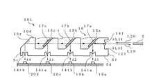
例えば、図1の光学系接続構造1の変形例である図10に示す光学系接続構造101のように、光ファイバ2の長手方向に沿って光学部材105を長尺に形成し、その4個の傾斜面のうちの3個をファイバ側から順にフィルタ搭載面15a〜15cとすると共に、残る傾斜面の1個を反射面15rとし、下面5dに形成した4個の各凹溝に対応させて、2個の送信用レンズアレイ14ta,14tbと、2個の受信用レンズアレイ14ra,14rbを設けてもよい。 For example, as shown in an optical
フィルタ搭載部15aには、波長λ1の光信号を反射し、それ以外の波長の光信号を透過する光フィルタ17aを、フィルタ搭載部15bには、波長λ2の光信号を反射し、それ以外の波長の光信号を透過する光フィルタ17bを、フィルタ搭載部15cには、波長λ3の光信号を反射し、それ以外の波長の光信号を透過する光フィルタ17cを搭載する。 The filter mounting portion 15a reflects an optical signal 17a that reflects an optical signal having a wavelength λ1 and transmits an optical signal having a wavelength other than that. The
光学部材105の下方には、ファイバ側から順に、波長λ1の光信号を出射する送信用光素子アレイ19a、波長λ2の光信号を出射する送信用光素子アレイ19b、受信用光素子アレイ20c,20dをそれぞれ設ける。 Below the
この光学系接続構造101は、モジュール間の伝送に、互いに異なる4つの波長(λ1〜λ4)の光信号を用いた例である。光学系接続構造101では、送信は、送信用光素子アレイ19a,19bで出射した波長λ1,λ2の光信号を波長多重し、波長多重光信号L10(上述した光信号L1に相当)を各光ファイバ2に入射させる。また、受信は、各光ファイバ2から出射された波長λ3+λ4の波長多重光信号L20(上述した光信号L2に相当)を波長分離し、受信用光素子アレイ20c,20dで受光させる。 This optical
光学系接続構造101によれば、図1の光学接続構造1に比べ、光信号のトータル伝送速度をさらに高速にできる。 According to the optical
図1(c)の実施形態では、光機能部材として、波長により光信号を透過または反射させる光フィルタ17を用いたが、光フィルタ17に代えてハーフミラーを用いることもできる。ハーフミラーは波長に応じて分波・合波する波長選択機能は有しないが、所定の波長の光信号の透過率または反射率を任意に設定することができる。 In the embodiment of FIG. 1C, the
ハーフミラーを用いた光学部材は、図1(c)の光学部材5において、光フィルタ17をハーフミラーに置き換える点を除いて同じ構成である。このため、便宜上図1(c)を用いて、その機能を説明する。 The optical member using the half mirror has the same configuration except that the
送信用光素子アレイ19を出射した波長λ1の光信号L1は、ハーフミラーでX%が反射されてファイバ用レンズアレイ14fにより各光ファイバ2に光結合して各光ファイバ2内を伝搬し、相手方の光伝送モジュールに送信される。 The optical signal L1 of wavelength λ1 emitted from the transmitting
なお、ハーフミラーで反射されずに透過した(100−X)%の光信号は、ハーフミラーの上方に設けられたモニタ用受光素子(図示せず)によって光信号L1の光量をモニタすることにより、送信用光素子アレイ19の発光制御をすることができる。 The (100-X)% optical signal transmitted without being reflected by the half mirror is monitored by monitoring the light quantity of the optical signal L1 by a monitoring light receiving element (not shown) provided above the half mirror. The light emission of the transmitting
次に、相手方の光伝送モジュールから送信された波長λ1の光信号L1は、ハーフミラーで(100−X)%が透過し、反射面15rによってほぼ全反射されて受信用光素子アレイ20に入射して受信される。 Next, the optical signal L1 having the wavelength λ1 transmitted from the counterpart optical transmission module transmits (100-X)% by the half mirror, is almost totally reflected by the reflecting surface 15r, and enters the receiving
なお、ハーフミラーで透過せずに反射した相手方の光伝送モジュールから送信された波長λ1の光信号L1は、送信用光素子アレイ19に入射してしまう。従って、Xを10%程度にし、送信用光素子アレイ19に入射する光量を少なくする必要がある。しかし、送信用光素子アレイ19から送信された光信号が相手方の光伝送モジュールの受信用光素子アレイ20に入射までの伝送率はX×(100−X)%の式で表せることから、Xを10%にすると光信号L1の伝送率は約9%であり、波長フィルタを使用した場合の約100%(より正確には、約95×約95%=90%以上)に比べて損失が大きくなる。 The optical signal L1 having the wavelength λ1 transmitted from the counterpart optical transmission module reflected without being transmitted through the half mirror is incident on the transmitting
しかし、本実施形態に係る光伝送モジュールは、送信側と受信側が各光ファイバ2を介して一体の構造であり、任意の相手側光伝送モジュールと接続するための光コネクタ開口部を有する従来の光伝送モジュールとは異なり、厳密な光出力の調整や制限が無く、エラーが無く通信できる範囲であれば、損失が大きくても光の出力レベルを光伝送モジュール製造者が自由に設定できる。 However, the optical transmission module according to this embodiment has a conventional structure in which the transmission side and the reception side are integrated with each other through the
なお、相手方の光伝送モジュールが波長λ1の光信号L1を送信するときは、送信用光素子アレイ19を動作停止状態、または待機状態にしておいても良い。 When the counterpart optical transmission module transmits the optical signal L1 having the wavelength λ1, the transmitting
また、ハーフミラーを備えた光伝送モジュールを用いた通信システムは、相手方の光伝送モジュールも同じ波長λ1の光信号のみを用いる点が、図1(a)の通信システム100と相違し、その他の動作は同じである。 The communication system using the optical transmission module provided with the half mirror is different from the
なお、上記したように、同じ波長λ1を用いた通信システムでは、相手方の光伝送モジュールが波長λ1の光信号L1を送信するときは、光信号L1の衝突が生じないように自身の送信用光素子アレイ19を動作停止状態、または待機状態にしておく。 As described above, in the communication system using the same wavelength λ1, when the counterpart optical transmission module transmits the optical signal L1 having the wavelength λ1, its own transmission light is used so that the optical signal L1 does not collide. The
1 光学系接続構造
2 光ファイバ
3 多芯ファイバ
4 フェルール
5 光学部材
10 光伝送モジュール
15a フィルタ搭載面(傾斜面の1つ)
15r 反射面(傾斜面の他の1つ)
17 光フィルタ
L1 波長λ1の光信号
L2 波長λ2の光信号DESCRIPTION OF
15r reflective surface (other one of inclined surfaces)
17 Optical filter L1 Optical signal L2 with wavelength λ1 Optical signal L2 with wavelength λ2
Claims (10)
Translated fromJapanese上記光学部材は上記光ファイバの光軸に対し傾斜した傾斜面を2面以上有し、上記傾斜面の1つに上記光信号L1を透過または反射させ上記光信号L2を反射または透過させる光フィルタを設け、
上記傾斜面の他の1つに上記光信号L1または上記光信号L2を反射させる反射面を形成し、
上記フェルールと対向する上記光学部材のファイバ側端面にファイバ用レンズを設けたことを特徴とする光学系接続構造。The optical fiber inserted into the ferrule, one or more optical signals L1 emitted from the optical fiber, and one or more optical signals L2 incident on the optical fiber having a wavelength different from that of the optical signal L1 are converted. In an optical system connection structure having an optical member,
The optical member has two or more inclined surfaces inclined with respect to the optical axis of the optical fiber, and transmits or reflects the optical signal L1 to one of the inclined surfaces to reflect or transmit the optical signal L2. Provided,
A reflective surface for reflecting the optical signal L1 or the optical signal L2 is formed on the other one of the inclined surfaces,
An optical system connection structure, wherein a fiber lens is provided on a fiber side end face of the optical member facing the ferrule.
上記フェルールと機械的に嵌合される嵌合部を有すると共に、上記光ファイバの光軸に対し傾斜した傾斜面を2面以上有し、
上記傾斜面の1つに上記複数の各光信号の一部またはほぼ全部を透過または反射させる光機能部材を設け、
上記傾斜面の他の1つに上記光信号を反射させる反射面を形成し、
上記フェルールと対向するファイバ側端面にファイバ用レンズを設けたことを特徴とする光学部材。In an optical member that converts one or more optical signals L1 emitted from an optical fiber inserted into a ferrule, and one or more optical signals L2 incident on the optical fiber having a wavelength different from that of the optical signal L1,
Having a fitting part mechanically fitted to the ferrule, and having two or more inclined surfaces inclined with respect to the optical axis of the optical fiber,
One of the inclined surfaces is provided with an optical functional member that transmits or reflects part or almost all of the plurality of optical signals,
A reflecting surface for reflecting the optical signal is formed on the other one of the inclined surfaces;
An optical member, wherein a fiber lens is provided on a fiber-side end face facing the ferrule.
パッケージ内に上記送信用光素子アレイと上記受信用光素子アレイを実装して光素子アセンブリを構成し、その光素子アセンブリを回路基板に接続し、その上方に、請求項1〜6いずれかに記載した光学系接続構造を設けたことを特徴とする光伝送モジュール。Transmitting optical element array for transmitting a plurality of optical signals, receiving optical element array for receiving a plurality of optical signals, transmission light emitted from the transmitting optical element array, and reception received by the receiving optical element array In an optical transmission module having an optical member that converts an optical path of light,
7. The optical element assembly for transmission and the optical element array for reception are mounted in a package to form an optical element assembly, the optical element assembly is connected to a circuit board, and thereabove, An optical transmission module comprising the described optical system connection structure.
パッケージ内に、上記送信用光素子アレイと、その送信用光素子アレイを駆動するドライバと、上記受信用光素子アレイと、その受信用光素子アレイの各出力を増幅する増幅器とを実装し、
上記パッケージを封止するためのガラス基板の裏面側に、上記送信用光素子アレイの配列ピッチに合わせて形成した複数個の送信用レンズからなる送信用レンズアレイと、上記受信用光素子アレイの配列ピッチに合わせて形成した複数個の受信用レンズからなる受信用レンズアレイとを配設し、
上記パッケージ内面と上記ガラス基板の裏面側が対向するように上記ガラス基板で封止し、そのガラス基板の表面に、請求項1〜5いずれかに記載した光学系接続構造を配設したことを特徴とする光伝送モジュール。Transmitting optical element array for transmitting a plurality of optical signals, receiving optical element array for receiving a plurality of optical signals, transmission light emitted from the transmitting optical element array, and reception received by the receiving optical element array In an optical transmission module having an optical member that converts an optical path of light,
In the package, the transmission optical element array, a driver for driving the transmission optical element array, the reception optical element array, and an amplifier that amplifies each output of the reception optical element array are mounted.
A transmitting lens array comprising a plurality of transmitting lenses formed on the back side of the glass substrate for sealing the package in accordance with the arrangement pitch of the transmitting optical element array, and the receiving optical element array. A receiving lens array comprising a plurality of receiving lenses formed in accordance with the arrangement pitch, and
It is sealed with the glass substrate so that the inner surface of the package and the back surface side of the glass substrate face each other, and the optical system connection structure according to any one of claims 1 to 5 is disposed on the surface of the glass substrate. An optical transmission module.
Priority Applications (3)
| Application Number | Priority Date | Filing Date | Title |
|---|---|---|---|
| JP2007066922AJP2008225339A (en) | 2007-03-15 | 2007-03-15 | Optical system connection structure, optical member, and optical transmission module |
| US12/010,078US7539367B2 (en) | 2007-03-15 | 2008-01-18 | Optical system connection structure, optical component, and optical communication module |
| CN2008100860549ACN101266325B (en) | 2007-03-15 | 2008-03-14 | Optical system connection structure, optical component, and optical communication module |
Applications Claiming Priority (1)
| Application Number | Priority Date | Filing Date | Title |
|---|---|---|---|
| JP2007066922AJP2008225339A (en) | 2007-03-15 | 2007-03-15 | Optical system connection structure, optical member, and optical transmission module |
Publications (1)
| Publication Number | Publication Date |
|---|---|
| JP2008225339Atrue JP2008225339A (en) | 2008-09-25 |
Family
ID=39762784
Family Applications (1)
| Application Number | Title | Priority Date | Filing Date |
|---|---|---|---|
| JP2007066922APendingJP2008225339A (en) | 2007-03-15 | 2007-03-15 | Optical system connection structure, optical member, and optical transmission module |
Country Status (3)
| Country | Link |
|---|---|
| US (1) | US7539367B2 (en) |
| JP (1) | JP2008225339A (en) |
| CN (1) | CN101266325B (en) |
Cited By (12)
| Publication number | Priority date | Publication date | Assignee | Title |
|---|---|---|---|---|
| WO2010098395A1 (en) | 2009-02-25 | 2010-09-02 | 矢崎総業株式会社 | Optical communication module and optical communication connector |
| WO2011077723A1 (en)* | 2009-12-22 | 2011-06-30 | 株式会社エンプラス | Lens array and optical module provided therewith |
| JP2012018363A (en)* | 2010-07-09 | 2012-01-26 | Enplas Corp | Lens array and optical module comprising the same |
| JP2012123250A (en)* | 2010-12-09 | 2012-06-28 | Enplas Corp | Lens array and manufacturing method of the same |
| JP2012194372A (en)* | 2011-03-16 | 2012-10-11 | Enplas Corp | Lens array and optical module equipped with the same |
| JP2014092716A (en)* | 2012-11-05 | 2014-05-19 | Sumitomo Electric Ind Ltd | Clip member and optical module including the same |
| JP2015025991A (en)* | 2013-07-29 | 2015-02-05 | 住友電気工業株式会社 | Lens component and optical module |
| JP2015099307A (en)* | 2013-11-20 | 2015-05-28 | 日立金属株式会社 | Optical communication module and optical block for use in the same |
| JP2015108646A (en)* | 2013-12-03 | 2015-06-11 | 住友電気工業株式会社 | Optical receiver module |
| KR20190123066A (en)* | 2018-04-23 | 2019-10-31 | 주식회사 옵토웰 | Coarse wavelength division multiplexing optical subassembly moudle |
| JP2020038250A (en)* | 2018-09-03 | 2020-03-12 | 株式会社エンプラス | Optical module |
| JP2024543632A (en)* | 2021-12-09 | 2024-11-21 | 華為技術有限公司 | Optical Modules, Ferrules, and Fiber Optic Connectors |
Families Citing this family (151)
| Publication number | Priority date | Publication date | Assignee | Title |
|---|---|---|---|---|
| US9341828B2 (en) | 2011-03-31 | 2016-05-17 | Globalfoundries Inc. | Multi-core fiber optical coupling elements |
| JP5157393B2 (en)* | 2007-11-29 | 2013-03-06 | 住友電気工業株式会社 | Optical module and cable unit with optical module |
| JP4914819B2 (en)* | 2007-12-14 | 2012-04-11 | 株式会社エンプラス | Optical coupling element and optical module having the same |
| JP5428256B2 (en)* | 2008-09-10 | 2014-02-26 | 日本電気株式会社 | Optical module and optical transmission method |
| US8412050B2 (en)* | 2008-10-23 | 2013-04-02 | Alcatel Lucent | Coaxial free space optical telescope and systems using the same |
| US8335411B2 (en)* | 2008-11-11 | 2012-12-18 | Ultra Communications, Inc. | Fiber optic bi-directional coupling lens |
| US8985865B2 (en)* | 2008-11-28 | 2015-03-24 | Us Conec, Ltd. | Unitary fiber optic ferrule and adapter therefor |
| EP2359172B1 (en) | 2008-12-22 | 2015-02-25 | Panasonic Corporation | Method for forming mirror-reflecting film in optical wiring board |
| JP5446565B2 (en)* | 2009-08-07 | 2014-03-19 | 日立金属株式会社 | Photoelectric conversion module |
| JP5541483B2 (en)* | 2009-08-07 | 2014-07-09 | 日立金属株式会社 | Photoelectric conversion module |
| NL2003498C2 (en)* | 2009-09-15 | 2011-03-16 | Genexis B V | OPTO-ELECTRONIC DEVICE FOR BIDIRECTIONAL VIA GLASS FIBERS TRANSPORTATION OF INFORMATION AND METHOD OF MANUFACTURING SUCH DEVICE. |
| US9134489B2 (en)* | 2009-11-11 | 2015-09-15 | Samtec, Inc. | Optical engine for active optical cable |
| US8523458B2 (en)* | 2010-03-19 | 2013-09-03 | Corning Incorporated | Fiber optic interface device with bent optical path |
| US8488921B2 (en) | 2010-07-16 | 2013-07-16 | International Business Machines Corporation | Packaged multicore fiber optical transceiver module |
| JP5702596B2 (en)* | 2010-10-28 | 2015-04-15 | 株式会社エンプラス | Lens array and optical module having the same |
| US9239440B2 (en) | 2010-11-09 | 2016-01-19 | Corning Incorporated | Receptacle ferrules with monolithic lens system and fiber optic connectors using same |
| CN103370644B (en)* | 2010-11-25 | 2016-04-20 | Fci公司 | Optical circuit board |
| CN102486555A (en)* | 2010-12-04 | 2012-06-06 | 鸿富锦精密工业(深圳)有限公司 | Optical Fiber Transmission System |
| CN102565968B (en)* | 2010-12-31 | 2015-05-20 | 鸿富锦精密工业(深圳)有限公司 | Optical fiber communication device |
| US8469610B2 (en) | 2011-01-18 | 2013-06-25 | Avago Technologies General Ip (Singapore) Pte. Ltd. | Optical connection system with plug having optical turn |
| WO2012099769A2 (en) | 2011-01-20 | 2012-07-26 | Corning Incorporated | Receptacle ferrule assemblies with gradient index lenses and fiber optic connectors using same |
| US9002155B2 (en)* | 2011-03-28 | 2015-04-07 | Altera Corporation | Integrated optical-electronic interface in programmable integrated circuit device |
| CN103608706B (en)* | 2011-05-23 | 2016-10-19 | 慧与发展有限责任合伙企业 | optical transmission system |
| CN102854567B (en)* | 2011-07-01 | 2016-08-31 | 鸿富锦精密工业(深圳)有限公司 | Optical-fiber coupling connector assembly and optical-fiber coupling connector |
| KR101356472B1 (en) | 2011-07-01 | 2014-02-03 | 샘텍, 인코포레이티드 | Transceiver and interface for ic package |
| US8500342B2 (en)* | 2011-07-21 | 2013-08-06 | Avago Technologies General Ip (Singapore) Pte. Ltd. | Opto-electronic communication module having retainer for aligning optical ports |
| US9164247B2 (en)* | 2011-07-28 | 2015-10-20 | Source Photonics, Inc. | Apparatuses for reducing the sensitivity of an optical signal to polarization and methods of making and using the same |
| US20130064498A1 (en)* | 2011-09-14 | 2013-03-14 | Optomedia Technilogy Inc. | Optical sub-assembly module and intermediate optical mechanism |
| EP2761345B1 (en)* | 2011-09-26 | 2017-11-08 | 3M Innovative Properties Company | Optical substrate having a plurality of staggered light redirecting features on a major surface thereof |
| US8777497B2 (en)* | 2011-10-06 | 2014-07-15 | Electronics And Telecommunications Research Institute | Bidirectional optical transceiver module |
| KR101342097B1 (en)* | 2011-10-26 | 2013-12-18 | 한국전자통신연구원 | Multi-channel optical module |
| US9849034B2 (en) | 2011-11-07 | 2017-12-26 | Alcon Research, Ltd. | Retinal laser surgery |
| US8534928B2 (en)* | 2011-11-28 | 2013-09-17 | Corning Cable Systems Llc | Optical fiber assemblies, optical fiber organizers and methods of fabricating optical fiber assemblies |
| TWI511477B (en)* | 2011-12-07 | 2015-12-01 | Hon Hai Prec Ind Co Ltd | Optical transceiver |
| EP2768416B1 (en)* | 2011-12-09 | 2016-03-16 | Alcon Research, Ltd. | Devices and methods for reconfigurable multispot scanning |
| JP5910057B2 (en)* | 2011-12-13 | 2016-04-27 | 住友電気工業株式会社 | Optical receiver module |
| CN103163599B (en)* | 2011-12-15 | 2016-09-14 | 鸿富锦精密工业(深圳)有限公司 | Optical-electrical converter |
| CN103176248B (en)* | 2011-12-26 | 2016-01-06 | 鸿富锦精密工业(深圳)有限公司 | Photoelectric commutator |
| TWI562393B (en)* | 2011-12-26 | 2016-12-11 | Hon Hai Prec Ind Co Ltd | Photoelectric converter |
| KR101307249B1 (en)* | 2011-12-27 | 2013-09-11 | 주식회사 한택 | Bi-directional optical module |
| CN103185931B (en)* | 2011-12-27 | 2016-03-02 | 鸿富锦精密工业(深圳)有限公司 | Photoelectric commutator |
| WO2013101112A1 (en)* | 2011-12-29 | 2013-07-04 | Intel Corporation | Two-dimensional, high-density optical connector |
| CN104136953A (en)* | 2012-02-21 | 2014-11-05 | 住友电气工业株式会社 | Receiver optical module for receiving wavelength multiplexed optical signals |
| US9417408B2 (en) | 2012-03-02 | 2016-08-16 | Tyco Electronics Corporation | Modularized interposer |
| TWI578051B (en)* | 2013-03-07 | 2017-04-11 | 鴻海精密工業股份有限公司 | Optical connector |
| CN103323917A (en)* | 2012-03-23 | 2013-09-25 | 鸿富锦精密工业(深圳)有限公司 | Photoelectric transducer |
| KR101691116B1 (en)* | 2012-03-29 | 2016-12-29 | 인텔 코포레이션 | Active optical cable assembly |
| US9575269B2 (en) | 2012-03-29 | 2017-02-21 | Intel Corporation | Active optical cable assembly |
| US9465176B2 (en)* | 2012-04-11 | 2016-10-11 | Ultra Communications, Inc. | Small form factor transceiver compatible with solder processing |
| CN103376514A (en)* | 2012-04-20 | 2013-10-30 | 鸿富锦精密工业(深圳)有限公司 | Optical fiber connector |
| TWI529438B (en)* | 2012-04-26 | 2016-04-11 | 華星光通科技股份有限公司 | Optical transceiver module |
| US9874688B2 (en) | 2012-04-26 | 2018-01-23 | Acacia Communications, Inc. | Co-packaging photonic integrated circuits and application specific integrated circuits |
| CN103376515A (en)* | 2012-04-27 | 2013-10-30 | 鸿富锦精密工业(深圳)有限公司 | Optical fiber coupling connector |
| CN103424812A (en)* | 2012-05-16 | 2013-12-04 | 鸿富锦精密工业(深圳)有限公司 | Optical fiber connector |
| CN104350406B (en)* | 2012-06-05 | 2016-04-27 | 恩普乐股份有限公司 | Optical receptacle and possess the optical module of this optical receptacle |
| CN103543502B (en)* | 2012-07-16 | 2017-10-13 | 富士康(昆山)电脑接插件有限公司 | optical waveguide connector |
| CN103676022B (en)* | 2012-08-30 | 2016-12-21 | 鸿富锦精密工业(深圳)有限公司 | Fiber coupling lens and the joints of optical fibre |
| TWI578049B (en)* | 2012-09-14 | 2017-04-11 | 鴻海精密工業股份有限公司 | Optical electronic coupled module |
| TWI557457B (en)* | 2012-09-14 | 2016-11-11 | 鴻海精密工業股份有限公司 | Optical coupled lens and optical communication module |
| CN103676029A (en)* | 2012-09-14 | 2014-03-26 | 鸿富锦精密工业(深圳)有限公司 | Photoelectric coupling module |
| CN103676028B (en)* | 2012-09-14 | 2017-02-08 | 鸿富锦精密工业(深圳)有限公司 | Optical coupling lens and optical communication module |
| US9529162B2 (en) | 2012-10-09 | 2016-12-27 | Corning Optical Communications LLC | Optical fiber connectors and methods of forming optical fiber connectors |
| TWI578050B (en)* | 2012-10-22 | 2017-04-11 | 鴻海精密工業股份有限公司 | Photoelectric converting module |
| CN103852837B (en)* | 2012-12-04 | 2016-12-21 | 鸿富锦精密工业(深圳)有限公司 | Photoelectric conversion device |
| KR20140079540A (en)* | 2012-12-14 | 2014-06-27 | 한국전자통신연구원 | Optical receiver module using wavelength division multiplexing type |
| CN103901543B (en)* | 2012-12-27 | 2017-06-20 | 富士康(昆山)电脑接插件有限公司 | Optical-fiber coupling connector |
| CN103901557A (en)* | 2012-12-28 | 2014-07-02 | 鸿富锦精密工业(深圳)有限公司 | Photovoltaic conversion module |
| TWI578044B (en)* | 2013-01-14 | 2017-04-11 | 鴻海精密工業股份有限公司 | Optical communication module |
| US9052464B1 (en)* | 2013-01-18 | 2015-06-09 | Kotura, Inc. | Transfer of light signals between optical devices |
| TWI572922B (en)* | 2013-01-31 | 2017-03-01 | 鴻海精密工業股份有限公司 | Optical fiber connector |
| CN104049321B (en)* | 2013-03-15 | 2017-09-15 | 赛恩倍吉科技顾问(深圳)有限公司 | Optical communication device and its manufacture method |
| US9389374B2 (en)* | 2013-03-28 | 2016-07-12 | Corning Cable Systems Llc | Fiber optic sub-assembly with low profile |
| CN104101959B (en)* | 2013-04-09 | 2016-05-25 | 华为技术有限公司 | Locked instrument and optical fiber transceiving module |
| US11966091B2 (en)* | 2013-06-14 | 2024-04-23 | Chiral Photonics, Inc. | Multichannel optical coupler array |
| US11156781B2 (en)* | 2013-06-14 | 2021-10-26 | Chiral Photonics, Inc. | Passive aligning optical coupler array |
| CN104280835A (en)* | 2013-07-11 | 2015-01-14 | 鸿富锦精密工业(深圳)有限公司 | Optical coupling module and photovoltaic conversion device |
| CN103336340B (en)* | 2013-07-17 | 2016-05-11 | 苏州旭创科技有限公司 | Realize the optical assembly of point beam energy control |
| US9322987B2 (en) | 2013-08-27 | 2016-04-26 | International Business Machines Corporation | Multicore fiber coupler between multicore fibers and optical waveguides |
| JP6319985B2 (en) | 2013-10-11 | 2018-05-09 | インターナショナル・ビジネス・マシーンズ・コーポレーションInternational Business Machines Corporation | Optical module and optical module manufacturing method. |
| CN105093430B (en)* | 2014-04-25 | 2017-11-28 | 祥茂光电科技股份有限公司 | Optical coupling element and optical module using the same |
| EP3140838B1 (en) | 2014-05-05 | 2021-08-25 | 3D Glass Solutions, Inc. | Inductive device in a photo-definable glass structure |
| CN105474062B (en)* | 2014-06-10 | 2017-06-30 | 住友电气工业株式会社 | The method of optical receiver assembly and assembling optical receiver assembly |
| US10128974B2 (en) | 2014-06-12 | 2018-11-13 | Sumitomo Electric Industries, Ltd. | Optical receiver module and process to assemble optical receiver module |
| WO2016016783A2 (en)* | 2014-07-27 | 2016-02-04 | Mer-Cello Wireless Solutions Ltd. | Multilayer vertical cavity surface emitting electro-absorption optical transceiver |
| TW201610499A (en)* | 2014-09-09 | 2016-03-16 | 鴻海精密工業股份有限公司 | Optical coupling lens and optical fiber coupling connector |
| WO2016048825A1 (en) | 2014-09-23 | 2016-03-31 | Corning Optical Communications LLC | Optical connectors and complimentary optical receptacles having magnetic attachment |
| JP6498903B2 (en)* | 2014-09-30 | 2019-04-10 | 富士通コンポーネント株式会社 | Clip for ferrule, optical module and optical connector |
| SG10201805058VA (en) | 2014-10-29 | 2018-07-30 | Acacia Communications Inc | Optoelectronic ball grid array package with fiber |
| CN104597575A (en)* | 2014-12-25 | 2015-05-06 | 武汉电信器件有限公司 | Multi-wavelength multiplexing/demultiplexing parallel light receiving/emitting component |
| US9939598B2 (en)* | 2015-01-16 | 2018-04-10 | Us Conec, Ltd. | Fiber optic connector assembly, apparatus for forming a transceiver interface, and ferrule |
| US9891385B2 (en)* | 2015-02-12 | 2018-02-13 | Source Photonics (Chengdu) Co., Ltd. | Integrated lens with multiple optical structures and vent hole |
| US9869818B2 (en) | 2015-02-12 | 2018-01-16 | Source Photonics (Chengdu) Co., Ltd. | Integrated lens with multiple optical structures and vent hole |
| JP6459615B2 (en)* | 2015-02-24 | 2019-01-30 | 住友電気工業株式会社 | Optical data link |
| WO2016154229A1 (en)* | 2015-03-22 | 2016-09-29 | Nanoprecision Products, Inc. | Optical bench subassembly having integrated photonic device |
| CN106199851A (en)* | 2015-05-06 | 2016-12-07 | 林雨晴 | Optical module and fixing device thereof |
| TWI519835B (en)* | 2015-05-27 | 2016-02-01 | 合鈞科技股份有限公司 | Hybrid integrated optical sub-assembly |
| CN106796331A (en)* | 2015-09-07 | 2017-05-31 | 深圳市亚派光电器件有限公司 | Multichannel lens arrangement |
| US9606305B1 (en)* | 2015-11-05 | 2017-03-28 | Sae Magnetics (H.K.) Ltd. | Optical engine for data communication |
| US9971089B2 (en) | 2015-12-09 | 2018-05-15 | Intel Corporation | Chip-to-chip interconnect with embedded electro-optical bridge structures |
| US9720188B2 (en) | 2015-12-31 | 2017-08-01 | International Business Machines Corporation | Connecting mid-board optical modules |
| KR20180134868A (en) | 2016-02-25 | 2018-12-19 | 3디 글래스 솔루션즈 인코포레이티드 | A photoactive substrate for fabricating 3D capacitors and capacitor arrays |
| US12165809B2 (en) | 2016-02-25 | 2024-12-10 | 3D Glass Solutions, Inc. | 3D capacitor and capacitor array fabricating photoactive substrates |
| US11161773B2 (en)* | 2016-04-08 | 2021-11-02 | 3D Glass Solutions, Inc. | Methods of fabricating photosensitive substrates suitable for optical coupler |
| US10088639B2 (en)* | 2016-06-28 | 2018-10-02 | Mellanox Technologies, Ltd. | Opto-mechanical coupler |
| US10345542B2 (en)* | 2016-06-28 | 2019-07-09 | Mellanox Technologies, Ltd. | Opto-mechanical coupler |
| CN106597614A (en)* | 2016-12-15 | 2017-04-26 | 武汉联特科技有限公司 | Single light port multipath parallel light reception coupling system assembly packaging device and system thereof |
| US10317624B1 (en)* | 2017-01-19 | 2019-06-11 | Lockheed Martin Coporation | Monolithic collimator array |
| CN106597616B (en)* | 2017-02-23 | 2019-02-15 | 青岛海信宽带多媒体技术有限公司 | A kind of optical module |
| KR101924939B1 (en)* | 2017-02-24 | 2018-12-04 | 주식회사 지파랑 | Slim Type Connector Plug, Active Optical Cable Assembly Using the Same and Method of Manufacturing the Same |
| US10466427B2 (en)* | 2017-03-14 | 2019-11-05 | Finisar Corporation | Optical module with integrated lens |
| KR102273624B1 (en) | 2017-04-28 | 2021-07-07 | 3디 글래스 솔루션즈 인코포레이티드 | Rf Circulator |
| KR102418671B1 (en) | 2017-07-07 | 2022-07-12 | 3디 글래스 솔루션즈 인코포레이티드 | 2d and 3d rf lumped element devices for rf system in a package photoactive glass substrates |
| JP6943660B2 (en)* | 2017-07-14 | 2021-10-06 | 株式会社エンプラス | Optical receptacles and optical modules |
| JP7008824B2 (en) | 2017-12-15 | 2022-01-25 | スリーディー グラス ソリューションズ,インク | Connection transmission line resonant RF filter |
| EP3735743A4 (en) | 2018-01-04 | 2021-03-03 | 3D Glass Solutions, Inc. | Impedance matching conductive structure for high efficiency rf circuits |
| CN110320612B (en)* | 2018-03-30 | 2023-06-30 | 阿里巴巴集团控股有限公司 | Optical module and optical module assembly |
| EP3643148A4 (en) | 2018-04-10 | 2021-03-31 | 3D Glass Solutions, Inc. | INTEGRATED RF POWER CONDITIONING CAPACITOR |
| US11139582B2 (en) | 2018-09-17 | 2021-10-05 | 3D Glass Solutions, Inc. | High efficiency compact slotted antenna with a ground plane |
| WO2020063514A1 (en)* | 2018-09-30 | 2020-04-02 | 阿里巴巴集团控股有限公司 | Optical module |
| CN110967793B (en)* | 2018-09-30 | 2021-11-30 | 阿里巴巴集团控股有限公司 | Optical module |
| US10996409B2 (en)* | 2018-10-22 | 2021-05-04 | Ii-Vi Delaware, Inc. | Plastic composite lens array in optical networks |
| JP7352295B2 (en)* | 2018-10-30 | 2023-09-28 | 国立大学法人横浜国立大学 | Prism lenses, optical deflection devices and lidar equipment |
| CN113167975B (en)* | 2018-12-13 | 2024-04-09 | 索尼集团公司 | Optical connectors, optical cables and electronic devices |
| CN109623538A (en)* | 2018-12-28 | 2019-04-16 | 北京信息科技大学 | Based on can self rotating clamping optical fiber side throwing method |
| AU2019416325A1 (en) | 2018-12-28 | 2021-02-04 | 3D Glass Solutions, Inc. | Heterogenous integration for RF, microwave and mm wave systems in photoactive glass substrates |
| AU2019416327B2 (en) | 2018-12-28 | 2021-12-09 | 3D Glass Solutions, Inc. | Annular capacitor RF, microwave and MM wave systems |
| EP3911986A4 (en) | 2019-01-18 | 2023-02-22 | Samtec Inc. | SEALED OPTICAL TRANSMITTER-RECEIVER |
| CN111665599A (en) | 2019-03-08 | 2020-09-15 | 苏州旭创科技有限公司 | Optical module |
| JP7140435B2 (en) | 2019-04-05 | 2022-09-21 | スリーディー グラス ソリューションズ,インク | Glass-based empty substrate integrated waveguide device |
| KR102601781B1 (en) | 2019-04-18 | 2023-11-14 | 3디 글래스 솔루션즈 인코포레이티드 | High efficiency die dicing and release |
| CN110389414A (en)* | 2019-07-19 | 2019-10-29 | 杭州耀芯科技有限公司 | A kind of single fiber bi-directional multimode wavelength-division multiplex photoelectric conversion device and preparation method |
| US11664902B2 (en)* | 2019-08-19 | 2023-05-30 | Nokia Solutions And Networks Oy | Planar assemblies for optical transceivers |
| CN110456467A (en)* | 2019-09-11 | 2019-11-15 | 青岛海信宽带多媒体技术有限公司 | A kind of optical module |
| CN110568569A (en)* | 2019-09-18 | 2019-12-13 | 杭州耀芯科技有限公司 | integrated packaged optical engine and signal transmitting and receiving method thereof |
| WO2021103958A1 (en)* | 2019-11-25 | 2021-06-03 | 青岛海信宽带多媒体技术有限公司 | Optical module |
| CN110927901A (en)* | 2019-12-30 | 2020-03-27 | 广东蓝光智能科技有限公司 | An optical signal transmission device |
| US12210185B2 (en) | 2020-02-24 | 2025-01-28 | Chiral Photonics, Inc. | Wavelength division multiplexers for space division multiplexing (SDM-WDM devices) |
| KR20220164800A (en) | 2020-04-17 | 2022-12-13 | 3디 글래스 솔루션즈 인코포레이티드 | broadband inductor |
| WO2021232716A1 (en)* | 2020-05-22 | 2021-11-25 | 青岛海信宽带多媒体技术有限公司 | Optical module |
| US11391898B2 (en) | 2020-06-12 | 2022-07-19 | Hewlett Packard Enterprise Development Lp | Direct opto-mechanical connection for pluggable optical transceivers |
| CN213633919U (en)* | 2020-07-16 | 2021-07-06 | L·扎内蒂 | Easily detachable connection system for hybrid fiber optic and electrical connections |
| US11415763B2 (en)* | 2020-08-07 | 2022-08-16 | Hewlett Packard Enterprise Development Lp | Rigid-plane optical jumper for pluggable optical transceivers |
| CN114373806A (en)* | 2020-10-14 | 2022-04-19 | 华为技术有限公司 | Photoelectric device and preparation method thereof |
| US11493707B2 (en)* | 2021-03-31 | 2022-11-08 | Enplas Corporation | Optical receptacle and optical module |
| CN113534362A (en)* | 2021-06-03 | 2021-10-22 | 无锡鑫巨宏智能科技有限公司 | Close-range dual-wavelength array coupling lens |
| CN113835169B (en)* | 2021-11-26 | 2022-02-25 | 长芯盛(武汉)科技有限公司 | Active photoelectric module and its manufacturing method and photoelectric conversion unit and its packaging method |
| JP2023176616A (en)* | 2022-05-31 | 2023-12-13 | 住友電気工業株式会社 | Optical connector module, optical coupling structure, connecting member, and connecting method |
| CN114879324B (en) | 2022-06-24 | 2023-08-08 | 青岛海信宽带多媒体技术有限公司 | Optical module |
| CN114994839B (en)* | 2022-06-24 | 2023-08-08 | 青岛海信宽带多媒体技术有限公司 | Optical module |
| WO2024212205A1 (en)* | 2023-04-14 | 2024-10-17 | Ii-Vi Delaware, Inc. | Optoelectronic device for liquid immersion cooling |
| CN117111233B (en)* | 2023-09-21 | 2024-05-31 | 深圳市宇泰科技有限公司 | Optical fiber transceiver for computer network equipment |
Family Cites Families (10)
| Publication number | Priority date | Publication date | Assignee | Title |
|---|---|---|---|---|
| US6385374B2 (en)* | 1999-01-06 | 2002-05-07 | Infineon Technologies Ag | Multichannel electro-optical assembly |
| DE10037902C2 (en)* | 2000-08-03 | 2002-08-01 | Infineon Technologies Ag | Optical bidirectional transmitter and receiver module with a pin body with integrated WDM filter |
| US6939058B2 (en)* | 2002-02-12 | 2005-09-06 | Microalign Technologies, Inc. | Optical module for high-speed bidirectional transceiver |
| DE10238741A1 (en)* | 2002-08-19 | 2004-03-04 | Infineon Technologies Ag | Planar optical component and coupling device for coupling light between a planar optical component and an optical component |
| US7308174B2 (en)* | 2002-12-20 | 2007-12-11 | Ngk Insulators, Ltd. | Optical device including a filter member for dividing a portion of signal light |
| JP4398671B2 (en)* | 2003-05-28 | 2010-01-13 | 富士通コンポーネント株式会社 | Balanced transmission connector |
| JP2005078495A (en)* | 2003-09-02 | 2005-03-24 | Dainippon Printing Co Ltd | Non-contact IC tag manufacturing method |
| JP2005244038A (en)* | 2004-02-27 | 2005-09-08 | Fujitsu Ltd | Optical transceiver module |
| JP4290065B2 (en) | 2004-05-20 | 2009-07-01 | 富士通株式会社 | Optical module and manufacturing method thereof |
| JP4705432B2 (en) | 2005-03-28 | 2011-06-22 | 富士通コンポーネント株式会社 | connector |
- 2007
- 2007-03-15JPJP2007066922Apatent/JP2008225339A/enactivePending
- 2008
- 2008-01-18USUS12/010,078patent/US7539367B2/ennot_activeExpired - Fee Related
- 2008-03-14CNCN2008100860549Apatent/CN101266325B/ennot_activeExpired - Fee Related
Cited By (18)
| Publication number | Priority date | Publication date | Assignee | Title |
|---|---|---|---|---|
| WO2010098395A1 (en) | 2009-02-25 | 2010-09-02 | 矢崎総業株式会社 | Optical communication module and optical communication connector |
| US8737784B2 (en) | 2009-02-25 | 2014-05-27 | Yazaki Corporation | Optical communication module and optical communication connector |
| WO2011077723A1 (en)* | 2009-12-22 | 2011-06-30 | 株式会社エンプラス | Lens array and optical module provided therewith |
| US8787714B2 (en) | 2009-12-22 | 2014-07-22 | Enplas Corporation | Lens array and optical module provided therewith |
| JP2012018363A (en)* | 2010-07-09 | 2012-01-26 | Enplas Corp | Lens array and optical module comprising the same |
| JP2012123250A (en)* | 2010-12-09 | 2012-06-28 | Enplas Corp | Lens array and manufacturing method of the same |
| JP2012194372A (en)* | 2011-03-16 | 2012-10-11 | Enplas Corp | Lens array and optical module equipped with the same |
| JP2014092716A (en)* | 2012-11-05 | 2014-05-19 | Sumitomo Electric Ind Ltd | Clip member and optical module including the same |
| JP2015025991A (en)* | 2013-07-29 | 2015-02-05 | 住友電気工業株式会社 | Lens component and optical module |
| JP2015099307A (en)* | 2013-11-20 | 2015-05-28 | 日立金属株式会社 | Optical communication module and optical block for use in the same |
| JP2015108646A (en)* | 2013-12-03 | 2015-06-11 | 住友電気工業株式会社 | Optical receiver module |
| KR20190123066A (en)* | 2018-04-23 | 2019-10-31 | 주식회사 옵토웰 | Coarse wavelength division multiplexing optical subassembly moudle |
| KR102075583B1 (en)* | 2018-04-23 | 2020-02-11 | 주식회사 옵토웰 | Coarse wavelength division multiplexing optical subassembly moudle |
| JP2020038250A (en)* | 2018-09-03 | 2020-03-12 | 株式会社エンプラス | Optical module |
| WO2020050166A1 (en)* | 2018-09-03 | 2020-03-12 | 株式会社エンプラス | Optical module |
| US11409060B2 (en) | 2018-09-03 | 2022-08-09 | Enplas Corporation | Optical module |
| JP7125309B2 (en) | 2018-09-03 | 2022-08-24 | 株式会社エンプラス | optical module |
| JP2024543632A (en)* | 2021-12-09 | 2024-11-21 | 華為技術有限公司 | Optical Modules, Ferrules, and Fiber Optic Connectors |
Also Published As
| Publication number | Publication date |
|---|---|
| CN101266325A (en) | 2008-09-17 |
| CN101266325B (en) | 2010-08-25 |
| US20080226228A1 (en) | 2008-09-18 |
| US7539367B2 (en) | 2009-05-26 |
Similar Documents
| Publication | Publication Date | Title |
|---|---|---|
| JP2008225339A (en) | Optical system connection structure, optical member, and optical transmission module | |
| JP2008257094A (en) | Optical transmission module and optical patch cable | |
| JP4983703B2 (en) | Optical transmission system | |
| US10454586B2 (en) | Integrated transceiver with lightpipe coupler | |
| JP3937911B2 (en) | Optical transceiver module and optical communication system using the same | |
| US8737784B2 (en) | Optical communication module and optical communication connector | |
| JP2010122312A (en) | Transmission/reception lens block and optical module using the same | |
| JP3861816B2 (en) | Optical transceiver module and manufacturing method thereof | |
| JP2010122311A (en) | Lens block and optical module using the same | |
| JP2008096490A (en) | Optical receiver assembly | |
| JP2005084188A (en) | Optical filter holding member and optical transmission / reception module | |
| US20050036730A1 (en) | COB package type bi-directional transceiver module | |
| JP2010002579A (en) | Optical block and optical transmission module using the same | |
| JP2008020721A (en) | Parallel optical transmitter-receiver | |
| JP2006243669A (en) | Signal transmission device |