JP2008218818A - Semiconductor device - Google Patents
Semiconductor deviceDownload PDFInfo
- Publication number
- JP2008218818A JP2008218818AJP2007055967AJP2007055967AJP2008218818AJP 2008218818 AJP2008218818 AJP 2008218818AJP 2007055967 AJP2007055967 AJP 2007055967AJP 2007055967 AJP2007055967 AJP 2007055967AJP 2008218818 AJP2008218818 AJP 2008218818A
- Authority
- JP
- Japan
- Prior art keywords
- region
- semiconductor device
- insulating film
- pad
- interlayer insulating
- Prior art date
- Legal status (The legal status is an assumption and is not a legal conclusion. Google has not performed a legal analysis and makes no representation as to the accuracy of the status listed.)
- Pending
Links
Images


Classifications
- H—ELECTRICITY
- H10—SEMICONDUCTOR DEVICES; ELECTRIC SOLID-STATE DEVICES NOT OTHERWISE PROVIDED FOR
- H10D—INORGANIC ELECTRIC SEMICONDUCTOR DEVICES
- H10D88/00—Three-dimensional [3D] integrated devices
- H—ELECTRICITY
- H01—ELECTRIC ELEMENTS
- H01L—SEMICONDUCTOR DEVICES NOT COVERED BY CLASS H10
- H01L23/00—Details of semiconductor or other solid state devices
- H01L23/58—Structural electrical arrangements for semiconductor devices not otherwise provided for, e.g. in combination with batteries
- H01L23/60—Protection against electrostatic charges or discharges, e.g. Faraday shields
- H—ELECTRICITY
- H10—SEMICONDUCTOR DEVICES; ELECTRIC SOLID-STATE DEVICES NOT OTHERWISE PROVIDED FOR
- H10D—INORGANIC ELECTRIC SEMICONDUCTOR DEVICES
- H10D84/00—Integrated devices formed in or on semiconductor substrates that comprise only semiconducting layers, e.g. on Si wafers or on GaAs-on-Si wafers
- H10D84/01—Manufacture or treatment
- H10D84/02—Manufacture or treatment characterised by using material-based technologies
- H10D84/03—Manufacture or treatment characterised by using material-based technologies using Group IV technology, e.g. silicon technology or silicon-carbide [SiC] technology
- H10D84/038—Manufacture or treatment characterised by using material-based technologies using Group IV technology, e.g. silicon technology or silicon-carbide [SiC] technology using silicon technology, e.g. SiGe
- H—ELECTRICITY
- H10—SEMICONDUCTOR DEVICES; ELECTRIC SOLID-STATE DEVICES NOT OTHERWISE PROVIDED FOR
- H10D—INORGANIC ELECTRIC SEMICONDUCTOR DEVICES
- H10D88/00—Three-dimensional [3D] integrated devices
- H10D88/01—Manufacture or treatment
- H—ELECTRICITY
- H10—SEMICONDUCTOR DEVICES; ELECTRIC SOLID-STATE DEVICES NOT OTHERWISE PROVIDED FOR
- H10D—INORGANIC ELECTRIC SEMICONDUCTOR DEVICES
- H10D89/00—Aspects of integrated devices not covered by groups H10D84/00 - H10D88/00
- H10D89/60—Integrated devices comprising arrangements for electrical or thermal protection, e.g. protection circuits against electrostatic discharge [ESD]
- H10D89/601—Integrated devices comprising arrangements for electrical or thermal protection, e.g. protection circuits against electrostatic discharge [ESD] for devices having insulated gate electrodes, e.g. for IGFETs or IGBTs
- H10D89/711—Integrated devices comprising arrangements for electrical or thermal protection, e.g. protection circuits against electrostatic discharge [ESD] for devices having insulated gate electrodes, e.g. for IGFETs or IGBTs using bipolar transistors as protective elements
- H—ELECTRICITY
- H01—ELECTRIC ELEMENTS
- H01L—SEMICONDUCTOR DEVICES NOT COVERED BY CLASS H10
- H01L2924/00—Indexing scheme for arrangements or methods for connecting or disconnecting semiconductor or solid-state bodies as covered by H01L24/00
- H01L2924/0001—Technical content checked by a classifier
- H01L2924/0002—Not covered by any one of groups H01L24/00, H01L24/00 and H01L2224/00
Landscapes
- Engineering & Computer Science (AREA)
- Power Engineering (AREA)
- Physics & Mathematics (AREA)
- Condensed Matter Physics & Semiconductors (AREA)
- General Physics & Mathematics (AREA)
- Computer Hardware Design (AREA)
- Microelectronics & Electronic Packaging (AREA)
- Semiconductor Integrated Circuits (AREA)
- Internal Circuitry In Semiconductor Integrated Circuit Devices (AREA)
- Metal-Oxide And Bipolar Metal-Oxide Semiconductor Integrated Circuits (AREA)
Abstract
Translated fromJapaneseDescription
Translated fromJapanese本発明は、半導体装置に関し、特に、単結晶シリコン基板を備えた半導体装置に関する。 The present invention relates to a semiconductor device, and more particularly to a semiconductor device including a single crystal silicon substrate.
従来より、半導体装置においては、その半導体装置の本来の機能を果たす機能素子の他に、この機能素子を静電気から保護する静電耐圧用保護素子が設けられている(例えば、特許文献1参照。)。そして、この静電耐圧用保護素子の存在が、半導体装置の小型化を阻害している。 2. Description of the Related Art Conventionally, in a semiconductor device, in addition to a functional element that performs the original function of the semiconductor device, an electrostatic withstand voltage protective element that protects the functional element from static electricity is provided (see, for example, Patent Document 1). ). The presence of the electrostatic withstand voltage protection element hinders the miniaturization of the semiconductor device.
本発明の目的は、小型の半導体装置を提供することである。 An object of the present invention is to provide a small semiconductor device.
本発明の一態様によれば、単結晶シリコンからなる基板と、前記基板の表面の第1領域に形成された第1の素子と、前記基板上に形成された第1の層間絶縁膜と、前記第1の層間絶縁膜上における第2領域に形成された多結晶シリコン層と、前記多結晶シリコン層内に形成された第2の素子と、前記第1の層間絶縁膜上に前記多結晶シリコン層を覆うように形成された第2の層間絶縁膜と、前記第2の層間絶縁膜上における第3領域に形成されたパッドと、を備え、前記第2領域は、前記第1領域の直上域の少なくとも一部を含む領域であり、前記第3領域は、前記第1領域の直上域であって前記第2領域の直上域である領域の少なくとも一部を含む領域であることを特徴とする半導体装置が提供される。 According to one aspect of the present invention, a substrate made of single crystal silicon, a first element formed in a first region of the surface of the substrate, a first interlayer insulating film formed on the substrate, A polycrystalline silicon layer formed in a second region on the first interlayer insulating film; a second element formed in the polycrystalline silicon layer; and the polycrystalline on the first interlayer insulating film. A second interlayer insulating film formed so as to cover the silicon layer; and a pad formed in a third region on the second interlayer insulating film, wherein the second region is formed of the first region. It is a region including at least a part of a region directly above, and the third region is a region including at least a part of a region immediately above the first region and directly above the second region. A semiconductor device is provided.
本発明によれば、小型の半導体装置を実現することができる。 According to the present invention, a small semiconductor device can be realized.
以下、図面を参照しつつ、本発明の実施形態について説明する。
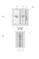
図1は、本実施形態に係る半導体装置を模式的に例示する断面図である。
図1に示すように、本実施形態に係る半導体装置1においては、単結晶シリコンからなる基板2が設けられており、基板2の表面の素子領域Aには、複数の素子3が形成されている。素子3は、例えば、半導体装置1の本来の機能を実現する素子であり、半導体回路を構成する素子である。素子3は、例えば、トランジスタ若しくはダイオードなどの能動素子、又は抵抗若しくは容量などの能動素子である。また、基板2上には、素子3を覆うように、層間絶縁膜4が形成されている。なお、本明細書においては、基板2における素子3が形成されている表面側を「上」とし、この表面に垂直な方向に沿って基板2から遠ざかる方向を「直上」とする。Hereinafter, embodiments of the present invention will be described with reference to the drawings.
FIG. 1 is a cross-sectional view schematically illustrating the semiconductor device according to this embodiment.
As shown in FIG. 1, in the
そして、層間絶縁膜4上における保護領域Bには、複数の多結晶シリコン層5が形成されている。保護領域Bは、素子領域Aの直上域の少なくとも一部を含む領域である。すなわち、基板2の表面に垂直な方向から見て(以下、「平面視で」という)、素子領域Aの少なくとも一部と、保護領域Bの少なくとも一部とは、重なり合っている。多結晶シリコン層5は、例えば、プラズマCVD法(Chemical Vapor Deposition法:化学気相成長法)によって堆積され、CMP(Chemical Mechanical Polishing:化学的機械研磨)によって上面が平坦化され、フォトリソグラフィ法によってパターニングされたものである。また、各多結晶シリコン層5内には、例えば1個の素子6が形成されている。素子6は、例えば、素子3を保護する保護素子であり、例えば、静電気などに起因するサージ電圧から素子3を保護する静電耐圧用保護素子であり、例えば、ダイオード、トランジスタ又はサイリスタである。更に、層間絶縁膜4上には、多結晶シリコン層5を覆うように、層間絶縁膜7が設けられている。 A plurality of
また、層間絶縁膜7上におけるパッド領域Cに、パッド8が設けられている。パッド領域Cは、素子領域Aの直上域であって保護領域Bの直上域である領域の少なくとも一部を含む領域である。すなわち、平面視で、素子領域A、保護領域B及びパッド領域Cは、少なくとも部分的に重なり合っている。パッド8は、例えば、金ワイヤーなどが超音波ボンディングされることにより、又はパッド8上に金バンプ若しくは銅バンプなどのバンプが形成されることにより、素子3などからなる半導体装置1の内部回路や素子6などからなる保護回路を、半導体装置1の外部に接続するものである。 A
次に、本実施形態の作用効果について説明する。
本実施形態においては、素子領域Aの直上域の少なくとも一部を含む領域(以下、「直上域近傍」という)に保護領域Bを設け、この保護領域B内に多結晶シリコン層5を形成し、この多結晶シリコン層5内に素子6を形成している。これにより、半導体装置1において、素子6を配置するための専用スペースを設ける必要がなく、半導体装置1の小型化を図ることができる。これにより、ダイサイズが小さく高密度な半導体パッケージ、例えば、BGA(Ball Grid Array)パッケージ、CSP(Chip Size Package)及びフリップチップパッケージなどを実現することができる。Next, the effect of this embodiment is demonstrated.
In the present embodiment, a protection region B is provided in a region including at least a part of the region immediately above the element region A (hereinafter referred to as “near the region immediately above”), and the
また、素子6は基板2に対して、層間絶縁膜4を介して離隔しているため、素子6と基板2との間には寄生容量が実質的に発生しない。この結果、寄生容量に起因する電力の消費を抑えることができる。これに対して、従来の半導体装置のように、イオン注入などの方法により、基板2の表面に素子6を作り込んだ場合は、基板2における素子6を形成している部分とそれ以外の部分とが、薄い空乏層を介して対向することになる。このため、大きな寄生容量が発生する。 Further, since the
更に、多結晶シリコン層5内に形成した素子6は、単結晶シリコン基板2の表面に形成した素子3と比較すれば、制御性が劣る可能性はあるが、素子6を静電耐圧用保護素子とすれば、それほど高い制御性は必要とされないため、実用上問題は生じない。なお、素子6の制御性を十分に高くすることができれば、素子6を通常の機能素子として形成することも可能である。例えば、NPN型トランジスタ及びPNP型トランジスタなどの能動素子、並びに抵抗などの受動素子として形成することも可能である。 Furthermore, although the
一方、素子3は単結晶シリコンからなる基板2の表面に形成しているため、高い特性を得ることができる。かつ、素子3の設計及び製造プロセスに関しては、従来の技術をそのまま活かすことができる。また、素子6は、多結晶シリコン層を堆積させ、上面を平坦化し、パターニングし、これにイオンを打ち込むという通常の方法で形成することができるため、作製が容易である。かつ、素子6の形成にあたり、素子3の設計及び製造プロセスに影響を及ぼすことがないので、素子3は、従来の技術をそのまま活かすことができる。 On the other hand, since the
更にまた、一般に、半導体装置においては、半導体装置の内部を外部に接続するためのパッドが設けられている。そして、パッケージ組立の制約上、パッドにはある程度の面積が必要とされる。このため、従来の半導体装置においては、パッドの面積が半導体装置全体の面積において大きな割合を占めることがあり、これが静電耐圧用保護素子の存在と共に半導体装置の小型化を阻害していた。すなわち、最終的なチップサイズが、その半導体装置の本質的な機能を実現する素子領域ではなく、静電耐圧要保護素子及びパッドなどの本質的でない要因によって支配されるような製品も存在していた。 Furthermore, generally, in a semiconductor device, a pad for connecting the inside of the semiconductor device to the outside is provided. Further, a certain amount of area is required for the pad due to restrictions on package assembly. For this reason, in the conventional semiconductor device, the area of the pad may occupy a large proportion of the total area of the semiconductor device, and this has hindered the miniaturization of the semiconductor device together with the presence of the electrostatic withstand voltage protection element. In other words, there are products in which the final chip size is not controlled by an element region that realizes the essential function of the semiconductor device, but is controlled by non-essential factors such as an electrostatic withstand voltage protection element and a pad. It was.
これに対して、本実施形態に係る半導体装置1においては、素子領域A及び保護領域Bの直上域近傍にパッド領域Cを設けることにより、パッド8を設けるための専用スペースを設ける必要がない。これにより、パッド領域Cによって半導体装置1の小型化が阻害されることがなくなり、半導体装置1を更に小型化することができる。また、半導体装置全体のサイズが増大することを憂慮することなく、十分な面積を持つパッドを十分な数だけ形成することができため、パッケージの組立の制約を大幅に緩和することができる。 On the other hand, in the
また、パッド8と素子3との間には多結晶シリコン層5及び層間絶縁膜7が介在するため、パッド8に金ワイヤーなどを超音波ボンディングしたり、パッド8上に金バンプ又は銅バンプなどのバンプを形成する際に、多結晶シリコン層5及び層間絶縁膜7が緩衝材として機能する。これにより、金ワイヤー又はバンプなどをパッド8にボンディングする際の発生する機械的なストレスが素子3に伝達することを抑制できる。この結果、半導体装置1のボンディングダメージを軽減することができる。 Further, since the
以下、本実施形態の効果を比較例と比較して定量的に説明する。
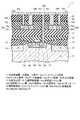
図2は、比較例に係る半導体装置を模式的に示す断面図であり、
図3(a)及び(b)並びに図4(a)及び(b)は、本実施形態の効果を模式的に示す平面図であり、各図の(a)は比較例に係る半導体装置を示し、(b)は本実施形態に係る半導体装置を示す。Hereinafter, the effect of this embodiment will be described quantitatively in comparison with a comparative example.
FIG. 2 is a cross-sectional view schematically showing a semiconductor device according to a comparative example.
3 (a) and 3 (b) and FIGS. 4 (a) and 4 (b) are plan views schematically showing the effects of the present embodiment. FIG. 3 (a) shows a semiconductor device according to a comparative example. (B) shows the semiconductor device according to the present embodiment.
図2に示すように、比較例に係る半導体装置101においては、単結晶シリコン基板2の表面に、素子領域A及び保護領域Bが別々に設定され、素子領域Aに機能素子3が形成され、保護領域Bに保護素子6が形成されている。すなわち、機能素子3及び保護素子6は同一面上に形成されている。また、基板2上には、機能素子3及び保護素子6を覆うように層間絶縁膜7が設けられており、層間絶縁膜7上におけるパッド領域Cには、パッド8が設けられている。パッド領域Cは、素子領域Aの直上域及び保護領域Bの直上域から外れている。すなわち、平面視で、素子領域A、保護領域B及びパッド領域Cは、重なり合っていない。 As shown in FIG. 2, in the
以下、数値の一例を挙げて説明する。
図3(a)に示すように、比較例に係る半導体装置101において保護素子がダイオードである場合には、例えば、機能素子3が形成されている素子領域Aは、平面視で、半導体装置101全体の70%の面積を占め、保護素子6(ダイオード)が形成されている保護領域Bは10%の面積を占め、パッド8が形成されているパッド領域Cは20%の面積を占める。Hereinafter, an example of a numerical value will be described.
As illustrated in FIG. 3A, when the protection element is a diode in the
この場合において、本実施形態によれば、図3(b)に示すように、上述の如く、半導体装置の構造を立体構造とすることにより、全体の10%の面積を占める保護領域Bを70%の面積を占める素子領域Aの直上域内に配置することができる。また、全体の20%の面積を占めるパッド領域Cも、素子領域Aの直上域内であって保護領域Bの直上域を含む領域に配置することができる。このため、平面視で、半導体装置1に必要とされる面積は、素子領域Aの面積のみとなる。従って、本実施形態に係る半導体装置1の面積は、比較例に係る半導体装置101の面積の70%で足り、半導体装置の小型化を図ることができる。 In this case, according to the present embodiment, as shown in FIG. 3B, as described above, the protection region B occupying an area of 10% of the whole is obtained by making the structure of the semiconductor device into a three-dimensional structure. It can be arranged in the region immediately above the element region A occupying an area of%. Further, the pad region C occupying 20% of the entire area can also be arranged in a region directly above the element region A and including a region directly above the protection region B. For this reason, the area required for the
また、図4(a)に示すように、比較例に係る半導体装置101の保護素子6がサイリスタである場合においては、例えば、機能素子3が形成されている素子領域Aは、平面視で、半導体装置101全体の40%の面積を占め、保護素子6(サイリスタ)が形成されている保護領域Bは50%の面積を占め、パッド8が形成されているパッド領域Cは10%の面積を占める。 4A, when the
この場合において、本実施形態によれば、図4(b)に示すように、全体の50%の面積を占める保護領域Bを40%の面積を占める素子領域Aの直上域を含む領域に配置し、全体の10%を占めるパッド領域Cを素子領域A及び保護領域Bの直上域内に配置することができる。この結果、平面視で、半導体装置1に必要とされる面積は、保護領域Bの面積のみとなる。従って、本実施形態に係る半導体装置1の面積は、比較例に係る半導体装置101の面積の50%で足りる。このように、本例においては、半導体装置を、より一層小型化することができる。 In this case, according to the present embodiment, as shown in FIG. 4B, the protection region B occupying 50% of the entire area is arranged in a region including the region immediately above the element region A occupying 40% of the area. In addition, the pad region C occupying 10% of the entire region can be arranged in the region immediately above the element region A and the protection region B. As a result, the area required for the
なお、本実施形態においては、素子3及び6を基板2の表面及び多結晶シリコン層5の2層に分けて設ける例を示したが、本発明はこれに限定されず、素子を3層以上の層に分けて設けてもよい。 In the present embodiment, the example in which the
以下、本実施形態を具現化するための具体例について説明する。
先ず、第1の具体例について説明する。
図5は、本具体例に係る半導体装置を例示する断面図であり、
図6は、この半導体装置を例示する回路図である。Hereinafter, a specific example for realizing the present embodiment will be described.
First, a first specific example will be described.
FIG. 5 is a cross-sectional view illustrating a semiconductor device according to this example.
FIG. 6 is a circuit diagram illustrating this semiconductor device.
図5に示すように、本具体例に係る半導体装置11においては、例えばP型の単結晶シリコンからなる基板12が設けられている。基板12の表面における素子領域には、内部回路25(図6参照)が形成されており、内部回路25には複数の素子13が設けられている。素子13は、半導体装置11の本来の機能を実現する機能素子であり、例えば、基板12の表面に形成されたNMOSFET(N type Metal Oxide Semiconductor Field Effect Transistor:N型金属酸化物半導体電界効果トランジスタ)である。なお、図5においては、内部回路25の構成要素として1個の素子13のみを図示しているが、実際には、内部回路25は、多数且つ多種類の能動素子及び受動素子により構成されている。 As shown in FIG. 5, in the
素子13においては、基板12の表層部に、1対のN+領域が形成されており、ソース・ドレイン領域13aとなっている。また、N+領域13a間の領域はチャネル領域13bとなっている。更に、ソース・ドレイン領域13a及びチャネル領域13b上には、ゲート絶縁膜13cが形成されており、その上には、例えば多結晶シリコンからなるゲート電極13dが設けられている。また、基板12の表面における素子13間の領域には、素子分離膜14が形成されており、基板12の内部における素子分離膜14の直下域には、P型の反転防止層15が形成されている。ソース・ドレイン領域13a及び反転防止層15は、局所的なイオン注入によって形成されている。In the
更に、基板12上には、層間絶縁膜16が設けられており、素子13及び素子分離膜14を覆っている。層間絶縁膜16上には金属配線(図示せず)が設けられている。更にまた、層間絶縁膜16上には、層間絶縁膜17が設けられており、金属配線を覆っている。 Further, an
そして、層間絶縁膜17上における素子領域の直上域の少なくとも一部を含む領域(直上域近傍)には、保護領域が設定されている。そして、層間絶縁膜17上における保護領域には、多結晶シリコン(ポリシリコン)からなる多結晶シリコン層18a及び18b(以下、総称して「多結晶シリコン層18」ともいう)が設けられている。多結晶シリコン層18は、例えば、シリコンが減圧(LP:Low pressure)CVDによって多結晶成長するように堆積された後、CMPによって上面を平坦化され、フォトリソグラフィ法によって選択的にエッチングされてパターニングされたものである。 A protective region is set in a region including at least a part of the region immediately above the element region on the interlayer insulating film 17 (near the region immediately above). In the protective region on the
多結晶シリコン層18aにおける一部には、P型不純物が注入されており、P型部分18pとなっている。また、各多結晶シリコン層18における残部には、N型不純物が注入されており、N型部分18nとなっている。P型部分18p及びN型部分18nは、共に多結晶シリコン層18の厚さ方向全体にわたって形成されており、多結晶シリコン層18の上面及び下面の双方において露出している。また、P型部分18pとN型部分18nとは相互に接しており、PN接合界面を形成している。これにより、多結晶シリコン層18aにおいては、P型部分18p及びN型部分18nからなるダイオード19aが形成されている。同様に、多結晶シリコン層18bにおいては、ダイオード19bが形成されている。ダイオード19a及び19b(以下、総称して「ダイオード19」ともいう)は、素子13を静電気放電から保護する保護素子である。 A part of the
層間絶縁膜17上の全面には、多結晶シリコン層18a及び18bを覆うように、層間絶縁膜20が形成されている。そして、層間絶縁膜20上における素子領域及び保護領域の双方の直上域の少なくとも一部を含む領域(直上域近傍)には、パッド領域が設定されている。層間絶縁膜20上におけるパッド領域には、パッド21(図6参照)が形成されている。 An interlayer insulating
また、層間絶縁膜20上の全面には、トップパッシベーション膜22が形成されている。トップパッシベーション膜22におけるパッド21の直上域は開口されており、パッド21が露出している。パッド21は、金ワイヤーなどがボンディングされることにより、又は、その上に金バンプ若しくは銅バンプなどのバンプが形成されることにより、外部と接続される。更に、トップパッシベーション膜22上には、金属配線23a、23b、23cが形成されている。更にまた、層間絶縁膜20及びトップパッシベーション膜22を貫通するように、ビア24a乃至24dが設けられている。更にまた、ゲート絶縁膜13c、層間絶縁膜16乃至20及びトップパッシベーション膜22を貫通するように、ビア24eが設けられている。 A
多結晶シリコン層18a(ダイオード19a)のP型部分18pは、ビア24aを介して、金属配線23aに接続されている。金属配線23aには接地電位(GND)が印加されている。また、多結晶シリコン層18aのN型部分18nは、ビア24bを介して、金属配線23bに接続されている。更に、多結晶シリコン層18b(ダイオード19b)のP型部分18pは、ビア24cを介して、金属配線23bに接続されている。更にまた、多結晶シリコン層18bのN型部分18nは、ビア24dを介して、金属配線23cに接続されている。金属配線23cには電源電位(Vcc)が印加されている。そして、金属配線23bは、ビア24eを介して、素子13のソース・ドレイン領域13aのうちの一方に接続されている。これにより、金属配線23は内部回路25(図6参照)に接続されている。また、金属配線23は、パッド21(図6参照)にも接続されている。なお、全ての多結晶シリコン層18において、取出し部、すなわち、多結晶シリコン層18とビア24との接合部には、この取出し部が内包されている部分と同じ導電型であって、オーミック接続がとれる程度に濃度が高い高濃度層(図示せず)が形成されている。 The P-
これにより、図6に示すように、半導体装置11においては、パッド21を内部回路25に接続する配線(金属配線23b)に、アノードが接地電位配線(金属配線23a)に接続されたダイオード19aのカソードと、カソードが電源電位配線(金属配線23c)に接続されたダイオード19bのアノードとが接続されている。この結果、ダイオード19a及び19bが、内部回路25の静電耐圧用保護素子として機能する。 Thus, as shown in FIG. 6, in the
次に、本具体例の作用効果について説明する。
図5及び図6に示すように、半導体装置11においては、基板12の表面の素子領域に、素子13を含む内部回路25が形成されており、層間絶縁膜17上における素子領域の直上域近傍に、保護領域が設定されている。そして、この保護領域には多結晶シリコン層18が形成されており、多結晶シリコン層18内には保護素子としてのダイオード19が作り込まれている。これにより、半導体装置11においては、保護素子を配置するための専用のスペースを設ける必要がなく、小型化を図ることができる。Next, the effect of this example is demonstrated.
As shown in FIGS. 5 and 6, in the
また、層間絶縁膜22上における素子領域及び保護領域の直上域近傍にはパッド領域が設定されており、このパッド領域にはパッド21が形成されている。これにより、半導体装置11においては、パッドを配置するための専用のスペースを設ける必要がなく、より一層の小型化を図ることができる。 A pad region is set in the vicinity of the element region on the
更に、一般に、パッド21に金ワイヤーなどをボンディングしたり、パッド21上に金バンプ又は銅バンプなどのバンプを形成する際には、パッド21に機械的なストレスが不可避的に印加され、このストレスが内部回路25に伝達されると、内部回路25に損傷(ボンディングダメージ)を与える可能性がある。しかしながら、本具体例においては、パッド21と内部回路25との間に多結晶シリコン層18及び層間絶縁膜20が配置されているため、パッド21に加えられたストレスが内部回路25に伝達されることを抑制できる。これにより、内部回路25が損傷を受けることを防止することができる。 Furthermore, generally, when bonding a gold wire or the like to the pad 21 or forming a bump such as a gold bump or a copper bump on the pad 21, mechanical stress is inevitably applied to the pad 21. Is transmitted to the
次に、本発明の第2の具体例について説明する。
本具体例に係る半導体装置は、前述の第1の具体例に係る半導体装置11(図5参照)と比較して、ダイオード19の構成が異なっている。すなわち、ダイオード19においては、多結晶シリコン層18の略全体がP型部分18pとなっており、P型部分18pの内部にN型部分18nが形成されている。N型部分18nは多結晶シリコン層18の上面に露出しており、下面には露出していない。また、前述の第1の具体例と同様に、全ての多結晶シリコン層18において、取出し部には、この取出し部が内包されている部分と同じ導電型であって、オーミック接続がとれる程度に濃度が高い高濃度層(図示せず)が形成されている。本具体例によれば、前述の第1の具体例と比較して、ダイオードにおけるPN接合界面の面積を増大させることができる。本具体例における上記以外の構成及び作用効果は、前述の第1の具体例と同様である。Next, a second specific example of the present invention will be described.
The semiconductor device according to this example is different from the
次に、本発明の第3の具体例について説明する。
本具体例に係る半導体装置においては、前述の第2の具体例とは逆に、多結晶シリコン層18の略全体がN型部分18nとなっており、N型部分18nの内部にP型部分18pが形成されている。P型部分18pは多結晶シリコン層18の上面に露出しており、下面には露出していない。また、多結晶シリコン層18の取出し部には、高濃度層が形成されている。そして、このような多結晶シリコン層18により、保護素子としてのダイオードが構成されている。本具体例における上記以外の構成及び作用効果は、前述の第2の具体例と同様である。Next, a third specific example of the present invention will be described.
In the semiconductor device according to this specific example, contrary to the second specific example described above, substantially the entire polycrystalline silicon layer 18 is an N-
次に、本発明の第4の具体例について説明する。
図7は、本具体例に係る半導体装置を例示する回路図であり、
図8は、この半導体装置を模式的に例示する斜視図であり、
図9(a)は、図8に示すPNP型トランジスタを例示する斜視図であり、(b)は、図8に示すNPN型トランジスタを例示する斜視図である。Next, a fourth specific example of the present invention will be described.
FIG. 7 is a circuit diagram illustrating a semiconductor device according to this example.
FIG. 8 is a perspective view schematically illustrating this semiconductor device.
FIG. 9A is a perspective view illustrating the PNP transistor illustrated in FIG. 8, and FIG. 9B is a perspective view illustrating the NPN transistor illustrated in FIG.
図7に示すように、本具体例に係る半導体装置51においては、内部回路52が設けられており、この内部回路52には、I/O(Input/Output)パッド53a及びGNDパッド53bが接続されている。I/Oパッド53aは、内部回路52に対して外部から信号を入出力するためのパッドであり、GNDパッド53bは、内部回路52に対して接地電位を供給するためのパッドである。 As shown in FIG. 7, an
そして、内部回路52をI/Oパッド53aに接続する配線54aと、内部回路52をGNDパッド53bに接続する配線54bとの間に、保護回路55a及び55bが並列に接続されている。保護回路55aは、+サージに対するサイリスタ型の保護回路であり、保護回路55bは、−サージに対するサイリスタ型の保護回路である。
保護回路55a(+サージ回路)においては、配線54aと配線54bとの間に、負荷56、PNP型トランジスタ57及び抵抗58がこの順に直列に接続されている。また、保護回路55aにはNPN型トランジスタ59及び負荷60が設けられている。NPN型トランジスタ59のコレクタはPNP型トランジスタ57のベースに接続され、エミッタは配線54bに接続され、ベースはPNP型トランジスタ57のコレクタと抵抗58との間のノードN1に接続されている。また、負荷60は、PNP型トランジスタ57のベースとNPN型トランジスタ59のコレクタとの間のノードN2と、配線54bとの間に接続されている。 In the
保護回路55b(−サージ回路)においては、配線54aと配線54bとの間に、抵抗61及びPNP型トランジスタ62がこの順に直列に接続されている。また、保護回路55bにはNPN型トランジスタ63及び負荷64が設けられている。NPN型トランジスタ63のコレクタはPNP型トランジスタ62のベースに接続されており、エミッタは配線54aに接続されており、ベースは抵抗61とPNP型トランジスタ62との間のノードN3に接続されている。また、負荷64は、PNP型トランジスタ62のベースとNPN型トランジスタ63のコレクタとの間のノードN4と、配線54aとの間に接続されている。なお、上述の負荷56、60及び64は、例えばダイオードである。 In the
図8に示すように、半導体装置51においては、例えばP型の単結晶シリコンからなる基板71が設けられており、この基板71上に多層配線層72が設けられている。そして、内部回路52は基板71の表面に形成されており、保護回路55a及び55bは多層配線層72内における内部回路52の直上域に形成されており、I/Oパッド53a及びGNDパッド53bなどのパッド53は、多層配線層72上における内部回路52の直上域であって保護回路55a又は55bの直上域に形成されている。なお、図8においては、保護回路55a(+サージ回路)及び層間絶縁膜は図示を省略されている。 As shown in FIG. 8, in the
また、多層配線層72内には、パターニングされた多結晶シリコン層が複数設けられており、この多結晶シリコン層により、抵抗58及び61、PNP型トランジスタ57及び62、NPN型トランジスタ59及び63、並びに、ダイオードからなる負荷56、60及び64が形成されている。更に、多層配線層72内には、配線54a及び54b並びに保護回路55a内及び保護回路55b内の各素子の相互間を接続する配線及びビアも形成されている。 In addition, a plurality of patterned polycrystalline silicon layers are provided in the
例えば、図9(a)に示すように、PNP型トランジスタ62においては、直方体形状にパターニングされた多結晶シリコン層の両端部にP型不純物が注入されてP型部分62a及び62cとなっており、中央部にN型不純物が注入されてN型部分62bとなっている。すなわち、P型部分62aとP型部分62cとにより、N型部分62bが挟まれている。一方、図9(b)に示すように、NPN型トランジスタ63においては、直方体形状にパターニングされた多結晶シリコン層の両端部にN型不純物が注入されてN型部分63a及び63cとなっており、中央部にP型不純物が注入されてP型部分63bとなっている。すなわち、N型部分63aとN型部分63cとにより、P型部分63bが挟まれている。 For example, as shown in FIG. 9A, in the
そして、PNP型トランジスタ62のP型部分62aはビアを介して配線54bに接続されており、N型部分62bはビア及び配線を介して負荷64及びNPN型トランジスタ63のN型部分63aに接続されており、P型部分62cはビア及び配線を介して抵抗61及びNPN型トランジスタ63のP型部分63bに接続されており、NPN型トランジスタ63のN型部分63cは配線54aに接続されている。また、各トランジスタの取出し部には、高濃度層が形成されている。すなわち、PNP型トランジスタ62のP型部分62a及び62cの上面におけるビアと接続する部分には、それぞれ、オーミック接続が可能となる程度にP型不純物が導入された高濃度P型層(図示せず)が形成されており、N型部分62bの上面におけるビアと接続する部分には、オーミック接続が可能となる程度にN型不純物が導入された高濃度N型層(図示せず)が形成されている。同様に、NPN型トランジスタ63のN型部分63a及び63cにおけるビアとの接続部分には高濃度N型層(図示せず)が形成されており、P型部分63bにおけるビアとの接続部分には高濃度P型層(図示せず)が形成されている。 The P-
本具体例においても、内部回路52の直上域に保護回路55a及び55bが設けられており、その直上域にパッド53が設けられているため、前述の第1の具体例と同様な効果を得ることができる。 Also in this specific example, the
次に、本発明の第5の具体例について説明する。
本具体例に係る半導体装置においては、前述の第4の具体例と比較して、保護回路を構成するトランジスタの構成が異なっている。すなわち、本具体例に係る半導体装置においては、PNP型トランジスタ62において、P型部分62a内にN型部分62bが形成されており、N型部分62b内にP型部分62cが形成されている。そして、N型部分62b及びP型部分62cは、PNP型トランジスタ62を構成する多結晶シリコン層の上面に露出し、下面には露出していない。Next, a fifth specific example of the present invention will be described.
In the semiconductor device according to this example, the configuration of the transistors constituting the protection circuit is different from that of the above-described fourth example. That is, in the semiconductor device according to this example, in the
同様に、NPN型トランジスタ63においては、N型部分63a内にP型部分63bが形成されており、P型部分63b内にN型部分63cが形成されている。そして、P型部分63b及びN型部分63cは、NPN型トランジスタ63を構成する多結晶シリコン層の上面に露出し、下面には露出していない。そして、前述の第4の具体例と同様に、PNP型トランジスタ62及びNPN型トランジスタ63の取出し部には、それぞれ高濃度層が形成されている。本具体例における上記以外の構成及び作用効果は、前述の第4の具体例と同様である。 Similarly, in the
以上、実施形態及び具体例を参照して本発明を説明したが、本発明はこれらの実施形態及び具体例に限定されるものではない。例えば、前述のいずれかの実施形態又は具体例に対して、当業者が適宜、構成要素の追加、削除、設計変更を行ったものも、本発明の要旨を備えている限り、本発明の範囲に含有される。 Although the present invention has been described above with reference to the embodiments and specific examples, the present invention is not limited to these embodiments and specific examples. For example, any of the above-described embodiments or specific examples, in which a person skilled in the art appropriately added, deleted, or changed a design, includes the scope of the present invention as long as the gist of the present invention is included. Contained in
1、11、51、101 半導体装置、2、12、71 基板、3、6、13 素子、4、7、16、17、20 層間絶縁膜、5、18、18a、18b 多結晶シリコン層、8 パッド、13a ソース・ドレイン領域、13b チャネル領域、13c ゲート絶縁膜、13d ゲート電極、14 素子分離膜、15 反転防止層、18p、62a、62c、63b P型部分、18n、62b、63a、63c N型部分、19a、19b ダイオード、21 パッド、22 トップパッシベーション膜、23a、23b、23c 金属配線、24a、24b、24c、24d、24e ビア、25、52 内部回路、53 パッド、53a I/Oパッド、53b GNDパッド、54a、54b 配線、55a、55b 保護回路、56、60、64 負荷、57、62 PNP型トランジスタ、58、61 抵抗、59、63 NPN型トランジスタ、72 多層配線層、A 素子領域、B 保護領域、C パッド領域、N1、N2、N3、N4 ノード1, 11, 51, 101
Claims (5)
Translated fromJapanese前記基板の表面の第1領域に形成された第1の素子と、
前記基板上に形成された第1の層間絶縁膜と、
前記第1の層間絶縁膜上における第2領域に形成された多結晶シリコン層と、
前記多結晶シリコン層内に形成された第2の素子と、
前記第1の層間絶縁膜上に前記多結晶シリコン層を覆うように形成された第2の層間絶縁膜と、
前記第2の層間絶縁膜上における第3領域に形成されたパッドと、
を備え、
前記第2領域は、前記第1領域の直上域の少なくとも一部を含む領域であり、前記第3領域は、前記第1領域の直上域であって前記第2領域の直上域である領域の少なくとも一部を含む領域であることを特徴とする半導体装置。A substrate made of single crystal silicon;
A first element formed in a first region of the surface of the substrate;
A first interlayer insulating film formed on the substrate;
A polycrystalline silicon layer formed in a second region on the first interlayer insulating film;
A second element formed in the polycrystalline silicon layer;
A second interlayer insulating film formed on the first interlayer insulating film so as to cover the polycrystalline silicon layer;
A pad formed in a third region on the second interlayer insulating film;
With
The second region is a region including at least a part of the region directly above the first region, and the third region is a region immediately above the first region and directly above the second region. A semiconductor device including a region including at least a part thereof.
Priority Applications (2)
| Application Number | Priority Date | Filing Date | Title |
|---|---|---|---|
| JP2007055967AJP2008218818A (en) | 2007-03-06 | 2007-03-06 | Semiconductor device |
| US12/025,299US8004067B2 (en) | 2007-03-06 | 2008-02-04 | Semiconductor apparatus |
Applications Claiming Priority (1)
| Application Number | Priority Date | Filing Date | Title |
|---|---|---|---|
| JP2007055967AJP2008218818A (en) | 2007-03-06 | 2007-03-06 | Semiconductor device |
Publications (1)
| Publication Number | Publication Date |
|---|---|
| JP2008218818Atrue JP2008218818A (en) | 2008-09-18 |
Family
ID=39838485
Family Applications (1)
| Application Number | Title | Priority Date | Filing Date |
|---|---|---|---|
| JP2007055967APendingJP2008218818A (en) | 2007-03-06 | 2007-03-06 | Semiconductor device |
Country Status (2)
| Country | Link |
|---|---|
| US (1) | US8004067B2 (en) |
| JP (1) | JP2008218818A (en) |
Cited By (5)
| Publication number | Priority date | Publication date | Assignee | Title |
|---|---|---|---|---|
| WO2012121255A1 (en)* | 2011-03-09 | 2012-09-13 | ルネサスエレクトロニクス株式会社 | Semiconductor device |
| JP2013093500A (en)* | 2011-10-27 | 2013-05-16 | Fuji Electric Co Ltd | Semiconductor device and testing method of the same |
| JP2014207413A (en)* | 2013-04-16 | 2014-10-30 | 富士電機株式会社 | Semiconductor device |
| WO2015025753A1 (en)* | 2013-08-19 | 2015-02-26 | 株式会社村田製作所 | Esd protection function-equipped thin-film capacitor device and method for producing same |
| JP2018133359A (en)* | 2017-02-13 | 2018-08-23 | 株式会社豊田中央研究所 | Semiconductor device |
Citations (4)
| Publication number | Priority date | Publication date | Assignee | Title |
|---|---|---|---|---|
| JPS63217632A (en)* | 1987-03-05 | 1988-09-09 | Nec Corp | Semiconductor device |
| JPH05226404A (en)* | 1991-09-06 | 1993-09-03 | Rohm Co Ltd | Semiconductor device |
| JPH06204284A (en)* | 1993-01-08 | 1994-07-22 | Nec Yamagata Ltd | Semiconductor device |
| JPH1168040A (en)* | 1997-08-19 | 1999-03-09 | Sony Corp | Input protective circuit and semiconductor circuit using the same |
Family Cites Families (6)
| Publication number | Priority date | Publication date | Assignee | Title |
|---|---|---|---|---|
| JPH0473970A (en) | 1990-07-16 | 1992-03-09 | Fuji Electric Co Ltd | MOS type semiconductor device |
| US5139959A (en) | 1992-01-21 | 1992-08-18 | Motorola, Inc. | Method for forming bipolar transistor input protection |
| JP3217560B2 (en) | 1993-11-15 | 2001-10-09 | 株式会社東芝 | Semiconductor device |
| US5589415A (en) | 1995-06-07 | 1996-12-31 | Sgs-Thomson Microelectronics, Inc. | Method for forming a semiconductor structure with self-aligned contacts |
| JP3642466B2 (en) | 1999-04-13 | 2005-04-27 | 関西日本電気株式会社 | Manufacturing method of semiconductor device |
| TW584953B (en) | 2003-04-25 | 2004-04-21 | Toppoly Optoelectronics Corp | ESD protection device with thick poly film, electronic device and method for forming the same |
- 2007
- 2007-03-06JPJP2007055967Apatent/JP2008218818A/enactivePending
- 2008
- 2008-02-04USUS12/025,299patent/US8004067B2/ennot_activeExpired - Fee Related
Patent Citations (4)
| Publication number | Priority date | Publication date | Assignee | Title |
|---|---|---|---|---|
| JPS63217632A (en)* | 1987-03-05 | 1988-09-09 | Nec Corp | Semiconductor device |
| JPH05226404A (en)* | 1991-09-06 | 1993-09-03 | Rohm Co Ltd | Semiconductor device |
| JPH06204284A (en)* | 1993-01-08 | 1994-07-22 | Nec Yamagata Ltd | Semiconductor device |
| JPH1168040A (en)* | 1997-08-19 | 1999-03-09 | Sony Corp | Input protective circuit and semiconductor circuit using the same |
Cited By (9)
| Publication number | Priority date | Publication date | Assignee | Title |
|---|---|---|---|---|
| WO2012121255A1 (en)* | 2011-03-09 | 2012-09-13 | ルネサスエレクトロニクス株式会社 | Semiconductor device |
| JP5583266B2 (en)* | 2011-03-09 | 2014-09-03 | ルネサスエレクトロニクス株式会社 | Semiconductor device |
| US9263399B2 (en) | 2011-03-09 | 2016-02-16 | Renesas Electronics Corporation | Semiconductor device with electro-static discharge protection device above semiconductor device area |
| US9530769B2 (en) | 2011-03-09 | 2016-12-27 | Renesas Electronics Corporation | Semiconductor device with electro-static discharge protection device above semiconductor device area |
| JP2013093500A (en)* | 2011-10-27 | 2013-05-16 | Fuji Electric Co Ltd | Semiconductor device and testing method of the same |
| JP2014207413A (en)* | 2013-04-16 | 2014-10-30 | 富士電機株式会社 | Semiconductor device |
| WO2015025753A1 (en)* | 2013-08-19 | 2015-02-26 | 株式会社村田製作所 | Esd protection function-equipped thin-film capacitor device and method for producing same |
| JP5704291B1 (en)* | 2013-08-19 | 2015-04-22 | 株式会社村田製作所 | Thin film capacitor device with ESD protection function and manufacturing method thereof |
| JP2018133359A (en)* | 2017-02-13 | 2018-08-23 | 株式会社豊田中央研究所 | Semiconductor device |
Also Published As
| Publication number | Publication date |
|---|---|
| US20080315197A1 (en) | 2008-12-25 |
| US8004067B2 (en) | 2011-08-23 |
Similar Documents
| Publication | Publication Date | Title |
|---|---|---|
| US10262947B2 (en) | Active chip on carrier or laminated chip having microelectronic element embedded therein | |
| US5514892A (en) | Electrostatic discharge protection device | |
| TWI425605B (en) | A semiconductor device and a back-illuminated solid-state imaging device | |
| US8653641B2 (en) | Integrated circuit device | |
| US7038280B2 (en) | Integrated circuit bond pad structures and methods of making | |
| US7629652B2 (en) | Semiconductor device with signal wirings that pass through under the output electrode pads and dummy wirings near the peripheral portion | |
| US6489689B2 (en) | Semiconductor device | |
| TWI496245B (en) | Semiconductor device | |
| TWI416706B (en) | Electrostatic discharge protection structure of three-dimensional integrated circuit | |
| US7629689B2 (en) | Semiconductor integrated circuit having connection pads over active elements | |
| US8067789B2 (en) | Semiconductor integrated circuit device | |
| TWI593031B (en) | Semiconductor integrated circuit device | |
| JP2012502477A (en) | System and method enabling ESD protection of 3-D stacked devices | |
| JP2014086498A (en) | Semiconductor element manufacturing method | |
| JP2010129958A (en) | Semiconductor device, and manufacturing method thereof | |
| JP7612724B2 (en) | Solid-state imaging device and method for manufacturing the same | |
| JP2008218818A (en) | Semiconductor device | |
| JP2010135391A (en) | Semiconductor device and method for manufacturing the same | |
| JP2017212432A (en) | Semiconductor device | |
| JP2005294634A (en) | Semiconductor device and manufacturing method thereof | |
| JPH08236706A (en) | Semiconductor integrated circuit element and semiconductor device incorporating the element | |
| JP2006202866A (en) | Semiconductor apparatus | |
| JP2009038099A (en) | Semiconductor device | |
| US20240021648A1 (en) | Semiconductor device | |
| JP5955645B2 (en) | Semiconductor device |
Legal Events
| Date | Code | Title | Description |
|---|---|---|---|
| A621 | Written request for application examination | Free format text:JAPANESE INTERMEDIATE CODE: A621 Effective date:20090309 | |
| A977 | Report on retrieval | Free format text:JAPANESE INTERMEDIATE CODE: A971007 Effective date:20120309 | |
| A131 | Notification of reasons for refusal | Free format text:JAPANESE INTERMEDIATE CODE: A131 Effective date:20120313 | |
| A02 | Decision of refusal | Free format text:JAPANESE INTERMEDIATE CODE: A02 Effective date:20120702 |