JP2008218684A - Method of fabricating semiconductor device - Google Patents
Method of fabricating semiconductor deviceDownload PDFInfo
- Publication number
- JP2008218684A JP2008218684AJP2007053704AJP2007053704AJP2008218684AJP 2008218684 AJP2008218684 AJP 2008218684AJP 2007053704 AJP2007053704 AJP 2007053704AJP 2007053704 AJP2007053704 AJP 2007053704AJP 2008218684 AJP2008218684 AJP 2008218684A
- Authority
- JP
- Japan
- Prior art keywords
- hydrogen
- nitride film
- silicon
- atoms
- film
- Prior art date
- Legal status (The legal status is an assumption and is not a legal conclusion. Google has not performed a legal analysis and makes no representation as to the accuracy of the status listed.)
- Pending
Links
- 238000004519manufacturing processMethods0.000titleclaimsabstractdescription25
- 239000004065semiconductorSubstances0.000titleclaimsabstractdescription14
- 229910052739hydrogenInorganic materials0.000claimsabstractdescription60
- 239000001257hydrogenSubstances0.000claimsabstractdescription58
- XUIMIQQOPSSXEZ-UHFFFAOYSA-NSiliconChemical group[Si]XUIMIQQOPSSXEZ-UHFFFAOYSA-N0.000claimsabstractdescription57
- 229910052581Si3N4Inorganic materials0.000claimsabstractdescription40
- HQVNEWCFYHHQES-UHFFFAOYSA-Nsilicon nitrideChemical compoundN12[Si]34N5[Si]62N3[Si]51N64HQVNEWCFYHHQES-UHFFFAOYSA-N0.000claimsabstractdescription40
- 238000000034methodMethods0.000claimsabstractdescription36
- 150000002431hydrogenChemical class0.000claimsabstractdescription32
- UFHFLCQGNIYNRP-UHFFFAOYSA-NHydrogenChemical compound[H][H]UFHFLCQGNIYNRP-UHFFFAOYSA-N0.000claimsabstractdescription31
- 238000000151depositionMethods0.000claimsabstractdescription25
- 230000008021depositionEffects0.000claimsabstractdescription25
- 125000004433nitrogen atomChemical groupN*0.000claimsabstractdescription21
- 229910052710siliconInorganic materials0.000claimsabstractdescription21
- 238000000231atomic layer depositionMethods0.000claimsabstractdescription16
- 229910052757nitrogenInorganic materials0.000claimsabstractdescription10
- 230000015572biosynthetic processEffects0.000claimsdescription73
- 125000004435hydrogen atomChemical group[H]*0.000claimsdescription25
- 150000004767nitridesChemical class0.000abstractdescription33
- 239000007789gasSubstances0.000description15
- 239000010703siliconSubstances0.000description14
- 239000000460chlorineSubstances0.000description12
- 125000001309chloro groupChemical groupCl*0.000description10
- IJGRMHOSHXDMSA-UHFFFAOYSA-NAtomic nitrogenChemical compoundN#NIJGRMHOSHXDMSA-UHFFFAOYSA-N0.000description8
- 239000010410layerSubstances0.000description8
- 125000006850spacer groupChemical group0.000description7
- QGZKDVFQNNGYKY-UHFFFAOYSA-NAmmoniaChemical compoundNQGZKDVFQNNGYKY-UHFFFAOYSA-N0.000description6
- 230000006866deteriorationEffects0.000description6
- MROCJMGDEKINLD-UHFFFAOYSA-NdichlorosilaneChemical compoundCl[SiH2]ClMROCJMGDEKINLD-UHFFFAOYSA-N0.000description6
- 229910007991Si-NInorganic materials0.000description4
- BLRPTPMANUNPDV-UHFFFAOYSA-NSilaneChemical compound[SiH4]BLRPTPMANUNPDV-UHFFFAOYSA-N0.000description4
- 229910006294Si—NInorganic materials0.000description4
- 125000004429atomChemical group0.000description4
- 229910052801chlorineInorganic materials0.000description4
- 239000002184metalSubstances0.000description4
- 229910000077silaneInorganic materials0.000description4
- 239000000758substrateSubstances0.000description4
- 239000002344surface layerSubstances0.000description4
- XLYOFNOQVPJJNP-UHFFFAOYSA-NwaterSubstancesOXLYOFNOQVPJJNP-UHFFFAOYSA-N0.000description4
- 229910021529ammoniaInorganic materials0.000description3
- 238000010586diagramMethods0.000description3
- 150000004703alkoxidesChemical class0.000description2
- SLLGVCUQYRMELA-UHFFFAOYSA-NchlorosiliconChemical compoundCl[Si]SLLGVCUQYRMELA-UHFFFAOYSA-N0.000description2
- GPTXWRGISTZRIO-UHFFFAOYSA-NchlorquinaldolChemical compoundClC1=CC(Cl)=C(O)C2=NC(C)=CC=C21GPTXWRGISTZRIO-UHFFFAOYSA-N0.000description2
- 238000009792diffusion processMethods0.000description2
- PZPGRFITIJYNEJ-UHFFFAOYSA-NdisilaneChemical compound[SiH3][SiH3]PZPGRFITIJYNEJ-UHFFFAOYSA-N0.000description2
- -1hydrogen radicalsChemical class0.000description2
- 239000012535impuritySubstances0.000description2
- 238000005121nitridingMethods0.000description2
- 150000002831nitrogen free-radicalsChemical class0.000description2
- QJGQUHMNIGDVPM-UHFFFAOYSA-Nnitrogen(.)Chemical compound[N]QJGQUHMNIGDVPM-UHFFFAOYSA-N0.000description2
- 239000002243precursorSubstances0.000description2
- 150000004756silanesChemical class0.000description2
- ZDHXKXAHOVTTAH-UHFFFAOYSA-NtrichlorosilaneChemical compoundCl[SiH](Cl)ClZDHXKXAHOVTTAH-UHFFFAOYSA-N0.000description2
- 239000005052trichlorosilaneSubstances0.000description2
- FXNBHOMLWYQFSK-UHFFFAOYSA-N[SiH3][SiH3].Cl.Cl.Cl.Cl.Cl.ClChemical compound[SiH3][SiH3].Cl.Cl.Cl.Cl.Cl.ClFXNBHOMLWYQFSK-UHFFFAOYSA-N0.000description1
- 230000015556catabolic processEffects0.000description1
- 238000006731degradation reactionMethods0.000description1
- 238000004518low pressure chemical vapour depositionMethods0.000description1
- 238000007740vapor depositionMethods0.000description1
Images


Landscapes
- Insulated Gate Type Field-Effect Transistor (AREA)
- Chemical Vapour Deposition (AREA)
- Electrodes Of Semiconductors (AREA)
- Internal Circuitry In Semiconductor Integrated Circuit Devices (AREA)
- Formation Of Insulating Films (AREA)
Abstract
Description
Translated fromJapanese本発明は、原子層蒸着(ALD:Atomic Layer Deposition)法を利用した半導体装置の製造方法に関する。 The present invention relates to a method for manufacturing a semiconductor device using an atomic layer deposition (ALD) method.
トランジスタの電気特性向上のため、トランジスタ形成時のサーマルバジェットの低減が必要となっており、トランジスタのサイドウォール形成プロセスにおいても同様のことが必要となっている。すなわち、トランジスタ形成工程において高温下で処理を行うことにより、先にドーピングした不純物の拡散が特性の低下を生じさせてしまうためである。 In order to improve the electrical characteristics of the transistor, it is necessary to reduce the thermal budget during the formation of the transistor, and the same is necessary in the sidewall formation process of the transistor. That is, when the treatment is performed at a high temperature in the transistor formation process, the diffusion of the previously doped impurity causes a deterioration in characteristics.
従来、サイドウォールには、減圧CVD法により680℃〜760℃の成膜温度下で窒化膜を成膜して適用してきた。しかし、微細化が進む中で高速駆動、低消費電力化を成し遂げるためには、低温条件で成膜することが必要となってきている。 Conventionally, a nitride film has been formed and applied to the sidewall at a film forming temperature of 680 ° C. to 760 ° C. by a low pressure CVD method. However, in order to achieve high-speed driving and low power consumption as miniaturization progresses, it is necessary to form a film under low temperature conditions.
低温条件下で窒化膜を成膜する技術としては、原子層蒸着(ALD:Atomic Layer Deposition)法による窒化膜の成膜プロセス(例えば、特許文献1参照。)、ヘキサクロライドジシラン(HCD)をプリカーサ(Precursor)とした窒化膜の成膜プロセス等がある。両技術は500℃以下の低温条件で成膜することが可能であり、サイドウォールの低温化形成を満足できる技術であり、基板中の不純物拡散による性能の低下を改善することが可能である。 As a technique for forming a nitride film under a low temperature condition, a nitride film formation process by atomic layer deposition (ALD) method (for example, see Patent Document 1), hexachloride disilane (HCD) is used as a precursor. (Precursor), such as a nitride film formation process. Both techniques are capable of forming a film under a low temperature condition of 500 ° C. or less, satisfying the low temperature formation of the sidewalls, and can improve the performance degradation due to impurity diffusion in the substrate.
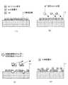
例えば、従来のALD法による窒化シリコン膜の成膜では、図4(1)に示すように、被成膜面11にシリコン原子Siを吸着させる工程を行う。次に、図4(2)に示すように、被成膜面11に窒素原子Nを供給して上記シリコン原子と窒素原子とを結合させて、原子層レベルのSi-N結合を形成し、窒化シリコン膜を形成する。このとき、Si-N結合と同時にSi-H、N-H結合が表層に形成することで最終的に膜中に水素を含有する。 For example, in the conventional film formation of a silicon nitride film by the ALD method, as shown in FIG. 4A, a step of adsorbing silicon atoms Si on the
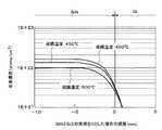
しかも、図5に示すように、窒化膜の成膜温度を低温化した場合、窒化膜中の水素含有量が増加することが分かっている。この水素は、Si-H、N-Hの結合によるものであり、この現象はALD法による窒化膜成膜時においても同様である。膜中の水素含有量が増えた場合、膜の耐熱性の低下、トランジスタ特性の低下(NBTI低下等)の問題を誘発することが懸念されおり、低温での窒化膜成膜による問題点となっている。 In addition, as shown in FIG. 5, it is known that when the deposition temperature of the nitride film is lowered, the hydrogen content in the nitride film increases. This hydrogen is due to the bond of Si—H and N—H, and this phenomenon is the same when the nitride film is formed by the ALD method. When the hydrogen content in the film increases, there is a concern that it may cause problems such as a decrease in heat resistance of the film and a decrease in transistor characteristics (such as a decrease in NBTI), which is a problem due to the formation of a nitride film at a low temperature. ing.
解決しようとする問題点は、窒化膜の成膜温度を低温(例えば500℃以下)化した場合、窒化膜中の水素含有量が増加する点である。 The problem to be solved is that when the deposition temperature of the nitride film is lowered (for example, 500 ° C. or lower), the hydrogen content in the nitride film increases.
本発明は、窒化膜の低温成膜において、成膜中に水素の除去工程を導入して、水素含有量を低減した窒化膜の提供を可能にすることを課題とする。 It is an object of the present invention to provide a nitride film having a reduced hydrogen content by introducing a hydrogen removal step during film formation of a nitride film at a low temperature.
請求項1に係る本発明は、原子層蒸着法により被成膜面に窒化シリコン膜を形成する工程を備えた半導体装置の製造方法であって、前記窒化シリコン膜の形成工程は、前記被成膜面にシリコン原子を吸着させる工程と、前記被成膜面に水活性化した水素を供給し、前記シリコン原子とともに吸着した水素原子に結合させて、前記被成膜面より前記水素を解離させる工程と、前記被成膜面に窒素原子を供給して前記シリコン原子と結合させて窒化シリコン膜を形成する工程とを備えたことを特徴とする。 The present invention according to
請求項1に係る本発明では、低温成膜が可能な原子層蒸着法により、被成膜面に水活性化した水素を供給し、シリコン原子とともに吸着した水素原子に結合させて、被成膜面より水素を解離させる工程を行った後、被成膜面に窒素原子を供給してシリコン原子と結合させて窒化シリコン膜を形成する工程を行うことから、水素原子の濃度を低減させた窒化シリコン膜の成膜が可能になる。 In the present invention according to
請求項3に係る本発明は、原子層蒸着法により被成膜面に窒化シリコン膜を形成する工程を備えた半導体装置の製造方法であって、前記窒化シリコン膜の形成工程は、前記被成膜面にシリコン原子を吸着させる工程と、前記被成膜面に窒素原子を供給して前記シリコン原子と結合させて窒化シリコン膜を形成する工程と、前記被成膜面に活性化した水素を供給し、前記被成膜面に吸着した水素原子に結合させて、前記被成膜面より前記水素を解離させる工程と、を備えたことを特徴とする。 The present invention according to
請求項3に係る本発明では、低温成膜が可能な原子層蒸着法により、被成膜面に窒素原子を供給してシリコン原子と結合させて窒化シリコン膜を形成する工程を行った後、被成膜面に活性化した水素を供給し、被成膜面に吸着した水素原子に結合させて、被成膜面より水素を解離させる工程を行うことから、窒化シリコン膜中の水素原子の濃度を低減させることが可能になる。 In the present invention according to
請求項1、3に係る本発明によれば、低温成膜による窒化膜中の水素の含有量を低減することができるので、窒化膜の耐熱性が高められる。例えばこの窒化膜をトランジスタのサイドウォールに適用した場合、成膜の低温化によるトランジスタ性能の改善、水素含有による電気特性劣化を防止が可能となる。 According to the first and third aspects of the present invention, the content of hydrogen in the nitride film formed by low-temperature film formation can be reduced, so that the heat resistance of the nitride film is improved. For example, when this nitride film is applied to a sidewall of a transistor, it is possible to improve transistor performance by lowering the film formation and to prevent deterioration of electrical characteristics due to hydrogen content.
請求項1に係る本発明の一実施の形態(第1実施例)を、図1の製造工程図によって説明する。 An embodiment (first example) of the present invention according to
第1実施例は、原子層蒸着法により被成膜面に窒化シリコン膜を形成する工程を備えた半導体装置の製造方法である。すなわち、上記窒化シリコン膜の形成工程は、シリコン(Si)原子を被成膜面に吸着させた後に活性化した水素(H)を導入し、を被成膜面に吸着していた水素と結合させ、除去する。その後、ラジカル化させた窒素により被成膜面に吸着させたシリコン(Si)を窒化させ、窒化膜を形成する。以下、具体的に説明する。 1st Example is a manufacturing method of the semiconductor device provided with the process of forming a silicon nitride film in the film-forming surface by atomic layer vapor deposition. That is, in the silicon nitride film formation step, activated hydrogen (H) is introduced after silicon (Si) atoms are adsorbed on the film formation surface, and bonded to the hydrogen adsorbed on the film formation surface. And remove. After that, silicon (Si) adsorbed on the film formation surface is nitrided by radicalized nitrogen to form a nitride film. This will be specifically described below.
図1(1)に示すように、被成膜面11にシリコン原子Siを吸着させる工程を行う。この工程では、被成膜面11にシリコン系ガスを供給することにより、シリコン原子Siを吸着させる。同時に水素原子Hや、上記シリコン系ガスに混入した原子、例えば塩素原子Clが吸着する。このときの成膜条件は、シリコン系ガスに例えばジクロロシラン(DCS:SiH2Cl2)を用い、成膜温度を500℃とした。ジクロロシランを用いたことにより、被成膜面11には、シリコン原子Si、水素原子H、塩素原子Clの各原子が吸着される。上記成膜温度は500℃としたが、例えば350℃〜600℃の範囲で、適宜決定することができる。As shown in FIG. 1A, a step of adsorbing silicon atoms Si on the
また、上記シリコン系ガスには、例えば、ジクロロシラン(DCS:SiH2Cl2)の他に、例えばトリクロロシラン(SiHCl3)を用いることができる。また、モノシラン(SiH4)、ジシラン(Si2H6)等のシラン系ガスを用いることも可能である。このシラン系ガスの場合、被成膜面11には、シリコン原子Siと水素原子Hが吸着することになる。For example, trichlorosilane (SiHCl3 ) can be used as the silicon-based gas, for example, in addition to dichlorosilane (DCS: SiH2 Cl2 ). It is also possible to use a silane-based gas such as monosilane (SiH4 ) or disilane (Si2 H6 ). In the case of this silane-based gas, silicon atoms Si and hydrogen atoms H are adsorbed on the
次に、図1(2)に示すように、被成膜面11に活性化した水素H*を供給する。例えば活性化した水素H*は、例えばラジカル化した水素を用いる。このとき、活性化した水素の供給量は、膜中の水素を増やすことがないように調節される必要がある。Next, as shown in FIG. 1B, activated hydrogen H* is supplied to the
次いで、図1(3)に示すように、上記シリコン原子Siとともに吸着した水素原子Hに、上記活性化した水素H*を結合させて、被成膜面11より上記水素Hを解離させる。Next, as shown in FIG. 1 (3), the activated hydrogen H* is bonded to the hydrogen atoms H adsorbed together with the silicon atoms Si, and the hydrogen H is dissociated from the
次に、図1(4)に示すように、被成膜面11に窒素原子Nを供給して上記シリコン原子と窒素とを結合させて、原子層レベルのSi-N結合を形成し、窒化シリコン膜を形成する。上記窒素原子Nには、例えばアンモニア(NH3)からラジカル化させた窒素ラジカルを用いる。この窒素ラジカルは活性化しているため、上記被成膜面11に吸着していたシリコン原子Siと結合して窒化シリコン膜を形成する。Next, as shown in FIG. 1 (4), nitrogen atoms N are supplied to the
そして、窒化シリコン膜が所望の膜厚になるまで、前記図1(1)〜(4)によって説明した上記被成膜面11にシリコン原子Siを吸着させる工程から上記被成膜面11に窒素原子Nを供給してシリコン原子Siと窒素原子Nとを結合させて窒化シリコン膜を形成する工程までを繰り返し行う。 Then, from the step of adsorbing silicon atoms Si to the
上記説明したように、原子層レベルで水素原子Hを除去するために、窒化前にラジカル(Radical)化した活性化な水素を流すことで、原子層表層の水素Hと反応させて、除去することができる。 As described above, in order to remove the hydrogen atoms H at the atomic layer level, the hydrogen atoms H are removed by reacting with the hydrogen H on the surface of the atomic layer by flowing an activated hydrogen radicalized before nitriding. be able to.
上記第1実施例では、低温成膜が可能な原子層蒸着法により、被成膜面11に水活性化した水素H*を供給し、シリコン原子Siとともに吸着した水素原子Hに結合させて、被成膜面11より水素Hを解離させる工程を行った後、被成膜面11に窒素原子Nを供給してシリコン原子Siと結合させて窒化シリコン膜を形成する工程を行うことから、水素原子の濃度を低減させた窒化シリコン膜の成膜が可能になる。このように、低温成膜による窒化膜中の水素の含有量を低減することができるので、窒化膜の耐熱性が高められる。例えばこの窒化膜をトランジスタのサイドウォール、サイドウォールスペーサ、ストレスライナー膜等に適用した場合、成膜の低温化によるトランジスタ性能の改善、水素含有による電気特性劣化を防止が可能となる。In the first embodiment, water-activated hydrogen H* is supplied to the
また、水素原子Hの解離時に、結合エネルギーにより表層が局所加熱されることも同時に期待できる。これによって、引っ張り(Tensile)側にストレスを上げることが可能となる。 It can also be expected that the surface layer is locally heated by the binding energy when the hydrogen atom H is dissociated. This makes it possible to increase the stress on the tensile side.
さらに、上記第1実施例の製造方法では、水素ラジカルにより塩素原子Clも除去することができる。塩素原子Clを除去することができるので、例えば、上記窒化膜をトランジスタのサイドウォール、サイドウォールスペーサ、ストレスライナー膜等に用いた場合、塩素原子によるトランジスタ特性の劣化を低減することができる。 Furthermore, in the manufacturing method of the first embodiment, chlorine atoms Cl can also be removed by hydrogen radicals. Since the chlorine atom Cl can be removed, for example, when the nitride film is used for a sidewall of a transistor, a sidewall spacer, a stress liner film, etc., deterioration of transistor characteristics due to chlorine atoms can be reduced.
次に、請求項2に係る本発明の一実施の形態(第2実施例)を、図2の製造工程図によって説明する。 Next, an embodiment (second example) of the present invention according to
図2(1)に示すように、被成膜面11にシリコン原子Siを吸着させる工程を行う。この工程では、被成膜面11にシリコン系ガスを供給することにより、シリコン原子Siを吸着させる。同時に水素原子Hや、上記シリコン系ガスに混入した原子、例えば塩素原子Clが吸着する。このときの成膜条件は、シリコン系ガスに例えばジクロロシラン(DCS:SiH2Cl2)を用い、成膜温度を500℃とした。ジクロロシランを用いたことにより、被成膜面11には、シリコン原子Si、水素原子H、塩素原子Clの各原子が吸着される。上記成膜温度は500℃としたが、例えば350℃〜600℃の範囲で、適宜決定することができる。As shown in FIG. 2A, a process of adsorbing silicon atoms Si on the
また、上記シリコン系ガスには、例えば、ジクロロシラン(DCS:SiH2Cl2)の他に、例えばトリクロロシラン(SiHCl3)を用いることができる。また、モノシラン(SiH4)、ジシラン(Si2H6)等のシラン系ガスを用いることも可能である。このシラン系ガスの場合、被成膜面11には、シリコン原子Siと水素原子Hが吸着することになる。For example, trichlorosilane (SiHCl3 ) can be used as the silicon-based gas, for example, in addition to dichlorosilane (DCS: SiH2 Cl2 ). It is also possible to use a silane-based gas such as monosilane (SiH4 ) or disilane (Si2 H6 ). In the case of this silane-based gas, silicon atoms Si and hydrogen atoms H are adsorbed on the
次に、図2(2)に示すように、被成膜面11に窒素原子Nを供給して上記シリコン原子と窒素とを結合させて、原子層レベルのSi-N結合を形成し、窒化シリコン膜を形成する。上記窒素原子Nには、例えばアンモニア(NH3)からラジカル化させた窒素ラジカルを用いる。この窒素ラジカルは活性化しているため、上記被成膜面11に吸着していたシリコン原子Siと結合して窒化シリコン膜を形成する。Next, as shown in FIG. 2 (2), nitrogen atoms N are supplied to the
次に、図2(3)に示すように、被成膜面11に活性化した水素H*を供給する。例えば活性化した水素H*は、例えばラジカル化した水素を用いる。このとき、活性化した水素の供給量は、膜中の水素を増やすことがないように調節される必要がある。Next, as shown in FIG. 2 (3), activated hydrogen H* is supplied to the
次いで、図2(4)に示すように、上記シリコン原子Siとともに吸着した水素原子Hに、上記活性化した水素H*を結合させて、被成膜面11より上記水素Hを解離させる。Next, as shown in FIG. 2 (4), the activated hydrogen H* is bonded to the hydrogen atoms H adsorbed together with the silicon atoms Si, and the hydrogen H is dissociated from the
そして、窒化シリコン膜が所望の膜厚になるまで、前記図2(1)〜(4)によって説明した上記被成膜面11にシリコン原子Siを吸着させる工程から上記活性化した水素H*を結合させて、被成膜面11より上記水素Hを解離させる工程までを繰り返し行う。Then, until the silicon nitride film has a desired thickness, the activated hydrogen H* is absorbed from the step of adsorbing silicon atoms Si on the
上記説明したように、原子層レベルで水素原子Hを除去するために、窒化後にラジカル(Radical)化した活性化な水素を流すことで、原子層表層の水素Hと反応させて、除去することができる。 As described above, in order to remove the hydrogen atom H at the atomic layer level, the active hydrogen that has been radicalized after nitridation is flowed to react with the hydrogen H on the surface layer of the atomic layer to remove it. Can do.
上記第2実施例では、低温成膜が可能な原子層蒸着法により、被成膜面11に水活性化した水素H*を供給し、シリコン原子Siとともに吸着した水素原子Hに結合させて、被成膜面11より水素Hを解離させる工程を行った後、被成膜面11に窒素原子Nを供給してシリコン原子Siと結合させて窒化シリコン膜を形成する工程を行うことから、水素原子の濃度を低減させた窒化シリコン膜の成膜が可能になる。このように、低温成膜による窒化膜中の水素の含有量を低減することができるので、窒化膜の耐熱性が高められる。例えばこの窒化膜をトランジスタのサイドウォール、サイドウォールスペーサ、ストレスライナー膜等に適用した場合、成膜の低温化によるトランジスタ性能の改善、水素含有による電気特性劣化を防止が可能となる。In the second embodiment, water-activated hydrogen H* is supplied to the
さらに、上記第2実施例では、窒化の際に用いるアンモニアの水素も除去することgはができるので、上記第1実施例で成膜される窒化膜よりも水素をより多く除去することが可能になるという利点もある。 Furthermore, in the second embodiment, since hydrogen of ammonia used for nitriding can be removed, more hydrogen can be removed than the nitride film formed in the first embodiment. There is also an advantage of becoming.
また、水素原子Hの解離時に、結合エネルギーにより表層が局所加熱されることも同時に期待できる。これによって、引っ張り(Tensile)側にストレスを上げることが可能となる。 It can also be expected that the surface layer is locally heated by the binding energy when the hydrogen atom H is dissociated. This makes it possible to increase the stress on the tensile side.
さらに、上記第2実施例の製造方法では、水素ラジカルにより塩素原子Clも除去することができる。塩素原子Clを除去することができるので、例えば、上記窒化膜をトランジスタのサイドウォール、サイドウォールスペーサ、ストレスライナー膜等に用いた場合、塩素原子によるトランジスタ特性の劣化を低減することができる。 Furthermore, in the manufacturing method of the second embodiment, chlorine atoms Cl can also be removed by hydrogen radicals. Since the chlorine atom Cl can be removed, for example, when the nitride film is used for a sidewall of a transistor, a sidewall spacer, a stress liner film, etc., deterioration of transistor characteristics due to chlorine atoms can be reduced.
さらに、上記各実施例は、例えば、窒化シリコン膜の成膜に適用できるが、金属窒化膜の成膜にも適用できる。この場合、原料ガスに有機金属ガス、例えば金属アルコキシドガスを用いる。通常、金属アルコキシドには水素が含まれているため、水素の除去に上記各実施例で説明した製造方法が有効となる。 Further, each of the above embodiments can be applied to the formation of a silicon nitride film, for example, but can be applied to the formation of a metal nitride film. In this case, an organic metal gas such as a metal alkoxide gas is used as the source gas. Usually, since the metal alkoxide contains hydrogen, the production methods described in the above embodiments are effective for removing hydrogen.
上記各実施例で説明した製造方法では、トランジスタのゲート電極に形成されるサイドウォール膜に対して適用することができる。その一例を図3の概略構成断面図によって説明する。 The manufacturing methods described in the above embodiments can be applied to the sidewall film formed on the gate electrode of the transistor. An example of this will be described with reference to the schematic sectional view of FIG.
例えば、図3に示すように、半導体基板21上にゲート絶縁膜22を介してゲート電極23が形成されている。このゲート電極23上にはオフセット絶縁膜24が形成されている。またげ23の両側にはオフセットスペーサ25を介してサイドウォール26が形成され、さらに上記オフセット絶縁膜24、サイドウォール26等を被覆するように、半導体基板21上にストレスライナー膜31が形成されている。例えば、上記オフセットスペーサ25、サイドウォール26、ストレスライナー膜31は、上記第1実施例もしくは第2実施例で説明した製造方法による窒化膜を用いることができる。この場合の窒化膜は、例えば窒化シリコン膜を用いる。さらに、上記ゲート電極23の両側における半導体基板21にはソース・ドレイン領域27、28が形成されている。 For example, as shown in FIG. 3, the
本発明の製造方法を適用することによって、低温成膜によりサイドウォール26を形成するための窒化膜を成膜することができ、かつ窒化膜の膜質改善が図れるので、トランジスタ特性(例えば、NBTI(Negative Bias Temperature Instability)特性)を向上させることができる。また、上記サイドウォール26と同様に、オフセットスペーサー25やストレスライナー膜31の成膜に対して本発明の製造方法を適用することにより、低温成膜による窒化膜の膜質改善によるトランジスタ特性の向上が達成される。 By applying the manufacturing method of the present invention, a nitride film for forming the
11…被成膜面、Si…シリコン原子、H…水素原子、H*…活性化した水素、N…窒素原子11 ... deposition surface, Si ... silicon atom, H ... hydrogen atom, H* ... activated hydrogen, N ... nitrogen atom
Claims (4)
Translated fromJapanese前記窒化シリコン膜の形成工程は、
前記被成膜面にシリコン原子を吸着させる工程と、
前記被成膜面に活性化した水素を供給し、前記シリコン原子とともに吸着した水素原子に結合させて、前記被成膜面より前記水素を解離させる工程と、
前記被成膜面に窒素原子を供給して前記シリコン原子と結合させて窒化シリコン膜を形成する工程と
を備えたことを特徴とする半導体装置の製造方法。A method for manufacturing a semiconductor device comprising a step of forming a silicon nitride film on a deposition surface by atomic layer deposition,
The step of forming the silicon nitride film includes
Adsorbing silicon atoms on the deposition surface;
Supplying activated hydrogen to the film formation surface, bonding to hydrogen atoms adsorbed together with the silicon atoms, and dissociating the hydrogen from the film formation surface;
And a step of supplying a nitrogen atom to the deposition surface and bonding the nitrogen atom to the silicon atom to form a silicon nitride film.
前記被成膜面にシリコン原子を吸着させる工程から前記被成膜面に窒素原子を供給して前記シリコン原子と窒素原子とを結合させて窒化シリコン膜を形成する工程までを繰り返し行う
ことを特徴とする請求項1記載の半導体装置の製造方法。The step of forming the silicon nitride film includes
The process from the step of adsorbing silicon atoms to the film formation surface to the step of forming a silicon nitride film by supplying nitrogen atoms to the film formation surface and combining the silicon atoms and nitrogen atoms is repeated. A method for manufacturing a semiconductor device according to claim 1.
前記窒化シリコン膜の形成工程は、
前記被成膜面にシリコン原子を吸着させる工程と、
前記被成膜面に窒素原子を供給して前記シリコン原子と結合させて窒化シリコン膜を形成する工程と、
前記被成膜面に活性化した水素を供給し、前記被成膜面に吸着した水素原子に結合させて、前記被成膜面より前記水素を解離させる工程と、
を備えたことを特徴とする半導体装置の製造方法。A method for manufacturing a semiconductor device comprising a step of forming a silicon nitride film on a deposition surface by atomic layer deposition,
The step of forming the silicon nitride film includes
Adsorbing silicon atoms on the deposition surface;
Supplying nitrogen atoms to the deposition surface and combining with the silicon atoms to form a silicon nitride film;
Supplying activated hydrogen to the film formation surface, bonding to hydrogen atoms adsorbed on the film formation surface, and dissociating the hydrogen from the film formation surface;
A method for manufacturing a semiconductor device, comprising:
前記被成膜面にシリコン原子を吸着させる工程から前記被成膜面に活性化した水素を供給し、前記被成膜面に吸着した水素原子に結合させて、前記被成膜面より前記水素を解離させる工程までを繰り返し行う
ことを特徴とする請求項3記載の半導体装置の製造方法。The step of forming the silicon nitride film includes
The activated hydrogen is supplied to the film formation surface from the step of adsorbing silicon atoms on the film formation surface, and is bonded to the hydrogen atoms adsorbed on the film formation surface, so that the hydrogen is supplied from the film formation surface. The method for manufacturing a semiconductor device according to claim 3, wherein the steps up to the step of dissociating are repeated.
Priority Applications (1)
| Application Number | Priority Date | Filing Date | Title |
|---|---|---|---|
| JP2007053704AJP2008218684A (en) | 2007-03-05 | 2007-03-05 | Method of fabricating semiconductor device |
Applications Claiming Priority (1)
| Application Number | Priority Date | Filing Date | Title |
|---|---|---|---|
| JP2007053704AJP2008218684A (en) | 2007-03-05 | 2007-03-05 | Method of fabricating semiconductor device |
Publications (1)
| Publication Number | Publication Date |
|---|---|
| JP2008218684Atrue JP2008218684A (en) | 2008-09-18 |
Family
ID=39838376
Family Applications (1)
| Application Number | Title | Priority Date | Filing Date |
|---|---|---|---|
| JP2007053704APendingJP2008218684A (en) | 2007-03-05 | 2007-03-05 | Method of fabricating semiconductor device |
Country Status (1)
| Country | Link |
|---|---|
| JP (1) | JP2008218684A (en) |
Cited By (24)
| Publication number | Priority date | Publication date | Assignee | Title |
|---|---|---|---|---|
| WO2012047812A3 (en)* | 2010-10-04 | 2012-09-27 | Applied Materials, Inc. | Atomic layer deposition of silicon nitride using dual-source precursor and interleaved plasma |
| US8329262B2 (en) | 2010-01-05 | 2012-12-11 | Applied Materials, Inc. | Dielectric film formation using inert gas excitation |
| US8357435B2 (en) | 2008-05-09 | 2013-01-22 | Applied Materials, Inc. | Flowable dielectric equipment and processes |
| WO2013039866A3 (en)* | 2011-09-13 | 2013-05-10 | Applied Materials, Inc. | Activated silicon precursors for low temperature deposition |
| US8445078B2 (en) | 2011-04-20 | 2013-05-21 | Applied Materials, Inc. | Low temperature silicon oxide conversion |
| US8450191B2 (en) | 2011-01-24 | 2013-05-28 | Applied Materials, Inc. | Polysilicon films by HDP-CVD |
| US8449942B2 (en) | 2009-11-12 | 2013-05-28 | Applied Materials, Inc. | Methods of curing non-carbon flowable CVD films |
| US8466073B2 (en) | 2011-06-03 | 2013-06-18 | Applied Materials, Inc. | Capping layer for reduced outgassing |
| US8551891B2 (en) | 2011-10-04 | 2013-10-08 | Applied Materials, Inc. | Remote plasma burn-in |
| US8563445B2 (en) | 2010-03-05 | 2013-10-22 | Applied Materials, Inc. | Conformal layers by radical-component CVD |
| US8617989B2 (en) | 2011-09-26 | 2013-12-31 | Applied Materials, Inc. | Liner property improvement |
| US8629067B2 (en) | 2009-12-30 | 2014-01-14 | Applied Materials, Inc. | Dielectric film growth with radicals produced using flexible nitrogen/hydrogen ratio |
| US8647992B2 (en) | 2010-01-06 | 2014-02-11 | Applied Materials, Inc. | Flowable dielectric using oxide liner |
| US8664127B2 (en) | 2010-10-15 | 2014-03-04 | Applied Materials, Inc. | Two silicon-containing precursors for gapfill enhancing dielectric liner |
| US8716154B2 (en) | 2011-03-04 | 2014-05-06 | Applied Materials, Inc. | Reduced pattern loading using silicon oxide multi-layers |
| US8741788B2 (en) | 2009-08-06 | 2014-06-03 | Applied Materials, Inc. | Formation of silicon oxide using non-carbon flowable CVD processes |
| US8889566B2 (en) | 2012-09-11 | 2014-11-18 | Applied Materials, Inc. | Low cost flowable dielectric films |
| US8980382B2 (en) | 2009-12-02 | 2015-03-17 | Applied Materials, Inc. | Oxygen-doping for non-carbon radical-component CVD films |
| US9018108B2 (en) | 2013-01-25 | 2015-04-28 | Applied Materials, Inc. | Low shrinkage dielectric films |
| US9285168B2 (en) | 2010-10-05 | 2016-03-15 | Applied Materials, Inc. | Module for ozone cure and post-cure moisture treatment |
| US9343317B2 (en) | 2013-07-01 | 2016-05-17 | Micron Technology, Inc. | Methods of forming silicon-containing dielectric materials and semiconductor device structures |
| US9404178B2 (en) | 2011-07-15 | 2016-08-02 | Applied Materials, Inc. | Surface treatment and deposition for reduced outgassing |
| US9412581B2 (en) | 2014-07-16 | 2016-08-09 | Applied Materials, Inc. | Low-K dielectric gapfill by flowable deposition |
| US10283321B2 (en) | 2011-01-18 | 2019-05-07 | Applied Materials, Inc. | Semiconductor processing system and methods using capacitively coupled plasma |
- 2007
- 2007-03-05JPJP2007053704Apatent/JP2008218684A/enactivePending
Cited By (28)
| Publication number | Priority date | Publication date | Assignee | Title |
|---|---|---|---|---|
| US8357435B2 (en) | 2008-05-09 | 2013-01-22 | Applied Materials, Inc. | Flowable dielectric equipment and processes |
| US8741788B2 (en) | 2009-08-06 | 2014-06-03 | Applied Materials, Inc. | Formation of silicon oxide using non-carbon flowable CVD processes |
| US8449942B2 (en) | 2009-11-12 | 2013-05-28 | Applied Materials, Inc. | Methods of curing non-carbon flowable CVD films |
| US8980382B2 (en) | 2009-12-02 | 2015-03-17 | Applied Materials, Inc. | Oxygen-doping for non-carbon radical-component CVD films |
| US8629067B2 (en) | 2009-12-30 | 2014-01-14 | Applied Materials, Inc. | Dielectric film growth with radicals produced using flexible nitrogen/hydrogen ratio |
| US8329262B2 (en) | 2010-01-05 | 2012-12-11 | Applied Materials, Inc. | Dielectric film formation using inert gas excitation |
| US8647992B2 (en) | 2010-01-06 | 2014-02-11 | Applied Materials, Inc. | Flowable dielectric using oxide liner |
| US8563445B2 (en) | 2010-03-05 | 2013-10-22 | Applied Materials, Inc. | Conformal layers by radical-component CVD |
| WO2012047812A3 (en)* | 2010-10-04 | 2012-09-27 | Applied Materials, Inc. | Atomic layer deposition of silicon nitride using dual-source precursor and interleaved plasma |
| US9285168B2 (en) | 2010-10-05 | 2016-03-15 | Applied Materials, Inc. | Module for ozone cure and post-cure moisture treatment |
| US8664127B2 (en) | 2010-10-15 | 2014-03-04 | Applied Materials, Inc. | Two silicon-containing precursors for gapfill enhancing dielectric liner |
| US10283321B2 (en) | 2011-01-18 | 2019-05-07 | Applied Materials, Inc. | Semiconductor processing system and methods using capacitively coupled plasma |
| US8450191B2 (en) | 2011-01-24 | 2013-05-28 | Applied Materials, Inc. | Polysilicon films by HDP-CVD |
| US8716154B2 (en) | 2011-03-04 | 2014-05-06 | Applied Materials, Inc. | Reduced pattern loading using silicon oxide multi-layers |
| US8445078B2 (en) | 2011-04-20 | 2013-05-21 | Applied Materials, Inc. | Low temperature silicon oxide conversion |
| US8466073B2 (en) | 2011-06-03 | 2013-06-18 | Applied Materials, Inc. | Capping layer for reduced outgassing |
| US9404178B2 (en) | 2011-07-15 | 2016-08-02 | Applied Materials, Inc. | Surface treatment and deposition for reduced outgassing |
| US8821986B2 (en) | 2011-09-13 | 2014-09-02 | Applied Materials, Inc. | Activated silicon precursors for low temperature deposition |
| WO2013039866A3 (en)* | 2011-09-13 | 2013-05-10 | Applied Materials, Inc. | Activated silicon precursors for low temperature deposition |
| US8617989B2 (en) | 2011-09-26 | 2013-12-31 | Applied Materials, Inc. | Liner property improvement |
| US8551891B2 (en) | 2011-10-04 | 2013-10-08 | Applied Materials, Inc. | Remote plasma burn-in |
| US8889566B2 (en) | 2012-09-11 | 2014-11-18 | Applied Materials, Inc. | Low cost flowable dielectric films |
| US9018108B2 (en) | 2013-01-25 | 2015-04-28 | Applied Materials, Inc. | Low shrinkage dielectric films |
| US9343317B2 (en) | 2013-07-01 | 2016-05-17 | Micron Technology, Inc. | Methods of forming silicon-containing dielectric materials and semiconductor device structures |
| US10121966B2 (en) | 2013-07-01 | 2018-11-06 | Micron Technology, Inc. | Semiconductor device structures including silicon-containing dielectric materials |
| US10468595B2 (en) | 2013-07-01 | 2019-11-05 | Micron Technology, Inc. | Semiconductor device structures including silicon-containing dielectric materials |
| US10930846B2 (en) | 2013-07-01 | 2021-02-23 | Micron Technology, Inc. | Methods of forming silicon-containing dielectric materials and methods of forming a semiconductor device comprising nitrogen radicals and oxygen-containing, silicon-containing, or carbon-containing precursors |
| US9412581B2 (en) | 2014-07-16 | 2016-08-09 | Applied Materials, Inc. | Low-K dielectric gapfill by flowable deposition |
Similar Documents
| Publication | Publication Date | Title |
|---|---|---|
| JP2008218684A (en) | Method of fabricating semiconductor device | |
| KR100660890B1 (en) | Silicon dioxide film formation method using ALD | |
| JP5829196B2 (en) | Method for forming silicon oxide film | |
| JP5145672B2 (en) | Manufacturing method of semiconductor device | |
| TWI728941B (en) | METHOD OF FORMING SiN THIN FILM ON SURFACE OF SUBSTRATE IN REACTION SPACE | |
| US7351670B2 (en) | Method for producing silicon nitride films and process for fabricating semiconductor devices using said method | |
| JP2776726B2 (en) | Method for manufacturing semiconductor device | |
| JP4279176B2 (en) | Method for forming silicon nitride film | |
| US20120220139A1 (en) | Method of depositing dielectric film by modified peald method | |
| TWI866642B (en) | Method to enhance growth rate for selective epitaxial growth | |
| JP2014527315A (en) | Non-reactive dry removal process for semiconductor integration | |
| JP2012195564A (en) | Semiconductor device manufacturing method, substrate processing method, substrate processing apparatus, and program | |
| CN1881541A (en) | Film formation method and apparatus for semiconductor process | |
| JP2005310927A (en) | Deposition method of high quality silicon nitride film by ultraviolet irradiation | |
| KR20250026878A (en) | Methods for forming films containing silicon boron with low leakage current | |
| JP2008508721A (en) | Deposition of thin tungsten silicide layers and gate metal incorporation | |
| TW565893B (en) | Semiconductor device and method for producing the same | |
| JP5378287B2 (en) | Manufacturing method of semiconductor device | |
| JP4876375B2 (en) | Semiconductor device and manufacturing method thereof | |
| US7026226B1 (en) | Method of hydrogenating a poly-silicon layer | |
| JP4139266B2 (en) | Method for manufacturing a memory element for a semiconductor memory | |
| JP5199954B2 (en) | Manufacturing method of semiconductor device | |
| WO2021241449A1 (en) | Semiconductor device | |
| JP4635062B2 (en) | Manufacturing method of semiconductor device | |
| CN116536645A (en) | Semiconductor substrate and method for manufacturing the same |