JP2008218516A - Pattern evaluation method, evaluation mark, and semiconductor device manufacturing method using the same - Google Patents
Pattern evaluation method, evaluation mark, and semiconductor device manufacturing method using the sameDownload PDFInfo
- Publication number
- JP2008218516A JP2008218516AJP2007050436AJP2007050436AJP2008218516AJP 2008218516 AJP2008218516 AJP 2008218516AJP 2007050436 AJP2007050436 AJP 2007050436AJP 2007050436 AJP2007050436 AJP 2007050436AJP 2008218516 AJP2008218516 AJP 2008218516A
- Authority
- JP
- Japan
- Prior art keywords
- pattern
- mask
- mark
- insulating film
- sidewall insulating
- Prior art date
- Legal status (The legal status is an assumption and is not a legal conclusion. Google has not performed a legal analysis and makes no representation as to the accuracy of the status listed.)
- Pending
Links
Images


Landscapes
- Testing Or Measuring Of Semiconductors Or The Like (AREA)
- Internal Circuitry In Semiconductor Integrated Circuit Devices (AREA)
Abstract
Translated fromJapaneseDescription
Translated fromJapanese本発明は、微細パターンの評価方法、その評価マーク、それを用いた半導体装置の製造方法に関する。 The present invention relates to a method for evaluating a fine pattern, its evaluation mark, and a method for manufacturing a semiconductor device using the same.
半導体装置の微細化は、リソグラフィ技術に大きく依存する。そのため、リソグラフィの解像限界を超える微細な幅を有するラインアンドスペースパターンを形成することは、一般的には困難である。このような問題に対して、解像限界を超える微細パターンの形成方法として、所謂側壁残し法と呼ばれる方法が提案されている(例えば、特許文献1、図1〜図3参照)。 The miniaturization of a semiconductor device greatly depends on lithography technology. Therefore, it is generally difficult to form a line and space pattern having a fine width exceeding the resolution limit of lithography. In order to solve such a problem, a so-called side wall leaving method has been proposed as a method for forming a fine pattern exceeding the resolution limit (see, for example,
この技術は、例えば、配線層上にレジスト等を用いたリソグラフィでダミーパターンを形成し、このダミーパターンを覆う絶縁膜を形成後、RIE等の異方性エッチングを行なう。これによりダミーパターンの側壁に側壁絶縁膜を残存させ、その後ダミーパターンを除去する。残置された側壁絶縁膜をマスクとして配線層をエッチングすることにより、微細配線パターンが形成される。 In this technique, for example, a dummy pattern is formed on a wiring layer by lithography using a resist, and after forming an insulating film covering the dummy pattern, anisotropic etching such as RIE is performed. As a result, the sidewall insulating film is left on the sidewall of the dummy pattern, and then the dummy pattern is removed. A fine wiring pattern is formed by etching the wiring layer using the left side wall insulating film as a mask.
上記の方法によって、微細化パターンを形成することはできるが、例えば、レジストパターンの寸法誤差や、マスクである側壁絶縁膜の形状に依存する下地配線層のエッチングレートのばらつきに起因して、形成されたラインアンドスペースパターンの寸法が1個おきに変化する現象が発生する。 A fine pattern can be formed by the above method, but it is formed due to variations in the etching rate of the underlying wiring layer depending on the dimensional error of the resist pattern and the shape of the sidewall insulating film that is a mask, for example. A phenomenon occurs in which the dimension of the line and space pattern is changed every other line.
上記の如き誤差の影響を簡単に短時間で計測し、その結果をプロセスにフィードバックすることによって、側壁残しプロセスの品質を改善する必要がある。このような目的のために、パターンを走査型電子顕微鏡(SEM)を用いて検査することもできるが、SEMの計測は一般的に時間がかかるので、基板内の多数の点に関する情報を収集するには不向きである。
本発明は、上記の如き状況に鑑みて為されたもので、SEMを用いるよりもより簡単に、側壁残しプロセスの不具合に起因する寸法誤差を測定・評価する方法と、その評価マーク、それを用いた半導体装置の製造方法を提供することを目的とする。 The present invention has been made in view of the above situation, and more easily than using an SEM, a method for measuring and evaluating a dimensional error caused by a defect in a sidewall leaving process, an evaluation mark thereof, It is an object of the present invention to provide a method for manufacturing a used semiconductor device.
上記課題を解決するために、本発明のパターン評価方法は、第1の下地膜が第2の下地膜の上面に形成された半導体基板を準備する工程と、前記半導体基板にレジストを塗布し、所定のパターンを成すように露光する工程と、前記露光された半導体基板を現像してレジストマスクを形成する工程と、前記レジストマスクを用いて、前記第1の下地膜をエッチングしてダミーパターンを形成する工程と、前記ダミーパターンに側壁絶縁膜を形成する工程と、前記側壁絶縁膜形成後に、前記ダミーパターンを除去する工程と、
前記側壁絶縁膜を用いて前記第2の下地膜をエッチングして、パターン評価用マークを形成し評価する工程とを具備し、前記ダミーパターンに側壁絶縁膜を形成する工程は、前記側壁絶縁膜は湾曲面と垂直面とからなる断面形状を有し、第1の方向に前記湾曲面がある少なくとも1対の第1の側壁絶縁膜と、前記第1の方向と逆向きの第2の方向に前記湾曲面がある少なくとも1対の第2の側壁絶縁膜を、前記ダミーパターンの側壁に形成する工程を含み、前記ダミーパターンを除去する工程は、前記ダミーパターンを除去して、夫々が一対の前記第1及び第2の側壁絶縁膜を前記第2の下地膜上に残置する工程を含み、前記側壁絶縁膜を用いて前記第2の下地膜をエッチングして、パターン評価用マークを形成し評価する工程は、前記第1の側壁絶縁膜から形成された第1のマスクと、前記第2の側壁絶縁膜から形成された第2のマスクを用いて前記第2の下地膜をエッチングし、前記第2の下地膜に、前記第1のマスクに対応して形成された第1のマークと、前記第2のマスクに対応して形成された第2のマークとを形成するサブ工程と、前記第1及び第2のマスク、あるいは前記第1及び第2のマークに関して、その相対位置を計測し、夫々の基準位置からのずれを評価するサブ工程とを具備することを特徴とする。In order to solve the above problems, a pattern evaluation method of the present invention includes a step of preparing a semiconductor substrate in which a first base film is formed on an upper surface of a second base film, A step of exposing to form a predetermined pattern; a step of developing the exposed semiconductor substrate to form a resist mask; and etching the first base film using the resist mask to form a dummy pattern Forming a sidewall insulating film on the dummy pattern, removing the dummy pattern after the sidewallinsulating film is formed,
Etching the second base film using the sidewall insulating film to form and evaluate a pattern evaluation mark, and the step of forming the sidewall insulating film on the dummy pattern includes the sidewall insulating film Has a cross-sectional shape composed of a curved surface and a vertical surface, at least a pair of first sidewall insulating films having the curved surface in a first direction, and a second direction opposite to the first direction. Forming at least one pair of second side wall insulating films having the curved surfaces on the side walls of the dummy pattern, and the step of removing the dummy pattern includes removing the dummy pattern and each pair A step of leaving the first and second side wall insulating films on the second base film, and forming the pattern evaluation mark by etching the second base film using the side wall insulating film. And evaluating the first step Etching the second base film using a first mask formed from a sidewall insulating film and a second mask formed from the second sidewall insulating film, A sub-process for forming a first mark formed corresponding to the first mask and a second mark formed corresponding to the second mask; the first and second masks; Alternatively, the method includes a sub-process for measuring the relative positions of the first and second marks and evaluating deviations from the respective reference positions.
また、本発明のパターン評価用マークは、垂直面から成る第1の側面と、湾曲面から成り前記第1の側面に平行する第2の側面とを有する第1の直線パターンが対を成す第1のマークと、前記第1の直線パターンの前記第2の側面に対向しつつ平行する湾曲面からなる第3の側面と、垂直面からなり前記第3の側面に平行する第4の側面を有する第2の直線パターンが対を成す第2のマークとを具備することを特徴とする。 In the pattern evaluation mark of the present invention, a first linear pattern having a first side surface composed of a vertical surface and a second side surface composed of a curved surface and parallel to the first side surface forms a pair. A first side surface, a third side surface composed of a curved surface parallel to the second side surface of the first linear pattern, and a fourth side surface composed of a vertical surface and parallel to the third side surface. The second linear pattern having a second mark that forms a pair.
また、本発明の半導体装置の製造方法は、第1の下地膜が第2の下地膜の上面に形成された半導体基板を準備する工程と、前記半導体基板にレジストを塗布し、所定のパターンを成すように露光する工程と、前記露光された半導体基板を現像してレジストマスクを形成する工程と、前記レジストマスクに対して、スリミングを実施する選択的な工程と、前記現像若しくはさらにスリミングされたレジストマスクを用いて、前記第1の下地膜をエッチングしてダミーパターンを形成する工程と、前記ダミーパターンに側壁膜を形成する工程と、前記側壁膜形成後に、前記ダミーパターンを除去する工程と、前記側壁絶縁膜を用いて前記第2の下地膜をエッチングして、パターン評価用マスクを形成する工程と、前記パターン評価用マスクを用いて、第2の下地膜をエッチングして、前記パターン評価用マスクに対応したパターン評価用マークを形成する工程と、前記パターン評価用マーク計測して補正の要否を判定し、補正が必要な場合は、前記露光工程、若しくは前記スリミング工程、若しくは前記第1の下地膜のエッチング工程に補正値をフィードバックする工程を具備し、前記パターン評価用マスクは、垂直面から成る第1の側面と、湾曲面から成り前記第1の側面に平行する第2の側面とを有する第1の直線パターンが対を成す第1のマスクと、前記第1の直線パターンの前記第2の側面に対向しつつ平行する湾曲面からなる第3の側面と、垂直面からなり前記第3の側面に平行する第4の側面を有する第2の直線パターンが対を成す第2のマスクとを具備することを特徴とする。 According to another aspect of the present invention, there is provided a method for manufacturing a semiconductor device, comprising: preparing a semiconductor substrate having a first base film formed on an upper surface of a second base film; applying a resist to the semiconductor substrate; Exposing the exposed semiconductor substrate to form a resist mask, selectively performing slimming on the resist mask, and developing or further slimming. Etching the first base film using a resist mask to form a dummy pattern; forming a sidewall film on the dummy pattern; removing the dummy pattern after the sidewall film is formed; Etching the second base film using the sidewall insulating film to form a pattern evaluation mask, and using the pattern evaluation mask A step of etching the second base film to form a pattern evaluation mark corresponding to the pattern evaluation mask, and measuring the pattern evaluation mark to determine whether or not correction is necessary. Comprises a step of feeding back a correction value to the exposure step, the slimming step, or the etching step of the first underlayer, wherein the pattern evaluation mask has a first side surface formed of a vertical surface, and a curved surface. A first mask having a pair of first linear patterns, each having a second side surface parallel to the first side surface, and parallel to the second side surface of the first linear pattern. And a second mask having a pair of second linear patterns each having a fourth side surface formed of a vertical surface and parallel to the third side surface. That.
本発明によれば、SEMを用いるよりもはるかに簡単に、側壁残しプロセスの不具合に起因する寸法誤差を測定・評価することができる。本発明のパターン評価用マーク、パターン評価方法を用いて、半導体装置を製造すれば、効率の良いプロセスを確立することが可能になる。 According to the present invention, it is possible to measure and evaluate a dimensional error caused by a defect in a sidewall leaving process much more easily than using an SEM. If a semiconductor device is manufactured using the pattern evaluation mark and the pattern evaluation method of the present invention, an efficient process can be established.
本発明の実施形態を説明する前に、側壁残しプロセスにおけるラインアンドスペース寸法にばらつきが生じるメカニズムについて説明する。ラインアンドスペースパターンは、一般にレジストパターンを用いて被加工膜をエッチング加工するが、レジスト露光時のドーズ量によって、パターン寸法が変化する。また、スリミング技術を用いてマスク寸法を小さくする場合においても、寸法が変動する要因を含む。さらに、エッチング量(時間)によっても寸法が変動する。このような場合、簡易に寸法ばらつきを検査する方法があれば、工程条件に速やかにフィードバックすることができ、高歩留りで製造を行なうことが可能になる。 Before describing the embodiment of the present invention, a mechanism that causes variations in line and space dimensions in the sidewall leaving process will be described. In the line and space pattern, a film to be processed is generally etched using a resist pattern, but the pattern dimension changes depending on the dose during resist exposure. Further, even when the mask dimension is reduced by using the slimming technique, a factor that causes the dimension variation is included. Furthermore, the dimensions vary depending on the etching amount (time). In such a case, if there is a simple method for inspecting the dimensional variation, it is possible to promptly feed back to the process conditions and manufacture can be performed with a high yield.
図33は、一般的な側壁残しプロセスと、寸法変動が生じるメカニズムを摸式的に示した図である。図において、1は半導体基板、2は配線層、3は絶縁膜、4はレジストパターンである。等間隔tのラインアンドスペースパターンを製作する場合、レジストパターン4の幅はt、間隔は3tとする(図33(a))。この時、レジストパターン4の幅がTに変動した場合を図33(a´)に示す。 FIG. 33 is a diagram schematically showing a general sidewall leaving process and a mechanism in which dimensional variation occurs. In the figure, 1 is a semiconductor substrate, 2 is a wiring layer, 3 is an insulating film, and 4 is a resist pattern. When a line and space pattern with equal intervals t is manufactured, the width of the
このレジストパターン4を用いて、絶縁層3をRIE等を用いて異方性エッチングした結果を図33(b)、(b´)に示す。ここで得られたパターンに対して、絶縁膜(不図示)をコートし、RIEを行なうことにより、側壁絶縁膜5を得る。この側壁絶縁膜の配線層2と接する面における幅は、tとなるように条件を調整する(図33(c)、(c´))。 33B and 33B show the result of anisotropic etching of the insulating
続いて絶縁膜パターン3を除去すると、図33(d)、(d´)のように、側壁絶縁膜5のみが残置される。この側壁絶縁膜5を用いて配線層2に対してRIEを行なうと、図33(e)では、ラインアンドスペース寸法がtの配線パターンが得られる。一方、図31(e´)では、ライン寸法はtであるが、スペース寸法が交互にT、t´(<T)となる。 Subsequently, when the
本発明のパターン評価方法では、上記の如き寸法変化を容易に検出することができる。以下、本発明の実施形態を説明する。
(第1の実施形態)
図1は、第1の実施形態に係る評価パターン(ダミーパターン)の上面図である。幅広パターン101と、例えばラインアンドスペース(L/S)64nmの微細パターン102、三角パターン103の組み合わせになっている。図面の左、及び上に配置されたブロック100aでは、幅広パターン101を微細パターン102が、64nmの間隔を開けて挟んで形成されている。図面の右側及び下側のブロック100bにおいては、101と102の間隔、及び102と103の間隔は64nmに設定されている。パターンの長さは、例えば20nmである。なお、三角パターンは必ずしも三角である必要は無く、直交する二辺が存在すればよく、方形にならない範囲で斜辺を変化させることができる。In the pattern evaluation method of the present invention, the dimensional change as described above can be easily detected. Embodiments of the present invention will be described below.
(First embodiment)
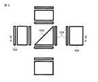
FIG. 1 is a top view of an evaluation pattern (dummy pattern) according to the first embodiment. A
評価方法としては、先ず図1に示すように、半導体基板(例えば、シリコン基板)1上に、第1の下地層としての配線層(例えば、Al,Cu層)2、第2の下地層としての絶縁層(例えば、シリコン酸化膜)3を順次形成する。次いで、レジストパターン101〜103を、絶縁層3の上に形成する。図2は、図1のA−A´線に相当する断面図である。このレジストパターンを101〜103をマスクとして第2の下地層を異方性エッチングして絶縁層3よりなるダミーパターンを形成する。 As an evaluation method, first, as shown in FIG. 1, on a semiconductor substrate (for example, a silicon substrate) 1, a wiring layer (for example, Al, Cu layer) 2 as a first foundation layer, and as a second foundation layer. Insulating layers (for example, silicon oxide films) 3 are sequentially formed. Next,
続いて、周知の側壁残し法を適用して、図3のように絶縁層3よりなるダミーパターンの側面に側壁絶縁膜104を形成する。側壁絶縁膜としては、例えばシリコン窒化膜が使用される。このときの、A−A´線に沿った断面図を図4に示す。後の説明において理解が容易なように、右側の側壁絶縁膜は黒く塗りつぶし、左側の絶縁膜は白抜きで表示している。 Subsequently, the
さらに図5のように絶縁層3を剥離し、側壁絶縁膜104を残す。さらに基板全面にレジストを塗布して露光を行い、図7及び図8のようにレジストパターン105を形成した後、側壁絶縁膜104の露出部分をエッチングにより取り除く。さらにレジスト105を剥離すると図9に示された側壁パターンが基板上に残る。図6.8、10は、夫々図5、7、9のA−A´線に沿った断面図である。 Further, as shown in FIG. 5, the insulating
ここで注目すべきは、図1に示すような評価パターン(ダミーパターン)を用いて、その側壁に側壁絶縁膜を形成し、不要部分を除去すると、図9及び図10に示すような側壁絶縁膜104からなるマスクが形成されることである。即ち、側壁絶縁膜(マスク)104は湾曲面と垂直面とからなる断面形状を有し、ダミーパターンに側壁絶縁膜を形成する工程は、第1の方向に湾曲面がある少なくとも1対の第1の側壁絶縁膜と、第1の方向と逆の第2の方向に湾曲面がある少なくとも1対の第2の側壁絶縁膜を、ダミーパターンの側壁に形成する工程を含み、ダミーパターンを除去する工程は、ダミーパターンを除去して、夫々が一対の第1及び第2の側壁絶縁膜を前記第2の下地膜上に残置する工程を含んでいる。尚、ここで、側壁絶縁膜(マスク)が「湾曲面」と「垂直面」の断面形状を有する旨の記載表現があるが、これは実施形態をより分かり易く説明するために便宜的に用いているものであり、実際の製造工程では図面通りの断面形状とはならないことは言うまでもない。 It should be noted here that when an evaluation pattern (dummy pattern) as shown in FIG. 1 is used to form a side wall insulating film on the side wall and unnecessary portions are removed, side wall insulation as shown in FIG. 9 and FIG. That is, a mask made of the
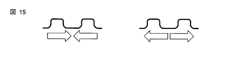
上記のようにして得られた第1及び第2の側壁絶縁膜からなる側壁パターンを、一般的な光学式の合わせずれ検査装置を用いて検査する。図9の側壁により形成される微細パターンの周期は、検査装置の顕微鏡の分解能以下であるため、測定画像は図11のようになる。測定画像には内側の4個の矩形で構成される「インナーマーク」と外側の4個の矩形で構成される「アウターマーク」が存在する。ここで注目すべきは、インナーマークは黒で表示された側壁絶縁膜で外形が規定され、アウターマークは白で表示された側壁絶縁膜で外形が規定されることである。図12は、図11のA−A´線に沿った測定画像のプロファイルである。 The side wall pattern made of the first and second side wall insulating films obtained as described above is inspected using a general optical misalignment inspection apparatus. Since the period of the fine pattern formed by the side wall in FIG. 9 is less than the resolution of the microscope of the inspection apparatus, the measurement image is as shown in FIG. In the measurement image, there are an “inner mark” composed of four inner rectangles and an “outer mark” composed of four outer rectangles. It should be noted that the outer shape of the inner mark is defined by a sidewall insulating film displayed in black, and the outer shape of the outer mark is defined by a sidewall insulating film displayed in white. FIG. 12 is a profile of the measurement image along the line AA ′ in FIG.
図13は、側壁プロセスにおいて1個おきの側壁パターンの寸法(critical dimension:CD)変化があった場合の測定画像の変化を表している。図14は、図13のA−A´線に沿った断面図である。測定画像における各マークのエッジを規定する側壁パターンが、インナーマークとアウターマークで異なるため、1個おきのCDばらつき量の変化とともにインナーマークとアウターマークは、図15に示すように、逆方向に移動することになる。このずれを光学式の合わせずれ検査装置で計測することにより、側壁残しプロセスの不具合に起因する寸法誤差が判明する。 FIG. 13 shows the change in the measurement image when there is a change in the critical dimension (CD) of every other side wall pattern in the side wall process. FIG. 14 is a cross-sectional view taken along line AA ′ of FIG. Since the side wall pattern defining the edge of each mark in the measurement image is different between the inner mark and the outer mark, the inner mark and the outer mark are reversed in the opposite direction as shown in FIG. Will move. By measuring this deviation with an optical misalignment inspection device, a dimensional error due to a defect in the side wall remaining process is found.
上記のように、第1の実施形態においては、側壁残し手法で微細繰り返しパターンを形成する。即ち、側壁残しプロセスを用いて、インナーマークとアウターマークから構成される評価マークを形成し、1本おきのCD変化がインナーマークとアウターマークの相対位置ずれとなるように構成する。この時発生する繰り返しパターンの1本おきのCD変化の発生状況は、一般の光学式合わせずれ検査装置を用いて簡便かつ高速に評価できるので、短時間で結果を半導体装置の製造条件にフィードバックできる。 As described above, in the first embodiment, the fine repeating pattern is formed by the side wall leaving method. That is, an evaluation mark composed of an inner mark and an outer mark is formed using a sidewall leaving process, and every other CD change is a relative positional shift between the inner mark and the outer mark. Since the occurrence of every other CD change of the repeated pattern generated at this time can be evaluated easily and at high speed using a general optical misalignment inspection apparatus, the result can be fed back to the manufacturing conditions of the semiconductor device in a short time. .
(第2の実施形態)
第1の実施形態では、絶縁層パターン3の側壁絶縁膜104を用いて、CD変化を計測したが、絶縁層パターン3の下地層である配線層2の加工パターンを用いて、CD変化を計測しても良い。(Second Embodiment)
In the first embodiment, the CD change is measured using the
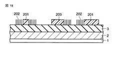
図16は、第2の実施形態に係る計測パターンの形成方法を示す、評価基板の断面図である。即ち、第1の実施形態同様に、半導体基板1上に配線層2を形成し、その上に絶縁層3を形成する。絶縁層3上にレジストパターン4を形成し、これをマスクとして絶縁層3を異方性エッチングする。得られた絶縁層パターン3に側壁絶縁膜104を形成し、その後、絶縁層パターン3を除去する。次いで、側壁絶縁膜104をマスクとして配線層2を異方性エッチングして、配線パターン2からなる評価マークを得る。 FIG. 16 is a cross-sectional view of an evaluation board, illustrating a measurement pattern forming method according to the second embodiment. That is, as in the first embodiment, the
上記において、レジストパターン4を、第1の実施形態の図1のように構成すれば、評価マークとしての配線層パターン2を用いて、第1の実施形態と同様な計測を行なうことができ、同様な効果を奏することができる。 In the above, if the resist
ここで、第2の実施形態で得られる評価マークは、垂直面から成る第1の側面と、湾曲面から成り第1の側面に平行する第2の側面とを有する第1の直線パターンが対を成す第1のマスクと、第1の直線パターンの第2の側面に対向しつつ平行する湾曲面からなる第3の側面と、垂直面からなり前記第3の側面に平行する第4の側面を有する第2の直線パターンが対を成す第2のマスクとを用いて(図16(d))、半導体基板上に形成された下地膜をエッチングすることにより形成された第1及び第2のマーク(図16(e))を具備する。 Here, the evaluation mark obtained in the second embodiment is a pair of first linear patterns having a first side surface composed of a vertical surface and a second side surface composed of a curved surface and parallel to the first side surface. A first mask comprising: a third side surface comprising a curved surface parallel to the second side surface of the first linear pattern; and a fourth side surface comprising a vertical surface and parallel to the third side surface. The first and second layers formed by etching the base film formed on the semiconductor substrate using the second mask in which the second linear pattern having a pair forms a pair (FIG. 16D). A mark (FIG. 16E) is provided.
(第3の実施形態)
第1の実施形態の評価マークでは、64nmL/Sパターンを幅広パターン101、或いは三角パターン103の直交する2側面に1組配置したが、微細なL/Sパターンは多数本設けてもよい。第3の実施形態はこのような例に関する。(Third embodiment)
In the evaluation mark of the first embodiment, a set of 64 nm L / S patterns are arranged on two orthogonal sides of the
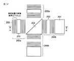
即ち、第3の実施形態では、図17に示すように、図面の左、及び上に配置されたブロック200aでは、幅広パターン201を複数の微細パターン202が、例えば64nmの間隔を開けて挟んで形成されている。図面の右側及び下側のブロック200bにおいては、幅広パターン201と3角パターン203に隣接して複数の微細パターン202が64nmの間隔で形成されている。パターンの長さは、例えば20nmである。図18は、図17のA−A´線に沿った断面図で、第1の実施形態と同一箇所には同一番号を付して重複する説明は省略する。 That is, in the third embodiment, as shown in FIG. 17, in the
上記のようなレジストパターン201〜203を絶縁層3上に形成後、周知の側壁残し法を適用して、図19のように絶縁層3の側面に側壁絶縁膜204を形成する。側壁絶縁膜としては、例えばシリコン窒化膜が使用される。このときの、A−A´線に沿った断面図を図20に示す。 After the resist
さらに絶縁層3を除去し、側壁絶縁膜204を残す。さらに基板全面にレジストを塗布して露光を行い、図21のようにレジストパターン205を形成し、側壁絶縁膜204の露出部分をエッチングにより取り除く。さらにレジストパターン205を剥離すると図22に示された側壁パターン204が基板上に残る。Further, the insulating
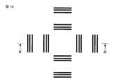
なお、図22は、図21の左右に対向するパターン部のみを取り出した図である。さらに、微細パターン部分には、夫々に側壁パターン204が形成されているが、図19〜22では最外周のもののみ太線で表示している。図22のB−B´線に沿った詳細な断面図を図23に示す。側壁絶縁膜204は、このように形成されている。 Note that FIG. 22 is a diagram in which only the pattern portions facing left and right in FIG. 21 are extracted. Furthermore, although the
上記のようにして得られた側壁絶縁膜204によるパターンを、一般的な光学式の合わせずれ検査装置を用いて検査する。図23に示す側壁絶縁膜204により形成される微細パターンの周期は、検査装置の顕微鏡の分解能以下であるため、測定画像は図11と同様になる。即ち、測定画像には内側の4個の矩形で構成される「インナーマーク」と外側の4個の矩形で構成される「アウターマーク」が存在する。 The pattern by the
図24は、側壁プロセスにおいて1個おきの側壁パターンのCD変化があった場合の測定画像の変化を表している。図25は、図24のB−B´線に沿った断面図である。測定画像における各マークのエッジを規定する側壁パターンが、インナーマークとアウターマークで異なるため、1個おきのCDばらつき量の変化とともにインナーマークとアウターマークは、図24に示すように、逆方向に移動することになる。このずれを光学式の合わせずれ検査装置で計測することにより、側壁残しプロセスの不具合に起因する寸法誤差が判明する。 FIG. 24 shows the change in the measured image when there is a CD change in every other side wall pattern in the side wall process. FIG. 25 is a cross-sectional view taken along the line BB ′ of FIG. Since the side wall pattern that defines the edge of each mark in the measurement image is different between the inner mark and the outer mark, the inner mark and the outer mark are reversed in the opposite direction as shown in FIG. Will move. By measuring this deviation with an optical misalignment inspection device, a dimensional error due to a defect in the side wall remaining process is found.
上記のように、第3の実施形態においては、側壁残し手法で複数の微細繰り返しパターンの一群を形成する。即ち、第1の実施形態と同様に、側壁残しプロセスを用いてインナーマークとアウターマークから構成される評価マークを形成し、1本おきのCD変化がインナーマークとアウターマークの相対位置ずれとなるように構成する。この時発生する繰り返しパターンの1本おきのCD変化の発生状況は、一般の光学式合わせずれ検査装置を用いて簡便かつ高速に評価できるので、短時間で結果を半導体装置の製造条件にフィードバックできる。 As described above, in the third embodiment, a group of a plurality of fine repeating patterns is formed by the side wall leaving method. That is, as in the first embodiment, an evaluation mark composed of an inner mark and an outer mark is formed using a side wall leaving process, and every other CD change becomes a relative positional deviation between the inner mark and the outer mark. Configure as follows. Since the occurrence of every other CD change of the repeated pattern generated at this time can be evaluated easily and at high speed using a general optical misalignment inspection apparatus, the result can be fed back to the manufacturing conditions of the semiconductor device in a short time. .
(第4の実施形態)
第1〜第3の実施形態においては、合わせずれ検査で用いられる、所謂バーインバータイプに類似な評価マークを用いた。本発明はこれに限るものではなく、ボックスインボックスタイプの評価マークを使用することもできる。第4の実施形態では、このような例を説明する。(Fourth embodiment)
In the first to third embodiments, evaluation marks similar to the so-called burn-in bar type used for misalignment inspection are used. The present invention is not limited to this, and a box-in-box type evaluation mark can also be used. In the fourth embodiment, such an example will be described.
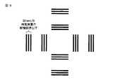
図26は、第4の実施形態で使用される評価パターン(ダミーパターン)の上面図である。中央の小さな正方形には、対角を結んで正方形を2分する三角パターン303が形成されている。小さな正方形を囲んで大きな正方形が形成され、両者に囲まれた環状部分には、複数のL/S微細パターンが夫々環状に平行して形成されている。図中の矢印は、L/Sの長手方向を示す。大きい正方形の右及び上部側辺には、幅広パターン301が形成されている。 FIG. 26 is a top view of an evaluation pattern (dummy pattern) used in the fourth embodiment. In the small square at the center, a
なお、理解を容易にするために、三角パターン303と幅広パターン301にドットを付しているが、実際にドットが存在するわけではなく、領域を明示するために便宜的に付したものである。また、正方形は長方形でもよく、三角パターンは、第1の実施形態同様、必ずしも三角でなくても良い。 In order to facilitate understanding, dots are added to the
上記の評価パターン(ダミーパターン)を用いて、第1の実施形態の図3〜図10と同様な工程を実施する。図27は図26のA−A´線に沿った側壁の断面図で、側壁形成プロセスにおいて1個おきの側壁パターンの寸法変化(CD変化)があった場合の測定画像の変化を表している。即ち、環状パターン部分の、左側と右側では、矢印で示すように、逆方向にパターンの一群が移動することになる。このずれを光学式の合わせずれ検査装置で計測すると、図28に示すような検査画像が得られる。図28(a)は正常な場合、図28(b)はパターンずれが生じた場合である。このようにして、第1の実施形態同様、側壁残しプロセスの不具合に起因する寸法誤差を検出することができる。 Using the above evaluation pattern (dummy pattern), the same processes as those in FIGS. 3 to 10 of the first embodiment are performed. FIG. 27 is a cross-sectional view of the side wall along the line AA ′ in FIG. 26, and shows the change in the measurement image when there is a dimensional change (CD change) of every other side wall pattern in the side wall formation process. . That is, on the left and right sides of the annular pattern portion, a group of patterns moves in the opposite direction as indicated by arrows. When this deviation is measured by an optical misalignment inspection apparatus, an inspection image as shown in FIG. 28 is obtained. FIG. 28A shows a normal case, and FIG. 28B shows a case where a pattern shift occurs. In this manner, as in the first embodiment, it is possible to detect a dimensional error due to a defect in the sidewall leaving process.
上記のように、第4の実施形態においては、側壁残し手法で微細繰り返しパターンの一群をボックスインボックスタイプで形成し、1本おきのCD変化が左側と右側(あるいは、上側と下側)の相対位置ずれとなるように構成する。この時発生する繰り返しパターンの1本おきのCD変化の発生状況は、一般の光学式合わせずれ検査装置を用いて簡便かつ高速に評価できるので、短時間で結果を半導体装置の製造条件にフィードバックできる。 As described above, in the fourth embodiment, a group of fine repetitive patterns is formed in a box-in-box type by the side wall leaving method, and every other CD change is on the left side and the right side (or the upper side and the lower side). The relative position shift is configured. Since the occurrence of every other CD change of the repeated pattern generated at this time can be evaluated easily and at high speed using a general optical misalignment inspection apparatus, the result can be fed back to the manufacturing conditions of the semiconductor device in a short time. .
(第5の実施形態)
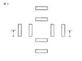
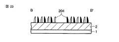
第4の実施形態では、ボックス内の環状部分に、複数の微細パターン302を形成したが、これを幅広パターンとすることもできる。図29は第5の実施形態に係る評価マークの上面図である。第4の実施形態との相異は、ボックス内の環状部分で、三角パターン403に接しない部分を幅広パターン402としていることである。401も幅広パターンである。この評価マークは、第1の実施形態のバーインバータイプの変形例ということもできる。(Fifth embodiment)
In the fourth embodiment, the plurality of
上記の評価パターンを用いて、第1の実施形態の図3〜図10と同様な工程を実施する。図30は図29のA−A´線に沿った側壁の断面図で、側壁形成プロセスにおいて、側壁パターンの寸法変化(CD変化)があった場合の測定画像の変化を表している。本実施形態においては、4本の側壁パターンが観測されるのみであるが、環状パターン部分の左側の2本と右側の2本では、逆方向にパターンが移動することになる。このずれを光学式の合わせずれ検査装置で計測すると、図31に示すような検査画像が得られる。図31(a)は正常な場合、図31(b)はパターンずれが生じた場合である。このようにして、第1の実施形態同様、側壁残しプロセスの不具合に起因する寸法誤差を検出することができる。 Using the above evaluation pattern, the same processes as those in FIGS. 3 to 10 of the first embodiment are performed. FIG. 30 is a cross-sectional view of the side wall along the line AA ′ in FIG. 29, and shows a change in the measurement image when there is a dimensional change (CD change) in the side wall pattern in the side wall forming process. In this embodiment, only four sidewall patterns are observed, but the pattern moves in the opposite direction between the two on the left side and the two on the right side of the annular pattern portion. When this deviation is measured by an optical misalignment inspection apparatus, an inspection image as shown in FIG. 31 is obtained. FIG. 31A shows a normal case, and FIG. 31B shows a case where a pattern shift occurs. In this manner, as in the first embodiment, it is possible to detect a dimensional error due to a defect in the sidewall leaving process.
上記のように、第5の実施形態においても、側壁残し手法で側壁パターンを幅広パターンのみで形成されるバーインバータイプで形成し、CD変化が左側と右側(あるいは、上側と下側)の相対位置ずれとなるように構成する。この時発生する側壁パターンのCD変化の発生状況は、一般の光学式合わせずれ検査装置を用いて簡便かつ高速に評価できるので、短時間で結果を半導体装置の製造条件にフィードバックできる。 As described above, also in the fifth embodiment, the sidewall pattern is formed by the burn-in bar type formed only by the wide pattern by the sidewall leaving method, and the CD change is relative to the left side and the right side (or the upper side and the lower side). It is configured to be misaligned. The occurrence state of the CD change of the side wall pattern generated at this time can be evaluated easily and at high speed using a general optical misalignment inspection apparatus, and the result can be fed back to the manufacturing conditions of the semiconductor device in a short time.
上記の第4及び第5の実施形態においても、図26或いは図29に示すような評価パターン(ダミーパターン)を用いて、その側壁に側壁絶縁膜を形成し、不要部分を除去すると、図27或いは図30に示すような側壁絶縁膜304或いは404からなるマスクが形成される。即ち、側壁絶縁膜(マスク)304或いは404は湾曲面と垂直面とからなる断面形状を有し、ダミーパターンに側壁絶縁膜を形成する工程は、第1の方向に湾曲面がある少なくとも1対の第1の側壁絶縁膜と、第1の方向と逆の第2の方向に湾曲面がある少なくとも1対の第2の側壁絶縁膜を、ダミーパターンの側壁に形成する工程を含み、ダミーパターンを除去する工程は、ダミーパターンを除去して、夫々が一対の第1及び第2の側壁絶縁膜304或いは404を前記第2の下地膜上に残置する工程を含んでいる。 Also in the fourth and fifth embodiments described above, when an evaluation pattern (dummy pattern) as shown in FIG. 26 or FIG. 29 is used to form a side wall insulating film on the side wall and unnecessary portions are removed, FIG. Alternatively, a mask made of the
(第6の実施形態)
第6の実施形態では、第1〜第5の実施形態で説明したパターン評価方法を、半導体装置の製造方法に適用する例について説明する。図32は、第6の実施形態に係る半導体装置製造方法を説明する為のフローチャートである。第1〜第5の実施形態では、ラインアンドスペースの配線パターンを例にとり説明したが、本発明は配線パターンに限定されるものではない。第6の実施形態でも、第1の実施形態の図1〜図10に相当する工程を採用するが、参照番号3の層を下地膜1、参照番号2の層を下地膜2と称することにする。また、半導体製造工程中の随所に挿入される工程であるので、挿入される直前の工程を前工程、直後の工程を次工程とする。(Sixth embodiment)
In the sixth embodiment, an example in which the pattern evaluation methods described in the first to fifth embodiments are applied to a method for manufacturing a semiconductor device will be described. FIG. 32 is a flowchart for explaining a semiconductor device manufacturing method according to the sixth embodiment. In the first to fifth embodiments, the line and space wiring pattern has been described as an example, but the present invention is not limited to the wiring pattern. In the sixth embodiment as well, the steps corresponding to FIGS. 1 to 10 of the first embodiment are adopted. To do. In addition, since the process is inserted everywhere in the semiconductor manufacturing process, the process immediately before the insertion is the previous process, and the process immediately after is the next process.
まず、前工程(S501)より加工中の半導体基板が受け入れ、評価マークによる抜き取り検査を行なう。あるいは先行テストとして実施しても良い。加工中基板に対しレジストを塗布し(S502)、マスクを通じて露光する(S503)。これをベーク・現像し(S504)、レジストのスリミング処理を行なう(S505)。レジストを細らせる必要が特に無い場合は、この工程を省略することができる。 First, a semiconductor substrate being processed is received from the previous step (S501), and a sampling inspection is performed using an evaluation mark. Or you may implement as a prior | preceding test. A resist is applied to the substrate being processed (S502) and exposed through a mask (S503). This is baked and developed (S504), and a resist slimming process is performed (S505). If there is no particular need to make the resist thinner, this step can be omitted.
次に、現像/スリミングにより形成されたレジストパターンを用いて、下地膜1のエッチングを行ない(S506)、側壁を形成する(S507)。この側壁をマスクにして下地膜1を選択的に除去(異方性エッチング)する(S509)。エッチング加工により評価マークが形成された基板は、評価マークに検査に供され(S510)、合格した場合は、次工程に進むことができる(S511)。 Next, the
評価マークの検査(S510)において不合格になった場合、その原因を推定し、エッチング量(時間)の補正が必要な場合は、補正量を算出し下地膜1のエッチング工程(S506)にフィードバックする(S510a)。スリミング量の補正が必要な場合は、補正値が算出されレジストスリミング工程(S505)にフィードバックされる(S510b)。露光量の補正が必要な場合は、補正値が算出され露光工程(S503)にフィードバックされる。 If the evaluation mark inspection (S510) fails, the cause is estimated. If the etching amount (time) needs to be corrected, the correction amount is calculated and fed back to the etching process (S506) of the base film 1 (S510a). If the slimming amount needs to be corrected, a correction value is calculated and fed back to the resist slimming process (S505) (S510b). When exposure amount correction is necessary, a correction value is calculated and fed back to the exposure step (S503).
上記のように、第6の実施形態によれば、評価マークの検査により不具合の状況が短時間で検出できるので、補正値を速やかに半導体装置の製造条件にフィードバックできる。 As described above, according to the sixth embodiment, the status of the defect can be detected in a short time by the inspection of the evaluation mark, so that the correction value can be quickly fed back to the manufacturing conditions of the semiconductor device.
以上、本発明を実施形態を通じ説明したが、本発明は上記実施形態そのままに限定されるものではなく、実施段階ではその要旨を逸脱しない範囲で構成要素を変形して具体化できる。また、上記実施形態に開示されている複数の構成要素の適宜な組み合わせにより、種々の発明を形成できる。例えば、実施形態に示される全構成要素から幾つかの構成要素を削除してもよい。さらに、異なる実施形態にわたる構成要素を適宜組み合わせてもよい。 As mentioned above, although this invention was demonstrated through embodiment, this invention is not limited to the said embodiment as it is, A component can be deform | transformed and embodied in the range which does not deviate from the summary in an implementation stage. In addition, various inventions can be formed by appropriately combining a plurality of constituent elements disclosed in the embodiment. For example, some components may be deleted from all the components shown in the embodiment. Furthermore, constituent elements over different embodiments may be appropriately combined.
1…半導体基板
2…絶縁層(下地層1)
3…配線層(下地層2)
4…レジスト層
5…側壁絶縁層
100a、100b、200a、200b、300a、300b、400a、400b…パターン群
101,201,301、401、402…幅広パターン
102,202,302…微細パターン
103,203,303,403…三角パターン
104,204,304,404…側壁パターンDESCRIPTION OF
3. Wiring layer (underlayer 2)
4 ... Resist
Claims (5)
Translated fromJapanese前記半導体基板にレジストを塗布し、所定のパターンを成すように露光する工程と、
前記露光された半導体基板を現像してレジストマスクを形成する工程と、
前記レジストマスクを用いて、前記第1の下地膜をエッチングしてダミーパターンを形成する工程と、
前記ダミーパターンに側壁絶縁膜を形成する工程と、
前記側壁絶縁膜形成後に、前記ダミーパターンを除去する工程と、
前記側壁絶縁膜を用いて前記第2の下地膜をエッチングして、パターン評価用マークを形成し評価する工程と、
を具備し、
前記ダミーパターンに側壁絶縁膜を形成する工程は、前記側壁絶縁膜は湾曲面と垂直面とからなる断面形状を有し、第1の方向に前記湾曲面がある少なくとも1対の第1の側壁絶縁膜と、前記第1の方向と逆向きの第2の方向に前記湾曲面がある少なくとも1対の第2の側壁絶縁膜を、前記ダミーパターンの側壁に形成する工程を含み、
前記ダミーパターンを除去する工程は、前記ダミーパターンを除去して、夫々が一対の前記第1及び第2の側壁絶縁膜を前記第2の下地膜上に残置する工程を含み、
前記側壁絶縁膜を用いて前記第2の下地膜をエッチングして、パターン評価用マークを形成し評価する工程は、
前記第1の側壁絶縁膜から形成された第1のマスクと、前記第2の側壁絶縁膜から形成された第2のマスクを用いて前記第2の下地膜をエッチングし、前記第2の下地膜に、前記第1のマスクに対応して形成された第1のマークと、前記第2のマスクに対応して形成された第2のマークとを形成するサブ工程と、
前記第1及び第2のマスク、あるいは前記第1及び第2のマークに関して、その相対位置を計測し、夫々の基準位置からのずれを評価するサブ工程と、
を具備することを特徴とするパターン評価方法。Preparing a semiconductor substrate having a first base film formed on an upper surface of the second base film;
Applying a resist to the semiconductor substrate and exposing to form a predetermined pattern;
Developing the exposed semiconductor substrate to form a resist mask;
Etching the first underlayer using the resist mask to form a dummy pattern;
Forming a sidewall insulating film on the dummy pattern;
Removing the dummy pattern after the sidewall insulating film is formed;
Etching the second base film using the sidewall insulating film to form and evaluate a pattern evaluation mark; and
Comprising
In the step of forming a sidewall insulating film on the dummy pattern, the sidewall insulating film has a cross-sectional shape including a curved surface and a vertical surface, and at least a pair of first sidewalls having the curved surface in a first direction. Forming an insulating film and at least one pair of second side wall insulating films having the curved surface in a second direction opposite to the first direction on a side wall of the dummy pattern;
The step of removing the dummy pattern includes a step of removing the dummy pattern and leaving a pair of the first and second sidewall insulating films on the second base film, respectively.
Etching the second base film using the sidewall insulating film to form and evaluate a pattern evaluation mark,
The second base film is etched using the first mask formed from the first sidewall insulating film and the second mask formed from the second sidewall insulating film, and the second underlayer is etched. Forming a first mark corresponding to the first mask and a second mark corresponding to the second mask on the ground film;
A sub-step of measuring the relative positions of the first and second masks or the first and second marks and evaluating deviations from the respective reference positions;
A pattern evaluation method comprising:
前記相対位置を計測するサブ工程において、前記複数の第1若しくは第2の側壁絶縁膜の一群に対応して形成された前記第1及び第2のマスクを夫々一群として認識することを特徴とする請求項1に記載のパターン評価方法。The first and second masks each include a plurality of first or second sidewall insulating films,
In the sub-step of measuring the relative position, the first and second masks formed corresponding to the group of the plurality of first or second sidewall insulating films are respectively recognized as a group. The pattern evaluation method according to claim 1.
前記半導体基板にレジストを塗布し、所定のパターンを成すように露光する工程と、
前記露光された半導体基板を現像してレジストマスクを形成する工程と、
前記レジストマスクに対して、スリミングを実施する選択的な工程と、
前記現像若しくはさらにスリミングされたレジストマスクを用いて、前記第1の下地膜をエッチングしてダミーパターンを形成する工程と、
前記ダミーパターンに側壁膜を形成する工程と、
前記側壁膜形成後に、前記ダミーパターンを除去する工程と、
前記側壁絶縁膜を用いて前記第2の下地膜をエッチングして、パターン評価用マスクを形成する工程と、
前記パターン評価用マスクを用いて、第2の下地膜をエッチングして、前記パターン評価用マスクに対応したパターン評価用マークを形成する工程と、
前記パターン評価用マーク計測して補正の要否を判定し、補正が必要な場合は、前記露光工程、若しくは前記スリミング工程、若しくは前記第1の下地膜のエッチング工程に補正値をフィードバックする工程を具備し、
前記パターン評価用マスクは、
垂直面から成る第1の側面と、湾曲面から成り前記第1の側面に平行する第2の側面とを有する第1の直線パターンが対を成す第1のマスクと、
前記第1の直線パターンの前記第2の側面に対向しつつ平行する湾曲面からなる第3の側面と、垂直面からなり前記第3の側面に平行する第4の側面を有する第2の直線パターンが対を成す第2のマスクと、
を具備することを特徴とする半導体装置の製造方法。Preparing a semiconductor substrate having a first base film formed on an upper surface of the second base film;
Applying a resist to the semiconductor substrate and exposing to form a predetermined pattern;
Developing the exposed semiconductor substrate to form a resist mask;
A selective step of slimming the resist mask;
Etching the first underlayer using the developed or further slimmed resist mask to form a dummy pattern;
Forming a sidewall film on the dummy pattern;
Removing the dummy pattern after forming the sidewall film;
Etching the second base film using the sidewall insulating film to form a pattern evaluation mask;
Etching the second underlayer using the pattern evaluation mask to form a pattern evaluation mark corresponding to the pattern evaluation mask;
The pattern evaluation mark is measured to determine whether correction is necessary, and when correction is necessary, a step of feeding back a correction value to the exposure process, the slimming process, or the etching process of the first base film Equipped,
The pattern evaluation mask is
A first mask that is paired with a first linear pattern having a first side consisting of a vertical plane and a second side consisting of a curved plane and parallel to the first side;
A second straight line having a third side surface formed of a curved surface parallel to the second side surface of the first linear pattern and a fourth side surface formed of a vertical surface and parallel to the third side surface. A second mask pattern pair;
A method for manufacturing a semiconductor device, comprising:
Priority Applications (2)
| Application Number | Priority Date | Filing Date | Title |
|---|---|---|---|
| JP2007050436AJP2008218516A (en) | 2007-02-28 | 2007-02-28 | Pattern evaluation method, evaluation mark, and semiconductor device manufacturing method using the same |
| US12/037,757US8072601B2 (en) | 2007-02-28 | 2008-02-26 | Pattern monitor mark and monitoring method suitable for micropattern |
Applications Claiming Priority (1)
| Application Number | Priority Date | Filing Date | Title |
|---|---|---|---|
| JP2007050436AJP2008218516A (en) | 2007-02-28 | 2007-02-28 | Pattern evaluation method, evaluation mark, and semiconductor device manufacturing method using the same |
Publications (1)
| Publication Number | Publication Date |
|---|---|
| JP2008218516Atrue JP2008218516A (en) | 2008-09-18 |
Family
ID=39838248
Family Applications (1)
| Application Number | Title | Priority Date | Filing Date |
|---|---|---|---|
| JP2007050436APendingJP2008218516A (en) | 2007-02-28 | 2007-02-28 | Pattern evaluation method, evaluation mark, and semiconductor device manufacturing method using the same |
Country Status (1)
| Country | Link |
|---|---|
| JP (1) | JP2008218516A (en) |
Cited By (3)
| Publication number | Priority date | Publication date | Assignee | Title |
|---|---|---|---|---|
| JP2010060388A (en)* | 2008-09-02 | 2010-03-18 | Tokyo Electron Ltd | Pattern shape inspection method and manufacturing method for semiconductor device |
| JP2013195912A (en)* | 2012-03-22 | 2013-09-30 | Toshiba Corp | Mask and manufacturing method of semiconductor device |
| JP2015532733A (en)* | 2012-09-06 | 2015-11-12 | ケーエルエー−テンカー コーポレイション | Device correlation measurement method (DCM) for OVL with embedded SEM structure overlay target |
Citations (4)
| Publication number | Priority date | Publication date | Assignee | Title |
|---|---|---|---|---|
| JP2002280388A (en)* | 2001-03-15 | 2002-09-27 | Toshiba Corp | Method for manufacturing semiconductor device |
| JP2003282663A (en)* | 2002-03-26 | 2003-10-03 | Toshiba Corp | Monitoring method, exposure method, semiconductor device manufacturing method, etching method, and exposure processing apparatus |
| WO2006101695A1 (en)* | 2005-03-15 | 2006-09-28 | Micron Technology, Inc. | Pitch reduced patterns relative to photolithography features |
| JP2007005367A (en)* | 2005-06-21 | 2007-01-11 | Toshiba Corp | Process control system, process control method, and electronic device manufacturing method |
- 2007
- 2007-02-28JPJP2007050436Apatent/JP2008218516A/enactivePending
Patent Citations (4)
| Publication number | Priority date | Publication date | Assignee | Title |
|---|---|---|---|---|
| JP2002280388A (en)* | 2001-03-15 | 2002-09-27 | Toshiba Corp | Method for manufacturing semiconductor device |
| JP2003282663A (en)* | 2002-03-26 | 2003-10-03 | Toshiba Corp | Monitoring method, exposure method, semiconductor device manufacturing method, etching method, and exposure processing apparatus |
| WO2006101695A1 (en)* | 2005-03-15 | 2006-09-28 | Micron Technology, Inc. | Pitch reduced patterns relative to photolithography features |
| JP2007005367A (en)* | 2005-06-21 | 2007-01-11 | Toshiba Corp | Process control system, process control method, and electronic device manufacturing method |
Cited By (3)
| Publication number | Priority date | Publication date | Assignee | Title |
|---|---|---|---|---|
| JP2010060388A (en)* | 2008-09-02 | 2010-03-18 | Tokyo Electron Ltd | Pattern shape inspection method and manufacturing method for semiconductor device |
| JP2013195912A (en)* | 2012-03-22 | 2013-09-30 | Toshiba Corp | Mask and manufacturing method of semiconductor device |
| JP2015532733A (en)* | 2012-09-06 | 2015-11-12 | ケーエルエー−テンカー コーポレイション | Device correlation measurement method (DCM) for OVL with embedded SEM structure overlay target |
Similar Documents
| Publication | Publication Date | Title |
|---|---|---|
| US8072601B2 (en) | Pattern monitor mark and monitoring method suitable for micropattern | |
| TWI520172B (en) | Target and method for mask-to-wafer cd, pattern placement and overlay measurement and control | |
| US7666559B2 (en) | Structure and method for determining an overlay accuracy | |
| JP4971050B2 (en) | Semiconductor device dimension measuring device | |
| TWI804708B (en) | Misregistration metrology system, method for manufacturing semiconductor device wafers, and target for use in measurement of misregistration | |
| JP4511582B2 (en) | Mask pattern correction method, photomask, and semiconductor device manufacturing method | |
| KR20160145637A (en) | Method for evaluating warp in wafer and method for selecting wafer | |
| KR101107354B1 (en) | Pattern formation method, pattern design method and mask set | |
| JP2014187195A (en) | Pattern overlay deviation measuring method | |
| JP5356089B2 (en) | Etching proximity effect correction model creation method, etching proximity effect correction model, mask pattern correction method, photomask, semiconductor device manufacturing method, and semiconductor device | |
| JP2008218516A (en) | Pattern evaluation method, evaluation mark, and semiconductor device manufacturing method using the same | |
| JP5136745B2 (en) | Mask manufacturing error verification method in multiple exposure technology | |
| JP4961750B2 (en) | Semiconductor device manufacturing method and exposure method | |
| JP4525067B2 (en) | Misalignment detection mark | |
| US20050048654A1 (en) | Method of evaluating reticle pattern overlay registration | |
| TWI743792B (en) | Vernier mark for semiconductor manufacturing process and lithographic process inspection method using the same | |
| JP2007206333A (en) | Mask for measuring flare and method for measuring flare | |
| JP2010113195A (en) | Exposure mask, and method of manufacturing semiconductor device | |
| JP2009076863A (en) | Manufacturing method of semiconductor device | |
| JP4541847B2 (en) | Alignment accuracy detection method | |
| JP2013201173A (en) | Pattern formation method | |
| KR20090079713A (en) | Overlay Key of Semiconductor Device and Formation Method | |
| KR100687398B1 (en) | Overlay Measurement Method for Semiconductor Devices | |
| JPS6232783B2 (en) | ||
| CN103176373B (en) | Alignment mark and its preparation method |
Legal Events
| Date | Code | Title | Description |
|---|---|---|---|
| A621 | Written request for application examination | Free format text:JAPANESE INTERMEDIATE CODE: A621 Effective date:20090318 | |
| A977 | Report on retrieval | Free format text:JAPANESE INTERMEDIATE CODE: A971007 Effective date:20111208 | |
| A131 | Notification of reasons for refusal | Free format text:JAPANESE INTERMEDIATE CODE: A131 Effective date:20111220 | |
| A521 | Written amendment | Free format text:JAPANESE INTERMEDIATE CODE: A523 Effective date:20120201 | |
| RD04 | Notification of resignation of power of attorney | Effective date:20120529 Free format text:JAPANESE INTERMEDIATE CODE: A7424 | |
| A02 | Decision of refusal | Effective date:20120605 Free format text:JAPANESE INTERMEDIATE CODE: A02 |