JP2008203445A - Liquid crystal display device - Google Patents
Liquid crystal display deviceDownload PDFInfo
- Publication number
- JP2008203445A JP2008203445AJP2007038284AJP2007038284AJP2008203445AJP 2008203445 AJP2008203445 AJP 2008203445AJP 2007038284 AJP2007038284 AJP 2007038284AJP 2007038284 AJP2007038284 AJP 2007038284AJP 2008203445 AJP2008203445 AJP 2008203445A
- Authority
- JP
- Japan
- Prior art keywords
- liquid crystal
- fpc
- crystal panel
- display device
- crystal display
- Prior art date
- Legal status (The legal status is an assumption and is not a legal conclusion. Google has not performed a legal analysis and makes no representation as to the accuracy of the status listed.)
- Pending
Links
- 239000004973liquid crystal related substanceSubstances0.000titleclaimsabstractdescription88
- 239000000758substrateSubstances0.000claimsabstractdescription41
- 239000011521glassSubstances0.000claimsabstractdescription35
- 238000005452bendingMethods0.000claimsabstractdescription18
- 239000004020conductorSubstances0.000description9
- 239000012788optical filmSubstances0.000description8
- 230000002093peripheral effectEffects0.000description3
- 238000010586diagramMethods0.000description2
- 230000001629suppressionEffects0.000description2
- 230000005540biological transmissionEffects0.000description1
- 239000010408filmSubstances0.000description1
- 238000004519manufacturing processMethods0.000description1
- 230000008054signal transmissionEffects0.000description1
- 238000002834transmittanceMethods0.000description1
Images


Landscapes
- Liquid Crystal (AREA)
Abstract
Description
Translated fromJapanese本発明は、液晶層を駆動するICドライバが、ガラス基板上に実装されたCOG(Chips on glass)方式の液晶パネルを備える液晶表示装置に関する。 The present invention relates to a liquid crystal display device in which an IC driver for driving a liquid crystal layer includes a COG (Chips on glass) type liquid crystal panel mounted on a glass substrate.
従来より、小型化が要求される機器に組み込まれる液晶表示装置として、COG方式の液晶パネルを備える液晶表示装置が提案されている(例えば、特許文献1参照)。 2. Description of the Related Art Conventionally, a liquid crystal display device including a COG type liquid crystal panel has been proposed as a liquid crystal display device incorporated in a device that is required to be downsized (for example, see Patent Document 1).
COG方式の液晶パネルを備える液晶表示装置では、その液晶パネルの裏側のガラス基板の一部が、表側のガラス基板や、それらを挟む2枚の偏光板に対して延設されており、その延設された部分(延設部)には、液晶層を駆動するためのICドライバが実装されている。また、この延設部には、フレキシブルプリント配線板(以下、「FPC」と略述する)の一端が圧着されている。一方、FPCの他端は、機器本体からの信号が伝送される回路基板に圧着されている。このFPCを介して、延設部上のICドライバと回路基板とが電気的に接続されるようになる。
一般的に、液晶パネルは回路基板上に搭載されるため、一端がガラス基板に圧着され、他端が回路基板に圧着されたFPCは、折り曲げられた状態で機器に組み込まれるようになる。このような状態では、FPC内に折り曲げによる内部応力が発生し、それが折り曲げに対する反発力(復元力)となって現われる。この反発力は、FPCの一端が圧着された延設部を中心とする液晶パネルの一部を浮き上がらせようとするため、その浮き上がりを防止すべく何等かの対策が必要となる。 In general, since a liquid crystal panel is mounted on a circuit board, an FPC whose one end is crimped to a glass substrate and the other end is crimped to the circuit board is incorporated into a device in a bent state. In such a state, internal stress due to bending is generated in the FPC, which appears as a repulsive force (restoring force) against the bending. Since this repulsive force tends to lift a part of the liquid crystal panel centering on the extended portion where one end of the FPC is crimped, some countermeasure is required to prevent the lift.
そこで、従来より、FPCに発生する反発力によって液晶パネル1が浮き上がらないように、フックなどの制圧機構を装置内外に取り付けたり、FPCの熱可塑性を利用してFPCを熱変形させ反発力が生じないようにしたりすることが行われていた。しかしながら、FPCの反発力は、製品によって様々であるため、製品ごとに、制圧機構の保持力や、FPCの熱変形の度合いを変更し、調整する必要がある。また、FPCの強引に折り曲げないように、液晶表示装置が組み込まれる携帯機器等の筐体を大きくするなど、筐体の構造設計の変更が必要となったりする場合もある。 In order to prevent the
すなわち、FPCの反発力による液晶パネル1の一部の浮き上がりの防止するためには、機器の設計変更や、新たな部品の追加や、製造工程の追加などが必要となり、これが、製造コストやリードタイムの増大を招来していた。 That is, in order to prevent part of the
本発明は、上記課題を解決するためになされたもので、液晶パネルの一部の浮き上がりを防止する液晶表示装置を提供することを目的とする。 The present invention has been made to solve the above-described problems, and an object thereof is to provide a liquid crystal display device that prevents a part of a liquid crystal panel from being lifted.
本発明においては、上記課題を解決するために、以下の手段を講じた。
(1)基板と、前記基板上に固定されたバックライトユニットと、前記バックライトユニット上に搭載され、液晶層と、当該液晶層を挟む2枚のガラス基板と、当該2枚のガラス基板をさらに挟む2枚の偏光板とを有する液晶パネルであって、前記2枚のガラス基板のうちの裏側のガラス基板が、前記2枚の偏光板及び表側のガラス基板に対して延設された延設部を有し、当該延設部上であってその表側に、前記液晶層を駆動するドライバICが搭載されたCOG方式の液晶パネルと、前記基板と前記ドライバICとを電気的に接続するフレキシブルプリント配線板と、を備え、前記フレキシブルプリント配線板は折り曲げられ、その屈曲部に、少なくとも1つの貫通穴が設けられている液晶表示装置とした。In the present invention, in order to solve the above problems, the following measures are taken.
(1) A substrate, a backlight unit fixed on the substrate, a liquid crystal layer mounted on the backlight unit, two glass substrates sandwiching the liquid crystal layer, and the two glass substrates Further, a liquid crystal panel having two polarizing plates sandwiched therebetween, wherein a glass substrate on the back side of the two glass substrates is extended with respect to the two polarizing plates and the front glass substrate. A COG-type liquid crystal panel on which the driver IC for driving the liquid crystal layer is mounted on the extended portion and on the front side thereof, and the substrate and the driver IC are electrically connected to each other. And a flexible printed wiring board, wherein the flexible printed wiring board is bent and at least one through hole is provided in the bent portion.
(2)前記貫通穴は、前記フレキシブルプリント配線板における折り曲げの曲率が最大となる部分に形成されていることとした。(2) The through hole is formed in a portion where the bending curvature of the flexible printed wiring board is maximized.
上記液晶表示装置によれば、液晶パネルと、プリントフレキシブル配線板の屈曲部に、少なくとも1つの貫通穴が設けられている。このようにすれば、FPCが折り曲げられている部分の断面積を小さくすることができるので、折り曲げによるFPCの内部応力を小さくすることができるようになる。この結果、FPCに反発力による液晶パネルの一部の浮き上がりが防止される。 According to the liquid crystal display device, at least one through hole is provided in the bent portion of the liquid crystal panel and the printed flexible wiring board. In this way, since the cross-sectional area of the portion where the FPC is bent can be reduced, the internal stress of the FPC caused by bending can be reduced. As a result, part of the liquid crystal panel is prevented from being lifted by the repulsive force of the FPC.
以下、本発明の実施形態について、図面に基づいて詳細に説明する。 Hereinafter, embodiments of the present invention will be described in detail with reference to the drawings.
図1には、従来のCOG方式の液晶パネルを備える液晶表示装置の断面図が示されている。図1に示されるように、液晶表示装置10は、液晶パネル1と、バックライトユニット2と、両面テープ3と、ドライバチップ5と、回路基板6と、FPC7とを備えている。 FIG. 1 is a cross-sectional view of a liquid crystal display device including a conventional COG type liquid crystal panel. As shown in FIG. 1, the liquid
液晶パネル1は、図示しない液晶層と、その液晶層を挟む2枚のガラス基板(11A、11B)とを有している。ガラス基板11Aは、−Z側、すなわち裏側のガラス基板であり、ガラス基板11Bは、+Z側、すなわち表側のガラス基板である。液晶パネル1は、液晶層とガラス基板(11A、11B)を挟む2枚の偏光板(12A、12B)をさらに有している。偏光板12Aは、裏側の偏光板であり、偏光板12Bは、表側の偏光板である。 The
ガラス基板11Aには、画素ごとに画素電極(透明電極)が設けられており、ガラス基板11Bには、画素間で共通の共通電極(透明電極)が設けられている。この画素電極と共通電極との間に印加される電圧によって、液晶パネル1の各画素におけるバックライトユニット2からの光の透過率が決定される。液晶表示装置10では、液晶パネル1の各画素の両電極間の電圧が不図示のコントローラによって後述するドライバチップ5を介して制御される。この結果、液晶パネル1の表側の表示面上に画像が表示されるようになる。 The
液晶パネル1は、COG方式の液晶パネルである。ガラス基板11Aは、ガラス基板11B、偏光板(12A、12B)に対して延設された延設部13を有している。この延設部13は、ガラス基板11Aと、ガラス基板11B等とが重なっていない領域であるともいえる。そして、この延設部13の表面側には、液晶層を駆動するためのドライバICとしてのドライバチップ5が設けられている。 The
バックライトユニット2は、フレーム21と、LEDチップ22と、導光板23と、各種光学フィルム24、25、26とを備えている。フレーム21には、LEDチップ22と、導光板23と、各種光学フィルム24〜26とが搭載される。LEDチップ22は、発光ダイオードを有し、液晶表示装置10の光源として発光ダイオードからの光を、導光板23に射出する。導光板23は、LEDチップ22からの光を、液晶パネル1へと導光する。各種光学フィルム24、25、26は、導光板23の表面や裏面に貼り付けられている。光学フィルム24は、導光板23により導かれた光を、液晶パネル1の方へ反射する反射フィルムであり、光学フィルム25、26は、導光板23により導かれた光を散乱させ、液晶パネル1を照明する光を均一化する光学フィルムである。以上の構成を有するバックライトユニット2は、液晶パネル1の全面をほぼ均一に照明する。 The
両面テープ3は、Z軸方向から見て形状が矩形枠状となっているテープである。両面テープ3は、液晶パネル1とバックライトユニット2との間に挿入され、両者の外周部同士を接着固定する。より具体的には、両面テープ3は、一方の面でバックライトユニット2の光学フィルム26の外周部と接着され、他方の面で液晶パネル1の偏光板12Aの外周部と接着されている。これにより、液晶パネル1と、バックライトユニット2とが、両面テープ3を介して接着固定されるようになる。なお、両面テープ3は、バックライトユニット2からの漏れ光を遮光する遮光テープとしての役割も果たしている。 The double-
回路基板6は、液晶表示装置10が組み込まれる機器の本体から供給される電気的な信号を伝送するための伝送回路などが形成された基板である。バックライトユニット2は、両面テープ27により、回路基板6上に接着固定されている。回路基板6上の回路の一部と、バックライトユニット2のLEDチップ22とは、電気的に接続されており、その回路を介してLEDチップ22内の発光ダイオードを発光させるための電力が供給されている。 The circuit board 6 is a board on which a transmission circuit for transmitting an electrical signal supplied from a main body of a device in which the liquid
また、機器本体からの信号が伝送される回路基板6には、FPC7の一端が圧着されており、ガラス基板11Aの延設部13には、FPC7の他端が圧着されている。このFPC7を介して、延設部13上のドライバチップ5と、回路基板6上の駆動信号の伝送回路が電気的に接続されるようになり、回路基板6上の回路からドライバチップ5に、液晶パネル1の駆動信号が供給されるようになる。 In addition, one end of the FPC 7 is crimped to the circuit board 6 to which a signal from the device main body is transmitted, and the other end of the FPC 7 is crimped to the extending
図1に示されるように、液晶パネル1は、この回路基板6上に搭載されるため、ガラス基板11Aと回路基板6とに両端が圧着されたFPC7は、折り曲げられた状態で設置されるようになる。このような状態では、FPC7内に折り曲げ応力が発生し、それが折り曲げに対する反発力(復元力)となって現れる。この結果、ガラス基板11Aの延設部13は、FPC7の反発力によって+Z方向への力を受けるようになる。そして、この力が強すぎると、延設部13を中心とする液晶パネル1の一部が、剥がれて浮き上がる現象が発生するおそれがある。 As shown in FIG. 1, since the
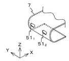
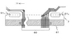
その対策として、FPC7には、2つの貫通穴511、512が設けられている。この貫通穴511、512は、FPC7の折り曲げ部分において最も曲率が大きくなると思われる部分に設けられている。FPC7が折り曲げられると、その折り曲げ部分に内部応力が発生する。この内部応力が大きいと、折り曲げに対する反発力(復元力)となって表れる。この反発力は、FPCの一端が圧着された延設部を中心とする液晶パネルの一部を+Z方向に浮き上がらせようとする。そこで、FPC7では、その折り曲げ部分に2つの貫通穴511、512を設け、最も内部応力が発生しやすい部分の断面積を小さくして、折り曲げに対する内部応力を低減している。As a countermeasure, the FPC7 is provided withtwo through
図2には、本実施形態に係る液晶表示装置10を構成するFPC7の斜視図が示されている。図2に示されるように、FPC7の貫通穴511、512は、横方向(Y軸方向)に長い長穴となっている。この貫通穴511、512の横方向の幅が長くなればなるほど、FPC7の折り曲げによって生ずる反発力が弱くなり、液晶パネル1を浮き上がらせようとする力も弱まるようになる。FIG. 2 is a perspective view of the
図3には、FPC7の内部構造を示す図が示されている。図3では、FPC7を折り曲げずに、延ばした状態が示されている。図3に示されるように、FPC7の中央部には、各種導線パターン群60が配線されており、導線パターン群60が配線されていない両端部に、貫通穴511、512が形成されている。貫通穴511、512の横方向(Y軸方向)の幅は、導線パターン群60を配線するのに必要な幅によって制限される。また、導線パターン群60をFPC7の両端部に配置した場合には、導体パターンの経路長が長くなって抵抗が高くなるため、導体パターン群60は、図3に示されるように、FPC7の中央部に配線されるのが望ましい。これにより、貫通穴511、512は、必然的に、FPC7の側端部に配置されるようになる。FIG. 3 shows a diagram showing the internal structure of the
なお、FPC7の全体の幅を短くしても、FPC7の折り曲げによって生ずる反発力が弱くなるが、この場合には、液晶パネル1のガラス基板11Aとの圧着領域61も小さくなってしまうため、本実施形態のように、FPC7に貫通穴511、512を設け、FPC7の全体の幅については、従来通りのままとするのが望ましい。Even if the overall width of the
なお、FPC7内部の導線パターンの配線の関係上、貫通穴511、512のように、横方向に長い穴を設けることが困難となる場合もある。このような場合には、FPC7の代わりに、図4(A)に示されるようなFPC7’を採用することができる。FPC7’には、貫通穴521、522が設けられている。貫通穴521、522、は、横方向ではなく、縦方向に長い穴となっている。このようにすれば、導体パターン群60の配線領域を確保することができるようになる。Note that it may be difficult to provide a long hole in the lateral direction, such as the through
また、図4(B)に示されるようなFPC7”を採用することができる。図4(B)に示されるように、FPC7”には、貫通穴531、532、533、534が設けられている。貫通穴531、532、533、534は、ミシン目状に配置された小さな貫通穴である。このようなミシン目状に配置された小さな貫通穴は、導線パターン群60の配線密度を粗くしても構わないような場合に、採用することができる。Further, an
なお、これら貫通穴の大きさや間隔は、導線パターン群60の配線に必要な幅などによって制限されることは上述したが、それらについては、FPC7に亀裂が生じて断線したりすることのないように、FPC7自体の強度も考慮して決定されるようにするのが望ましい。 As described above, the size and interval of these through holes are limited by the width necessary for the wiring of the
なお、本実施形態においては、説明を簡略化し、図面の錯綜を防止するために、図1において、液晶表示装置10が備えるドライバチップ5を1つだけ図示したが、実際の液晶表示装置では、ドライバチップ5は複数設けられており、ドライバチップ5ごとにFPC7が設けられる場合もある。このような場合でも、すべてのFPC7において貫通穴511、512を設けるようにするのが望ましい。In the present embodiment, in order to simplify the description and prevent the complication of the drawing, only one driver chip 5 provided in the liquid
以上詳細に説明したように、本実施形態によれば、液晶パネル1と回路基板6とを電気的に接続するFPC1の屈曲部に、少なくとも1つの貫通穴が設けられている。このようにすれば、FPC7の折り曲げによる内部応力を小さくして、その反発力を小さくすることができるようになる。そのため、延設部13を中心とする液晶パネル1の一部の浮き上がりを防止することができる。 As described above in detail, according to the present embodiment, at least one through hole is provided in the bent portion of the
このように、液晶パネル1の一部の浮き上がりを防止すれば、その浮き上がりを防止するための制圧機構を新たに設けたり、FPC7を熱変形させたりする必要がなくなるため、製造コストやリードタイムが増大するのを防ぐことができる。 In this way, if part of the
また、液晶パネル1が浮き上がった状態で、液晶表示装置10を携帯機器などに組み込まないようになるため、組み込み作業の際の液晶パネル1の破損などの発生頻度を低減することができるようになり、歩留まりが向上する。 In addition, since the liquid
また、携帯機器等に組み込まれた後の液晶パネル1の一部の浮き上がりも防止されるようになるので、良好な表示品質をユーザに提供することが可能となる。 In addition, since part of the
また、本実施形態によれば、貫通穴511、512は、FPC7における折り曲げの曲率が最大となる部分に形成されている。折り曲げの曲率が最大となる部分は、FPC7内の折り曲げ応力が最も大きくなる場所であり、このような場所に貫通穴511、512を設ければ、液晶パネル1を浮き上がらせようとする力を、最も効率的に弱めることができるようになる。Further, according to the present embodiment, the through
また、本実施形態では、FPC7の側端部に2つの貫通穴が設けられるようにしたが、いずれか1つの貫通穴はなくてもよい。また、本実施形態では、貫通穴の数を、FPC7の長手方向に1つだけ配置したが、長手方向に複数の貫通穴を配列するようにしてもよい。このように、FPC7に設けられる貫通穴の数は、少なくとも1つ設けられていれば、幾つ設けられていてもよい。 In this embodiment, two through holes are provided in the side end portion of the
また、本実施形態では、貫通穴の形状を、矩形あるいは丸状としたが、本発明は、貫通穴の形状には、制限されない。 In this embodiment, the shape of the through hole is rectangular or round, but the present invention is not limited to the shape of the through hole.
上述したように、本実施形態に係る液晶表示装置10は、FPC7の構造だけが、従来の液晶表示装置と異なるので、携帯機器などに設計変更や負担を強いることなく、液晶表示装置10をその機器に組み込むことができる。 As described above, the liquid
1 液晶パネル
2 バックライトユニット
3 両面テープ
5 ドライバチップ
6 回路基板
7、7’、7” フレキシブルプリント配線板(FPC)
10 液晶表示装置
11A、11B ガラス基板
12A、12B 偏光板
21 フレーム
22 LEDチップ
23 導光板
24、25、26 光学フィルム
27 両面テープ
60 導体パターン群
61 圧着領域DESCRIPTION OF
DESCRIPTION OF
Claims (2)
Translated fromJapanese前記基板上に固定されたバックライトユニットと、
前記バックライトユニット上に搭載され、液晶層と、当該液晶層を挟む2枚のガラス基板と、当該2枚のガラス基板をさらに挟む2枚の偏光板とを有する液晶パネルであって、前記2枚のガラス基板のうちの裏側のガラス基板が、前記2枚の偏光板及び表側のガラス基板に対して延設された延設部を有し、当該延設部上であってその表側に、前記液晶層を駆動するドライバICが搭載されたCOG方式の液晶パネルと、
前記基板と前記ドライバICとを電気的に接続するフレキシブルプリント配線板と、を備え、
前記フレキシブルプリント配線板は折り曲げられ、その屈曲部に、少なくとも1つの貫通穴が設けられている液晶表示装置。A substrate,
A backlight unit fixed on the substrate;
A liquid crystal panel that is mounted on the backlight unit and includes a liquid crystal layer, two glass substrates that sandwich the liquid crystal layer, and two polarizing plates that further sandwich the two glass substrates. Of the two glass substrates, the glass substrate on the back side has an extending portion extended with respect to the two polarizing plates and the front glass substrate, on the extending portion and on the front side, A COG-type liquid crystal panel on which a driver IC for driving the liquid crystal layer is mounted;
A flexible printed wiring board that electrically connects the substrate and the driver IC;
The liquid crystal display device, wherein the flexible printed wiring board is bent and at least one through hole is provided in the bent portion.
前記フレキシブルプリント配線板における折り曲げの曲率が最大となる部分に形成されていることを特徴とする請求項1に記載の液晶表示装置。The through hole is
The liquid crystal display device according to claim 1, wherein the liquid crystal display device is formed in a portion where the bending curvature of the flexible printed wiring board is maximized.
Priority Applications (1)
| Application Number | Priority Date | Filing Date | Title |
|---|---|---|---|
| JP2007038284AJP2008203445A (en) | 2007-02-19 | 2007-02-19 | Liquid crystal display device |
Applications Claiming Priority (1)
| Application Number | Priority Date | Filing Date | Title |
|---|---|---|---|
| JP2007038284AJP2008203445A (en) | 2007-02-19 | 2007-02-19 | Liquid crystal display device |
Publications (1)
| Publication Number | Publication Date |
|---|---|
| JP2008203445Atrue JP2008203445A (en) | 2008-09-04 |
Family
ID=39781036
Family Applications (1)
| Application Number | Title | Priority Date | Filing Date |
|---|---|---|---|
| JP2007038284APendingJP2008203445A (en) | 2007-02-19 | 2007-02-19 | Liquid crystal display device |
Country Status (1)
| Country | Link |
|---|---|
| JP (1) | JP2008203445A (en) |
Cited By (7)
| Publication number | Priority date | Publication date | Assignee | Title |
|---|---|---|---|---|
| WO2012141117A1 (en)* | 2011-04-15 | 2012-10-18 | シャープ株式会社 | Liquid crystal module, and display device |
| CN103048819A (en)* | 2013-01-10 | 2013-04-17 | 友达光电(厦门)有限公司 | Flexible circuit board |
| JP2013134857A (en)* | 2011-12-26 | 2013-07-08 | Koito Mfg Co Ltd | Vehicle lighting fixture |
| US8891035B2 (en) | 2010-02-02 | 2014-11-18 | Nlt Technologies, Ltd. | Display device and FPC board fixing method thereof |
| US9250472B2 (en) | 2013-06-07 | 2016-02-02 | Japan Display Inc. | Liquid crystal display device |
| CN112086493A (en)* | 2020-09-10 | 2020-12-15 | 武汉华星光电半导体显示技术有限公司 | Display device and method of manufacturing the same |
| CN113237414A (en)* | 2021-05-07 | 2021-08-10 | 厦门天马微电子有限公司 | Display module, electronic equipment and alignment precision detection method |
- 2007
- 2007-02-19JPJP2007038284Apatent/JP2008203445A/enactivePending
Cited By (11)
| Publication number | Priority date | Publication date | Assignee | Title |
|---|---|---|---|---|
| US8891035B2 (en) | 2010-02-02 | 2014-11-18 | Nlt Technologies, Ltd. | Display device and FPC board fixing method thereof |
| US9210804B2 (en) | 2010-02-02 | 2015-12-08 | Nlt Technologies, Ltd. | Display device |
| WO2012141117A1 (en)* | 2011-04-15 | 2012-10-18 | シャープ株式会社 | Liquid crystal module, and display device |
| JP2013134857A (en)* | 2011-12-26 | 2013-07-08 | Koito Mfg Co Ltd | Vehicle lighting fixture |
| CN103048819A (en)* | 2013-01-10 | 2013-04-17 | 友达光电(厦门)有限公司 | Flexible circuit board |
| CN103048819B (en)* | 2013-01-10 | 2015-12-23 | 友达光电(厦门)有限公司 | Flexible circuit board |
| TWI617866B (en)* | 2013-01-10 | 2018-03-11 | 友達光電(廈門)有限公司 | Flexible circuit |
| US9250472B2 (en) | 2013-06-07 | 2016-02-02 | Japan Display Inc. | Liquid crystal display device |
| CN112086493A (en)* | 2020-09-10 | 2020-12-15 | 武汉华星光电半导体显示技术有限公司 | Display device and method of manufacturing the same |
| CN113237414A (en)* | 2021-05-07 | 2021-08-10 | 厦门天马微电子有限公司 | Display module, electronic equipment and alignment precision detection method |
| CN113237414B (en)* | 2021-05-07 | 2023-02-28 | 厦门天马微电子有限公司 | Display module, electronic equipment and alignment precision detection method |
Similar Documents
| Publication | Publication Date | Title |
|---|---|---|
| JP4714451B2 (en) | Flexible printed circuit board and liquid crystal display device having the same | |
| US7710528B2 (en) | Electro optical device and electronic apparatus | |
| JP4455570B2 (en) | Flat panel display device and portable display device | |
| CN102088818B (en) | Flexible printed circuit board, backlight unit using the same, and liquid crystal display device comprising the same | |
| JP2008203445A (en) | Liquid crystal display device | |
| JP7094837B2 (en) | Display device, flexible wiring board, and manufacturing method of display device | |
| KR20100077821A (en) | Flexible printed circuit board for led backlight unit and method of fabricating the same | |
| US20100214503A1 (en) | Display panel and repair method thereof | |
| CN103091900B (en) | Liquid crystal indicator | |
| JP5539664B2 (en) | Connector assembly and display device including the same | |
| KR101292569B1 (en) | Liquid crystal display device | |
| KR20090079494A (en) | Liquid crystal display | |
| TWI396892B (en) | Liquid crystal display device | |
| US9123265B2 (en) | Planer light source device with fixing portion and display device using the same | |
| KR102664155B1 (en) | Liquid crystal display device | |
| KR101313649B1 (en) | LCD display device | |
| JP4343200B2 (en) | Portable display device connector | |
| KR20090070944A (en) | Liquid crystal display device | |
| KR20080041994A (en) | Printed circuit board assembly and display device having same | |
| JP2008203728A (en) | Liquid crystal display device | |
| JP2007292826A (en) | Liquid crystal module | |
| JP2009122318A (en) | Display device | |
| JP4312699B2 (en) | Liquid crystal display | |
| WO2019069744A1 (en) | Image display device, method for manufacturing image display device, and component mounting substrate | |
| KR100628435B1 (en) | Assembly method of tiled liquid crystal display and tiled liquid crystal display |