JP2008191649A - Laser light source device, illumination device, image display device, and monitor device - Google Patents
Laser light source device, illumination device, image display device, and monitor deviceDownload PDFInfo
- Publication number
- JP2008191649A JP2008191649AJP2007328968AJP2007328968AJP2008191649AJP 2008191649 AJP2008191649 AJP 2008191649AJP 2007328968 AJP2007328968 AJP 2007328968AJP 2007328968 AJP2007328968 AJP 2007328968AJP 2008191649 AJP2008191649 AJP 2008191649A
- Authority
- JP
- Japan
- Prior art keywords
- light source
- light
- wavelength
- conversion element
- optical path
- Prior art date
- Legal status (The legal status is an assumption and is not a legal conclusion. Google has not performed a legal analysis and makes no representation as to the accuracy of the status listed.)
- Pending
Links
- 238000005286illuminationMethods0.000titleclaimsdescription34
- 230000003287optical effectEffects0.000claimsabstractdescription250
- 238000006243chemical reactionMethods0.000claimsabstractdescription223
- 238000009792diffusion processMethods0.000claimsabstractdescription18
- 238000000034methodMethods0.000claimsdescription27
- 230000008569processEffects0.000claimsdescription25
- 238000003384imaging methodMethods0.000claimsdescription7
- 230000010287polarizationEffects0.000abstractdescription22
- 239000010408filmSubstances0.000description70
- 239000010410layerSubstances0.000description25
- 238000010586diagramMethods0.000description20
- 239000004973liquid crystal related substanceSubstances0.000description18
- 230000004048modificationEffects0.000description15
- 238000012986modificationMethods0.000description15
- 230000003667anti-reflective effectEffects0.000description13
- 238000000926separation methodMethods0.000description12
- 230000009467reductionEffects0.000description11
- 230000000694effectsEffects0.000description10
- 239000000853adhesiveSubstances0.000description9
- 230000001070adhesive effectEffects0.000description9
- 239000002585baseSubstances0.000description8
- 230000005540biological transmissionEffects0.000description7
- 239000000463materialSubstances0.000description7
- 239000004065semiconductorSubstances0.000description7
- 239000000758substrateSubstances0.000description7
- 230000008859changeEffects0.000description5
- 238000013461designMethods0.000description5
- 238000002834transmittanceMethods0.000description5
- 239000013078crystalSubstances0.000description4
- 229910052751metalInorganic materials0.000description4
- 239000002184metalSubstances0.000description4
- 238000005229chemical vapour depositionMethods0.000description3
- 238000009826distributionMethods0.000description3
- 239000011521glassSubstances0.000description3
- 230000000737periodic effectEffects0.000description3
- 239000000470constituentSubstances0.000description2
- 230000001678irradiating effectEffects0.000description2
- 239000005304optical glassSubstances0.000description2
- 239000002356single layerSubstances0.000description2
- YCZZNGRKFVBLDL-UHFFFAOYSA-N2-[(2-methoxyphenyl)methylidene]propanedinitrileChemical compoundCOC1=CC=CC=C1C=C(C#N)C#NYCZZNGRKFVBLDL-UHFFFAOYSA-N0.000description1
- XTTIQGSLJBWVIV-UHFFFAOYSA-N2-methyl-4-nitroanilineChemical compoundCC1=CC([N+]([O-])=O)=CC=C1NXTTIQGSLJBWVIV-UHFFFAOYSA-N0.000description1
- ULPBJGVRVXWECP-UHFFFAOYSA-N3,5-dimethyl-1-(4-nitrophenyl)pyrazoleChemical compoundN1=C(C)C=C(C)N1C1=CC=C([N+]([O-])=O)C=C1ULPBJGVRVXWECP-UHFFFAOYSA-N0.000description1
- XJCVRTZCHMZPBD-UHFFFAOYSA-N3-nitroanilineChemical compoundNC1=CC=CC([N+]([O-])=O)=C1XJCVRTZCHMZPBD-UHFFFAOYSA-N0.000description1
- WSMQKESQZFQMFW-UHFFFAOYSA-N5-methyl-pyrazole-3-carboxylic acidChemical compoundCC1=CC(C(O)=O)=NN1WSMQKESQZFQMFW-UHFFFAOYSA-N0.000description1
- DQFBYFPFKXHELB-UHFFFAOYSA-NChalconeNatural productsC=1C=CC=CC=1C(=O)C=CC1=CC=CC=C1DQFBYFPFKXHELB-UHFFFAOYSA-N0.000description1
- VYZAMTAEIAYCRO-UHFFFAOYSA-NChromiumChemical compound[Cr]VYZAMTAEIAYCRO-UHFFFAOYSA-N0.000description1
- 229910013641LiNbO 3Inorganic materials0.000description1
- 229910003327LiNbO3Inorganic materials0.000description1
- 229910012463LiTaO3Inorganic materials0.000description1
- 229910004298SiO 2Inorganic materials0.000description1
- BQCADISMDOOEFD-UHFFFAOYSA-NSilverChemical compound[Ag]BQCADISMDOOEFD-UHFFFAOYSA-N0.000description1
- 239000003513alkaliSubstances0.000description1
- 230000004075alterationEffects0.000description1
- 229910052782aluminiumInorganic materials0.000description1
- XAGFODPZIPBFFR-UHFFFAOYSA-NaluminiumChemical compound[Al]XAGFODPZIPBFFR-UHFFFAOYSA-N0.000description1
- 230000000903blocking effectEffects0.000description1
- 235000005513chalconesNutrition0.000description1
- 238000004891communicationMethods0.000description1
- 230000003247decreasing effectEffects0.000description1
- 239000006185dispersionSubstances0.000description1
- GQYHUHYESMUTHG-UHFFFAOYSA-Nlithium niobateChemical compound[Li+].[O-][Nb](=O)=OGQYHUHYESMUTHG-UHFFFAOYSA-N0.000description1
- 238000004519manufacturing processMethods0.000description1
- 238000005259measurementMethods0.000description1
- NXIHUWPAXYATMI-UHFFFAOYSA-Nn-(methoxymethyl)-4-nitroanilineChemical compoundCOCNC1=CC=C([N+]([O-])=O)C=C1NXIHUWPAXYATMI-UHFFFAOYSA-N0.000description1
- 239000013307optical fiberSubstances0.000description1
- 230000005693optoelectronicsEffects0.000description1
- 239000011368organic materialSubstances0.000description1
- 229910021420polycrystalline siliconInorganic materials0.000description1
- 229920000642polymerPolymers0.000description1
- 229920005591polysiliconPolymers0.000description1
- 238000002310reflectometryMethods0.000description1
- 229910052709silverInorganic materials0.000description1
- 239000004332silverSubstances0.000description1
- 150000003384small moleculesChemical class0.000description1
- 239000007787solidSubstances0.000description1
- 239000010409thin filmSubstances0.000description1
- DQFBYFPFKXHELB-VAWYXSNFSA-Ntrans-chalconeChemical compoundC=1C=CC=CC=1C(=O)\C=C\C1=CC=CC=C1DQFBYFPFKXHELB-VAWYXSNFSA-N0.000description1
- 239000013585weight reducing agentSubstances0.000description1
Images


Classifications
- H—ELECTRICITY
- H01—ELECTRIC ELEMENTS
- H01S—DEVICES USING THE PROCESS OF LIGHT AMPLIFICATION BY STIMULATED EMISSION OF RADIATION [LASER] TO AMPLIFY OR GENERATE LIGHT; DEVICES USING STIMULATED EMISSION OF ELECTROMAGNETIC RADIATION IN WAVE RANGES OTHER THAN OPTICAL
- H01S5/00—Semiconductor lasers
- H01S5/10—Construction or shape of the optical resonator, e.g. extended or external cavity, coupled cavities, bent-guide, varying width, thickness or composition of the active region
- H01S5/14—External cavity lasers
- H01S5/141—External cavity lasers using a wavelength selective device, e.g. a grating or etalon
- H—ELECTRICITY
- H04—ELECTRIC COMMUNICATION TECHNIQUE
- H04N—PICTORIAL COMMUNICATION, e.g. TELEVISION
- H04N9/00—Details of colour television systems
- H04N9/12—Picture reproducers
- H04N9/31—Projection devices for colour picture display, e.g. using electronic spatial light modulators [ESLM]
- H04N9/3102—Projection devices for colour picture display, e.g. using electronic spatial light modulators [ESLM] using two-dimensional electronic spatial light modulators
- H04N9/3105—Projection devices for colour picture display, e.g. using electronic spatial light modulators [ESLM] using two-dimensional electronic spatial light modulators for displaying all colours simultaneously, e.g. by using two or more electronic spatial light modulators
- H—ELECTRICITY
- H04—ELECTRIC COMMUNICATION TECHNIQUE
- H04N—PICTORIAL COMMUNICATION, e.g. TELEVISION
- H04N9/00—Details of colour television systems
- H04N9/12—Picture reproducers
- H04N9/31—Projection devices for colour picture display, e.g. using electronic spatial light modulators [ESLM]
- H04N9/3141—Constructional details thereof
- H04N9/315—Modulator illumination systems
- H04N9/3161—Modulator illumination systems using laser light sources
- H—ELECTRICITY
- H04—ELECTRIC COMMUNICATION TECHNIQUE
- H04N—PICTORIAL COMMUNICATION, e.g. TELEVISION
- H04N9/00—Details of colour television systems
- H04N9/12—Picture reproducers
- H04N9/31—Projection devices for colour picture display, e.g. using electronic spatial light modulators [ESLM]
- H04N9/3141—Constructional details thereof
- H04N9/315—Modulator illumination systems
- H04N9/3164—Modulator illumination systems using multiple light sources
- G—PHYSICS
- G02—OPTICS
- G02F—OPTICAL DEVICES OR ARRANGEMENTS FOR THE CONTROL OF LIGHT BY MODIFICATION OF THE OPTICAL PROPERTIES OF THE MEDIA OF THE ELEMENTS INVOLVED THEREIN; NON-LINEAR OPTICS; FREQUENCY-CHANGING OF LIGHT; OPTICAL LOGIC ELEMENTS; OPTICAL ANALOGUE/DIGITAL CONVERTERS
- G02F1/00—Devices or arrangements for the control of the intensity, colour, phase, polarisation or direction of light arriving from an independent light source, e.g. switching, gating or modulating; Non-linear optics
- G02F1/01—Devices or arrangements for the control of the intensity, colour, phase, polarisation or direction of light arriving from an independent light source, e.g. switching, gating or modulating; Non-linear optics for the control of the intensity, phase, polarisation or colour
- G02F1/13—Devices or arrangements for the control of the intensity, colour, phase, polarisation or direction of light arriving from an independent light source, e.g. switching, gating or modulating; Non-linear optics for the control of the intensity, phase, polarisation or colour based on liquid crystals, e.g. single liquid crystal display cells
- G02F1/133—Constructional arrangements; Operation of liquid crystal cells; Circuit arrangements
- G02F1/1333—Constructional arrangements; Manufacturing methods
- G02F1/1335—Structural association of cells with optical devices, e.g. polarisers or reflectors
- G02F1/1336—Illuminating devices
- G02F1/133602—Direct backlight
- H—ELECTRICITY
- H01—ELECTRIC ELEMENTS
- H01S—DEVICES USING THE PROCESS OF LIGHT AMPLIFICATION BY STIMULATED EMISSION OF RADIATION [LASER] TO AMPLIFY OR GENERATE LIGHT; DEVICES USING STIMULATED EMISSION OF ELECTROMAGNETIC RADIATION IN WAVE RANGES OTHER THAN OPTICAL
- H01S3/00—Lasers, i.e. devices using stimulated emission of electromagnetic radiation in the infrared, visible or ultraviolet wave range
- H01S3/10—Controlling the intensity, frequency, phase, polarisation or direction of the emitted radiation, e.g. switching, gating, modulating or demodulating
- H01S3/106—Controlling the intensity, frequency, phase, polarisation or direction of the emitted radiation, e.g. switching, gating, modulating or demodulating by controlling devices placed within the cavity
- H01S3/108—Controlling the intensity, frequency, phase, polarisation or direction of the emitted radiation, e.g. switching, gating, modulating or demodulating by controlling devices placed within the cavity using non-linear optical devices, e.g. exhibiting Brillouin or Raman scattering
- H01S3/109—Frequency multiplication, e.g. harmonic generation
- H—ELECTRICITY
- H01—ELECTRIC ELEMENTS
- H01S—DEVICES USING THE PROCESS OF LIGHT AMPLIFICATION BY STIMULATED EMISSION OF RADIATION [LASER] TO AMPLIFY OR GENERATE LIGHT; DEVICES USING STIMULATED EMISSION OF ELECTROMAGNETIC RADIATION IN WAVE RANGES OTHER THAN OPTICAL
- H01S5/00—Semiconductor lasers
- H01S5/005—Optical components external to the laser cavity, specially adapted therefor, e.g. for homogenisation or merging of the beams or for manipulating laser pulses, e.g. pulse shaping
- H01S5/0071—Optical components external to the laser cavity, specially adapted therefor, e.g. for homogenisation or merging of the beams or for manipulating laser pulses, e.g. pulse shaping for beam steering, e.g. using a mirror outside the cavity to change the beam direction
- H—ELECTRICITY
- H01—ELECTRIC ELEMENTS
- H01S—DEVICES USING THE PROCESS OF LIGHT AMPLIFICATION BY STIMULATED EMISSION OF RADIATION [LASER] TO AMPLIFY OR GENERATE LIGHT; DEVICES USING STIMULATED EMISSION OF ELECTROMAGNETIC RADIATION IN WAVE RANGES OTHER THAN OPTICAL
- H01S5/00—Semiconductor lasers
- H01S5/02—Structural details or components not essential to laser action
- H01S5/022—Mountings; Housings
- H01S5/023—Mount members, e.g. sub-mount members
- H01S5/02325—Mechanically integrated components on mount members or optical micro-benches
Landscapes
- Engineering & Computer Science (AREA)
- Multimedia (AREA)
- Signal Processing (AREA)
- Physics & Mathematics (AREA)
- Optics & Photonics (AREA)
- Condensed Matter Physics & Semiconductors (AREA)
- General Physics & Mathematics (AREA)
- Electromagnetism (AREA)
- Optical Modulation, Optical Deflection, Nonlinear Optics, Optical Demodulation, Optical Logic Elements (AREA)
- Semiconductor Lasers (AREA)
- Projection Apparatus (AREA)
- Lasers (AREA)
Abstract
Translated fromJapaneseDescription
Translated fromJapanese本発明は、レーザ光源装置、照明装置、画像表示装置、及びモニタ装置に関する。 The present invention relates to a laser light source device, an illumination device, an image display device, and a monitor device.
近年、光通信、光応用測定、光表示などのオプトエレクトロニクス分野において、レーザ光源装置が広く使用されている。こうしたレーザ光源装置としては、基本波レーザの波長をそのまま利用するものと、基本波レーザの波長を変換して利用するものとがある。後者のレーザ光源装置において、基本波レーザの波長の変換を行う素子として、波長変換素子が知られている。この波長変換素子は、第二次高調波光発生(SHG: Second Harmonic Generation)素子とも呼ばれる。 In recent years, laser light source devices are widely used in the field of optoelectronics such as optical communication, applied optical measurement, and optical display. Such laser light source devices include those that use the wavelength of the fundamental laser as it is, and those that use the wavelength of the fundamental laser after conversion. In the latter laser light source device, a wavelength conversion element is known as an element for converting the wavelength of the fundamental laser. This wavelength conversion element is also referred to as a second harmonic generation (SHG) element.
一般に、SHGの変換効率は30〜40%程度であるため、SHG素子によって変換された光のパワーは、基本波レーザ光源の出力光のパワーに比べてかなり小さくなってしまう。そこで、出力光のパワー低下を抑える構成として、特許文献1のようなレーザ光源装置が提案されている。このレーザ光源装置では、内部共振タイプのレーザ光源から射出され、SHG素子を通過した光を、波長が変換された第一のSHG光と、残余基本波光とに分離する。そして、残余基本波光を、再度SHG素子に通すことによって、波長が変換された第二のSHG光を取り出す。第二のSHG光は、第一のSHG光と偏光方向が90°異なる偏光に変換された状態で、第一のSHG光と合成される。特許文献1のレーザ光源装置では、このようにして、第一のSHG光と第二のSHG光の合成光を出力光として利用することにより、出力光のパワー低下を抑えている。
上記特許文献1に記載のレーザ光源装置では、残余基本波光を、再度SHG素子に通すことによって波長が変換された第二のSHG光を利用することはできるものの、再度SHG素子を通過しても波長が変換されなかった残余基本波光を利用することができない。よって、光の利用効率が劇的に向上することは無い。また、このような残余基本波光を、そのまま基本波レーザ光源へ戻すと、基本波レーザ光源のパワーが低下したり、不安定になってしまったりする恐れがあるため、残余基本波光を光源へ戻さないようにする構成が必須となる。よって、光学系が大型化してしまう可能性がある。また、光路の長さが大きくなったり、光学要素を通過する回数が増えてしまったりするため、光の損失が発生してしまう可能性もある。 In the laser light source device described in Patent Document 1, although the second SHG light whose wavelength is converted by passing the remaining fundamental wave light again through the SHG element can be used, even if it passes through the SHG element again. The residual fundamental wave light whose wavelength has not been converted cannot be used. Therefore, the light utilization efficiency does not improve dramatically. In addition, if such residual fundamental light is returned to the fundamental laser light source as it is, the power of the fundamental laser light source may decrease or become unstable, so the residual fundamental light is returned to the light source. It is essential to have a configuration that does not. Therefore, there is a possibility that the optical system becomes large. Moreover, since the length of the optical path increases or the number of times of passing through the optical element increases, there is a possibility that light loss may occur.
また、特許文献1に記載のレーザ光源装置では、第一のSHG光と第二のSHG光とを合成するために、偏光方向を互いに90°異なる状態にしているため、出力光が2種類の偏光の合成光となってしまう。よって、特許文献1に記載のレーザ光源装置を、1種類の偏光しか利用できない偏光制御型のデバイス(例えば液晶デバイス)と組み合わせて使用することを考えた場合、第一のSHG光と第二のSHG光の偏光方向を揃えるための構成を設けなければ、一方のSHG光しか利用することができなくなってしまう。 Further, in the laser light source device described in Patent Document 1, in order to synthesize the first SHG light and the second SHG light, the polarization directions are different from each other by 90 °, so that there are two types of output light. It becomes the combined light of polarized light. Therefore, when considering using the laser light source device described in Patent Document 1 in combination with a polarization control type device (for example, a liquid crystal device) that can use only one type of polarized light, the first SHG light and the second Unless a configuration for aligning the polarization direction of the SHG light is provided, only one SHG light can be used.
つまり、特許文献1に記載のレーザ光源装置では、出力光のパワー低下をある程度抑え
つつ、安定した出力を得ることは可能であるが、光の利用効率はそれ程上がらない。特に、偏光制御型のデバイスと組み合わせて使用する場合は、光の利用効率が不十分となるおそれもある。
さらに、上記レーザ光源装置と液晶デバイスとを組み合わせる場合には、レーザ光源装置の光を拡散させるための拡散光学部材が必要となる。また、大型の拡散光学部材を介して液晶デバイスに射出された光は、その結像性が低下することから、前記拡散光学部材を小型にすることが望まれている。That is, in the laser light source device described in Patent Document 1, it is possible to obtain a stable output while suppressing a decrease in the power of the output light to some extent, but the light utilization efficiency does not increase so much. In particular, when used in combination with a polarization control type device, the utilization efficiency of light may be insufficient.
Furthermore, when combining the laser light source device and the liquid crystal device, a diffusion optical member for diffusing the light of the laser light source device is required. Further, the light emitted to the liquid crystal device through the large diffusing optical member has a poor image forming property, and therefore it is desired to make the diffusing optical member small.
本発明はこのような事情に鑑みてなされたものであって、出力光のパワー低下が効率よく抑えられ、光利用効率が高く、出力光の偏光方向が揃うことで安定した出力が得られ、かつ拡散光学部材の小型化を可能にした、レーザ光源装置、照明装置、画像表示装置、及びモニタ装置を提供することを目的としている。 The present invention has been made in view of such circumstances, the power reduction of the output light is efficiently suppressed, the light utilization efficiency is high, and a stable output is obtained by aligning the polarization direction of the output light, It is another object of the present invention to provide a laser light source device, an illuminating device, an image display device, and a monitor device that can reduce the size of a diffusing optical member.
本発明のレーザ光源装置は、第一の波長の光を射出する光源と、前記第一の波長の光を選択的に反射して前記光源の方に向かわせる外部共振器と、前記光源と前記外部共振器との間に形成された第一光路上に設けられ、入射した前記第一の波長の光のうち一部の光の波長を前記第一の波長とは異なる第二の波長に変換する波長変換素子と、前記外部共振器によって反射されて前記光源に向かう過程で前記第二の波長に変換された光を、前記第一光路とは異なる第二光路に分離する光路変換素子と、を備え、前記外部共振器から射出される前記第二の波長の第一のレーザ光と、前記光路変換素子から射出される前記第二の波長の第二のレーザ光と、を出力光として利用するレーザ光源装置であって、前記波長変換素子の、該波長変換素子内を透過する光の光軸に直交する線と平行な方向の幅をW1とし、前記波長変換素子の前記外部共振器側の端面における、前記第一のレーザ光と前記第二のレーザ光との光軸間距離をW2としたとき、W2<W1であることを特徴とする。 The laser light source device of the present invention includes a light source that emits light of a first wavelength, an external resonator that selectively reflects light of the first wavelength and directs it toward the light source, the light source, and the light source Provided on the first optical path formed between the external resonator and converts the wavelength of a part of the incident light of the first wavelength into a second wavelength different from the first wavelength. A wavelength converting element, and an optical path converting element that separates the light reflected by the external resonator and converted into the second wavelength in the process toward the light source into a second optical path different from the first optical path; The first laser light having the second wavelength emitted from the external resonator and the second laser light having the second wavelength emitted from the optical path conversion element are used as output light. A laser light source device for transmitting the wavelength conversion element through the wavelength conversion element. The width in the direction parallel to the line orthogonal to the optical axis of the light to be transmitted is W1, and the optical axes of the first laser light and the second laser light on the end face on the external resonator side of the wavelength conversion element When the distance is W2, W2 <W1.
本発明のレーザ光源装置によれば、光源と外部共振器とによって構成された共振構造(第一光路)中に波長変換素子を設け、外部共振器によって反射されて光源へ向かう過程で波長が変換された第二のレーザ光を、光路変換素子によって第二光路に取り出して利用することにより、出力光のパワー低下を効率よく低減することが可能である。また、光源と外部共振器とによって構成された共振構造の内部に波長変換素子を設けているため、外部共振器によって反射されて前記光源の方へ向かう過程で第二の波長に変換されなかった光を光源に戻さないようにする構成を不要にでき、光学系が大型化することで光路の長さが延びる、あるいは光学要素を通過する回数が増えてしまうといった不具合に起因する光の損失を低減することができる。さらに、第二のレーザ光を、第一のレーザ光の進行方向とほぼ同じ方向へ向けるだけで良いため、偏光方向がほぼ揃った出力光を得ることができ、例えば偏光制御型のデバイスと組み合わせて使用する場合であっても、光の利用効率を向上させることができる。
また、W2<W1の関係を満たしているので、前記第二のレーザ光と前記第一のレーザ光との間隔が狭まり、例えばこれら2つのレーザ光の先に拡散光学部材を設ける場合、この拡散光学部材を小型化できる。よって、小型の拡散光学部材を介して射出される光は、結像性の高いものとなり、光の利用効率が高く、鮮明な照度を得ることができる。さらに、本発明によれば、上記関係(W2<W1)を満たしているので、前記光源、前記外部共振器、前記波長変換素子、及び前記光路変換素子の下部側が、例えば接着剤、メカクランプ等の固定部材によって保持される場合においても、第一及び第二のレーザ光が前記固定部材によって遮られるといったことがなくなり、歩留まりの低下を防止することができる。また、レーザ光線が拡散部材の略同一の場所に入射でき略同一な領域への照明を確保できることから、ロスを低減した高効率照明を実現できる。
したがって、レーザ光源装置に組み合わせて用いられる拡散光学部材の小型化を図ることができ、出力光のパワー低下を効率よく抑えて、光利用効率が高く、出力光の偏光方向が揃っており、かつ、出力が安定したレーザ光源装置となる。According to the laser light source device of the present invention, the wavelength conversion element is provided in the resonance structure (first optical path) constituted by the light source and the external resonator, and the wavelength is converted in the process of being reflected by the external resonator and going to the light source. It is possible to efficiently reduce the power reduction of the output light by taking out the second laser light thus obtained into the second optical path by the optical path conversion element and using it. In addition, since the wavelength conversion element is provided inside the resonance structure constituted by the light source and the external resonator, it was not converted into the second wavelength in the process of being reflected by the external resonator and going toward the light source. A configuration that prevents the light from returning to the light source can be eliminated, and the optical system can be increased in size to increase the length of the optical path or increase the number of times that the light passes through the optical element. Can be reduced. Furthermore, since it is only necessary to direct the second laser light in substantially the same direction as the traveling direction of the first laser light, it is possible to obtain output light having substantially the same polarization direction, for example, combined with a polarization control type device. Even if it is used, the utilization efficiency of light can be improved.
Further, since the relationship of W2 <W1 is satisfied, the distance between the second laser beam and the first laser beam is narrowed. For example, when a diffusion optical member is provided at the tip of these two laser beams, this diffusion is performed. The optical member can be reduced in size. Therefore, the light emitted through the small diffusing optical member has a high image forming property, and the light utilization efficiency is high, and clear illuminance can be obtained. Furthermore, according to the present invention, since the relationship (W2 <W1) is satisfied, the lower side of the light source, the external resonator, the wavelength conversion element, and the optical path conversion element is, for example, an adhesive, a mechanical clamp, or the like. Even when held by the fixing member, the first and second laser beams are not blocked by the fixing member, and the yield can be prevented from decreasing. In addition, since the laser beam can be incident on substantially the same location of the diffusing member, and illumination in substantially the same region can be secured, high-efficiency illumination with reduced loss can be realized.
Therefore, it is possible to reduce the size of the diffusing optical member used in combination with the laser light source device, to efficiently suppress the power reduction of the output light, to have high light utilization efficiency, and to align the polarization direction of the output light, and The laser light source device with stable output is obtained.
また、上記レーザ光源装置においては、前記外部共振器の、該外部共振器を透過する前記第一のレーザ光に直交する線と平行な方向の幅をW3としたとき、W2<W3であるのが好ましい。
この構成によれば、上記関係(W2<W1)に加え、さらにW2<W3の関係を満たしているので、例えば外部共振器の下部側を保持している接着剤や保持部材の影響による、光路中に配置された光学部材の透過率低下を回避することができ、光の利用効率をより向上させることができる。また、外部共振器は、光源に対し、外部共振器の反射面を光線方向の長さと、反射角度のアライメントする必要があり位置あわせを容易にしつつ、所望の角度で固定することが容易となり、かつ第2のレーザ光を遮ることを防止できる。In the laser light source device, when the width of the external resonator in the direction parallel to the line perpendicular to the first laser beam passing through the external resonator is W3, W2 <W3. Is preferred.
According to this configuration, since the relationship of W2 <W3 is satisfied in addition to the above relationship (W2 <W1), the optical path, for example, due to the influence of the adhesive or holding member holding the lower side of the external resonator It is possible to avoid a decrease in transmittance of the optical member disposed therein, and it is possible to further improve the light utilization efficiency. In addition, the external resonator needs to be aligned with the length of the light beam direction and the reflection angle of the reflection surface of the external resonator with respect to the light source. In addition, the second laser beam can be prevented from being blocked.
また、上記レーザ光源装置においては、前記第一のレーザ光と前記第二のレーザ光とは、ほぼ平行であるのが好ましい。
レーザ光源装置は、レンズ、フィルダ、ミラー、回折格子、プリズム、光変調素子など、他の光学デバイスと組み合わせて科用される可能性が高いが、このような光学デバイスの多くは、入射光の角度に依存して特性が変化したり、出力結果が変化する場合がある。また、入射光線角度のばらつきによる、照明領域のばらつきでのマージン確保のための照明ロスが発生する。
そこで、本発明を採用すれば、第一のレーザ光と第二のレーザ光とがほぼ平行であるので、レーザ光源装置の後に配置される光学デバイスの設計や配置が容易となる。したがって、特にレーザ光源装置を、画像表示装置やモニタ装置等に応用した場合に、光学設計の自由度が非常に高まるという効果がある。さらに拡散光学部材の先に得られる照明領域がレーザ光線の入射角度に依存した領域に形成されることから、略同一の領域を照明することが可能となり、所望の範囲を照明する高効率照明が可能となる。In the laser light source device, it is preferable that the first laser beam and the second laser beam are substantially parallel.
Laser light source devices are likely to be used in combination with other optical devices such as lenses, filters, mirrors, diffraction gratings, prisms, and light modulation elements, but many of these optical devices are used for incident light. Depending on the angle, the characteristics may change or the output result may change. In addition, an illumination loss for securing a margin due to variations in illumination areas due to variations in incident light angle occurs.
Therefore, when the present invention is adopted, the first laser beam and the second laser beam are substantially parallel, and therefore, the design and arrangement of the optical device arranged after the laser light source device is facilitated. Therefore, particularly when the laser light source device is applied to an image display device, a monitor device or the like, there is an effect that the degree of freedom in optical design is greatly increased. Furthermore, since the illumination area obtained at the tip of the diffusing optical member is formed in an area depending on the incident angle of the laser beam, it is possible to illuminate substantially the same area, and high-efficiency illumination that illuminates a desired range It becomes possible.
また、上記レーザ光源装置においては、前記光路変換素子の、該光路変換素子から射出される前記第二のレーザ光の光線方向の幅をW4とし、前記光路変換素子の、前記波長変換素子内を透過する光の光軸に直交する線と平行な方向の幅をW5としたとき、W4<W5であるのが好ましい。
この構成によれば、光路変換素子における第二のレーザ光の光線方向の大きさが抑えられ、波長変換素子をできるだけ大きくでき、波長変換素子における波長変換光路長を大きく確保できる。よって、波長変換素子における第二の波長への変換効率を向上させ、光の利用効率をより高めることができる。In the laser light source device, the width of the light path direction of the second laser light emitted from the optical path conversion element is W4, and the inside of the wavelength conversion element of the optical path conversion element is within the wavelength conversion element. When the width in the direction parallel to the line perpendicular to the optical axis of the transmitted light is W5, it is preferable that W4 <W5.
According to this configuration, the size of the second laser beam in the light path direction in the optical path conversion element can be suppressed, the wavelength conversion element can be made as large as possible, and the wavelength conversion optical path length in the wavelength conversion element can be secured large. Therefore, the conversion efficiency to the 2nd wavelength in a wavelength conversion element can be improved, and the utilization efficiency of light can be raised more.
また、本発明のレーザ光源装置は、第一の波長の光を射出する光源と、前記第一の波長の光を選択的に反射して前記光源の方に向かわせる外部共振器と、前記光源と前記外部共振器との間に形成される第一光路上に設けられ、入射される前記第一の波長の光のうち、一部の光の波長を前記第一の波長とは異なる第二の波長に変換して高調波を得る波長変換素子と、前記外部共振器によって反射されて前記光源に向かう過程で前記第二の波長に変換された光を、前記第一光路とは異なる第二光路に分離する光路変換素子と、前記波長変換素子における所定の位置から前記第一のレーザ光が出力されるように調整する光路調整手段と、を備え、前記外部共振器から射出される前記第二の波長を有する第一のレーザ光と、前記光路変換素子から射出される前記第二の波長を有する第二のレーザ光と、を出力光として利用することを特徴とする。 The laser light source device of the present invention includes a light source that emits light having a first wavelength, an external resonator that selectively reflects the light having the first wavelength and directs the light toward the light source, and the light source. Is provided on a first optical path formed between the first resonator and the external resonator, and a part of the incident light of the first wavelength is different from the first wavelength. A wavelength converting element for obtaining a higher harmonic wave by converting the wavelength into a second wavelength, and a second light different from the first optical path, which is reflected by the external resonator and converted into the second wavelength in the process toward the light source An optical path conversion element that separates into an optical path; and an optical path adjustment unit that adjusts the first laser beam to be output from a predetermined position in the wavelength conversion element, and the first laser beam emitted from the external resonator A first laser beam having two wavelengths and emitted from the optical path conversion element Characterized by utilizing a second laser beam having the second wavelength, as output light.
本発明のレーザ光源装置によれば、光源と外部共振器とによって構成された共振構造(第一光路)中に波長変換素子を設け、外部共振器によって反射されて光源へ向かう過程で波長が変換された第二のレーザ光を、光路変換素子によって第二光路に取り出して利用することにより、出力光のパワー低下を効率よく低減することが可能である。また、光源と外部共振器とによって構成された共振構造の内部に波長変換素子を設けているため、外部共振器によって反射されて前記光源の方へ向かう過程で第二の波長に変換されなかった光を光源に戻さないようにする構成を不要にでき、光学系が大型化することで光路の長さが延びる、あるいは光学要素を通過する回数が増えてしまうといった不具合に起因する光の損失を低減することができる。さらに、第二のレーザ光を、第一のレーザ光の進行方向とほぼ同じ方向へ向けるだけで良いため、偏光方向がほぼ揃った出力光を得ることができ、例えば偏光制御型のデバイスと組み合わせて使用する場合であっても、光の利用効率を向上させることができる。
また、光路調整手段により、前記第二のレーザ光と前記第一のレーザ光との間隔を狭めることが可能となり、例えばこれら2つのレーザ光の先に拡散光学部材を設ける場合、この拡散光学部材を小型化できる。よって、小型の拡散光学部材を介して射出される光は、結像性の高いものとなり、光の利用効率が高く、鮮明な照度を得ることができる。
また、光路調整手段により、第一のレーザ光をなす第一の波長の光を前記波長変換素子における所定の位置(例えば波長変換素子における分極反転のピッチが安定した部分)に通すことが可能となるので、信頼性を向上させることができる。
したがって、レーザ光源装置に組み合わせて用いる拡散光学部材の小型化を図ることができ、出力光のパワー低下を効率よく抑えて、光利用効率が高く、出力光の偏光方向が揃っており、かつ、出力が安定したレーザ光源装置となる。According to the laser light source device of the present invention, the wavelength conversion element is provided in the resonance structure (first optical path) constituted by the light source and the external resonator, and the wavelength is converted in the process of being reflected by the external resonator and going to the light source. It is possible to efficiently reduce the power reduction of the output light by taking out the second laser light thus obtained into the second optical path by the optical path conversion element and using it. In addition, since the wavelength conversion element is provided inside the resonance structure constituted by the light source and the external resonator, it was not converted into the second wavelength in the process of being reflected by the external resonator and going toward the light source. A configuration that prevents the light from returning to the light source can be eliminated, and the optical system can be increased in size to increase the length of the optical path or increase the number of times that the light passes through the optical element. Can be reduced. Furthermore, since it is only necessary to direct the second laser light in substantially the same direction as the traveling direction of the first laser light, it is possible to obtain output light having substantially the same polarization direction, for example, combined with a polarization control type device. Even if it is used, the utilization efficiency of light can be improved.
Further, the optical path adjusting means can narrow the interval between the second laser beam and the first laser beam. For example, when a diffusion optical member is provided at the tip of the two laser beams, the diffusion optical member is provided. Can be miniaturized. Therefore, the light emitted through the small diffusing optical member has a high image forming property, the light utilization efficiency is high, and clear illuminance can be obtained.
Further, the optical path adjusting means can pass the first wavelength light constituting the first laser beam to a predetermined position in the wavelength conversion element (for example, a portion where the polarization inversion pitch is stable in the wavelength conversion element). Therefore, reliability can be improved.
Therefore, it is possible to reduce the size of the diffusing optical member used in combination with the laser light source device, efficiently suppress the power reduction of the output light, the light utilization efficiency is high, the polarization direction of the output light is aligned, and A laser light source device with stable output is obtained.
また、上記レーザ光源装置においては、前記光路変換素子は、前記光源からの前記第一の波長の光における光路を変換する基本波変換部と、前記第二の波長の光を選択的に反射すること前記第二光路に分離する分離部と、該分離部で分離された前記第二の波長の光の光路を変換して前記第二のレーザ光とする高調波光路変換部と、を有するのが好ましい。
このような光路変換素子を用いることで、上述したような第一のレーザ光と第二のレーザ光を良好に得ることができる。In the laser light source device, the optical path conversion element selectively reflects the fundamental wave conversion unit that converts the optical path in the light of the first wavelength from the light source and the light of the second wavelength. A separation unit for separating into the second optical path, and a harmonic optical path conversion unit for converting the optical path of the light of the second wavelength separated by the separation unit into the second laser light. Is preferred.
By using such an optical path conversion element, the first laser light and the second laser light as described above can be favorably obtained.
また、上記レーザ光源装置においては、前記光路変換素子が前記光路調整手段を含むことが好ましい。
この構成によれば、光路変換素子の一部から光路調整手段が構成されるので、レーザ光源装置の構成を簡略化することができる。Moreover, in the said laser light source apparatus, it is preferable that the said optical path conversion element contains the said optical path adjustment means.
According to this configuration, since the optical path adjusting means is configured from a part of the optical path conversion element, the configuration of the laser light source device can be simplified.
また、上記レーザ光源装置においては、前記光路調整手段は前記光路変換素子を支持する支持部材から構成されるのが好ましい。
この構成によれば、光路変換素子を所定の位置に保持することが可能となり、上述したように第二のレーザ光を確実に外部に取り出すことができる。In the laser light source device, it is preferable that the optical path adjusting means is composed of a support member that supports the optical path conversion element.
According to this configuration, the optical path conversion element can be held at a predetermined position, and the second laser beam can be reliably extracted outside as described above.
また、上記レーザ光源装置においては、前記波長変換素子における一面が保持されており、前記第一のレーザ光の光路は前記波長変換素子の中央部に対し、保持面と反対面側に位置するのが好ましい。
この構成によれば、第一のレーザ光を波長変換素子内に通過させつつ、第二のレーザ光を波長変換素子の外部に通過させるとともに、第一のレーザ光と第二のレーザ光とを近づけることができる。Further, in the laser light source device, one surface of the wavelength conversion element is held, and the optical path of the first laser light is located on the side opposite to the holding surface with respect to the central portion of the wavelength conversion element. Is preferred.
According to this configuration, while allowing the first laser light to pass through the wavelength conversion element, the second laser light is allowed to pass outside the wavelength conversion element, and the first laser light and the second laser light are passed through. You can get closer.
また、上記レーザ光源装置においては、前記光源は、アレイ化された複数の発光部を備えるのが好ましい。
本発明では、このようにアレイ化された光源を用いたとしても、光路変換素子、波長選択素子、及び外部共振器の光入射出端面の面積をアレイに対応した面積に拡張すれば良い。したがって、上記構成によれば、光源がアレイ化されたとしても、装置の過度な大型化を招くことが無く、簡単な構成で対応することが可能である。よって、光源がアレイ化されたとしても、出力光のパワー低下を効率よく抑えることができ、光利用効率が高く、出力光の偏光方向が揃っており、かつ、出力が安定したレーザ光源装置を得ることが可能となる効果をそのまま保持しつつ、アレイ化による光量の増加を、効果的に出力光のパワーアップに繋げることが可能である。In the laser light source device, the light source preferably includes a plurality of light emitting units arranged in an array.
In the present invention, even if the arrayed light sources are used, the area of the light incident / exit end face of the optical path conversion element, wavelength selection element, and external resonator may be expanded to an area corresponding to the array. Therefore, according to the above configuration, even if the light sources are arranged in an array, the apparatus can be handled with a simple configuration without causing an excessive increase in size of the apparatus. Therefore, even if the light sources are arrayed, it is possible to efficiently suppress a reduction in the power of the output light, a high light use efficiency, a uniform polarization direction of the output light, and a stable output of the laser light source device. While maintaining the effect that can be obtained as it is, an increase in the amount of light due to the array can be effectively linked to a power-up of the output light.
また、上記レーザ光源装置においては、前記波長変換素子は、擬似位相制御型の波長変換素子であるのが好ましい。
この構成によれば、他のタイプの波長変換素子に比べて変換効率の高い擬似位相制御型の波長変換素子を備えているので、本発明の効果がより高まる。In the laser light source device, the wavelength conversion element is preferably a quasi phase control type wavelength conversion element.
According to this configuration, since the quasi phase control type wavelength conversion element having higher conversion efficiency than other types of wavelength conversion elements is provided, the effect of the present invention is further enhanced.
本発明の照明装置は、上記のレーザ光源装置と、該レーザ光源装置から射出されたレーザ光の進行方向に配設された拡散光学部材と、を備えることを特徴とする。 An illumination device of the present invention includes the laser light source device described above and a diffusion optical member disposed in a traveling direction of laser light emitted from the laser light source device.
本発明の照明装置によれば、上述したようなレーザ光源装置を備えているので、前記拡散光学部材の小型化が図られ、小型かつ光の結像性の高い高性能なものとなる。 According to the illuminating device of the present invention, since the laser light source device as described above is provided, the diffusing optical member can be miniaturized, and it is small and has a high performance with high light imaging ability.
また、上記レーザ光源装置においては、前記拡散光学部材は、計算機ホログラムからなるのが好ましい。
この構成によれば、計算機ホログラムが小型なものとなり、光の利用効率をより向上させることができる。In the laser light source device, the diffusion optical member is preferably made of a computer generated hologram.
According to this configuration, the computer generated hologram becomes small, and the light utilization efficiency can be further improved.
本発明の画像表示装置は、上記の照明装置からなる光源と、該光源から射出された光を画像情報に応じて変調する光変調素子と、を備えることを特徴とする。 An image display device according to the present invention includes a light source including the illumination device described above, and a light modulation element that modulates light emitted from the light source according to image information.
本発明の画像表示装置によれば、上述したようなレーザ光源装置を有した照明装置を光源として備えているので、光の利用効率が高いものとなる。 According to the image display device of the present invention, since the illumination device having the laser light source device as described above is provided as a light source, the light utilization efficiency is high.
本発明のモニタ装置は、上記のレーザ光源装置あるいは上記の照明装置のいずれか一方と、該レーザ光源装置により照射された被写体を撮像する撮像手段と、を備えることを特徴とする。 A monitor device according to the present invention includes any one of the laser light source device or the illumination device described above, and an imaging unit that captures an image of a subject irradiated by the laser light source device.
本発明のモニタ装置によれば、上述したようなレーザ光源装置を備えているので、光の利用効率が高いものとなる。 According to the monitor device of the present invention, since the laser light source device as described above is provided, the light utilization efficiency is high.
以下、本発明について図面を参照して説明する。なお、以下の全ての図面においては、図面を見やすくするため、各構成要素の膜厚や寸法の比率などは適宜異ならせてある。 The present invention will be described below with reference to the drawings. In all the drawings below, the film thicknesses and dimensional ratios of the constituent elements are appropriately changed in order to make the drawings easy to see.
(第一実施形態)
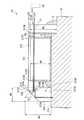
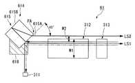
図1は、第一実施形態に係わるレーザ光源装置の概略構成を示す模式図である。レーザ光源装置31は、光源311、波長変換素子(高調波発生素子)312、外部共振器313、光路変換素子314を備えている。光源311は、第一の波長の光を射出する。第一実施形態に係るレーザ光源装置31は、光源311、波長変換素子312、外部共振器313、光路変換素子314が例えば金属フレームなどから構成されたベース部Bに保持されたものとなっている。前記レーザ光源装置31の各構成部材(光源311、波長変換素子312、外部共振器313、光路変換素子314)は、前記ベース部(固定部材)Bに接着剤Cによって固定されている。なお、前記各構成部材を構成する方法としては前記ベース部Bと接着剤との組み合わせに限定されることはなく、例えばメカクランプなどを採用してもよい。(First embodiment)
FIG. 1 is a schematic diagram showing a schematic configuration of the laser light source apparatus according to the first embodiment. The laser
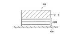
図2は光源311の構造を模式的に示す断面図である。図2に示した光源311は、いわゆる面発光半導体レーザであり、例えば半導体ウエハからなる基板400と、基板400上に形成され、反射ミラーとしての機能を有するミラー層311Aと、ミラー層311Aの表面に積層されるレーザ媒体311Bとを有する。 FIG. 2 is a sectional view schematically showing the structure of the
ミラー層311Aは、基板400上に、例えばCVD(Chemical Vapor Deposition)により形成された、高屈折率の誘電体と低屈折率の誘電体の積層体によって構成されている。ミラー層311Aを構成する各層の厚さ、各層の材料、層の数は、光源311から射出される光の波長(第一の波長)に対して最適化され、反射光が干渉し強め合う条件に設定されている。 The
レーザ媒体311Bは、ミラー層311Aの面上に形成されている。このレーザ媒体311Bは、図示しない電通手段が接続されており、電通手段から所定量の電流が流されると、所定波長の光を射出する。また、レーザ媒体311Bは、ミラー層311Aと、図1に示した外部共振器313との間で、第一の波長の光が共振することにより、特定の波長(第一の波長)の光を増幅させる。すなわち、ミラー層311Aや、後述する外部共振器313により反射された光は、レーザ媒体311Bにより新たに射出される光と共振して増幅され、レーザ媒体311Bの光射出端面からミラー層311Aや基板400に略直交する方向に射出される。 The
波長変換素子312は、入射した光の波長をほぼ半分の波長(第二の波長)の光に変換する。波長変換素子312は、図1に示すように、光源311と外部共振器313との間に形成された第一光路O1上に設けられている。 The
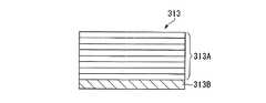
図3は波長変換素子312の構造を模式的に示す断面図である。波長変換素子312は、例えば四角柱形状をなし、波長変換部312Aと、波長変換部312Aの光源311側の面(入射端面)に形成された反射防止(AR:anti-reflective)膜312Bと、波長変換部312Aの外部共振器313側の面(射出端面)に形成されたAR膜312Cとを備えている。 FIG. 3 is a cross-sectional view schematically showing the structure of the
波長変換部312Aは、入射した光の第二高調波を生成する第二次高調波発生(SHG:Second Harmonic Generation)素子である。波長変換部312Aは、周期的な分極反転構造を備えており、擬似位相整合(QPM:Quasi Phase Matching)による波長変換によって、入射した光の波長をほぼ半分の波長(第二の波長)の光に変換する。このようにすれば、他のタイプの波長変換素子に比べて変換効率の高い擬似位相制御型が用いられるので、後述する本発明の効果をより高めている。 The
例えば、光源311から射出される光の波長(第一の波長)が1064nm(近赤外)である場合、波長変換部312Aは、これを半分の波長(第二の波長)532nmに変換して、緑色の光を生成する。ただし、背景技術でも述べたように、波長変換部312Aの波長変換効率は、一般的に30〜 40%程度である。つまり、光源311から射出された光のすべてが、第二の波長の光に変換されるわけではない。 For example, when the wavelength (first wavelength) of light emitted from the
周期的な分極反転構造は、例えばニオブ酸リチウム(LN:LiNbO3)やタンタル酸リチウム(LT:LiTaO3)などの無機非線形光学材料の結晶基板内部に形成されている。具体的には、周期的な分極反転構造は、このような結晶基板内部に、光源311から射出された光に対して略直交する方向に、相互に分極方向が反転した2つの領域312Aa,312Abを、所定の間隔で交互に多数形成した構成となっている。これら2つの領域312Aa,312Abのピッチは、入射光の波長と結晶基板の屈折率分散とを考慮して、適宜決定される。 The periodic domain-inverted structure is formed inside a crystal substrate of an inorganic nonlinear optical material such as lithium niobate (LN: LiNbO3) or lithium tantalate (LT: LiTaO3). Specifically, the periodic domain-inverted structure has two regions 312Aa and 312Ab in which the directions of polarization are inverted in a direction substantially orthogonal to the light emitted from the
なお、一般に半導体レーザから発振されるレーザ光は、利得帯域の中で複数の縦モードが発振し、温度の変動などの影響によりそれらの波長が変化する。すなわち、波長変換素子312において変換される光の波長の許容幅は0.3nm程度であり、使用環境温度の変化に対して、0.1nm/℃程度変動する。 In general, laser light oscillated from a semiconductor laser oscillates in a plurality of longitudinal modes within a gain band, and the wavelengths thereof change due to the influence of temperature fluctuations. That is, the allowable width of the wavelength of light converted by the
AR膜312B,312Cは、例えば単層または多層からなる誘電体膜であり、第一の波長の光および第二の波長の光の双方を例えば98%以上の透過率で透過させる。なお、これらのAR膜312B,312Cは、波長変換素子312の機能を達成する上で必須の構成ではないため、省略することも可能である。つまり、波長変換素子312を、波長変換部312Aのみで構成することも可能である。 The
外部共振器313は、第一の波長の光を選択的に反射して光源311の方に向かわせ、それ以外の波長(第二の波長を含む)の光を透過する機能を有する。外部共振器313は、第一の波長の光を選択的に反射することで、増幅する光の波長を狭帯域化する機能も担っている。外部共振器313は、図1に示すように、第一光路O1上に、第一光路O1に対して略直交するように設けられている。また、その入射端面は、波長変換素子312の射出端面に対向している。 The
図4は外部共振器の構造を模式的に示す断面図である。外部共振器313は、波長変換素子312と同様、四角柱形状をなしている。そして、ブラッグ格子構造が内部に形成された体積型位相格子としてのブラッグ格子部313Aと、その波長変換素子312側の端面(入射端面)に形成された反射防止(AR)膜313Bとを備えている。
ブラッグ格子部313Aは、光路O1に沿って設けられた多数の層によって構成されている。FIG. 4 is a cross-sectional view schematically showing the structure of the external resonator. The
The Bragg
ブラッグ格子部313Aは、SiO2を主体とした例えばアルカリボロアルミノシリケートガラスなどのガラス層に所定波長の紫外線を照射し、ガラス層中に屈折率の異なる干渉パターンを層状に形成したものである。このブラッグ格子部313Aによって、上述した外部共振器313の機能がもたらされる。The Bragg
AR膜313Bは、単層または多層からなる誘電体膜であり、第一の波長の光および第二の波長の光の双方を例えば98%以上の透過率で透過させる。AR膜313Bは、ブラッグ格子部313Aの入射端面だけでなく、射出端面にも形成することが可能である。
なお、AR膜313Bは、外部共振器313の機能を達成する上で必須の構成ではないため、省略することも可能である。つまり、外部共振器313を、ブラッグ格子部313Aのみで構成することも可能である。The
The
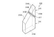
図5は光路変換素子314の斜視図である。光路変換素子314は、図1及び図5に示すように、透光性部材としての第一、及び第二のプリズム315,316と、これらの間に設けられた選択反射膜317とを備えている。 FIG. 5 is a perspective view of the optical
第一のプリズム315は、例えばBK7などの光学ガラスからなり、第一のプリズム315の面315Aは、図1に示すように、光源311と対向するように配置されている。また、この面315Aは、第一光路O1に対して略直交するように配置されている。さらに、面315Bと後述する第二のプリズム316の面316Bとは平行である。また、面315Cは、第一光路O1の光に対して全反射条件を満足する角度に配置された平滑面である。すなわち、第一のプリズム315の面315C及び面315Bは、光源311からの第一の波長の光における光路を変換し、第二のプリズム316に向かわせる基本波変換部として機能する。 The
第二のプリズム316は、第一のプリズム315と同様に、BK7などの光学ガラスからなり、三角柱の形を成している。このプリズム316の側面は、三角形の頂角を挟む二辺を含む面316A,Bと、斜辺を含む面316Cから構成されている。 Similar to the
面316Bには、選択反射膜317が形成されている。この選択反射膜317は、例えば誘電体多層膜によって構成される。このような誘電体多層膜は、例えばCVDによって形成することが可能であり、多層膜を構成する各層の厚さ、各層の材料、層の数は、求められる特性に応じて最適化される。選択反射膜317は、光源311と、波長変換素子312との間に設けられ、第二の波長の光を選択的に反射し、第一の波長の光を透過させる特性を有する。すなわち、前記選択反射膜317は、ダイクロイックミラーとしての機能を備え、これにより面316Bは第二の波長の光を選択的に反射することで上記第一光路O1とは異なる第二光路O2に分離する分離部として機能する。選択反射膜317の、第一波長の光に対する透過率、及び第二波長の光に対する反射率は、高ければ高いほど良いが、80%以上あれば十分である。 A
プリズム315の面315Bは、選択反射膜317が形成されたプリズム316の面316Bと、例えば、紫外線光で硬化する光学用接着剤などにより貼り合わされている。面316Aは、波長変換素子312の一部と対向するように配置されている。また、この面316Aは、第一光路O1に対して略直交するように配置されている。面316Cは、入射光IL(図1参照)に対して全反射条件を満足する角度に配置された平滑面である。面316Cが、入射光ILに対して全反射条件を満足する角度に配置された平滑面とすることで、反射面の反射効率をほぼ100%にすることができ、光の利用効率がより向上したものとなっている。すなわち、上記第二のプリズム316の面316Cは、第二の波長の光を全反射させることができるので、選択反射膜317で分離された第二の波長の光の光路を変換する高調波光路変換部として機能する。なお、高調波光路変換部としては、面316Cに反射膜を設け、この反射膜によって第二のレーザ光LS2を第一のレーザ光LS1の進行方向とほぼ同じ方向へ向けるようにしても良い。このような構成とした場合は、反射効率が多少低下する可能性はあるものの、面316Aを、全反射条件を満足する角度に配置しなくても良いため、光路設計の自由度が増す。 The
プリズム315と316とは貼り合わせによって一体化されている。なお、プリズム315と316とは貼り合わせ以外の方法によって一体化されていても良い。 The
なお、選択反射膜317は、プリズム316の面316Bではなく、プリズム315の面315Bに形成されてもよい。要するに、選択反射膜317は、プリズム315の面315Bと、プリズム316の面316Bの間に設けられていれば良い。また、プリズム315の面315A、プリズム316の面316Aに反射防止(AR)膜を形成してもよい。これらの面にAR膜を形成することにより、これらの面を介して、光路変換素子314に光が入射したり、光路変換素子314から光が射出されたりする際の光の損失を低減することが可能となる。 Note that the
次に、レーザ光源装置31から出力光が得られるまでの過程について説明する。
光源311は、レーザ媒体311Bに電流が流されると、第一の波長の光を射出する。光源311から射出された第一の波長の光は、プリズム315の面315Aから光路変換素子314に入射して、プリズム315の面315Cで全反射された後、プリズム315の面315Bを透過し、選択反射膜317、プリズム316の面316Bをこの順に通過して、プリズム316の面316Aから波長変換素子312に向けて射出される。Next, a process until output light is obtained from the laser
The
光路変換素子314から射出された第一の波長の光は、波長変換素子312に入射する。波長変換素子312では、入射した第一の波長の光のうち一部の光が、半分の波長(第二の波長)に変換される。波長変換素子312から射出された光のうち、第二の波長に変換された光は、外部共振器313を透過して、第一のレーザ光LS1として外部共振器313から射出される。 The light having the first wavelength emitted from the optical
一方、波長変換素子312から射出された光のうち、第二の波長に変換されなかった光(第一波長の光)は、外部共振器313によって反射され、光源311の方に向かう。外部共振器313によって反射された第一の波長の光は、光源311の方へ向かう過程で再び波長変換素子312を通過する。そして、そのうち一部の光が、第二の波長に変換される。 On the other hand, light emitted from the
そして波長変換素子312から光源311の方へ射出された光は、プリズム316の面316Aから光路変換素子314に入射して選択反射膜317に入射する。このようにして選択反射膜317に入射した光のうち、第一の波長の光は、選択反射膜317を透過する。 The light emitted from the
そして、選択反射膜317を透過した第一の波長の光は、プリズム315の面315Bを通過して、プリズム315の面315Cで全反射された後、プリズム315の面315Aから光源311に向けて射出される。
さらに、この光は光源311に戻り、ミラー層311Aによって反射され、再び光源311から射出される。このように、第一の波長の光は、光源311と外部共振器313との間に形成された第一光路O1を往復することにより、レーザ媒体311Bにて新たに発振される光と共振して増幅される。すなわち、レーザ光源装置31は、光源311のミラー層311Aと外部共振器313との間に形成された共振構造を備えている。The first wavelength light transmitted through the
Further, this light returns to the
一方、外部共振器313によって反射されて光源311の方へ向かう過程で波長変換素子312によって第二の波長に変換された光は、選択反射膜317によって反射される。
そして、プリズム316の反射面としての面316Cによって反射されて、第一のレーザ光LS1の進行方向とほぼ平行な方向へ向けられ、第二のレーザ光LS2として、プリズム316の面316Aから射出される。On the other hand, the light reflected by the
Then, the light is reflected by the
すなわち、光路変換素子314は、外部共振器313によって反射されて光源311の方へ向かう過程で第二の波長に変換された光を、第一光路O1とは異なる第二光路O2へ取り出す機能を備えている。そして、光路変換素子314は、このような機能を達成できる限度において、上記第一のプリズム315、第二のプリズム316以外の形状からなるプリズムを用いて構成することも可能である。 That is, the optical
なお、図1において、LS1は、光源311から射出され、波長変換素子312によって第二の波長の光に変換され、第一のレーザ光として外部共振器313から射出される光を示している。光路O1は、光源311から射出された後、波長変換素子312によって第二の波長に変換されること無く、外部共振器313によって反射され光源311に向かう過程においても波長変換素子312にて第二の波長に変換されず、選択反射膜317を透過して光源311に戻る光を示しており、このような光によって光路O1が形成されると考えることができる。さらに、LS2は、光源311から射出され、波長変換素子312によって第二の波長に変換されること無く射出され、外部共振器313によって反射され光源に向かう過程において、波長変換素子312によって第二の波長に変換されて、選択反射膜317へ入射する光を示している。図1では、LS1、O1、LS2を異なる位置に示しているが、これらは説明の便宜上、異なる位置に示されているだけであり、本来は同じ位置に存在する。 In FIG. 1, LS <b> 1 indicates light emitted from the
次に、第一のレーザ光LS1と第二のレーザ光LS2との間の距離と、波長変換素子312の幅および外部共振器313との関係について、図1を参照しながら説明する。図1において、W1は、波長変換素子312の、この波長変換素子312内を透過する光の光軸(第一のレーザ光LS1と第二のレーザ光LS2)に直交する線(図示せず)と平行な方向の幅を示している。W2は、前記波長変換素子312の外部共振器313側の端面における、第一のレーザ光LS1と第二のレーザ光LS2との光軸間距離を示している。 Next, the relationship between the distance between the first laser beam LS1 and the second laser beam LS2, the width of the
ここで、本実施形態に係るレーザ光源装置は、波長変換素子312における所定の位置から第一のレーザ光LS1が出力されるように光源311の光路を調整する光路調整手段を備えている。本実施形態では、光路変換素子314を構成する第一のプリズム315が光路調整手段を含んでいる。すなわち、光路調整手段が光路変換素子314の一部から構成されたものとなっている。第一のプリズム315は、図1に示したように基本波変換部として機能する面315B,315Cを所定の高さに位置させる土台部315D(光路調整手段)を含んでいる。このような構成により、本実施形態に係るレーザ光源装置31は、W2<W1の関係を満たすようになっている。具体的には、W1が0.5mm、W2が0.3mmとなっている。 Here, the laser light source apparatus according to the present embodiment includes an optical path adjusting unit that adjusts the optical path of the
また、上述したように第一のプリズム315(光路変換素子314)及び波長変換素子312はベース部B上に保持されており、第一のレーザ光LS1が波長変換素子312の中央部に対し、保持面(図1中接着剤Cが設けられている面)と反対面側に位置する。この構成により、第一のレーザ光LS1の光路を波長変換素子312内に通過させつつ、第二のレーザ光LS2の光路を波長変換素子312の外部に通過させるとともに、第一のレーザ光LS1と第二のレーザ光LS2とを近づけることができる。 Further, as described above, the first prism 315 (optical path conversion element 314) and the
また、図1においては、W3は、外部共振器313の、この外部共振器313を透過する前記第一のレーザ光LS1に直交する線と平行な方向の幅を示している。本実施形態に係るレーザ光源装置31は、上記関係(W2<W1)に加えて、W2<W3の関係も満たすように構成されている。また、本実施形態では、図1に示したようにW1<W3となっている。具体的には、W3が1.2mmとなっている。 In FIG. 1, W3 indicates the width of the
また、図1においては、W4は、光路変換素子314の、この光路変換素子314から射出される第二のレーザ光LS2の光線方向の幅を示している。W5は、光路変換素子314の、この光路変換素子314内を透過する光(レーザ光LS1)の光軸に直交する線と平行な幅を示している。本実施形態に係るレーザ光源装置31は、W4<W5の関係を満たすように構成されている。具体的には、W4は7mmとなっている。また、W5は、例えば10mm程度となっている。 In FIG. 1, W4 indicates the width of the optical
一般にレーザ光源装置では、光源からの光が焦点を結ぶ位置に外部共振器を配置することで光の利用効率の向上を図っており、外部共振器と光源との間に設けられる波長変換素子の大きさにも制約が生じることとなる。光が波長変換素子を透過する距離が延びる、すなわち波長変換素子における光路長を延ばすことで波長の変換効率を向上させることができる。したがって、レーザ光源装置においては波長変換素子の前記レーザ光LS1,LS2方向の光路長をより長く取るのが望ましい。 In general, in a laser light source device, an external resonator is disposed at a position where light from a light source is focused, thereby improving the light utilization efficiency. A wavelength conversion element provided between the external resonator and the light source is used. There will also be restrictions on the size. The wavelength conversion efficiency can be improved by extending the distance through which light passes through the wavelength conversion element, that is, by extending the optical path length in the wavelength conversion element. Therefore, in the laser light source device, it is desirable to make the optical path length of the wavelength conversion element in the laser light LS1, LS2 direction longer.
一方、本実施形態に係るレーザ光源装置31によれば、前記光路変換素子314が上述した関係(W4<W5)を満たすことで、波長変換素子312の光路長方向における光路変換素子314の大きさが抑えられたものとなっているので、波長変換素子312を出来るだけ大きくでき、これに伴って波長変換素子312における波長変換光路長を長く確保することができる。よって、波長変換素子312における第二の波長への変換効率を向上させ、光の利用効率を高めている。
その他、レーザ光源装置31の具体的な寸法としては、前記波長変換素子312の光路長方向の幅が5mmとなっている。また、光路変換素子314から射出された光の外部共振器313までの光路長(外部共振器313の反射防止313Bの表面と前記光路変換素子314の面316Aとの距離)が8.5mmに設定されている。On the other hand, according to the laser
In addition, as specific dimensions of the laser
本実施形態に係るレーザ光源装置31は、以下の効果を奏する。
(1)光源311と外部共振器313とによって構成された共振構造(第一光路O1)中に波長変換素子312を設け、外部共振器313によって反射されて光源311へ向かう過程で波長が変換された第二のレーザ光を、光路変換素子314によって第二光路O2に取り出して利用することにより、出力光のパワー低下を効率よく低減することが可能である。また、光源311と外部共振器313とによって構成された共振構造の内部に波長変換素子312を設けているため、外部共振器313によって反射されて光源311の方へ向かう過程で第二の波長に変換されなかった光を光源311に戻さないようにする構成が不要となる。よって、光学系の大型化を招く恐れが少なく、光路の長さが長くなったり、光学要素を通過する回数が増えてしまったりすることによる光の損失を低減することもできる。さらに、第二のレーザ光LS2を、第一のレーザ光LS1の進行方向とほぼ同じ方向へ向けるだけで良いため、偏光方向がほぼ揃った出力光を得ることができる。よって、偏光制御型のデバイス(例えば液晶装置)と組み合わせて使用する場合であっても、光の利用効率を向上させることが可能である。The laser
(1) A
(2)上述したように、光路変換素子314が波長変換素子312における所定の位置から第一のレーザ光が出力されるように光源311の光路を調整する光路調整手段を含むので、上述したW2<W1の関係を満たす構成を得ることができる。よって、前記第二のレーザ光LS2と前記第一のレーザ光LS1との間隔を狭めることができる。また、例えばこれら2つのレーザ光LS1,LS2の先に拡散光学部材50を設ける場合、この拡散光学部材50を小型化することができる。よって、このような小型な拡散光学部材50を介して射出される光は、結像性の高いものとなり、後述するような光の利用効率が高く、鮮明な照度が得られる照明装置を提供できる。また、上述したような光路調整手段(土台部315D)を有するので、第一のレーザ光LS1をなす第一の波長の光を波長変換素子312における分極反転のピッチが安定した部分に通すことが可能となり、レーザ光源装置31としての信頼性を向上させることができる。さらに、本発明によれば、前記光源311、前記外部共振器313、前記波長変換素子312、及び前記光路変換素子314の下部側を接着剤Cによってベース部Bに保持した場合でも、この接着剤Cが光路を遮るといった不具合を生じることがなく、この不具合に起因する歩留まりの低下を防止することができる。
したがって、レーザ光源装置に組み合わせて用いられる拡散光学部材50の小型化を図ることができ、出力光のパワー低下を効率よく抑えて、光利用効率が高く、出力光の偏光方向が揃っており、かつ、出力が安定したレーザ光源装置31となる。(2) As described above, the optical
Therefore, it is possible to reduce the size of the diffusing
(3)上記関係(W2<W1)に加え、さらにW2<W3の関係を満たしているので、外部共振器313の下部側を保持している接着剤や保持部材の影響による、光路中に配置された光学部材の透過率低下を回避することができ、光の利用効率をより向上させることができる。また、外部共振器313は、光源に対し、外部共振器313の反射面を光線方向の長さと、反射角度のアライメントする必要があり位置あわせを容易にしつつ、所望の角度で固定することが容易となり、かつ第2のレーザ光LS2を遮ることを防止できる。 (3) In addition to the above relationship (W2 <W1), the relationship of W2 <W3 is satisfied, so that it is arranged in the optical path due to the influence of the adhesive and holding member holding the lower side of the
(4)プリズム315,316の面315A,316Aを介して、光路変換素子314に光を入射させたり、光路変換素子314から光を射出させたりすることができるため、光路変換素子314に入射する光や、光路変換素子314から射出させる光の方向を制御し易い。 (4) Light can enter the optical
(5)一般にレーザ光源装置31は、拡散光学部材、レンズ、フィルタ、ミラー、回折格子、プリズム、光変調素子など、他の光学デバイスと組み合わせて利用される可能性が高いが、このような光学デバイスの多くは、入射光の角度に依存して特性が変化したり、出力結果が変化してしまったりする。また、入射光線角度のばらつきによる、照明領域のばらつきでのマージン確保のための照明ロスが発生する。しかし、本実施形態に係るレーザ光源装置31では、外部共振器313から射出される第一のレーザ光LS1と第二のレーザ光とLS2とがほぼ平行であるため、レーザ光源装置31の後に配置される光学デバイスの設計や配置が容易となる。従って、本実施形態に係るレーザ光源装置31を、画像表示装置やモニタ装置等に応用した場合は、光学設計の自由度が非常に高まるという効果がある。更に拡散光学部材の先に得られる照明領域がレーザ光線の入射角度に依存した領域に形成されることから、略同一の領域を照明することが可能となり、所望の範囲を照明する高効率照明が可能となる。 (5) In general, the laser
(第二実施形態)
図6は、第二実施形態に係わるレーザ光源装置41の概略構成を示す模式図である。第二実施形態のレーザ光源装置41は、光路変換素子414の構成だけが第一実施形態のレーザ光源装置31と異なっており、それ以外は、前記第一実施形態と同様である。したがって、図6において、第一実施形態と同一部材には同一符号を付して、その説明は省略または簡略化する。また、レーザ光源装置41から出力光が得られるまでの過程についても同様であり、その詳細な説明も省略または簡略化する。(Second embodiment)
FIG. 6 is a schematic diagram showing a schematic configuration of a laser
図6に示すレーザ光源装置41において、光路変換素子414は、透光性部材としての板状部材(図示せず)と、選択反射膜317と、反射ミラー416とを備えている。板状部材の第1の面に選択反射膜317が形成され、板状部材の第2の面に反射ミラー416が設けられている。 In the laser
反射ミラー416は、選択反射膜317と同様、誘電体多層膜によって構成することが可能である。このとき、反射ミラー416を構成する誘電体多層膜は、選択反射膜317と異なる誘電体多層膜でも良いが、同じ誘電体多層膜でも良い。また、反射ミラー416はアルミニウム、クロム、銀などの金属膜によって構成しても良い。一般的に、誘電体多層膜の方が、金属膜に比べて耐熱性に優れている。また、誘電体多層膜は、これを構成する各層の厚さ、各層の材料、層の数の最適化により、特定波長の光に対する反射率を高めることが可能であり、レーザ光のように波長帯域が狭く、指向性の高い光を効率よく反射するにも適している。一方、金属膜は、コスト面において誘電体多層膜よりも有利である。 Similar to the
なお、選択反射膜317および反射ミラー416が形成された面とは反対側の面に反射防止(AR)膜を形成するのが好ましい。これらの面にAR膜を形成することにより、これらの面を介して、光路変換素子414に光が入射したり、光路変換素子414から光が射出されたりする際の光の損失を低減することが可能となる。 An antireflection (AR) film is preferably formed on the surface opposite to the surface on which the
次に、レーザ光源装置41から出力光が得られるまでの過程について、図6を参照して説明する。光源311は、第一の波長の光を射出する。光源311から射出された第一の波長の光は、光路変換素子414に入射して、選択反射膜317を通過して、波長変換素子312に向けて射出される。すなわち、本実施形態に係るレーザ光源装置41は、光源311の光射出面が波長変換素子312の反射防止膜312Bにほぼ対向するように配置されている。光路変換素子414から射出された第一の波長の光は、波長変換素子312に入射する。波長変換素子312では、入射した第一の波長の光のうち一部の光の波長が、半分の波長(第二の波長)に変換される。波長変換素子312から射出された光のうち、第二の波長に変換された光は、外部共振器313を透過して、第一のレーザ光LS1として外部共振器313から射出される。 Next, a process until output light is obtained from the laser
一方、波長変換素子312から射出された光のうち、第二の波長に変換されなかった光(第一波長の光)は、外部共振器313によって反射され、光源311の方に向かう。外部共振器313によって反射された第一の波長の光は、光源311の方へ向かう過程で再び波長変換素子312を通過する。そして、そのうち一部の光の波長が、第二の波長に変換される。そして波長変換素子312から光源311の方へ射出された光は、選択反射膜317に入射する。 On the other hand, light emitted from the
このようにして選択反射膜317に入射した光のうち、第一の波長の光は、選択反射膜317を透過する。そして、選択反射膜317を透過した第一の波長の光は、光路変換素子414から光源311に向けて射出される。さらに、この光は光源311に戻り、その内部に設けられたミラー層によって反射され、再び光源311から射出される。このように、第一の波長の光は、光源311と外部共振器313との間に形成された第一光路O1を往復することにより、レーザ媒体311Bにて新たに発振される光と共振して増幅される。すなわち、レーザ光源装置41は、光源311の内部に設けられたミラー層と外部共振器313との間に形成された共振構造を備えている。 Of the light incident on the
一方、外部共振器313によって反射されて光源311の方へ向かう過程で波長変換素子312によって第二の波長に変換された光は、選択反射膜317によって反射される。
そして、反射ミラー416によって反射されて、第一のレーザ光LS1の進行方向とほぼ平行な方向へ向けられ、第二のレーザ光LS2として射出される。On the other hand, the light reflected by the
Then, the light is reflected by the
本実施形態に係るレーザ光源装置41においても、第一実施形態の上記効果(1)、(2)、(4)〜(6)に加え、以下の効果を奏することができる。
透光性部材としてプリズムを用いた場合よりも、軽量な光路変換素子414を得ることができる。また、板状部材はプリズムに比べて加工が容易である。よって、レーザ光源装置の軽量化及び低コスト化に寄与することができる。In the laser
A lighter
(実施形態の変形例)
本発明は前述の第一実施形態及び第二実施形態に限定されるものではなく、本発明の目的を達成できる範囲での変形、改良等は本発明に含まれるものである。以下に変形例として挙げられているような形態であっても、前述の実施形態と同様な効果を得ることができる。(Modification of the embodiment)
The present invention is not limited to the first and second embodiments described above, but includes modifications and improvements as long as the object of the present invention can be achieved. Even if it is a form which is mentioned as a modification below, the same effect as the above-mentioned embodiment can be acquired.
光源311としては、面発光型半導体レーザ以外に、いわゆる端面発光型半導体レーザまたは半導体励起固体レーザを用いることができる。なお、端面発光型半導体レーザを用いる場合には、光源311と光路変換素子314,414との間に、光源311から射出された光を平行化するためのレンズを設けることが好ましい。 As the
また、光源311は、アレイ化された複数の発光部を備えたものとすることができる。図7(a)及び図7(b)は、いずれも発光部がアレイ化された光源を示す模式図である。図7(a)の光源321では、複数の発光部322が一列に並んでいる。また、図7(b)の光源323では、複数の発光部322が2列に並んでいる。なお、発光部の数や、列の数は、図7(a)や(b)に示したものには限らない。上述したレーザ光源装置31,41では、このように発光部がアレイ化された光源を用いたとしても、選択反射膜、反射面、波長選択素子や外部共振器の光入射出端面の面積を、アレイに対応した面積に拡張すれば良いだけである。 Further, the
このように、上述したレーザ光源装置31,41では、光源がアレイ化されたとしても、装置の過度な大型化を招くことが無く、簡単な構成で対応することが可能である。よって、上述したレーザ光源装置31,41では、光源がアレイ化されたとしても、出力光のパワー低下を効率よく抑えて、光利用効率が高く、出力光の偏光方向が揃っており、かつ、出力が安定したレーザ光源装置を得ることが可能となる効果をそのまま保持しつつ、アレイ化による光量の増加を、効果的に出力光のパワーアップに繋げることが可能である。 As described above, in the laser
波長変換素子312を構成する非線形光学材料としては、先にLN(LiNbO3)や、LT(LiTaO3)を例示したが、これ以外にもKNbO3、BNN(Ba2NaNb5O15)、KTP(KTiOPO4)、KTA(KTiOAsO4)、BBO(β―BaB2O4)、LBO(LiB3O7)などの無機非線形光学材料を利用してもよい。また、メタニトロアニリン、2−メチル−4−ニトロアニリン、カルコン、ジシアノビニルアニソール、3,5−ジメチル−1−(4−ニトロフェニル)ピラゾール、N−メトキシメチル−4−ニトロアニリンなどの低分子有機材料や、ポールドポリマなどの有機非線形光学材料を用いてもよい。The nonlinear optical material constituting the
波長変換素子312として、上述したSHG素子に変えて、第三次高調波発生素子を用いても良い。 As the
外部共振器313としては、先に説明した体積型位相格子以外に、結晶型の体積ホログラム、フォトポリマ体積ホログラム、ブレーズド型回折格子(溝の断面形状が鋸歯状である回折格子)などを用いても良い。 As the
また、上記実施形態では外部共振器313が波長選択を行うとともに、可視光を透過する構成となっていたが、図8に示すようにバンドパスフィルタBPとワイドバンドミラーMとの組み合わせることで上記共振器を構成するようにしてもよい。バンドパスフィルタBPとは、ある波長、または波長帯の光を透過させ、その短波長側、および長波長側の光を反射させるフィルタである。また、図8に示されるように、光の入射角度を変化させることにより透過波長が調整され、波長選択が行われる。この場合、バンドパスフィルタBPによって波長選択を行う、ワイドバンドミラーMが可視光を透過するミラーとして機能する。このとき、図1に示した外部共振器の幅W3は、前記ワイドバンドミラーMの幅に対応する。 In the above embodiment, the
(照明装置)
次に、本発明に係る照明装置の一実施形態として、例えば上記レーザ光源装置41を応用した照明装置500の構成例について説明する。図9は、照明装置500の概略を示す模式図である。なお、図9中においては図示を簡略化し、光路変換素子414の図示を省略している。
図9に示すように、照明装置500は、前記レーザ光源装置41と、該レーザ光源装置41から発したレーザ光を拡散するとともに、レーザ光の照度分布を均一化する拡散光学部材50とを備えている。この拡散光学部材50としては、ホログラム素子から構成されている。具体的には、ホログラム原板に計算機で計算して人工的に作成した干渉縞が形成された計算機ホログラム(CGH:Computer Generated Hologram)を用いることがきできる。計算機ホログラムは、回折格子の分割領域の自由な設定が可能であり、収差の問題が生じないので好適である。(Lighting device)
Next, as an embodiment of the illumination device according to the present invention, a configuration example of an
As shown in FIG. 9, the
一般に、計算機ホログラムから構成される拡散光学部材50には、例えば製造誤差等の要因によりムラが生じ、鮮明な光が得られなくなることがある。このような現象は、特に拡散光学部材が大型化した際に顕著となる。また、小型な拡散光学部材は光の結像性が高く、被照射物に鮮明かつ均一な照度分布を有した光照射を行うことが可能である。すなわち、拡散光学部材を小型化することが望まれている。 In general, the diffusing
本実施形態に係る照明装置500によれば、上述したようなレーザ光源装置41を備えているので、前記拡散光学部材14の小型化が図られており、光の結像性が高いものとなる。よって、被照射物に鮮明かつ均一な照度分布を有した光照射を行うことのできる高性能なものとなる。 According to the
(画像表示装置)
次に、第一の実施形態に係るレーザ光源装置31を応用した画像表示装置の一例として、プロジェクタ3の構成について説明する。図10は、プロジェクタ3の光学系の概略を示す模式図である。(Image display device)
Next, a configuration of the
図10において、プロジェクタ3は、光源として上記照明装置500、光変調装置としての液晶パネル(光変調素子)32、偏光板331及び332、クロスダイクロイックプリズム34、投射レンズ35などを備えている。なお、液晶パネル32と、その光入射側に設けられた偏光板331及び光射出側に設けられた偏光板332によって液晶ライトバルブ33が構成される。 10, the
照明装置500は、赤色レーザ光を射出する赤色光用光源装置500Rと、青色レーザ光を射出する青色光用光源装置500Bと、緑色レーザ光を射出する緑色光用光源装置500Gとから構成されたものとなっている。これらの光源装置500(500R,G,B)は、それぞれクロスダイクロイックプリズム34の側面三方にそれぞれ対向するように配置されている。図10では、クロスダイクロイックプリズム34を挟んで、赤色光用光源装置500Rと青色光用光源装置500Bとが互いに対向し、投射レンズ35と緑色光用光源装置500Gが互いに対向しているが、これらの位置は、適宜入れ替えることが可能である。 The
液晶パネル32は、例えば、ポリシリコンTFT(Thin Film Transistor)をスイッチング素子として用いたものである。各照明装置500から射出された色光は、入射側偏光板331を介して液晶パネル32に入射する。液晶パネル32に入射した光は、画像情報に応じて変調されて、液晶パネル32から射出される。液晶パネル32によって変調された光のうち、特定の直線偏光だけが、射出側偏光板332を透過して、クロスダイクロイックプリズム34に向かう。 The
クロスダイクロイックプリズム34は、各液晶パネル32によって変調された各色光を合成して、カラー画像を形成する光学素子である。このクロスダイクロイックプリズム34は、4つの直角プリズムを貼り合わせた平面視略正方形状をなしている。そして、これら4つの直角プリズムの界面には、2種類の誘電体多層膜がX字状に設けられている。これら誘電体多層膜は、互いに対向する各液晶パネル32から射出された各色光を反射し、投射レンズ35に対向する液晶パネル32から射出された色光を透過する。このようにして、各液晶パネル32にて変調された各色光が合成されて、カラー画像が形成される。 The cross
投射レンズ35は、複数のレンズが組み合わされた組レンズとして構成される。この投射レンズ35は、カラー画像Lを拡大投射する。 The
本実施形態に係るプロジェクタ3によれば、上述したようなレーザ光源装置を備えた照明装置が光源として用いられているので、光の利用効率が高いものとなる。 According to the
なお、本実施形態では、上記照明装置500(500R,G,B)を用いているが、これらのうち一部もしくは全部を、他の実施形態に係るレーザ光源装置31あるいは上述した変形例に係るレーザ光源装置に置き換えても良い。 In the present embodiment, the illumination device 500 (500R, G, B) is used. However, some or all of them relate to the laser
この実施形態では、光変調素子を3つ用いたプロジェクタの例について説明したが、光変調装置を1つ、2つ、あるいは4つ以上用いたプロジェクタにも適用することができる。また、この実施形態では、透過型のプロジェクタについて説明したが、上記照明装置500あるいは照明装置を構成するレーザ光源装置31,41は、反射型プロジェクタにも適用することが可能である。ここで、「透過型」とは、光変調素子が光を透過するタイプであることを意味しており、「反射型」とは、光変調素子が光を反射するタイプであることを意味している。 In this embodiment, an example of a projector using three light modulation elements has been described, but the present invention can also be applied to a projector using one, two, or four or more light modulation devices. In this embodiment, the transmissive projector has been described. However, the
また、光変調素子は液晶パネル32に限られず、例えばマイクロミラーを用いたデバイスであっても良い。さらに、プロジェクタとしては、投射面を観察する方向から画像投射を行うフロントタイプと、投射面を観察する方向とは反対側から画像投射を行うリアタイプとがあるが、上記照明装置500あるいは照明装置を構成するレーザ光源装置31,41は、いずれのタイプにも適用可能である。 Further, the light modulation element is not limited to the
さらにまた、この実施形態では、照明装置500を備えた画像表示装置の一例として、画像を拡大投射する投射レンズ35を備えたプロジェクタを紹介しているが、投射レンズ35を用いない画像表示装置にも応用可能である。また、第一、第二実施形態およびその変形例に係るレーザ光源装置31,41を備えた画像表示装置にも応用可能である。また、本発明のレーザ光源装置は、レーザ光源装置からのレーザ光を走査手段によりスクリーン上で走査することによって、画像を表示するような画像表示装置にも適用することができる。 Furthermore, in this embodiment, as an example of an image display device including the
(モニタ装置)
最後に、次に、第一の実施形態に係るレーザ光源装置31を備えたモニタ装置40の構成例について説明する。図11は、モニタ装置の概略を示す模式図である。モニタ装置40は、装置本体410と、光伝送部420とを備える。装置本体410は、前述した第一実施形態のレーザ光源装置31を備える。(Monitor device)
Finally, a configuration example of the
光伝送部420は、光を送る側と受ける側の2本のライトガイド421,422を備える。各ライトガイド421,422は、多数本の光ファイバを束ねたもので、レーザ光を遠方に送ることができる。光を送る側のライトガイド421の入射側にはレーザ光源装置31が配設され、その出射側には拡散板423が配設されている。レーザ光源装置31から出射したレーザ光は、ライトガイド421を伝って光伝送部420の先端に設けられた拡散板423に送られ、拡散板423により拡散されて被写体を照射する。 The
光伝送部420の先端には、結像レンズ424も設けられており、被写体からの反射光を結像レンズ424で受けることができる。その受けた反射光は、受け側のライトガイド422を伝って、装置本体410内に設けられた撮像手段としてのカメラ411に送られる。この結果、レーザ光源装置31により出射したレーザ光により被写体を照射したことで得られる反射光に基づく画像をカメラ411で撮像することができる。 An
以上のように構成されたモニタ装置40によれば、光の利用効率の高いレーザ光源装置31により被写体を照射することができることから、カメラ411により得られる撮像画像の明るさを高めることができる。なお、本実施形態に係るモニタ装置40では、第一実施形態に係るレーザ光源装置31を用いているが、これを、他の実施形態に係るレーザ光源装置41あるいは変形例に係るレーザ光源装置に置き換えても良い。また、レーザ光源装置31,41、あるいはこれらの変形例に係るレーザ光源装置を備えた照明装置に置き換えても良い。 According to the
(第三実施形態)
図12は、第三実施形態に係わるレーザ光源装置51の概略構成を示す模式図である。第三実施形態のレーザ光源装置51は、光路変換素子514を支持する支持部材518を光路調整手段として備えている。それ以外は、上記第一、第二実施形態と同様である。したがって、図12において、上記実施形態と同一部材には同一符号を付して、その説明は省略または簡略化する。また、レーザ光源装置51から出力光が得られるまでの過程についても同様であり、その詳細な説明も省略または簡略化する。(Third embodiment)
FIG. 12 is a schematic diagram showing a schematic configuration of a laser
図12に示すレーザ光源装置51において、透光性部材としての第一、及び第二のプリズム515,516と、これらの間に設けられる選択反射膜517とを備えている。第一、第二のプリズム515,516はそれぞれ同様の二等辺三角柱から構成されており、低角が45°に設定される。 The laser
これら第一、第二のプリズム515,516及び選択反射膜517は貼り合せによって一体に形成されている。第一のプリズム515における面515Aには、支持部材518が設けられている。この支持部材518は、波長変換素子312における所定の高さ(位置)から第一のレーザ光LS1が出力されるように光路変換素子514を調整する。具体的には、支持部材518は、光路変換素子314の位置を波長変換素子312に対して上方に位置させる。すなわち、支持部材51は、光源311からの光を反射させる第一のプリズム515の面515C(反射面)を持ち上げることで第一のレーザ光LS1を所定の高さHから出力させることが可能となる。ここで、面515Cにおける光源311の光を反射する位置をP1とする。 The first and
また、外部共振器313により反射されて光源311の方へ向かう過程で波長変換素子312により第二の波長に変換された光は、選択反射膜517により反射される。さらに、第二の波長の光は、第二のプリズム516の面516Cで反射されることで第二のレーザ光LS2として射出される。ここで、面516Cにおける第二の波長の光を反射する位置をP2とする。 Further, the light reflected by the
第一、第二のプリズム515,516における接合面P0から上記P1,P2までの距離が略等しく設定される。すなわち、W2(第一のレーザ光LS1及び第二のレーザ光LS2の光軸間距離)は(P2、P0間距離)/√2で表すことができる。よって、上記支持部材518の形状を適宜変更することによりW2を所望の値に設定でき、W2<W1の関係を満たす構造を得ることができる。First, the distance from the joint planeP 0 to the P1, P2 in the
また、本実施形態においては、図13に示されるように上記支持部材518は、第二のプリズム516における反射面(面516B,516C)を延長した交点Xが略波長変換素子312の上面高さと一致するように光路変換素子514を支持している。これにより、第一のレーザ光LS1と第二のレーザ光LS2とを近づけた状態で外部に射出することを可能としている。 In the present embodiment, as shown in FIG. 13, the
(第四実施形態)
図14は、第四実施形態に係わるレーザ光源装置61の概略構成を示す模式図である。第四実施形態のレーザ光源装置61は、光路変換素子614を支持する支持部材618を光路調整手段として備えている。また、本実施形態においては光路変換素子614が四角柱プリズム615により構成されている。それ以外は、上記第三実施形態と同様である。したがって、図14において、上記第三実施形態と同一部材には同一符号を付して、その説明は省略または簡略化する。また、レーザ光源装置61から出力光が得られるまでの過程についても同様であり、その詳細な説明も省略または簡略化することができる。(Fourth embodiment)
FIG. 14 is a schematic diagram showing a schematic configuration of a laser
四角柱プリズム615は、光源311からの光を反射させるとともに、外部共振器313により反射されて波長変換素子312を通過する際に第二の波長に変換された光を透過させる光路分離面615Aを有している。光路分離面615Aから内部に取り込まれた第二の波長の光は、光路分離面615Aに対向配置される反射面615Bで反射された後、上記光路分離面615Aから第二のレーザ光LS2として外部に射出される。 The
上記支持部材618は、上記光路分離面615Aと波長変換素子312における上面とのなす角が略45°に設定している。そして、光路分離面615Aにおける端面PAは、波長変換素子312上面より光源311から遠方に配置されている。したがって、上記支持部材618を備えることで、W2<W1の関係を満たした装置構造を得ることができ、上記実施形態と同様、第一のレーザ光LS1と第二のレーザ光LS2とを互いに近づけた状態で外部に取り出せるレーザ光源装置61を提供できる。また、光路変換素子614として四角柱プリズムが用いられるので、複数のプリズムを組み合わせる場合(第一、第二実施形態)に比べて界面を少なくすることができ、光のロスを低減できる。 In the
(第五実施形態)
図15は、第五実施形態に係わるレーザ光源装置71の概略構成を示す模式図である。第五実施形態のレーザ光源装置71は、光路変換素子714を支持する支持部材718を光路調整手段として備えている。また、本実施形態においては光路変換素子714が第一、第二のミラー715,716により構成されている。それ以外は、上記第四実施形態と同様である。したがって、図15において、上記第四実施形態と同一部材には同一符号を付して、その説明は省略または簡略化する。また、レーザ光源装置71から出力光が得られるまでの過程についても同様であり、その詳細な説明も省略または簡略化することができる。(Fifth embodiment)
FIG. 15 is a schematic diagram showing a schematic configuration of a laser
第一のミラー715は、光源311の光を反射させるとともに、外部共振器313により反射されて波長変換素子312を通過する際に第二の波長に変換された光を透過させる光路分離面715Aを有している。この光路分離面715Aは上記選択反射膜317により構成される。また、第二のミラー716は、光路分離面715Aを透過した第二の波長の光を反射させるものである。そして、第二のミラー716により反射された第二の波長の光は、第一のミラー715を透過し、第二のレーザ光LS2として外部に射出される。 The
ここで、上記支持部材718は、第一のミラー715と第二のミラー716とが所定の角度を有するとともに、波長変換素子312における所定の位置から第一のレーザ光LS1が出力されるように光源311の光路を調整することができる。よって、W2<W1の関係を満たす装置構造を得ることが可能となり、上記実施形態と同様、第一のレーザ光LS1と第二のレーザ光LS2とを互いに近づけた状態で外部に取り出すことができるレーザ光源装置71を得ることができる。また、本実施形態では、光源311からの光を折り返す手段としてミラーを用いるので、装置構成が単純化されてレーザ光源装置71におけるコストの低減を図ることができる。 Here, the
(変形例)
以下、レーザ光源装置についての変形例を説明する。図16は上記第二実施形態に係るレーザ光源装置41の変形例に係る構成を示す図である。図16に示されるように、本変形例では、光源311の光を反射ミラー417で反射させた後、選択反射膜317に入射させている。すなわち、上記第二実施形態に係る構成に対し、反射ミラー417を備えた点において異なっている。このように反射ミラー417を備えたことで光源311を配置する位置の自由度を高めることができる。また、上記第二実施形態、及び本実施形態に係るレーザ光源装置41においては、反射ミラー416における反射面と選択反射膜317における反射面とを延長した交点Xが略波長変換素子312の上面高さと一致させることができる。これにより、第一のレーザ光LS1と第二のレーザ光LS2とを近づけた構成すなわち、W2<W1の関係を満たす装置構造を良好に得ることができる。(Modification)
Hereinafter, modified examples of the laser light source device will be described. FIG. 16 is a diagram showing a configuration according to a modification of the laser
図17は第三実施形態に係るレーザ光源装置51の変形例に係る構成を示す図である。図17に示されるように、本変形例では、光源311、波長変換素子312、及び外部共振器313を保持するベース部Bが傾斜構造とされる。なお、図17においては光路変換素子814を支持する支持部材の図示を省略している。このようにベース部材Bが傾斜構造を有することで、所定の仰角にて第一、第二のレーザ光LS1,LS2を射出するレーザ光源装置を得ることができる。また、ベース部材Bが傾斜構造となっているため、第一のプリズム815の入射面815Aでの反射光線は光源311に戻されることがない。よって、ノイズ成分となる不要光線による共振を抑制でき、効率的な発光を得ることができる。 FIG. 17 is a diagram showing a configuration according to a modification of the laser
3…プロジェクタ(画像表示装置)、14,50…拡散光学部材、31,41,51,61,71…レーザ光源装置、32…液晶パネル(光変調素子)、40…モニタ装置、311…光源、312…波長変換素子、313…外部共振器、314,414,514,614,714…光路変換素子、322…発光部、500…照明装置、O1…第一光路、O2…第二光路、LS1…第一のレーザ光、LS2…第二のレーザ光DESCRIPTION OF
Claims (15)
Translated fromJapanese前記波長変換素子の、該波長変換素子内を透過する光の光軸に直交する線と平行な方向の幅をW1とし、前記波長変換素子の前記外部共振器側の端面における、前記第一のレーザ光と前記第二のレーザ光との光軸間距離をW2としたとき、
W2<W1であることを特徴とするレーザ光源装置。A light source that emits light of a first wavelength, an external resonator that selectively reflects light of the first wavelength toward the light source, and formed between the light source and the external resonator A wavelength conversion element that is provided on the first optical path and converts a part of the incident light of the first wavelength into a second wavelength different from the first wavelength; and An optical path conversion element that separates the light reflected by the resonator and converted into the second wavelength in the process toward the light source into a second optical path different from the first optical path, from the external resonator A laser light source device that uses the emitted first laser light of the second wavelength and the second laser light of the second wavelength emitted from the optical path conversion element as output light,
The width of the wavelength conversion element in the direction parallel to the line orthogonal to the optical axis of the light transmitted through the wavelength conversion element is W1, and the first end face on the external resonator side of the wavelength conversion element is the first When the distance between the optical axes of the laser beam and the second laser beam is W2,
A laser light source device, wherein W2 <W1.
W2<W3であることを特徴とする請求項1に記載のレーザ光源装置。When the width of the external resonator in the direction parallel to the line perpendicular to the first laser beam passing through the external resonator is W3,
2. The laser light source device according to claim 1, wherein W2 <W3.
前記光路変換素子の、前記波長変換素子内を透過する光の光軸に直交する線と平行な方向の幅をW5としたとき、
W4<W5であることを特徴とする請求項3に記載のレーザ光源装置。The width of the light path direction of the second laser light emitted from the optical path conversion element of the optical path conversion element is W4,
When the width of the optical path conversion element in the direction parallel to the line perpendicular to the optical axis of the light transmitted through the wavelength conversion element is W5,
4. The laser light source device according to claim 3, wherein W4 <W5.
前記第一の波長の光を選択的に反射して前記光源の方に向かわせる外部共振器と、
前記光源と前記外部共振器との間に形成される第一光路上に設けられ、入射される前記第一の波長の光のうち、一部の光の波長を前記第一の波長とは異なる第二の波長に変換して高調波を得る波長変換素子と、
前記外部共振器によって反射されて前記光源に向かう過程で前記第二の波長に変換された光を、前記第一光路とは異なる第二光路に分離する光路変換素子と、
前記波長変換素子における所定の位置から前記第一のレーザ光が出力されるように調整する光路調整手段と、を備え、
前記外部共振器から射出される前記第二の波長を有する第一のレーザ光と、前記光路変換素子から射出される前記第二の波長を有する第二のレーザ光と、を出力光として利用することを特徴とするレーザ光源装置。A light source that emits light of a first wavelength;
An external resonator that selectively reflects the light of the first wavelength toward the light source;
Provided on a first optical path formed between the light source and the external resonator, and part of the incident light of the first wavelength is different from the first wavelength. A wavelength conversion element that converts to a second wavelength to obtain harmonics;
An optical path conversion element that separates the light reflected by the external resonator and converted into the second wavelength in the process toward the light source into a second optical path different from the first optical path;
An optical path adjusting means for adjusting the first laser beam to be output from a predetermined position in the wavelength conversion element,
The first laser light having the second wavelength emitted from the external resonator and the second laser light having the second wavelength emitted from the optical path conversion element are used as output light. A laser light source device.
Priority Applications (3)
| Application Number | Priority Date | Filing Date | Title |
|---|---|---|---|
| JP2007328968AJP2008191649A (en) | 2007-01-12 | 2007-12-20 | Laser light source device, illumination device, image display device, and monitor device |
| US12/007,448US7561604B2 (en) | 2007-01-12 | 2008-01-10 | Laser light source device, illumination device, image display device, and monitor device |
| US12/457,383US7899094B2 (en) | 2007-01-12 | 2009-06-09 | Laser light source device, illumination device, image display device, and monitor device |
Applications Claiming Priority (2)
| Application Number | Priority Date | Filing Date | Title |
|---|---|---|---|
| JP2007004573 | 2007-01-12 | ||
| JP2007328968AJP2008191649A (en) | 2007-01-12 | 2007-12-20 | Laser light source device, illumination device, image display device, and monitor device |
Related Child Applications (1)
| Application Number | Title | Priority Date | Filing Date |
|---|---|---|---|
| JP2009009206ADivisionJP2009094537A (en) | 2007-01-12 | 2009-01-19 | Laser light source device, illumination device, image display device, and monitor device |
Publications (1)
| Publication Number | Publication Date |
|---|---|
| JP2008191649Atrue JP2008191649A (en) | 2008-08-21 |
Family
ID=39751760
Family Applications (2)
| Application Number | Title | Priority Date | Filing Date |
|---|---|---|---|
| JP2007328968APendingJP2008191649A (en) | 2007-01-12 | 2007-12-20 | Laser light source device, illumination device, image display device, and monitor device |
| JP2009009206APendingJP2009094537A (en) | 2007-01-12 | 2009-01-19 | Laser light source device, illumination device, image display device, and monitor device |
Family Applications After (1)
| Application Number | Title | Priority Date | Filing Date |
|---|---|---|---|
| JP2009009206APendingJP2009094537A (en) | 2007-01-12 | 2009-01-19 | Laser light source device, illumination device, image display device, and monitor device |
Country Status (2)
| Country | Link |
|---|---|
| US (2) | US7561604B2 (en) |
| JP (2) | JP2008191649A (en) |
Cited By (3)
| Publication number | Priority date | Publication date | Assignee | Title |
|---|---|---|---|---|
| JP2009198606A (en)* | 2008-02-19 | 2009-09-03 | Panasonic Corp | Wavelength converting apparatus |
| CN106842704A (en)* | 2017-02-20 | 2017-06-13 | 上海大学 | A kind of super clear organic laser display |
| JP2019175974A (en)* | 2018-03-28 | 2019-10-10 | 日亜化学工業株式会社 | Light source device |
Families Citing this family (5)
| Publication number | Priority date | Publication date | Assignee | Title |
|---|---|---|---|---|
| US8038305B2 (en)* | 2007-02-07 | 2011-10-18 | Seiko Epson Corporation | Light source unit, illumination device, image display apparatus, and monitor apparatus |
| US8675698B2 (en)* | 2008-03-12 | 2014-03-18 | Opnext, Inc. | Green laser system |
| JP4757340B2 (en) | 2009-10-30 | 2011-08-24 | シャープ株式会社 | Illumination apparatus, image reading apparatus including the illumination apparatus, and image forming apparatus including the image reading apparatus |
| JP4827983B1 (en)* | 2010-09-10 | 2011-11-30 | パナソニック株式会社 | Laser light source device |
| KR101905852B1 (en)* | 2011-04-13 | 2018-10-08 | 엘지이노텍 주식회사 | Optical sheet and display device having the same |
Citations (10)
| Publication number | Priority date | Publication date | Assignee | Title |
|---|---|---|---|---|
| JPH04158588A (en)* | 1990-10-23 | 1992-06-01 | Asahi Glass Co Ltd | Semiconductor laser exciting solid laser device |
| JPH06102545A (en)* | 1992-09-04 | 1994-04-15 | Internatl Business Mach Corp <Ibm> | Wavelength converter |
| JPH0793460A (en)* | 1993-09-24 | 1995-04-07 | Asahi Optical Co Ltd | Data symbol reader |
| JP2001148345A (en)* | 1999-09-10 | 2001-05-29 | Nikon Corp | Illumination optical device, and exposure method and apparatus using the same |
| JP2002214579A (en)* | 2001-01-19 | 2002-07-31 | Ricoh Co Ltd | Image display device |
| JP2002250694A (en)* | 2001-02-23 | 2002-09-06 | Hitachi Ltd | Non-contact visual inspection method and device |
| JP2003098476A (en)* | 2001-08-27 | 2003-04-03 | Eastman Kodak Co | Laser projection display system |
| JP2004503923A (en)* | 2000-07-10 | 2004-02-05 | コーポレーション フォー レーザー オプティックス リサーチ | System and method for speckle reduction by bandwidth enhancement |
| JP2004125943A (en)* | 2002-09-30 | 2004-04-22 | Sony Corp | Wavelength conversion apparatus |
| WO2005008330A1 (en)* | 2003-07-22 | 2005-01-27 | Matsushita Electric Industrial Co., Ltd. | Two-dimensional image forming apparatus |
Family Cites Families (8)
| Publication number | Priority date | Publication date | Assignee | Title |
|---|---|---|---|---|
| JPS59128525A (en) | 1983-01-14 | 1984-07-24 | Nec Corp | Wavelength conversion device of high conversion efficiency |
| US7322704B2 (en) | 2004-07-30 | 2008-01-29 | Novalux, Inc. | Frequency stabilized vertical extended cavity surface emitting lasers |
| US20060023757A1 (en) | 2004-07-30 | 2006-02-02 | Aram Mooradian | Apparatus, system, and method for wavelength conversion of mode-locked extended cavity surface emitting semiconductor lasers |
| WO2006015133A2 (en) | 2004-07-30 | 2006-02-09 | Novalux, Inc. | Projection display apparatus, system, and method |
| US7357513B2 (en) | 2004-07-30 | 2008-04-15 | Novalux, Inc. | System and method for driving semiconductor laser sources for displays |
| WO2006105258A2 (en)* | 2005-03-30 | 2006-10-05 | Novalux, Inc. | Manufacturable vertical extended cavity surface emitting laser arrays |
| US7561612B2 (en)* | 2006-09-28 | 2009-07-14 | Seiko Epson Corporation | Laser source device, image display device equipped with the laser source device, and monitor device |
| US7852885B2 (en)* | 2006-11-27 | 2010-12-14 | Seiko Epson Corporation | Light source device and image display apparatus |
- 2007
- 2007-12-20JPJP2007328968Apatent/JP2008191649A/enactivePending
- 2008
- 2008-01-10USUS12/007,448patent/US7561604B2/ennot_activeExpired - Fee Related
- 2009
- 2009-01-19JPJP2009009206Apatent/JP2009094537A/enactivePending
- 2009-06-09USUS12/457,383patent/US7899094B2/ennot_activeExpired - Fee Related
Patent Citations (10)
| Publication number | Priority date | Publication date | Assignee | Title |
|---|---|---|---|---|
| JPH04158588A (en)* | 1990-10-23 | 1992-06-01 | Asahi Glass Co Ltd | Semiconductor laser exciting solid laser device |
| JPH06102545A (en)* | 1992-09-04 | 1994-04-15 | Internatl Business Mach Corp <Ibm> | Wavelength converter |
| JPH0793460A (en)* | 1993-09-24 | 1995-04-07 | Asahi Optical Co Ltd | Data symbol reader |
| JP2001148345A (en)* | 1999-09-10 | 2001-05-29 | Nikon Corp | Illumination optical device, and exposure method and apparatus using the same |
| JP2004503923A (en)* | 2000-07-10 | 2004-02-05 | コーポレーション フォー レーザー オプティックス リサーチ | System and method for speckle reduction by bandwidth enhancement |
| JP2002214579A (en)* | 2001-01-19 | 2002-07-31 | Ricoh Co Ltd | Image display device |
| JP2002250694A (en)* | 2001-02-23 | 2002-09-06 | Hitachi Ltd | Non-contact visual inspection method and device |
| JP2003098476A (en)* | 2001-08-27 | 2003-04-03 | Eastman Kodak Co | Laser projection display system |
| JP2004125943A (en)* | 2002-09-30 | 2004-04-22 | Sony Corp | Wavelength conversion apparatus |
| WO2005008330A1 (en)* | 2003-07-22 | 2005-01-27 | Matsushita Electric Industrial Co., Ltd. | Two-dimensional image forming apparatus |
Cited By (6)
| Publication number | Priority date | Publication date | Assignee | Title |
|---|---|---|---|---|
| JP2009198606A (en)* | 2008-02-19 | 2009-09-03 | Panasonic Corp | Wavelength converting apparatus |
| CN106842704A (en)* | 2017-02-20 | 2017-06-13 | 上海大学 | A kind of super clear organic laser display |
| CN106842704B (en)* | 2017-02-20 | 2021-04-09 | 上海大学 | An ultra-clear organic laser display |
| JP2019175974A (en)* | 2018-03-28 | 2019-10-10 | 日亜化学工業株式会社 | Light source device |
| JP7053993B2 (en) | 2018-03-28 | 2022-04-13 | 日亜化学工業株式会社 | Light source device |
| US11664641B2 (en) | 2018-03-28 | 2023-05-30 | Nichia Corporation | Light source device |
Also Published As
| Publication number | Publication date |
|---|---|
| US7561604B2 (en) | 2009-07-14 |
| US7899094B2 (en) | 2011-03-01 |
| US20090252185A1 (en) | 2009-10-08 |
| JP2009094537A (en) | 2009-04-30 |
| US20090010001A1 (en) | 2009-01-08 |
Similar Documents
| Publication | Publication Date | Title |
|---|---|---|
| JP2009094537A (en) | Laser light source device, illumination device, image display device, and monitor device | |
| KR100893451B1 (en) | Light source device and projector including light source device | |
| US7692848B2 (en) | Wavelength conversion module, laser light source device, two-dimensional image display device, backlight light source, liquid crystal display device and laser processing device | |
| US20110032598A1 (en) | Wavelength conversion laser light source and image display device | |
| US7679817B2 (en) | Laser light source device, illumination device, image display device, and monitor | |
| JP2008304932A (en) | LASER LIGHT SOURCE DEVICE AND PROJECTOR HAVING THE LASER LIGHT SOURCE DEVICE | |
| JP4187030B2 (en) | LASER LIGHT SOURCE DEVICE, IMAGE DISPLAY DEVICE AND MONITOR DEVICE HAVING THE LASER LIGHT SOURCE DEVICE | |
| US8328393B2 (en) | Light source device having wavelength conversion and separation means, and projector | |
| US7561612B2 (en) | Laser source device, image display device equipped with the laser source device, and monitor device | |
| US7639717B2 (en) | Laser source device and projector equipped with the laser source device | |
| JP2008135689A (en) | LASER LIGHT SOURCE DEVICE AND IMAGE DISPLAY DEVICE EQUIPPED WITH THE LASER LIGHT SOURCE DEVICE | |
| US7817334B2 (en) | Wavelength conversion element, light source device, image display device, and monitor device | |
| CN101174751A (en) | Laser light source device and image display device including the laser light source device | |
| JP2008172148A (en) | Laser light source device, illumination device, image display device, and monitor device | |
| JP2008129232A (en) | LASER LIGHT SOURCE DEVICE, IMAGE DISPLAY DEVICE AND MONITOR DEVICE HAVING THE LASER LIGHT SOURCE DEVICE | |
| JP2008118074A (en) | LASER LIGHT SOURCE DEVICE AND IMAGE DISPLAY DEVICE EQUIPPED WITH THE LASER LIGHT SOURCE DEVICE | |
| JP2008103525A (en) | LASER LIGHT SOURCE DEVICE AND IMAGE DISPLAY DEVICE EQUIPPED WITH THE LASER LIGHT SOURCE DEVICE | |
| JP2009117574A (en) | Light source device, projector, and monitor device | |
| JP2008124178A (en) | LASER LIGHT SOURCE DEVICE AND IMAGE DISPLAY DEVICE EQUIPPED WITH THE LASER LIGHT SOURCE DEVICE | |
| JP2008181073A (en) | Light source device, illumination device, monitor device, and projector | |
| JP2009117573A (en) | Light source device, projector, and monitor device | |
| JP2009025470A (en) | Light source device and image display device | |
| JP2007173491A (en) | Light source device and projector | |
| JP2008310102A (en) | Wavelength conversion element, light source device, projector and monitor device |
Legal Events
| Date | Code | Title | Description |
|---|---|---|---|
| A131 | Notification of reasons for refusal | Free format text:JAPANESE INTERMEDIATE CODE: A131 Effective date:20081118 | |
| A521 | Written amendment | Free format text:JAPANESE INTERMEDIATE CODE: A523 Effective date:20090119 | |
| A131 | Notification of reasons for refusal | Free format text:JAPANESE INTERMEDIATE CODE: A131 Effective date:20090414 | |
| A521 | Written amendment | Free format text:JAPANESE INTERMEDIATE CODE: A523 Effective date:20090615 | |
| A02 | Decision of refusal | Free format text:JAPANESE INTERMEDIATE CODE: A02 Effective date:20091027 |