JP2008190046A - Film forming apparatus and film forming method - Google Patents
Film forming apparatus and film forming methodDownload PDFInfo
- Publication number
- JP2008190046A JP2008190046AJP2008089537AJP2008089537AJP2008190046AJP 2008190046 AJP2008190046 AJP 2008190046AJP 2008089537 AJP2008089537 AJP 2008089537AJP 2008089537 AJP2008089537 AJP 2008089537AJP 2008190046 AJP2008190046 AJP 2008190046A
- Authority
- JP
- Japan
- Prior art keywords
- gas
- gas discharge
- chamber
- cleaning
- film forming
- Prior art date
- Legal status (The legal status is an assumption and is not a legal conclusion. Google has not performed a legal analysis and makes no representation as to the accuracy of the status listed.)
- Granted
Links
- 238000000034methodMethods0.000titleclaimsabstractdescription78
- 238000004140cleaningMethods0.000claimsabstractdescription44
- 239000000758substrateSubstances0.000claimsabstractdescription41
- 238000007599dischargingMethods0.000claimsabstractdescription14
- 238000010438heat treatmentMethods0.000claimsabstractdescription10
- 238000010926purgeMethods0.000claimsdescription49
- 230000015572biosynthetic processEffects0.000claimsdescription6
- 229910052719titaniumInorganic materials0.000claimsdescription5
- 229910018072Al 2 O 3Inorganic materials0.000claimsdescription4
- 229910004541SiNInorganic materials0.000claimsdescription4
- 229910004298SiO 2Inorganic materials0.000claimsdescription4
- 229910004166TaNInorganic materials0.000claimsdescription4
- 229910052782aluminiumInorganic materials0.000claimsdescription4
- 229910052707rutheniumInorganic materials0.000claimsdescription4
- 229910052710siliconInorganic materials0.000claimsdescription4
- 229910052814silicon oxideInorganic materials0.000claimsdescription4
- 229910052715tantalumInorganic materials0.000claimsdescription4
- 229910052721tungstenInorganic materials0.000claimsdescription4
- 229910052726zirconiumInorganic materials0.000claimsdescription4
- 229910020177SiOFInorganic materials0.000claimsdescription3
- 238000000151depositionMethods0.000claimsdescription2
- ATJFFYVFTNAWJD-UHFFFAOYSA-NTinChemical compound[Sn]ATJFFYVFTNAWJD-UHFFFAOYSA-N0.000claims2
- 229910052718tinInorganic materials0.000claims2
- 238000000231atomic layer depositionMethods0.000abstractdescription11
- 239000007789gasSubstances0.000description248
- 235000012431wafersNutrition0.000description72
- 239000010408filmSubstances0.000description38
- 239000010410layerSubstances0.000description21
- NRTOMJZYCJJWKI-UHFFFAOYSA-NTitanium nitrideChemical compound[Ti]#NNRTOMJZYCJJWKI-UHFFFAOYSA-N0.000description16
- 238000005229chemical vapour depositionMethods0.000description15
- 239000010936titaniumSubstances0.000description9
- 150000002736metal compoundsChemical class0.000description7
- 239000004065semiconductorSubstances0.000description4
- 239000010409thin filmSubstances0.000description4
- 238000005240physical vapour depositionMethods0.000description3
- 239000012159carrier gasSubstances0.000description2
- 238000001179sorption measurementMethods0.000description2
- -1Al 2 O 3Chemical class0.000description1
- 229910003902SiCl 4Inorganic materials0.000description1
- 229910008484TiSiInorganic materials0.000description1
- 230000004888barrier functionEffects0.000description1
- 230000008021depositionEffects0.000description1
- 239000012530fluidSubstances0.000description1
- 230000010354integrationEffects0.000description1
- 238000010030laminatingMethods0.000description1
- 238000004519manufacturing processMethods0.000description1
- 230000002093peripheral effectEffects0.000description1
- 238000000926separation methodMethods0.000description1
- 239000002356single layerSubstances0.000description1
- 229910021341titanium silicideInorganic materials0.000description1
- WQJQOUPTWCFRMM-UHFFFAOYSA-Ntungsten disilicideChemical compound[Si]#[W]#[Si]WQJQOUPTWCFRMM-UHFFFAOYSA-N0.000description1
- 229910021342tungsten silicideInorganic materials0.000description1
Images


Classifications
- C—CHEMISTRY; METALLURGY
- C23—COATING METALLIC MATERIAL; COATING MATERIAL WITH METALLIC MATERIAL; CHEMICAL SURFACE TREATMENT; DIFFUSION TREATMENT OF METALLIC MATERIAL; COATING BY VACUUM EVAPORATION, BY SPUTTERING, BY ION IMPLANTATION OR BY CHEMICAL VAPOUR DEPOSITION, IN GENERAL; INHIBITING CORROSION OF METALLIC MATERIAL OR INCRUSTATION IN GENERAL
- C23C—COATING METALLIC MATERIAL; COATING MATERIAL WITH METALLIC MATERIAL; SURFACE TREATMENT OF METALLIC MATERIAL BY DIFFUSION INTO THE SURFACE, BY CHEMICAL CONVERSION OR SUBSTITUTION; COATING BY VACUUM EVAPORATION, BY SPUTTERING, BY ION IMPLANTATION OR BY CHEMICAL VAPOUR DEPOSITION, IN GENERAL
- C23C16/00—Chemical coating by decomposition of gaseous compounds, without leaving reaction products of surface material in the coating, i.e. chemical vapour deposition [CVD] processes
- C23C16/44—Chemical coating by decomposition of gaseous compounds, without leaving reaction products of surface material in the coating, i.e. chemical vapour deposition [CVD] processes characterised by the method of coating
- C23C16/455—Chemical coating by decomposition of gaseous compounds, without leaving reaction products of surface material in the coating, i.e. chemical vapour deposition [CVD] processes characterised by the method of coating characterised by the method used for introducing gases into reaction chamber or for modifying gas flows in reaction chamber
- C23C16/45563—Gas nozzles
- C23C16/45574—Nozzles for more than one gas
- C—CHEMISTRY; METALLURGY
- C23—COATING METALLIC MATERIAL; COATING MATERIAL WITH METALLIC MATERIAL; CHEMICAL SURFACE TREATMENT; DIFFUSION TREATMENT OF METALLIC MATERIAL; COATING BY VACUUM EVAPORATION, BY SPUTTERING, BY ION IMPLANTATION OR BY CHEMICAL VAPOUR DEPOSITION, IN GENERAL; INHIBITING CORROSION OF METALLIC MATERIAL OR INCRUSTATION IN GENERAL
- C23C—COATING METALLIC MATERIAL; COATING MATERIAL WITH METALLIC MATERIAL; SURFACE TREATMENT OF METALLIC MATERIAL BY DIFFUSION INTO THE SURFACE, BY CHEMICAL CONVERSION OR SUBSTITUTION; COATING BY VACUUM EVAPORATION, BY SPUTTERING, BY ION IMPLANTATION OR BY CHEMICAL VAPOUR DEPOSITION, IN GENERAL
- C23C16/00—Chemical coating by decomposition of gaseous compounds, without leaving reaction products of surface material in the coating, i.e. chemical vapour deposition [CVD] processes
- C23C16/44—Chemical coating by decomposition of gaseous compounds, without leaving reaction products of surface material in the coating, i.e. chemical vapour deposition [CVD] processes characterised by the method of coating
- C23C16/455—Chemical coating by decomposition of gaseous compounds, without leaving reaction products of surface material in the coating, i.e. chemical vapour deposition [CVD] processes characterised by the method of coating characterised by the method used for introducing gases into reaction chamber or for modifying gas flows in reaction chamber
- C23C16/45519—Inert gas curtains
- C—CHEMISTRY; METALLURGY
- C23—COATING METALLIC MATERIAL; COATING MATERIAL WITH METALLIC MATERIAL; CHEMICAL SURFACE TREATMENT; DIFFUSION TREATMENT OF METALLIC MATERIAL; COATING BY VACUUM EVAPORATION, BY SPUTTERING, BY ION IMPLANTATION OR BY CHEMICAL VAPOUR DEPOSITION, IN GENERAL; INHIBITING CORROSION OF METALLIC MATERIAL OR INCRUSTATION IN GENERAL
- C23C—COATING METALLIC MATERIAL; COATING MATERIAL WITH METALLIC MATERIAL; SURFACE TREATMENT OF METALLIC MATERIAL BY DIFFUSION INTO THE SURFACE, BY CHEMICAL CONVERSION OR SUBSTITUTION; COATING BY VACUUM EVAPORATION, BY SPUTTERING, BY ION IMPLANTATION OR BY CHEMICAL VAPOUR DEPOSITION, IN GENERAL
- C23C16/00—Chemical coating by decomposition of gaseous compounds, without leaving reaction products of surface material in the coating, i.e. chemical vapour deposition [CVD] processes
- C23C16/44—Chemical coating by decomposition of gaseous compounds, without leaving reaction products of surface material in the coating, i.e. chemical vapour deposition [CVD] processes characterised by the method of coating
- C23C16/455—Chemical coating by decomposition of gaseous compounds, without leaving reaction products of surface material in the coating, i.e. chemical vapour deposition [CVD] processes characterised by the method of coating characterised by the method used for introducing gases into reaction chamber or for modifying gas flows in reaction chamber
- C23C16/45561—Gas plumbing upstream of the reaction chamber
- C—CHEMISTRY; METALLURGY
- C23—COATING METALLIC MATERIAL; COATING MATERIAL WITH METALLIC MATERIAL; CHEMICAL SURFACE TREATMENT; DIFFUSION TREATMENT OF METALLIC MATERIAL; COATING BY VACUUM EVAPORATION, BY SPUTTERING, BY ION IMPLANTATION OR BY CHEMICAL VAPOUR DEPOSITION, IN GENERAL; INHIBITING CORROSION OF METALLIC MATERIAL OR INCRUSTATION IN GENERAL
- C23C—COATING METALLIC MATERIAL; COATING MATERIAL WITH METALLIC MATERIAL; SURFACE TREATMENT OF METALLIC MATERIAL BY DIFFUSION INTO THE SURFACE, BY CHEMICAL CONVERSION OR SUBSTITUTION; COATING BY VACUUM EVAPORATION, BY SPUTTERING, BY ION IMPLANTATION OR BY CHEMICAL VAPOUR DEPOSITION, IN GENERAL
- C23C16/00—Chemical coating by decomposition of gaseous compounds, without leaving reaction products of surface material in the coating, i.e. chemical vapour deposition [CVD] processes
- C23C16/44—Chemical coating by decomposition of gaseous compounds, without leaving reaction products of surface material in the coating, i.e. chemical vapour deposition [CVD] processes characterised by the method of coating
- C23C16/458—Chemical coating by decomposition of gaseous compounds, without leaving reaction products of surface material in the coating, i.e. chemical vapour deposition [CVD] processes characterised by the method of coating characterised by the method used for supporting substrates in the reaction chamber
- C23C16/4582—Rigid and flat substrates, e.g. plates or discs
- C23C16/4583—Rigid and flat substrates, e.g. plates or discs the substrate being supported substantially horizontally
- C23C16/4584—Rigid and flat substrates, e.g. plates or discs the substrate being supported substantially horizontally the substrate being rotated
Landscapes
- Chemical & Material Sciences (AREA)
- General Chemical & Material Sciences (AREA)
- Chemical Kinetics & Catalysis (AREA)
- Engineering & Computer Science (AREA)
- Materials Engineering (AREA)
- Mechanical Engineering (AREA)
- Metallurgy (AREA)
- Organic Chemistry (AREA)
- Chemical Vapour Deposition (AREA)
- Electrodes Of Semiconductors (AREA)
- Formation Of Insulating Films (AREA)
Abstract
Description
Translated fromJapanese本発明は、TiN膜等をALD(Atomic Layer Deposition)法を利用して成膜する成膜装置および成膜方法に関する。 The present invention relates to a film forming apparatus and a film forming method for forming a TiN film or the like using an ALD (Atomic Layer Deposition) method.
半導体製造工程においては、被処理体である半導体ウエハ(以下、単にウエハと記す)に形成された配線間のホールを埋め込むために、あるいはバリア層として、WSi(タングステンシリサイド)、TiN(チタンナイトライド)、TiSi(チタンシリサイド)等の金属化合物を堆積させて薄膜を形成している。 In a semiconductor manufacturing process, WSi (tungsten silicide), TiN (titanium nitride) are used as a barrier layer in order to embed holes between wirings formed in a semiconductor wafer (hereinafter simply referred to as a wafer) that is an object to be processed. ), A metal compound such as TiSi (titanium silicide) is deposited to form a thin film.
従来、これら金属化合物薄膜は物理的蒸着(PVD)を用いて成膜されていたが、最近のようにデバイスの微細化および高集積化が特に要求され、デザインルールが特に厳しくなっており、埋め込み性の悪いPVDでは十分な特性を得ることが困難となっている。そこで、TiN膜をより良質の膜を形成することが期待できる化学的蒸着(CVD)で成膜することが行われている。 Conventionally, these metal compound thin films have been formed using physical vapor deposition (PVD), but recently, miniaturization and high integration of devices are particularly required, and design rules have become particularly strict, It is difficult to obtain sufficient characteristics with PVD having poor properties. Therefore, a TiN film is formed by chemical vapor deposition (CVD) that can be expected to form a higher quality film.
しかしながら、CVDによっても、膜質、ステップカバレージ、膜の密着性が必ずしも十分とはいえなくなっている。また、10nm以下の超薄膜を形成する際の膜厚制御が非常に困難である。 However, even with CVD, film quality, step coverage, and film adhesion are not necessarily sufficient. Further, it is very difficult to control the film thickness when forming an ultrathin film of 10 nm or less.
一方、良好な膜質の金属化合物薄膜を密着性およびステップカバレージ良く形成する技術として、近時、ALD法が注目されている(特許文献1等)。したがって、上記金属化合物の堆積においてもALD法を利用することが考えられる。具体的には、例えばTiN膜を成膜する際には、チャンバー内に1枚のウエハを配置し、まずチャンバー内にTiCl4ガスを供給してTiの単原子層を吸着させ、次いでNH3ガスを供給してその上にNの単原子層を堆積させてこれらを反応させる。この操作を所定回数繰り返すことにより、所定厚さのTiN膜を得る。
しかしながら、ALD法を利用して金属化合物薄膜を形成する際には、供給するガスの切り替えを高速で行わなければならず、そのために高速スイッチングバルブを用いるが、このような高速スイッチングバルブは寿命が短いという問題点がある。また、このように単原子層を積層する際には、一方のガスを供給してから他方のガスを供給する間にパージガスを供給して前のガスをパージする必要があるため、成膜に時間がかかり生産性が悪いという問題点もある。また、チャンバークリーニングの問題もある。 However, when forming a metal compound thin film using the ALD method, the supplied gas must be switched at a high speed. For this reason, a high-speed switching valve is used. There is a problem that it is short. In addition, when laminating monoatomic layers in this way, it is necessary to purge the previous gas by supplying a purge gas while supplying one gas and then supplying the other gas. There is also the problem that it takes time and productivity is poor. There is also a problem of chamber cleaning.
本発明はかかる事情に鑑みてなされたものであって、高速スイッチングバルブを用いずにかつ高い生産性で、ALD法を利用することができ、チャンバー内クリーニングが可能な成膜装置および成膜方法を提供することを目的とする。 The present invention has been made in view of such circumstances, and a film forming apparatus and a film forming method capable of using the ALD method without using a high-speed switching valve and with high productivity and capable of cleaning in the chamber. The purpose is to provide.
上記課題を解決するために、本発明の第1の観点では、基板を収容するチャンバーと、
前記チャンバー内で複数の基板を平面的に支持する基板支持部材と、
前記チャンバー内に設けられ、第1の処理ガスを吐出する第1の処理ガス吐出部と、
前記チャンバー内の第1の処理ガス吐出部とは異なる位置に設けられ、第2の処理ガスを吐出する第2の処理ガス吐出部と、
前記チャンバー内にクリーニングガスを吐出するクリーニングガス吐出手段と、
前記基板支持部材を回転させる回転機構と、
前記基板を加熱する加熱手段と
を具備し、
前記基板支持部材を回転させながら、基板上に、第1の処理ガスおよび第2の処理ガスを交互に吸着させ、クリーニングガスにより前記チャンバー内をクリーニングすることを特徴とする成膜装置を提供する。In order to solve the above problems, in a first aspect of the present invention, a chamber for accommodating a substrate;
A substrate support member for planarly supporting a plurality of substrates in the chamber;
A first processing gas discharge section provided in the chamber and discharging a first processing gas;
A second processing gas discharge section that is provided at a position different from the first processing gas discharge section in the chamber and discharges a second processing gas;
Cleaning gas discharge means for discharging a cleaning gas into the chamber;
A rotation mechanism for rotating the substrate support member;
Heating means for heating the substrate,
Provided is a film forming apparatus in which a first processing gas and a second processing gas are alternately adsorbed onto a substrate while rotating the substrate support member, and the inside of the chamber is cleaned with a cleaning gas. .
上記本発明の第1の観点において、前記クリーニングガス吐出手段は、クリーニングガス供給源と、前記クリーニングガス供給源から前記第1の処理ガス吐出部および/または前記第2の処理ガス吐出部に接続される配管とを有し、前記第1の処理ガス吐出部および/または前記第2の処理ガス吐出部からクリーニングガスを吐出するように構成することができる。 In the first aspect of the present invention, the cleaning gas discharge means is connected to a cleaning gas supply source and the cleaning gas supply source to the first process gas discharge unit and / or the second process gas discharge unit. The cleaning gas can be discharged from the first process gas discharge part and / or the second process gas discharge part.
また、上記第1の観点において、前記第1の処理ガス吐出部と前記第2の処理ガス吐出部との間にパージガスを吐出するパージガス吐出部を有し、基板上に、第1の処理ガスおよび第2の処理ガスをパージガスを挟んで交互に走査させ、パージガスにより前記第1の処理ガスおよび第2の処理ガスを分離するように構成することができる。この場合に、前記クリーニングガス吐出手段は、クリーニングガス供給源と、前記クリーニングガス供給源から前記第1の処理ガス吐出部および/または前記第2の処理ガス吐出部および/またはパージガス吐出部に接続される配管とを有し、前記第1の処理ガス吐出部および/または前記第2の処理ガス吐出部および/またはパージガス吐出部からクリーニングガスを吐出する構成とすることができる。 Further, in the first aspect, a purge gas discharge unit that discharges a purge gas is provided between the first process gas discharge unit and the second process gas discharge unit, and the first process gas is provided on the substrate. Further, the first processing gas and the second processing gas may be alternately scanned with the purge gas interposed therebetween, and the first processing gas and the second processing gas may be separated by the purge gas. In this case, the cleaning gas discharge means is connected to the cleaning gas supply source and the cleaning gas supply source to the first process gas discharge unit and / or the second process gas discharge unit and / or the purge gas discharge unit. And a pipe for discharging a cleaning gas from the first process gas discharge unit and / or the second process gas discharge unit and / or the purge gas discharge unit.
本発明の第2の観点では、チャンバー内で複数の基板を基板支持部材に平面的に配置された状態で支持させ、
前記チャンバー内に第1の処理ガスを吐出する第1の処理ガス吐出部と第2の処理ガスを吐出する第2の処理ガス吐出部とを配置し、
前記基板支持部材を回転させながら、基板上に、第1の処理ガスおよび第2の処理ガスを交互に吸着させ、
膜形成終了後、クリーニングガス供給手段により前記チャンバー内にクリーニングガスを供給してクリーニングを行うことを特徴とする成膜方法を提供する。In the second aspect of the present invention, a plurality of substrates are supported in a state of being planarly disposed on the substrate support member in the chamber,
A first processing gas discharge section for discharging a first processing gas and a second processing gas discharge section for discharging a second processing gas are disposed in the chamber;
While rotating the substrate support member, the first processing gas and the second processing gas are alternately adsorbed on the substrate,
Provided is a film forming method characterized in that after the film formation is completed, cleaning is performed by supplying a cleaning gas into the chamber by a cleaning gas supply means.
上記第1および第2の観点において、前記クリーニングガスは、ClF3ガスを用いることができる。In the first and second aspects, a ClF3 gas can be used as the cleaning gas.
また、前記第1の処理ガスとして、Al、Zr、Ti、Ta、Si、WおよびRuのうちいずれか1種を含むものを用いることができ、前記第2の処理ガスとしてNまたはOを含むものを用いることができる。 Further, as the first processing gas, a gas containing any one of Al, Zr, Ti, Ta, Si, W and Ru can be used, and N or O is included as the second processing gas. Things can be used.
さらに、Al2O3、ZrO2、TiN、TaN、SiO2、SiN、SiON、SiOF、WN、WSiおよびRuO2のうちいずれか1種を成膜するようにすることができる。Furthermore, any one of Al2 O3 , ZrO2 , TiN, TaN, SiO2 , SiN, SiON, SiOF, WN, WSi, and RuO2 can be formed.
本発明によれば、ALD法を利用した成膜を行うにあたり、互いに異なる位置に設けられた第1の処理ガス吐出部および第2の処理ガスを吐出する第2の処理ガス吐出部からそれぞれ第1の処理ガスおよび第2の処理ガスを吐出し、基板支持部材を回転させるので、高速スイッチングバルブを用いることなく、基板上に第1の処理ガスと第2の処理ガスとを交互に供給して吸着させ、第1の処理ガスによる単原子層と、第2の処理ガスによる単原子層とを交互に形成することができる。また、基板支持部材に複数の基板を支持した状態で処理を行うので、一度に複数枚数の基板の成膜処理を行うことができ、生産性を高めることができる。また、クリーニングガス供給手段からクリーニングガスをチャンバー内を供給するようにしたので、膜形成後、チャンバー内をクリーニングすることができる。 According to the present invention, when performing film formation using the ALD method, the first process gas discharge unit and the second process gas discharge unit that discharge the second process gas, which are provided at different positions, respectively, Since the first processing gas and the second processing gas are discharged and the substrate support member is rotated, the first processing gas and the second processing gas are alternately supplied onto the substrate without using a high-speed switching valve. Thus, a monoatomic layer made of the first processing gas and a monoatomic layer made of the second processing gas can be alternately formed. In addition, since the processing is performed in a state where a plurality of substrates are supported on the substrate support member, a plurality of substrates can be formed at a time, and productivity can be improved. Further, since the cleaning gas is supplied from the cleaning gas supply means into the chamber, the inside of the chamber can be cleaned after the film formation.
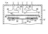
以下、添付図面を参照して、本発明の実施の形態について詳細に説明する。 図1は、本発明の一実施形態に係る成膜装置を示す断面図、図2はその内部の平面図である。ここではALD法を利用したCVD成膜装置によりTiN膜を成膜する場合について説明する。 Embodiments of the present invention will be described below in detail with reference to the accompanying drawings. FIG. 1 is a sectional view showing a film forming apparatus according to an embodiment of the present invention, and FIG. 2 is a plan view of the inside thereof. Here, a case where a TiN film is formed by a CVD film forming apparatus using the ALD method will be described.
このCVD成膜装置10は、真空引き可能に構成された略円筒状のチャンバー11を有しており、その中には被処理体であるウエハWを水平かつ円周状に4枚支持可能なウエハ支持部材12が設けられている。ウエハ支持部材12は、図2に示すように、4つのウエハ支持部12aを有しており、これらにウエハWが支持されるようになっている。また、ウエハ支持部材12の中心には下方に延びる回転軸13が設けられており、この回転軸13はモーター14の軸に取り付けられている。そして、このモーター14を回転させることにより、回転軸13を介してウエハ支持部材12が図2の矢印方向に沿って回転されるようになっている。したがって、ウエハ支持部12aに支持されたウエハWは、ウエハ支持部材12の回転によって回転軸13の回りを公転するようになっている。 The CVD
ウエハ支持部材12の下方には、ヒーター支持部材15が設けられており、このヒーター支持部材15には、ウエハWの移動軌跡に沿って内側および外側2つの円環状のヒーター16が支持されている。 A
チャンバー11の天壁11aには、第1の処理ガス吐出ノズル(第1の処理ガス吐出部)20および第2の処理ガス吐出ノズル(第2の処理ガス吐出部)21が、そのガス吐出口20a,21aをウエハ支持部材12の上面に対向させた状態で設けられている。これら第1の処理ガス吐出ノズル20および第2の処理ガス吐出ノズル21は、図2に示すように2つずつ、中心側から外周側に向かう径方向に沿って放射状に設けられており、これらは交互にウエハWの移動軌跡(ウエハ配置領域)に沿って円周状に配置されている。これら第1の処理ガス吐出ノズル20および第2の処理ガス吐出ノズル21は、チャンバー11の径方向に長く、チャンバー11の周方向に短い扁平状をなしており、径方向の長さが支持部材12に支持されたウエハWの直径(ウエハ配置領域の径方向の長さ)よりも長くなるように設けられている(図2参照)。また、隣接する第1の処理ガス吐出ノズル20および第2の処理ガス吐出ノズル21は回転軸13を中心として90°の角度で配置されている。また、チャンバー11の天壁11aには、4つのパージガス吐出ノズル(パージガス吐出部)22が隣接する第1の処理ガス吐出ノズル20および第2の処理ガス吐出ノズル21の間に位置するように設けられている。これら4つのパージガス吐出ノズル22はそれぞれ独立した状態で中心側から外周側に向けて放射状に設けられており、チャンバー11の径方向に長く、チャンバー11の周方向に短い扁平状をなしている。また、パージガス吐出ノズル22は、径方向の長さが支持部材12に支持されたウエハWの直径よりも長くなるように設けられている。 A first process gas discharge nozzle (first process gas discharge unit) 20 and a second process gas discharge nozzle (second process gas discharge unit) 21 are provided on the
図3(a)は第1の処理ガス吐出ノズル20および第2の処理ガス吐出ノズル21の断面図である。図3(a)に示すように、第1および第2の処理ガス吐出ノズル20,21は、それぞれ多数のガス吐出口20a,21aを有しており、この多数の吐出口20a,21aからチャンバー11内にシャワー状に処理ガスを吐出するように構成されている。また、図3(b)はパージガス吐出ノズル22の断面図である。図3(b)に示すように、パージガス吐出ノズル22の内部には多数の吐出口22aが設けられている。この多数の吐出口22aからは、ウエハ支持部材12に向けて直接ガスが吐出される。また、このパージガス吐出ノズル22は、多数の吐出口22aの下方に延びるように設けられたスカート部22bを有しており、吐出口22aからチャンバー11内にシャワー状にパージガスを吐出するとともに、スカート部22bによりシャワー状に吐出されたパージガスの流れが拡散することを防止しており、これによりパージガスのダウンフローがエアカーテンをなすように構成されている。そして、上述したように、パージガス吐出ノズル22は放射状に設けられ、その径方向の長さがウエハ支持部材12上のウエハWの長さよりも長いので、多数の吐出口22aも放射状にかつ支持部材12上のウエハWの長さよりも長い長さで分布し、吐出口22aから吐出されたパージガスのエアカーテンをウエハ支持部材12が通過する際に、その上のウエハWの全面がもれなくパージガスのエアカーテンを通過するようになる。すなわち、支持部材12上のウエハWを基準にすると、そのウエハW上をパージガスのエアカーテンが漏れなく走査可能となっている。このようなパージガスのエアカーテンにより、2つの処理ガスの分離性を高めることができる。 FIG. 3A is a cross-sectional view of the first process
また、パージガス吐出ノズル22のガス吐出口22aは、第1の処理ガス吐出ノズル20および第2の処理ガス吐出ノズル21のガス吐出口20a,21aよりも上方に設けられており、これにより第1の処理ガス雰囲気と第2の処理ガス雰囲気とをパージガスのエアカーテンにより分離可能になっている。これらノズル20,21,22からは、後述するガス供給機構30から所定のガスが供給されるようになっている。 Further, the
ガス供給機構30は、クリーニングガスとして、例えばClF3を供給するClF3供給源31、Arを供給するAr供給源32、TiCl4を供給するTiCl4供給源33、NH3を供給するNH3供給源34を有している。そして、ClF3供給源31にはClF3ガスライン35が、Ar供給源32にはArガスライン36が、TiCl4供給源33にはTiCl4ガスライン37が、NH3供給源34にはNH3ガスライン38がそれぞれ接続されている。そして、各ラインにはバルブ40およびマスフローコントローラ41が設けられている。
TiCl4供給源33から延びるTiCl4ガスライン37は、第1の処理ガス吐出ノズル20から延びるガス配管42に接続されている。また、TiCl4ガスライン37にはArガスライン36から延びる配管45が接続されており、ArガスにキャリアされたTiCl4ガスが配管42を通って第1の処理ガス吐出ノズル20から吐出される。また、NH3供給源34から延びるNH3ガスライン38は、第2の処理ガス吐出ノズル21から延びるガス配管43に接続されており、NH3ガスがNH3ガスライン38およびガス配管43を通って第2の処理ガス吐出ノズル21から吐出される。さらに、Ar供給源32から延びるArガスライン36は、パージガス吐出ノズル22から延びる配管44に接続されており、ArガスがArガスライン36および配管44を通ってパージガス吐出ノズル22から吐出される。さらにまた、ClF3供給源31から延びるClF3ガスライン35には、配管46,47,48が接続されており、これら配管46,47,48から配管42,43,44を介して第1の処理ガス吐出ノズル20、第2の処理ガス吐出ノズル21、およびパージガス吐出ノズル22からクリーニングガスであるClF3ガスを吐出可能となっている。なお、配管45,46,47,48には、それぞれバルブ45a,46a,47a,48aが設けられている。TiCl4 gas line 37 extending from the TiCl4 supply source 33 is connected to a
チャンバー11の底壁11bには、その中央部に排気口25が設けられており、この排気口25には排気管26が接続されている。この排気管26には排気装置28が接続されており、排気装置28を作動させることによりチャンバー11内を所定の真空度まで減圧することができる。 The
なお、排気管26は排気口25から垂直方向下方に延び途中で水平方向に屈曲しており、前記回転軸13は排気管26の垂直部の中を通って、排気管26の水平部の管壁を貫通して下方へ延びており、その管壁と回転軸13との間には、流体シール27が設けられている。 The
このように構成されたCVD成膜装置においては、まず、チャンバー11内に半導体ウエハWを装入し、ウエハ支持部材12のウエハ支持部12aにウエハWを載置する。次いで、ヒーター16よりウエハWを加熱しながらウエハ支持部材12を回転させ、排気装置28によりチャンバー11内を排気してチャンバー11内を所定の真空状態にする。引き続き、第1の処理ガス吐出ノズル20からArにキャリアさせたTiCl4ガスを、第2の処理ガス吐出ノズル21からNH3ガスを、パージガス吐出ノズル22からパージガスとしてのArガスをそれぞれ吐出させる。In the CVD film forming apparatus configured as described above, first, the semiconductor wafer W is loaded into the
ウエハ支持部材12のウエハ支持部12aのウエハWのうち、最初に第1の処理ガス吐出ノズル20から吐出されたTiCl4ガスが供給される2枚については、供給されたTiCl4ガスによりTiの単原子層が吸着した後、ウエハ支持部材12の回転により、パージガス吐出ノズル22から吐出されたArガスのエアカーテンを通過して、第2の処理ガス吐出ノズル21から吐出されたNH3ガスによりTiの単原子層の上にNの単原子層が堆積され、これらが反応してTiNが形成される。さらに、パージガス吐出ノズル22から吐出されたArガスのエアカーテンを通過した後、同様にしてTiの単原子層およびNの単原子層が供給され、これが所定回数繰り返されて所定厚さのTiN膜が形成される。また、最初に第2の処理ガス吐出ノズル21から吐出されたNH3ガスが供給される他の2枚については、供給されたNH3ガスによりNの単原子層が吸着した後、ウエハ支持部材12の回転により、パージガス吐出ノズル22から吐出されたArガスのエアカーテンを通過して、第1の処理ガス吐出ノズル20から吐出されたTiCl4ガスによりNの単原子層の上にTiの単原子層が堆積され、これらが反応してTiNが形成される。さらに、パージガス吐出ノズル22から吐出されたArガスのエアカーテンを通過した後、同様にしてNの単原子層およびTiの単原子層が供給され、これが所定回数繰り返されて所定厚さのTiN膜が形成される。この場合に、ウエハ支持部材12の回転速度は、処理ガスであるTiCl4ガスおよびNH3ガスの吸着速度に応じて決定される。Of the wafers W of the
また、この場合における第1の処理ガス吐出ノズル20および第2の処理ガス吐出ノズル21の形状およびウエハWとの間隔、さらにはガス流量は、ウエハWに均等に単原子層が吸着するような流れを形成することができるように設定される。また、パージガス吐出ノズル22とウエハWとの間隔、さらにはガス流量は、パージガスがTiCl4ガス雰囲気およびNH3ガス雰囲気を十分に分離可能なエアカーテンとして機能する流れを形成することができるように設定される。また、ヒーター16の加熱温度はTiとNとの反応に適した適宜の温度に設定される。以下、これらの設定値について具体的に述べる。In this case, the shape of the first process
図3(a)に示した構造を有する第1の処理ガス吐出ノズル20および第2の処理ガス吐出ノズル21は、吐出口20a,21aとその下方に位置する基板支持部材12に保持されたウエハW表面との間の距離h1が0.1〜10mmとなるように配置することができる。また、図3(b)に示した構造を有するパージガス吐出ノズル22は、吐出口22aとその下方に位置する基板支持部材12に保持されたウエハW表面との間の距離h2が0.1〜50mmとなるように配置することができ、その下端と基板支持部材12上面との間の距離h3が1.1〜50mmとなるように配置することができる。好ましくは、h1が0.1〜5mm、h2が0.2〜10mm、h3が1.2〜11mmとなるようにノズル20,21,22を配置する。The first processing
また、TiN成膜時におけるそれぞれのガス流量、チャンバー内圧力および加熱温度は、以下のように設定することができる。
TiCl4ガス流量:1〜50sccm(0.001〜0.05L/min)、好ましくは5〜20sccm(0.005〜0.02L/min)
Arガス(キャリアガス)流量:10〜100sccm(0.01〜0.1L/min)、TiCl4ガスが低流量の場合にはキャリアガスは用いなくてもよい
NH3ガス流量:50〜1000sccm(0.05〜1L/min)、好ましくは50〜500sccm(0.05〜0.5L/min)
パージガス流量:100〜1000sccm(0.1〜1L/min)
チャンバー内圧力:100mTorr〜5Torr(13.3Pa〜665Pa)、好ましくは100mTorr〜1Torr(13.3Pa〜133Pa)
加熱温度:300〜700℃、好ましくは400〜600℃Further, each gas flow rate, chamber internal pressure, and heating temperature during TiN film formation can be set as follows.
TiCl4 gas flow rate: 1 to 50 sccm (0.001 to 0.05 L / min), preferably 5 to 20 sccm (0.005 to 0.02 L / min)
Ar gas (carrier gas) flow rate: 10 to 100 sccm (0.01 to 0.1 L / min), carrier gas may not be used when the TiCl4 gas has a low flow rate NH3 gas flow rate: 50 to 1000 sccm ( 0.05 to 1 L / min), preferably 50 to 500 sccm (0.05 to 0.5 L / min)
Purge gas flow rate: 100 to 1000 sccm (0.1 to 1 L / min)
Pressure in chamber: 100 mTorr to 5 Torr (13.3 Pa to 665 Pa), preferably 100 mTorr to 1 Torr (13.3 Pa to 133 Pa)
Heating temperature: 300-700 ° C, preferably 400-600 ° C
以上のようにして、交互に配置された第1の処理ガス吐出ノズル20および第2の処理ガス吐出ノズル21からそれぞれTiCl4ガスおよびNH3ガスを供給しつつ、ウエハ支持部材12を回転させて、ウエハWにTiCl4ガスおよびNH3ガスを交互に供給するので、高速スイッチングバルブを用いることなく、ALD法によりTiの単原子層およびNの単原子層を交互に形成して所望のTiN膜を形成することができる。また、このようにウエハ支持部材12に複数枚のウエハWを載置し、一回の処理で複数枚の成膜処理を行うから、生産性が高い。また、パージガス吐出ノズル22からパージガスとしてのArガスを吐出してエアカーテンを形成することにより、TiCl4ガスおよびNH3ガスが混合することを極力防止することができ、また、パージガスであるArガスを吐出することにより、ウエハWの単原子層の形成が終了した部分の処理ガスを速やかに除去して余分な反応を防止することができるので、より良質の膜を形成することができる。As described above, the
このようなTiN膜の形成を繰り返し行い、所定枚数のウエハWの成膜処理が終了した時点で、ClF3源31からガスライン35、配管46,47,48および配管42,43,44を介してノズル20,21,22からClF3ガスを吐出させてチャンバー11内をクリーニングする。このとき、配管42,43,44やノズル20,21,22もクリーニングすることができる。When such a TiN film is repeatedly formed and the film forming process for a predetermined number of wafers W is completed, the ClF3 source 31 is connected to the
このクリーニング時におけるClF3ガス流量、チャンバー内圧力、クリーニング温度は、例えば以下に示すように設定することができる。
ClF3ガス流量:100〜500sccm(0.1〜0.5L/min)、好ましくは200〜300sccm(0.2〜0.3L/min)
チャンバー内圧力:1〜10Torr(133〜1330Pa)、好ましくは1〜5Torr(133〜665Pa)
クリーニング温度:200〜500℃、好ましくは200〜300℃The ClF3 gas flow rate, the pressure in the chamber, and the cleaning temperature during this cleaning can be set as shown below, for example.
ClF3 gas flow rate: 100 to 500 sccm (0.1 to 0.5 L / min), preferably 200 to 300 sccm (0.2 to 0.3 L / min)
Pressure in chamber: 1 to 10 Torr (133 to 1330 Pa), preferably 1 to 5 Torr (133 to 665 Pa)
Cleaning temperature: 200-500 ° C, preferably 200-300 ° C
次に、他の実施形態に係るCVD成膜装置について説明する。図4は他の実施形態に係るCVD成膜装置を部分的に示す断面図である。ここでは、ウエハ支持部材12の代わりにウエハ支持部材12’を用いてウエハWを自転させる構成となっている。すなわち、ウエハ支持部材12’は、ベース部材51の上に、4つ(図4では2つのみ図示)のウエハテーブル52が回転可能に設けられ、これらウエハテーブル52をモーター53により回転させることにより、ウエハテーブル52上のウエハWを自転させる。これにより、処理ガスとしてのTiCl4ガスおよびNH3ガスをより一層均一にウエハWに供給することができ、より均一な単原子層を形成することができる。この場合に、図1のようにヒーター16がウエハ支持部材の下にあると、加熱効率が悪くなるため、図4のようにウエハWの上方にヒーター16’を設けることが好ましい。15’はヒーター16’を支持するヒーター支持部材である。このようにヒーターを設けた場合には、処理ガスがウエハWに有効に供給されるようにヒーター16’およびヒーター支持部材15’にガス通過可能な多数の孔を設けることが好ましい。Next, a CVD film forming apparatus according to another embodiment will be described. FIG. 4 is a sectional view partially showing a CVD film forming apparatus according to another embodiment. Here, the wafer W is rotated using a
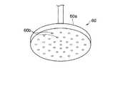
さらに、図5の実施形態では、処理ガスとしてのTiCl4ガスおよびNH3ガスをそれぞれシャワーヘッド60およびシャワーヘッド61から供給するようにしている。シャワーヘッド60は、図6に示すように、ディスク状をなす中空の本体60aの下面に多数のガス吐出孔60bが形成されており、このガス吐出孔60bから均一にガスを吐出する。シャワーヘッド61も同様に構成されている。このようにノズルの代わりにシャワーヘッドを用いることによってもウエハWに均一にTiCl4ガスおよびNH3ガスを供給することができる。Further, in the embodiment of FIG. 5, TiCl4 gas and NH3 gas as process gases are supplied from the
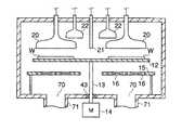
さらにまた、図7の実施形態では、第1の処理ガス吐出ノズル20および第2の処理ガス吐出ノズル21の直下に排気口70を設けている(第1の処理ガス吐出ノズル20に対応する排気口のみ図示)。このようにすることにより、不要なTiCl4ガスおよびNH3ガスを排気口70に接続された排気管71を介して速やかに排出することができる。Furthermore, in the embodiment of FIG. 7, an
なお、本発明は、上記実施の形態に限定されることなく種々変形可能である。例えば、上記実施形態では、TiN膜を成膜する例について示したが、Al2O3、ZrO2、TaN、SiO2、SiN、SiON、WN、WSi、RuO2等、他の金属化合物も同様にして成膜することができる。また、上記実施形態では、第1の処理ガスとしてTiCl4を用い、第2の処理ガスとしてNH3ガスを用いたが、第1の処理ガスと第2の処理ガスとは成膜する金属化合物膜に応じた適宜のガスを用いることができる。このような場合における第1の処理ガスとしては、TiCl4の他に、TaBr5、Ta(OC2H5)5、SiCl4、SiH4、Si2H6、SiH2Cl2、WF6等のAl、Zr、Ti、Ta、Si、WおよびRuのうち1種を含むものを挙げることができ、第2の処理ガスとしては、NH3の他に、NH3(N2)、O2、O3、NO、N2O、N2O3、N2O5等のNまたはOを含むものを挙げることができる。The present invention can be variously modified without being limited to the above embodiment. For example, in the above-described embodiment, an example in which a TiN film is formed has been described. However, other metal compounds such as Al2 O3 , ZrO2 , TaN, SiO2 , SiN, SiON, WN, WSi, and RuO2 are also the same. Thus, a film can be formed. In the above embodiment, TiCl4 is used as the first processing gas and NH3 gas is used as the second processing gas. However, the first processing gas and the second processing gas are metal compounds that form a film. An appropriate gas according to the film can be used. As the first processing gas in such a case, in addition to TiCl4 , TaBr5 , Ta (OC2 H5 )5 , SiCl4 , SiH4 , Si2 H6 , SiH2 Cl2 , WF6, etc. of Al, Zr, Ti, Ta, Si, can be mentioned those comprising one of W and Ru, as the second process gas, in additionto, NH3 (N 2) of NH3,O 2 , O3 , NO, N2 O, N2 O3 , N2 O5 and the like containing N or O.
また、ヒーターの位置を図1の例ではウエハの下方に、図4の例ではウエハの上方に設けたが、これら両方に設けてもよいし、均一に加熱することができれば他の位置に設けてもよい。さらに、パージガスとしてArガスを用いたが、N2ガス等他のガスであってもよい。また、2つの処理ガスを有効に遮断することができれば、パージガスを用いなくてもよい。さらにまた、用いる基板としては、半導体ウエハに限らず他のものであってもよく、また、表面上に他の層を形成した基板であってもよい。Further, although the heater is provided below the wafer in the example of FIG. 1 and above the wafer in the example of FIG. 4, it may be provided on both of them, or provided at other positions if uniform heating is possible. May be. Furthermore, although Ar gas is used as the purge gas, other gases such as N2 gas may be used. In addition, the purge gas may not be used as long as the two processing gases can be effectively shut off. Furthermore, the substrate to be used is not limited to a semiconductor wafer, and may be a substrate in which another layer is formed on the surface.
10;CVD成膜装置
11;チャンバー
12,12’;ウエハ支持部材
12a;ウエハ支持部
13;回転軸
14;モーター
16,16’;ヒーター
20,21;処理ガス吐出ノズル
22;パージガス吐出ノズル
30;ガス供給機構
25,70;排気口
26,71;排気管
28;排気装置
52;ウエハテーブル
53;モーター
60,61;シャワーヘッド
W;半導体ウエハDESCRIPTION OF
Claims (11)
Translated fromJapanese前記チャンバー内で複数の基板を平面的に支持する基板支持部材と、
前記チャンバー内に設けられ、第1の処理ガスを吐出する第1の処理ガス吐出部と、
前記チャンバー内の第1の処理ガス吐出部とは異なる位置に設けられ、第2の処理ガスを吐出する第2の処理ガス吐出部と、
前記チャンバー内にクリーニングガスを吐出するクリーニングガス吐出手段と、
前記基板支持部材を回転させる回転機構と、
前記基板を加熱する加熱手段と
を具備し、
前記基板支持部材を回転させながら、基板上に、第1の処理ガスおよび第2の処理ガスを交互に吸着させ、クリーニングガスにより前記チャンバー内をクリーニングすることを特徴とする成膜装置。A chamber for housing the substrate;
A substrate support member for planarly supporting a plurality of substrates in the chamber;
A first processing gas discharge section provided in the chamber and discharging a first processing gas;
A second processing gas discharge section that is provided at a position different from the first processing gas discharge section in the chamber and discharges a second processing gas;
Cleaning gas discharge means for discharging a cleaning gas into the chamber;
A rotation mechanism for rotating the substrate support member;
Heating means for heating the substrate,
A film forming apparatus, wherein the first support gas and the second process gas are alternately adsorbed onto the substrate while rotating the substrate support member, and the inside of the chamber is cleaned with a cleaning gas.
前記チャンバー内に第1の処理ガスを吐出する第1の処理ガス吐出部と第2の処理ガスを吐出する第2の処理ガス吐出部とを配置し、
前記基板支持部材を回転させながら、基板上に、第1の処理ガスおよび第2の処理ガスを交互に吸着させ、
膜形成終了後、クリーニングガス供給手段により前記チャンバー内にクリーニングガスを供給してクリーニングを行うことを特徴とする成膜方法。In a chamber, a plurality of substrates are supported in a state of being planarly arranged on a substrate support member,
A first processing gas discharge section for discharging a first processing gas and a second processing gas discharge section for discharging a second processing gas are disposed in the chamber;
While rotating the substrate support member, the first processing gas and the second processing gas are alternately adsorbed on the substrate,
After the film formation is completed, cleaning is performed by supplying a cleaning gas into the chamber by a cleaning gas supply means.
Priority Applications (1)
| Application Number | Priority Date | Filing Date | Title |
|---|---|---|---|
| JP2008089537AJP4817268B2 (en) | 2000-01-06 | 2008-03-31 | Film forming apparatus and film forming method |
Applications Claiming Priority (3)
| Application Number | Priority Date | Filing Date | Title |
|---|---|---|---|
| JP2000000590 | 2000-01-06 | ||
| JP2000000590 | 2000-01-06 | ||
| JP2008089537AJP4817268B2 (en) | 2000-01-06 | 2008-03-31 | Film forming apparatus and film forming method |
Related Parent Applications (1)
| Application Number | Title | Priority Date | Filing Date |
|---|---|---|---|
| JP2001000183ADivisionJP4817210B2 (en) | 2000-01-06 | 2001-01-04 | Film forming apparatus and film forming method |
Publications (3)
| Publication Number | Publication Date |
|---|---|
| JP2008190046Atrue JP2008190046A (en) | 2008-08-21 |
| JP2008190046A5 JP2008190046A5 (en) | 2011-02-03 |
| JP4817268B2 JP4817268B2 (en) | 2011-11-16 |
Family
ID=18529914
Family Applications (4)
| Application Number | Title | Priority Date | Filing Date |
|---|---|---|---|
| JP2008089537AExpired - Fee RelatedJP4817268B2 (en) | 2000-01-06 | 2008-03-31 | Film forming apparatus and film forming method |
| JP2008089538AWithdrawnJP2008208462A (en) | 2000-01-06 | 2008-03-31 | Film depositing apparatus and film depositing method |
| JP2008089536AExpired - Fee RelatedJP4817267B2 (en) | 2000-01-06 | 2008-03-31 | Film forming apparatus and film forming method |
| JP2008089535AExpired - Fee RelatedJP4817266B2 (en) | 2000-01-06 | 2008-03-31 | Film forming apparatus and film forming method |
Family Applications After (3)
| Application Number | Title | Priority Date | Filing Date |
|---|---|---|---|
| JP2008089538AWithdrawnJP2008208462A (en) | 2000-01-06 | 2008-03-31 | Film depositing apparatus and film depositing method |
| JP2008089536AExpired - Fee RelatedJP4817267B2 (en) | 2000-01-06 | 2008-03-31 | Film forming apparatus and film forming method |
| JP2008089535AExpired - Fee RelatedJP4817266B2 (en) | 2000-01-06 | 2008-03-31 | Film forming apparatus and film forming method |
Country Status (2)
| Country | Link |
|---|---|
| US (1) | US6576062B2 (en) |
| JP (4) | JP4817268B2 (en) |
Cited By (5)
| Publication number | Priority date | Publication date | Assignee | Title |
|---|---|---|---|---|
| JP2010153769A (en)* | 2008-11-19 | 2010-07-08 | Tokyo Electron Ltd | Substrate position sensing device, substrate position sensing method, film forming device, film forming method, program, and computer readable storage medium |
| WO2013146278A1 (en)* | 2012-03-30 | 2013-10-03 | 株式会社日立国際電気 | Semiconductor device manufacturing method, substrate processing method, and substrate processing apparatus |
| JP2019052339A (en)* | 2017-09-13 | 2019-04-04 | 東京エレクトロン株式会社 | Cleaning method of exhaust pipe |
| JP2019196545A (en)* | 2018-05-11 | 2019-11-14 | ウォニク アイピーエス カンパニー リミテッドWonik Ips Co.,Ltd. | Thin film formation method |
| JP2022133280A (en)* | 2017-10-27 | 2022-09-13 | アプライド マテリアルズ インコーポレイテッド | Treatment environment of signal wafer in accordance with space separation |
Families Citing this family (514)
| Publication number | Priority date | Publication date | Assignee | Title |
|---|---|---|---|---|
| US20020195056A1 (en)* | 2000-05-12 | 2002-12-26 | Gurtej Sandhu | Versatile atomic layer deposition apparatus |
| US6541353B1 (en)* | 2000-08-31 | 2003-04-01 | Micron Technology, Inc. | Atomic layer doping apparatus and method |
| JP2002367990A (en)* | 2001-06-04 | 2002-12-20 | Tokyo Electron Ltd | Method for manufacturing semiconductor device |
| JP3886424B2 (en)* | 2001-08-28 | 2007-02-28 | 鹿児島日本電気株式会社 | Substrate processing apparatus and method |
| US6932871B2 (en)* | 2002-04-16 | 2005-08-23 | Applied Materials, Inc. | Multi-station deposition apparatus and method |
| US6869641B2 (en)* | 2002-07-03 | 2005-03-22 | Unaxis Balzers Ltd. | Method and apparatus for ALD on a rotary susceptor |
| US20040058293A1 (en)* | 2002-08-06 | 2004-03-25 | Tue Nguyen | Assembly line processing system |
| US7153542B2 (en)* | 2002-08-06 | 2006-12-26 | Tegal Corporation | Assembly line processing method |
| KR100497748B1 (en)* | 2002-09-17 | 2005-06-29 | 주식회사 무한 | ALD equament and ALD methode |
| US6972055B2 (en)* | 2003-03-28 | 2005-12-06 | Finens Corporation | Continuous flow deposition system |
| US6703296B1 (en)* | 2003-04-17 | 2004-03-09 | Macronix International Co. Ltd. | Method for forming metal salicide |
| US20050011459A1 (en)* | 2003-07-15 | 2005-01-20 | Heng Liu | Chemical vapor deposition reactor |
| US20050178336A1 (en)* | 2003-07-15 | 2005-08-18 | Heng Liu | Chemical vapor deposition reactor having multiple inlets |
| US20050205210A1 (en)* | 2004-01-06 | 2005-09-22 | Devine Daniel J | Advanced multi-pressure workpiece processing |
| US7892357B2 (en)* | 2004-01-12 | 2011-02-22 | Axcelis Technologies, Inc. | Gas distribution plate assembly for plasma reactors |
| TWI334450B (en)* | 2004-03-12 | 2010-12-11 | Hitachi Int Electric Inc | Wafer treatment device and the manufacturing method of semiconductor device |
| KR100574569B1 (en)* | 2004-04-30 | 2006-05-03 | 주성엔지니어링(주) | Thin film deposition apparatus having thin film deposition method and separated purge gas injection hole |
| TWI249589B (en)* | 2004-07-16 | 2006-02-21 | Promos Technologies Inc | Method for improving atomic layer deposition process and the device thereof |
| CN100411117C (en)* | 2004-09-10 | 2008-08-13 | 茂德科技股份有限公司 | Method and apparatus for improving atomic layer deposition process |
| US20060137609A1 (en)* | 2004-09-13 | 2006-06-29 | Puchacz Jerzy P | Multi-single wafer processing apparatus |
| US20060073276A1 (en)* | 2004-10-04 | 2006-04-06 | Eric Antonissen | Multi-zone atomic layer deposition apparatus and method |
| KR100558922B1 (en)* | 2004-12-16 | 2006-03-10 | (주)퓨전에이드 | Thin film deposition apparatus and method |
| US20060195261A1 (en)* | 2005-02-10 | 2006-08-31 | Homeland Integrated Security Systems, Inc. | Electronic device for tracking and monitoring assets |
| BRPI0609695A2 (en) | 2005-03-21 | 2011-10-18 | Applera Corp | compound or a pharmaceutically acceptable salt thereof, pharmaceutical composition, and method for treating a disease and a patient undergoing therapy |
| CN100358098C (en) | 2005-08-05 | 2007-12-26 | 中微半导体设备(上海)有限公司 | Semiconductor arts piece processing device |
| WO2007075435A2 (en)* | 2005-12-15 | 2007-07-05 | Fluens Corporation | Apparatus for reactive sputtering |
| JP4760516B2 (en)* | 2005-12-15 | 2011-08-31 | 東京エレクトロン株式会社 | Coating apparatus and coating method |
| WO2007106076A2 (en)* | 2006-03-03 | 2007-09-20 | Prasad Gadgil | Apparatus and method for large area multi-layer atomic layer chemical vapor processing of thin films |
| US20070218702A1 (en)* | 2006-03-15 | 2007-09-20 | Asm Japan K.K. | Semiconductor-processing apparatus with rotating susceptor |
| US20070234956A1 (en)* | 2006-04-05 | 2007-10-11 | Dalton Jeremie J | Method and apparatus for providing uniform gas delivery to a reactor |
| WO2008011579A2 (en)* | 2006-07-21 | 2008-01-24 | Aixtron, Inc. | Small volume symmetric flow single wafer ald apparatus |
| US8187679B2 (en)* | 2006-07-29 | 2012-05-29 | Lotus Applied Technology, Llc | Radical-enhanced atomic layer deposition system and method |
| US20080057195A1 (en)* | 2006-08-31 | 2008-03-06 | United Technologies Corporation | Non-line of sight coating technique |
| KR20080027009A (en)* | 2006-09-22 | 2008-03-26 | 에이에스엠지니텍코리아 주식회사 | Atomic layer deposition apparatus and multilayer film deposition method using the same |
| US7879401B2 (en)* | 2006-12-22 | 2011-02-01 | The Regents Of The University Of Michigan | Organic vapor jet deposition using an exhaust |
| US8043432B2 (en)* | 2007-02-12 | 2011-10-25 | Tokyo Electron Limited | Atomic layer deposition systems and methods |
| US20080241384A1 (en)* | 2007-04-02 | 2008-10-02 | Asm Genitech Korea Ltd. | Lateral flow deposition apparatus and method of depositing film by using the apparatus |
| US8216419B2 (en)* | 2008-03-28 | 2012-07-10 | Bridgelux, Inc. | Drilled CVD shower head |
| US20090096349A1 (en)* | 2007-04-26 | 2009-04-16 | Moshtagh Vahid S | Cross flow cvd reactor |
| KR100830590B1 (en)* | 2007-06-01 | 2008-05-21 | 삼성전자주식회사 | Tungsten film, method for forming the same, method for forming a semiconductor device and its semiconductor device including the same |
| KR20090013286A (en)* | 2007-08-01 | 2009-02-05 | 삼성전자주식회사 | Semiconductor device manufacturing equipment |
| KR100918663B1 (en)* | 2007-08-22 | 2009-09-22 | 주식회사 테라세미콘 | Semiconductor manufacturing equipment |
| US8334015B2 (en)* | 2007-09-05 | 2012-12-18 | Intermolecular, Inc. | Vapor based combinatorial processing |
| DE102008010041A1 (en)* | 2007-09-28 | 2009-04-02 | Osram Opto Semiconductors Gmbh | Layer deposition apparatus, e.g. for epitaxial deposition of compound semiconductor layers, has segmented process gas enclosure in which substrate is moved relative to partition |
| EP2042619A3 (en) | 2007-09-28 | 2010-06-02 | OSRAM Opto Semiconductors GmbH | Coating apparatus and method for its operation |
| US8668775B2 (en)* | 2007-10-31 | 2014-03-11 | Toshiba Techno Center Inc. | Machine CVD shower head |
| US8282735B2 (en)* | 2007-11-27 | 2012-10-09 | Asm Genitech Korea Ltd. | Atomic layer deposition apparatus |
| CN101451237B (en)* | 2007-11-30 | 2012-02-08 | 中微半导体设备(上海)有限公司 | Plasma reaction chamber including multiple processing platforms having multiple plasma reaction zones |
| KR101394109B1 (en) | 2008-02-11 | 2014-05-13 | (주)소슬 | Substrate processing apparatus and Substrate processing system |
| US20100012036A1 (en)* | 2008-07-11 | 2010-01-21 | Hugo Silva | Isolation for multi-single-wafer processing apparatus |
| JP5423205B2 (en)* | 2008-08-29 | 2014-02-19 | 東京エレクトロン株式会社 | Deposition equipment |
| JP5276387B2 (en)* | 2008-09-04 | 2013-08-28 | 東京エレクトロン株式会社 | Film forming apparatus, substrate processing apparatus, film forming method, and recording medium recording program for executing this film forming method |
| JP5544697B2 (en)* | 2008-09-30 | 2014-07-09 | 東京エレクトロン株式会社 | Deposition equipment |
| US8426250B2 (en)* | 2008-10-22 | 2013-04-23 | Intel Corporation | Laser-assisted chemical singulation of a wafer |
| JP5445044B2 (en)* | 2008-11-14 | 2014-03-19 | 東京エレクトロン株式会社 | Deposition equipment |
| US10378106B2 (en) | 2008-11-14 | 2019-08-13 | Asm Ip Holding B.V. | Method of forming insulation film by modified PEALD |
| US20100129984A1 (en)* | 2008-11-26 | 2010-05-27 | George Vakanas | Wafer singulation in high volume manufacturing |
| DE102008062332A1 (en)* | 2008-12-15 | 2010-06-17 | Gühring Ohg | Device for surface treatment and / or coating of substrate components |
| US20100221426A1 (en)* | 2009-03-02 | 2010-09-02 | Fluens Corporation | Web Substrate Deposition System |
| JP5107285B2 (en)* | 2009-03-04 | 2012-12-26 | 東京エレクトロン株式会社 | Film forming apparatus, film forming method, program, and computer-readable storage medium |
| US20100227059A1 (en)* | 2009-03-04 | 2010-09-09 | Tokyo Electron Limited | Film deposition apparatus, film deposition method, and computer readable storage medium |
| US9394608B2 (en) | 2009-04-06 | 2016-07-19 | Asm America, Inc. | Semiconductor processing reactor and components thereof |
| JP5181100B2 (en)* | 2009-04-09 | 2013-04-10 | 東京エレクトロン株式会社 | Substrate processing apparatus, substrate processing method, and storage medium |
| JP5131240B2 (en)* | 2009-04-09 | 2013-01-30 | 東京エレクトロン株式会社 | Film forming apparatus, film forming method, and storage medium |
| US20110290175A1 (en)* | 2009-06-07 | 2011-12-01 | Veeco Instruments, Inc. | Multi-Chamber CVD Processing System |
| KR101110080B1 (en)* | 2009-07-08 | 2012-03-13 | 주식회사 유진테크 | Substrate treatment method for selectively inserting diffusion plate |
| JP5287592B2 (en)* | 2009-08-11 | 2013-09-11 | 東京エレクトロン株式会社 | Deposition equipment |
| US8802201B2 (en) | 2009-08-14 | 2014-08-12 | Asm America, Inc. | Systems and methods for thin-film deposition of metal oxides using excited nitrogen-oxygen species |
| JP5434484B2 (en)* | 2009-11-02 | 2014-03-05 | 東京エレクトロン株式会社 | Film forming apparatus, film forming method, and storage medium |
| JP5257328B2 (en)* | 2009-11-04 | 2013-08-07 | 東京エレクトロン株式会社 | Substrate processing apparatus, substrate processing method, and storage medium |
| JP5310512B2 (en)* | 2009-12-02 | 2013-10-09 | 東京エレクトロン株式会社 | Substrate processing equipment |
| JP5553588B2 (en)* | 2009-12-10 | 2014-07-16 | 東京エレクトロン株式会社 | Deposition equipment |
| JP5497423B2 (en)* | 2009-12-25 | 2014-05-21 | 東京エレクトロン株式会社 | Deposition equipment |
| US8034723B2 (en)* | 2009-12-25 | 2011-10-11 | Tokyo Electron Limited | Film deposition apparatus and film deposition method |
| JP5396264B2 (en)* | 2009-12-25 | 2014-01-22 | 東京エレクトロン株式会社 | Deposition equipment |
| JP5482196B2 (en)* | 2009-12-25 | 2014-04-23 | 東京エレクトロン株式会社 | Film forming apparatus, film forming method, and storage medium |
| KR101084184B1 (en) | 2010-01-11 | 2011-11-17 | 삼성모바일디스플레이주식회사 | Thin film deposition apparatus |
| US8741394B2 (en)* | 2010-03-25 | 2014-06-03 | Novellus Systems, Inc. | In-situ deposition of film stacks |
| JP5872141B2 (en)* | 2010-05-20 | 2016-03-01 | 東京エレクトロン株式会社 | Substrate processing apparatus, control apparatus and control method thereof |
| FI124113B (en)* | 2010-08-30 | 2014-03-31 | Beneq Oy | Apparatus and method for working the surface of a substrate |
| US8845806B2 (en)* | 2010-10-22 | 2014-09-30 | Asm Japan K.K. | Shower plate having different aperture dimensions and/or distributions |
| US20120225207A1 (en)* | 2011-03-01 | 2012-09-06 | Applied Materials, Inc. | Apparatus and Process for Atomic Layer Deposition |
| US20120222620A1 (en)* | 2011-03-01 | 2012-09-06 | Applied Materials, Inc. | Atomic Layer Deposition Carousel with Continuous Rotation and Methods of Use |
| US8541069B2 (en) | 2011-04-11 | 2013-09-24 | United Technologies Corporation | Method of guided non-line of sight coating |
| EP2518178B1 (en)* | 2011-04-29 | 2014-01-01 | Applied Materials, Inc. | Tooling carrier for inline coating machine, method of operating thereof and process of coating a substrate |
| US9312155B2 (en) | 2011-06-06 | 2016-04-12 | Asm Japan K.K. | High-throughput semiconductor-processing apparatus equipped with multiple dual-chamber modules |
| US9175392B2 (en)* | 2011-06-17 | 2015-11-03 | Intermolecular, Inc. | System for multi-region processing |
| US9793148B2 (en) | 2011-06-22 | 2017-10-17 | Asm Japan K.K. | Method for positioning wafers in multiple wafer transport |
| US10364496B2 (en) | 2011-06-27 | 2019-07-30 | Asm Ip Holding B.V. | Dual section module having shared and unshared mass flow controllers |
| US10854498B2 (en) | 2011-07-15 | 2020-12-01 | Asm Ip Holding B.V. | Wafer-supporting device and method for producing same |
| US20130023129A1 (en) | 2011-07-20 | 2013-01-24 | Asm America, Inc. | Pressure transmitter for a semiconductor processing environment |
| US8821641B2 (en)* | 2011-09-30 | 2014-09-02 | Samsung Electronics Co., Ltd. | Nozzle unit, and apparatus and method for treating substrate with the same |
| US9017481B1 (en) | 2011-10-28 | 2015-04-28 | Asm America, Inc. | Process feed management for semiconductor substrate processing |
| US20130192761A1 (en)* | 2012-01-31 | 2013-08-01 | Joseph Yudovsky | Rotary Substrate Processing System |
| US20130196078A1 (en)* | 2012-01-31 | 2013-08-01 | Joseph Yudovsky | Multi-Chamber Substrate Processing System |
| US8946830B2 (en) | 2012-04-04 | 2015-02-03 | Asm Ip Holdings B.V. | Metal oxide protective layer for a semiconductor device |
| US20130323422A1 (en)* | 2012-05-29 | 2013-12-05 | Applied Materials, Inc. | Apparatus for CVD and ALD with an Elongate Nozzle and Methods Of Use |
| KR102070400B1 (en)* | 2012-06-29 | 2020-01-28 | 주성엔지니어링(주) | Apparatus and method for processing substrate |
| JP6040609B2 (en)* | 2012-07-20 | 2016-12-07 | 東京エレクトロン株式会社 | Film forming apparatus and film forming method |
| US9558931B2 (en) | 2012-07-27 | 2017-01-31 | Asm Ip Holding B.V. | System and method for gas-phase sulfur passivation of a semiconductor surface |
| US9659799B2 (en) | 2012-08-28 | 2017-05-23 | Asm Ip Holding B.V. | Systems and methods for dynamic semiconductor process scheduling |
| US9021985B2 (en) | 2012-09-12 | 2015-05-05 | Asm Ip Holdings B.V. | Process gas management for an inductively-coupled plasma deposition reactor |
| US9324811B2 (en) | 2012-09-26 | 2016-04-26 | Asm Ip Holding B.V. | Structures and devices including a tensile-stressed silicon arsenic layer and methods of forming same |
| US10714315B2 (en) | 2012-10-12 | 2020-07-14 | Asm Ip Holdings B.V. | Semiconductor reaction chamber showerhead |
| US11043386B2 (en) | 2012-10-26 | 2021-06-22 | Applied Materials, Inc. | Enhanced spatial ALD of metals through controlled precursor mixing |
| US9230815B2 (en) | 2012-10-26 | 2016-01-05 | Appled Materials, Inc. | Methods for depositing fluorine/carbon-free conformal tungsten |
| US9640416B2 (en) | 2012-12-26 | 2017-05-02 | Asm Ip Holding B.V. | Single-and dual-chamber module-attachable wafer-handling chamber |
| US20160376700A1 (en) | 2013-02-01 | 2016-12-29 | Asm Ip Holding B.V. | System for treatment of deposition reactor |
| US9484191B2 (en) | 2013-03-08 | 2016-11-01 | Asm Ip Holding B.V. | Pulsed remote plasma method and system |
| US9589770B2 (en) | 2013-03-08 | 2017-03-07 | Asm Ip Holding B.V. | Method and systems for in-situ formation of intermediate reactive species |
| CN104103549B (en)* | 2013-04-07 | 2018-05-18 | 盛美半导体设备(上海)有限公司 | Semiconductor processing chamber |
| JP6134191B2 (en) | 2013-04-07 | 2017-05-24 | 村川 惠美 | Rotary semi-batch ALD equipment |
| US8993054B2 (en) | 2013-07-12 | 2015-03-31 | Asm Ip Holding B.V. | Method and system to reduce outgassing in a reaction chamber |
| US9018111B2 (en) | 2013-07-22 | 2015-04-28 | Asm Ip Holding B.V. | Semiconductor reaction chamber with plasma capabilities |
| KR102115337B1 (en)* | 2013-07-31 | 2020-05-26 | 주성엔지니어링(주) | Substrate processing apparatus |
| US9793115B2 (en) | 2013-08-14 | 2017-10-17 | Asm Ip Holding B.V. | Structures and devices including germanium-tin films and methods of forming same |
| JP6338462B2 (en)* | 2013-09-11 | 2018-06-06 | 東京エレクトロン株式会社 | Plasma processing equipment |
| KR101466816B1 (en)* | 2013-09-23 | 2014-12-10 | 국제엘렉트릭코리아 주식회사 | Heater member and substrate processing apparatus using sysceptor |
| US9240412B2 (en) | 2013-09-27 | 2016-01-19 | Asm Ip Holding B.V. | Semiconductor structure and device and methods of forming same using selective epitaxial process |
| US9556516B2 (en) | 2013-10-09 | 2017-01-31 | ASM IP Holding B.V | Method for forming Ti-containing film by PEALD using TDMAT or TDEAT |
| US9694436B2 (en)* | 2013-11-04 | 2017-07-04 | Veeco Precision Surface Processing Llc | System and method for flux coat, reflow and clean |
| US10179947B2 (en) | 2013-11-26 | 2019-01-15 | Asm Ip Holding B.V. | Method for forming conformal nitrided, oxidized, or carbonized dielectric film by atomic layer deposition |
| JP2017503079A (en)* | 2014-01-05 | 2017-01-26 | アプライド マテリアルズ インコーポレイテッドApplied Materials,Incorporated | Film deposition using spatial atomic layer deposition or pulsed chemical vapor deposition |
| JP6287240B2 (en)* | 2014-01-17 | 2018-03-07 | 東京エレクトロン株式会社 | Vacuum processing apparatus and vacuum processing method |
| US10683571B2 (en) | 2014-02-25 | 2020-06-16 | Asm Ip Holding B.V. | Gas supply manifold and method of supplying gases to chamber using same |
| US10167557B2 (en) | 2014-03-18 | 2019-01-01 | Asm Ip Holding B.V. | Gas distribution system, reactor including the system, and methods of using the same |
| US9447498B2 (en) | 2014-03-18 | 2016-09-20 | Asm Ip Holding B.V. | Method for performing uniform processing in gas system-sharing multiple reaction chambers |
| US11015245B2 (en) | 2014-03-19 | 2021-05-25 | Asm Ip Holding B.V. | Gas-phase reactor and system having exhaust plenum and components thereof |
| US9404587B2 (en) | 2014-04-24 | 2016-08-02 | ASM IP Holding B.V | Lockout tagout for semiconductor vacuum valve |
| US10858737B2 (en) | 2014-07-28 | 2020-12-08 | Asm Ip Holding B.V. | Showerhead assembly and components thereof |
| US9543180B2 (en) | 2014-08-01 | 2017-01-10 | Asm Ip Holding B.V. | Apparatus and method for transporting wafers between wafer carrier and process tool under vacuum |
| US9890456B2 (en) | 2014-08-21 | 2018-02-13 | Asm Ip Holding B.V. | Method and system for in situ formation of gas-phase compounds |
| WO2016043033A1 (en)* | 2014-09-17 | 2016-03-24 | 東京エレクトロン株式会社 | Shower head and deposition system |
| US9657845B2 (en) | 2014-10-07 | 2017-05-23 | Asm Ip Holding B.V. | Variable conductance gas distribution apparatus and method |
| US10941490B2 (en) | 2014-10-07 | 2021-03-09 | Asm Ip Holding B.V. | Multiple temperature range susceptor, assembly, reactor and system including the susceptor, and methods of using the same |
| JP6330623B2 (en)* | 2014-10-31 | 2018-05-30 | 東京エレクトロン株式会社 | Film forming apparatus, film forming method, and storage medium |
| JP6330630B2 (en)* | 2014-11-13 | 2018-05-30 | 東京エレクトロン株式会社 | Deposition equipment |
| KR102300403B1 (en) | 2014-11-19 | 2021-09-09 | 에이에스엠 아이피 홀딩 비.브이. | Method of depositing thin film |
| JP6404111B2 (en)* | 2014-12-18 | 2018-10-10 | 東京エレクトロン株式会社 | Plasma processing equipment |
| KR102263121B1 (en) | 2014-12-22 | 2021-06-09 | 에이에스엠 아이피 홀딩 비.브이. | Semiconductor device and manufacuring method thereof |
| US9478415B2 (en) | 2015-02-13 | 2016-10-25 | Asm Ip Holding B.V. | Method for forming film having low resistance and shallow junction depth |
| US10529542B2 (en) | 2015-03-11 | 2020-01-07 | Asm Ip Holdings B.V. | Cross-flow reactor and method |
| US9601391B2 (en)* | 2015-03-12 | 2017-03-21 | The United States Of America As Represented By The Administrator Of The National Aeronautics And Space Administration | Mechanical stress measurement during thin-film fabrication |
| US10276355B2 (en) | 2015-03-12 | 2019-04-30 | Asm Ip Holding B.V. | Multi-zone reactor, system including the reactor, and method of using the same |
| US10954597B2 (en)* | 2015-03-17 | 2021-03-23 | Asm Ip Holding B.V. | Atomic layer deposition apparatus |
| US10233528B2 (en) | 2015-06-08 | 2019-03-19 | Applied Materials, Inc. | Mask for deposition system and method for using the mask |
| US10458018B2 (en) | 2015-06-26 | 2019-10-29 | Asm Ip Holding B.V. | Structures including metal carbide material, devices including the structures, and methods of forming same |
| JP6447393B2 (en)* | 2015-07-06 | 2019-01-09 | 東京エレクトロン株式会社 | Film forming apparatus, film forming method, and storage medium |
| US10600673B2 (en) | 2015-07-07 | 2020-03-24 | Asm Ip Holding B.V. | Magnetic susceptor to baseplate seal |
| US10043661B2 (en) | 2015-07-13 | 2018-08-07 | Asm Ip Holding B.V. | Method for protecting layer by forming hydrocarbon-based extremely thin film |
| US9899291B2 (en) | 2015-07-13 | 2018-02-20 | Asm Ip Holding B.V. | Method for protecting layer by forming hydrocarbon-based extremely thin film |
| US10083836B2 (en) | 2015-07-24 | 2018-09-25 | Asm Ip Holding B.V. | Formation of boron-doped titanium metal films with high work function |
| US10087525B2 (en) | 2015-08-04 | 2018-10-02 | Asm Ip Holding B.V. | Variable gap hard stop design |
| US9647114B2 (en) | 2015-08-14 | 2017-05-09 | Asm Ip Holding B.V. | Methods of forming highly p-type doped germanium tin films and structures and devices including the films |
| KR20170022459A (en)* | 2015-08-20 | 2017-03-02 | 주성엔지니어링(주) | Substrate processing apparatus andsubstrate processing method |
| US9711345B2 (en) | 2015-08-25 | 2017-07-18 | Asm Ip Holding B.V. | Method for forming aluminum nitride-based film by PEALD |
| US9960072B2 (en) | 2015-09-29 | 2018-05-01 | Asm Ip Holding B.V. | Variable adjustment for precise matching of multiple chamber cavity housings |
| US9909214B2 (en) | 2015-10-15 | 2018-03-06 | Asm Ip Holding B.V. | Method for depositing dielectric film in trenches by PEALD |
| US11244822B2 (en) | 2015-10-20 | 2022-02-08 | Taiwan Semiconductor Manufacturing Co., Ltd. | Apparatus for manufacturing a thin film and a method therefor |
| US10211308B2 (en) | 2015-10-21 | 2019-02-19 | Asm Ip Holding B.V. | NbMC layers |
| US10322384B2 (en) | 2015-11-09 | 2019-06-18 | Asm Ip Holding B.V. | Counter flow mixer for process chamber |
| US9455138B1 (en) | 2015-11-10 | 2016-09-27 | Asm Ip Holding B.V. | Method for forming dielectric film in trenches by PEALD using H-containing gas |
| US9905420B2 (en) | 2015-12-01 | 2018-02-27 | Asm Ip Holding B.V. | Methods of forming silicon germanium tin films and structures and devices including the films |
| US9607837B1 (en) | 2015-12-21 | 2017-03-28 | Asm Ip Holding B.V. | Method for forming silicon oxide cap layer for solid state diffusion process |
| US9735024B2 (en) | 2015-12-28 | 2017-08-15 | Asm Ip Holding B.V. | Method of atomic layer etching using functional group-containing fluorocarbon |
| US9627221B1 (en) | 2015-12-28 | 2017-04-18 | Asm Ip Holding B.V. | Continuous process incorporating atomic layer etching |
| US11139308B2 (en) | 2015-12-29 | 2021-10-05 | Asm Ip Holding B.V. | Atomic layer deposition of III-V compounds to form V-NAND devices |
| US10529554B2 (en) | 2016-02-19 | 2020-01-07 | Asm Ip Holding B.V. | Method for forming silicon nitride film selectively on sidewalls or flat surfaces of trenches |
| US10468251B2 (en) | 2016-02-19 | 2019-11-05 | Asm Ip Holding B.V. | Method for forming spacers using silicon nitride film for spacer-defined multiple patterning |
| US9754779B1 (en) | 2016-02-19 | 2017-09-05 | Asm Ip Holding B.V. | Method for forming silicon nitride film selectively on sidewalls or flat surfaces of trenches |
| US10501866B2 (en) | 2016-03-09 | 2019-12-10 | Asm Ip Holding B.V. | Gas distribution apparatus for improved film uniformity in an epitaxial system |
| US10343920B2 (en) | 2016-03-18 | 2019-07-09 | Asm Ip Holding B.V. | Aligned carbon nanotubes |
| US9892913B2 (en) | 2016-03-24 | 2018-02-13 | Asm Ip Holding B.V. | Radial and thickness control via biased multi-port injection settings |
| TWI729101B (en) | 2016-04-02 | 2021-06-01 | 美商應用材料股份有限公司 | Apparatus and methods for wafer rotation in carousel susceptor |
| US10087522B2 (en) | 2016-04-21 | 2018-10-02 | Asm Ip Holding B.V. | Deposition of metal borides |
| US10190213B2 (en) | 2016-04-21 | 2019-01-29 | Asm Ip Holding B.V. | Deposition of metal borides |
| US10865475B2 (en) | 2016-04-21 | 2020-12-15 | Asm Ip Holding B.V. | Deposition of metal borides and silicides |
| TWI734770B (en) | 2016-04-24 | 2021-08-01 | 美商應用材料股份有限公司 | Apparatus for prevention of backside deposition in a spatial ald process chamber |
| US11015246B2 (en) | 2016-04-24 | 2021-05-25 | Applied Materials, Inc. | Apparatus and methods for depositing ALD films with enhanced chemical exchange |
| US10032628B2 (en) | 2016-05-02 | 2018-07-24 | Asm Ip Holding B.V. | Source/drain performance through conformal solid state doping |
| US10367080B2 (en) | 2016-05-02 | 2019-07-30 | Asm Ip Holding B.V. | Method of forming a germanium oxynitride film |
| KR102592471B1 (en) | 2016-05-17 | 2023-10-20 | 에이에스엠 아이피 홀딩 비.브이. | Method of forming metal interconnection and method of fabricating semiconductor device using the same |
| US11453943B2 (en) | 2016-05-25 | 2022-09-27 | Asm Ip Holding B.V. | Method for forming carbon-containing silicon/metal oxide or nitride film by ALD using silicon precursor and hydrocarbon precursor |
| US10388509B2 (en) | 2016-06-28 | 2019-08-20 | Asm Ip Holding B.V. | Formation of epitaxial layers via dislocation filtering |
| US10612137B2 (en) | 2016-07-08 | 2020-04-07 | Asm Ip Holdings B.V. | Organic reactants for atomic layer deposition |
| US9859151B1 (en) | 2016-07-08 | 2018-01-02 | Asm Ip Holding B.V. | Selective film deposition method to form air gaps |
| US9793135B1 (en) | 2016-07-14 | 2017-10-17 | ASM IP Holding B.V | Method of cyclic dry etching using etchant film |
| US10714385B2 (en) | 2016-07-19 | 2020-07-14 | Asm Ip Holding B.V. | Selective deposition of tungsten |
| KR102354490B1 (en) | 2016-07-27 | 2022-01-21 | 에이에스엠 아이피 홀딩 비.브이. | Method of processing a substrate |
| US10177025B2 (en) | 2016-07-28 | 2019-01-08 | Asm Ip Holding B.V. | Method and apparatus for filling a gap |
| KR102532607B1 (en) | 2016-07-28 | 2023-05-15 | 에이에스엠 아이피 홀딩 비.브이. | Substrate processing apparatus and method of operating the same |
| US9812320B1 (en) | 2016-07-28 | 2017-11-07 | Asm Ip Holding B.V. | Method and apparatus for filling a gap |
| US9887082B1 (en) | 2016-07-28 | 2018-02-06 | Asm Ip Holding B.V. | Method and apparatus for filling a gap |
| US10395919B2 (en) | 2016-07-28 | 2019-08-27 | Asm Ip Holding B.V. | Method and apparatus for filling a gap |
| US10090316B2 (en) | 2016-09-01 | 2018-10-02 | Asm Ip Holding B.V. | 3D stacked multilayer semiconductor memory using doped select transistor channel |
| US10410943B2 (en) | 2016-10-13 | 2019-09-10 | Asm Ip Holding B.V. | Method for passivating a surface of a semiconductor and related systems |
| US10643826B2 (en) | 2016-10-26 | 2020-05-05 | Asm Ip Holdings B.V. | Methods for thermally calibrating reaction chambers |
| US11532757B2 (en) | 2016-10-27 | 2022-12-20 | Asm Ip Holding B.V. | Deposition of charge trapping layers |
| US10714350B2 (en) | 2016-11-01 | 2020-07-14 | ASM IP Holdings, B.V. | Methods for forming a transition metal niobium nitride film on a substrate by atomic layer deposition and related semiconductor device structures |
| US10435790B2 (en) | 2016-11-01 | 2019-10-08 | Asm Ip Holding B.V. | Method of subatmospheric plasma-enhanced ALD using capacitively coupled electrodes with narrow gap |
| US10643904B2 (en) | 2016-11-01 | 2020-05-05 | Asm Ip Holdings B.V. | Methods for forming a semiconductor device and related semiconductor device structures |
| US10229833B2 (en) | 2016-11-01 | 2019-03-12 | Asm Ip Holding B.V. | Methods for forming a transition metal nitride film on a substrate by atomic layer deposition and related semiconductor device structures |
| US10134757B2 (en) | 2016-11-07 | 2018-11-20 | Asm Ip Holding B.V. | Method of processing a substrate and a device manufactured by using the method |
| KR102546317B1 (en) | 2016-11-15 | 2023-06-21 | 에이에스엠 아이피 홀딩 비.브이. | Gas supply unit and substrate processing apparatus including the same |
| US10340135B2 (en) | 2016-11-28 | 2019-07-02 | Asm Ip Holding B.V. | Method of topologically restricted plasma-enhanced cyclic deposition of silicon or metal nitride |
| KR102762543B1 (en) | 2016-12-14 | 2025-02-05 | 에이에스엠 아이피 홀딩 비.브이. | Substrate processing apparatus |
| US9916980B1 (en) | 2016-12-15 | 2018-03-13 | Asm Ip Holding B.V. | Method of forming a structure on a substrate |
| US11447861B2 (en) | 2016-12-15 | 2022-09-20 | Asm Ip Holding B.V. | Sequential infiltration synthesis apparatus and a method of forming a patterned structure |
| US11581186B2 (en) | 2016-12-15 | 2023-02-14 | Asm Ip Holding B.V. | Sequential infiltration synthesis apparatus |
| KR102700194B1 (en)* | 2016-12-19 | 2024-08-28 | 에이에스엠 아이피 홀딩 비.브이. | Substrate processing apparatus |
| US10269558B2 (en) | 2016-12-22 | 2019-04-23 | Asm Ip Holding B.V. | Method of forming a structure on a substrate |
| US10867788B2 (en) | 2016-12-28 | 2020-12-15 | Asm Ip Holding B.V. | Method of forming a structure on a substrate |
| US11390950B2 (en) | 2017-01-10 | 2022-07-19 | Asm Ip Holding B.V. | Reactor system and method to reduce residue buildup during a film deposition process |
| US10655221B2 (en) | 2017-02-09 | 2020-05-19 | Asm Ip Holding B.V. | Method for depositing oxide film by thermal ALD and PEALD |
| US10468261B2 (en) | 2017-02-15 | 2019-11-05 | Asm Ip Holding B.V. | Methods for forming a metallic film on a substrate by cyclical deposition and related semiconductor device structures |
| US10529563B2 (en) | 2017-03-29 | 2020-01-07 | Asm Ip Holdings B.V. | Method for forming doped metal oxide films on a substrate by cyclical deposition and related semiconductor device structures |
| US10283353B2 (en) | 2017-03-29 | 2019-05-07 | Asm Ip Holding B.V. | Method of reforming insulating film deposited on substrate with recess pattern |
| US10103040B1 (en) | 2017-03-31 | 2018-10-16 | Asm Ip Holding B.V. | Apparatus and method for manufacturing a semiconductor device |
| USD830981S1 (en) | 2017-04-07 | 2018-10-16 | Asm Ip Holding B.V. | Susceptor for semiconductor substrate processing apparatus |
| KR102457289B1 (en) | 2017-04-25 | 2022-10-21 | 에이에스엠 아이피 홀딩 비.브이. | Method for depositing a thin film and manufacturing a semiconductor device |
| US10446393B2 (en) | 2017-05-08 | 2019-10-15 | Asm Ip Holding B.V. | Methods for forming silicon-containing epitaxial layers and related semiconductor device structures |
| US10892156B2 (en) | 2017-05-08 | 2021-01-12 | Asm Ip Holding B.V. | Methods for forming a silicon nitride film on a substrate and related semiconductor device structures |
| US10770286B2 (en) | 2017-05-08 | 2020-09-08 | Asm Ip Holdings B.V. | Methods for selectively forming a silicon nitride film on a substrate and related semiconductor device structures |
| US10504742B2 (en) | 2017-05-31 | 2019-12-10 | Asm Ip Holding B.V. | Method of atomic layer etching using hydrogen plasma |
| US10886123B2 (en) | 2017-06-02 | 2021-01-05 | Asm Ip Holding B.V. | Methods for forming low temperature semiconductor layers and related semiconductor device structures |
| US12040200B2 (en) | 2017-06-20 | 2024-07-16 | Asm Ip Holding B.V. | Semiconductor processing apparatus and methods for calibrating a semiconductor processing apparatus |
| US11306395B2 (en)* | 2017-06-28 | 2022-04-19 | Asm Ip Holding B.V. | Methods for depositing a transition metal nitride film on a substrate by atomic layer deposition and related deposition apparatus |
| US10685834B2 (en) | 2017-07-05 | 2020-06-16 | Asm Ip Holdings B.V. | Methods for forming a silicon germanium tin layer and related semiconductor device structures |
| KR20190009245A (en) | 2017-07-18 | 2019-01-28 | 에이에스엠 아이피 홀딩 비.브이. | Methods for forming a semiconductor device structure and related semiconductor device structures |
| US10541333B2 (en) | 2017-07-19 | 2020-01-21 | Asm Ip Holding B.V. | Method for depositing a group IV semiconductor and related semiconductor device structures |
| US11374112B2 (en) | 2017-07-19 | 2022-06-28 | Asm Ip Holding B.V. | Method for depositing a group IV semiconductor and related semiconductor device structures |
| US11018002B2 (en) | 2017-07-19 | 2021-05-25 | Asm Ip Holding B.V. | Method for selectively depositing a Group IV semiconductor and related semiconductor device structures |
| US10590535B2 (en) | 2017-07-26 | 2020-03-17 | Asm Ip Holdings B.V. | Chemical treatment, deposition and/or infiltration apparatus and method for using the same |
| US10312055B2 (en) | 2017-07-26 | 2019-06-04 | Asm Ip Holding B.V. | Method of depositing film by PEALD using negative bias |
| US10605530B2 (en) | 2017-07-26 | 2020-03-31 | Asm Ip Holding B.V. | Assembly of a liner and a flange for a vertical furnace as well as the liner and the vertical furnace |
| TWI815813B (en) | 2017-08-04 | 2023-09-21 | 荷蘭商Asm智慧財產控股公司 | Showerhead assembly for distributing a gas within a reaction chamber |
| US10770336B2 (en) | 2017-08-08 | 2020-09-08 | Asm Ip Holding B.V. | Substrate lift mechanism and reactor including same |
| US10692741B2 (en) | 2017-08-08 | 2020-06-23 | Asm Ip Holdings B.V. | Radiation shield |
| US11769682B2 (en) | 2017-08-09 | 2023-09-26 | Asm Ip Holding B.V. | Storage apparatus for storing cassettes for substrates and processing apparatus equipped therewith |
| US10249524B2 (en) | 2017-08-09 | 2019-04-02 | Asm Ip Holding B.V. | Cassette holder assembly for a substrate cassette and holding member for use in such assembly |
| US11139191B2 (en) | 2017-08-09 | 2021-10-05 | Asm Ip Holding B.V. | Storage apparatus for storing cassettes for substrates and processing apparatus equipped therewith |
| US10236177B1 (en) | 2017-08-22 | 2019-03-19 | ASM IP Holding B.V.. | Methods for depositing a doped germanium tin semiconductor and related semiconductor device structures |
| USD900036S1 (en) | 2017-08-24 | 2020-10-27 | Asm Ip Holding B.V. | Heater electrical connector and adapter |
| US11830730B2 (en) | 2017-08-29 | 2023-11-28 | Asm Ip Holding B.V. | Layer forming method and apparatus |
| KR102491945B1 (en) | 2017-08-30 | 2023-01-26 | 에이에스엠 아이피 홀딩 비.브이. | Substrate processing apparatus |
| US11295980B2 (en) | 2017-08-30 | 2022-04-05 | Asm Ip Holding B.V. | Methods for depositing a molybdenum metal film over a dielectric surface of a substrate by a cyclical deposition process and related semiconductor device structures |
| US11056344B2 (en) | 2017-08-30 | 2021-07-06 | Asm Ip Holding B.V. | Layer forming method |
| KR102401446B1 (en) | 2017-08-31 | 2022-05-24 | 에이에스엠 아이피 홀딩 비.브이. | Substrate processing apparatus |
| US10607895B2 (en) | 2017-09-18 | 2020-03-31 | Asm Ip Holdings B.V. | Method for forming a semiconductor device structure comprising a gate fill metal |
| KR102630301B1 (en) | 2017-09-21 | 2024-01-29 | 에이에스엠 아이피 홀딩 비.브이. | Method of sequential infiltration synthesis treatment of infiltrateable material and structures and devices formed using same |
| US10844484B2 (en) | 2017-09-22 | 2020-11-24 | Asm Ip Holding B.V. | Apparatus for dispensing a vapor phase reactant to a reaction chamber and related methods |
| US10658205B2 (en) | 2017-09-28 | 2020-05-19 | Asm Ip Holdings B.V. | Chemical dispensing apparatus and methods for dispensing a chemical to a reaction chamber |
| US10403504B2 (en) | 2017-10-05 | 2019-09-03 | Asm Ip Holding B.V. | Method for selectively depositing a metallic film on a substrate |
| US10319588B2 (en) | 2017-10-10 | 2019-06-11 | Asm Ip Holding B.V. | Method for depositing a metal chalcogenide on a substrate by cyclical deposition |
| US10923344B2 (en) | 2017-10-30 | 2021-02-16 | Asm Ip Holding B.V. | Methods for forming a semiconductor structure and related semiconductor structures |
| US10910262B2 (en) | 2017-11-16 | 2021-02-02 | Asm Ip Holding B.V. | Method of selectively depositing a capping layer structure on a semiconductor device structure |
| KR102443047B1 (en) | 2017-11-16 | 2022-09-14 | 에이에스엠 아이피 홀딩 비.브이. | Method of processing a substrate and a device manufactured by the same |
| US11022879B2 (en) | 2017-11-24 | 2021-06-01 | Asm Ip Holding B.V. | Method of forming an enhanced unexposed photoresist layer |
| WO2019103613A1 (en) | 2017-11-27 | 2019-05-31 | Asm Ip Holding B.V. | A storage device for storing wafer cassettes for use with a batch furnace |
| CN111344522B (en) | 2017-11-27 | 2022-04-12 | 阿斯莫Ip控股公司 | Including clean mini-environment device |
| US10290508B1 (en) | 2017-12-05 | 2019-05-14 | Asm Ip Holding B.V. | Method for forming vertical spacers for spacer-defined patterning |
| US10760158B2 (en) | 2017-12-15 | 2020-09-01 | Lam Research Corporation | Ex situ coating of chamber components for semiconductor processing |
| US10872771B2 (en) | 2018-01-16 | 2020-12-22 | Asm Ip Holding B. V. | Method for depositing a material film on a substrate within a reaction chamber by a cyclical deposition process and related device structures |
| TWI799494B (en) | 2018-01-19 | 2023-04-21 | 荷蘭商Asm 智慧財產控股公司 | Deposition method |
| KR102695659B1 (en) | 2018-01-19 | 2024-08-14 | 에이에스엠 아이피 홀딩 비.브이. | Method for depositing a gap filling layer by plasma assisted deposition |
| USD903477S1 (en) | 2018-01-24 | 2020-12-01 | Asm Ip Holdings B.V. | Metal clamp |
| US11018047B2 (en) | 2018-01-25 | 2021-05-25 | Asm Ip Holding B.V. | Hybrid lift pin |
| USD880437S1 (en) | 2018-02-01 | 2020-04-07 | Asm Ip Holding B.V. | Gas supply plate for semiconductor manufacturing apparatus |
| US10535516B2 (en) | 2018-02-01 | 2020-01-14 | Asm Ip Holdings B.V. | Method for depositing a semiconductor structure on a surface of a substrate and related semiconductor structures |
| US11081345B2 (en) | 2018-02-06 | 2021-08-03 | Asm Ip Holding B.V. | Method of post-deposition treatment for silicon oxide film |
| US10896820B2 (en) | 2018-02-14 | 2021-01-19 | Asm Ip Holding B.V. | Method for depositing a ruthenium-containing film on a substrate by a cyclical deposition process |
| WO2019158960A1 (en) | 2018-02-14 | 2019-08-22 | Asm Ip Holding B.V. | A method for depositing a ruthenium-containing film on a substrate by a cyclical deposition process |
| US10731249B2 (en) | 2018-02-15 | 2020-08-04 | Asm Ip Holding B.V. | Method of forming a transition metal containing film on a substrate by a cyclical deposition process, a method for supplying a transition metal halide compound to a reaction chamber, and related vapor deposition apparatus |
| KR102636427B1 (en) | 2018-02-20 | 2024-02-13 | 에이에스엠 아이피 홀딩 비.브이. | Substrate processing method and apparatus |
| US10658181B2 (en) | 2018-02-20 | 2020-05-19 | Asm Ip Holding B.V. | Method of spacer-defined direct patterning in semiconductor fabrication |
| US10975470B2 (en) | 2018-02-23 | 2021-04-13 | Asm Ip Holding B.V. | Apparatus for detecting or monitoring for a chemical precursor in a high temperature environment |
| US11473195B2 (en) | 2018-03-01 | 2022-10-18 | Asm Ip Holding B.V. | Semiconductor processing apparatus and a method for processing a substrate |
| US11629406B2 (en) | 2018-03-09 | 2023-04-18 | Asm Ip Holding B.V. | Semiconductor processing apparatus comprising one or more pyrometers for measuring a temperature of a substrate during transfer of the substrate |
| US11114283B2 (en) | 2018-03-16 | 2021-09-07 | Asm Ip Holding B.V. | Reactor, system including the reactor, and methods of manufacturing and using same |
| KR102646467B1 (en) | 2018-03-27 | 2024-03-11 | 에이에스엠 아이피 홀딩 비.브이. | Method of forming an electrode on a substrate and a semiconductor device structure including an electrode |
| US10510536B2 (en) | 2018-03-29 | 2019-12-17 | Asm Ip Holding B.V. | Method of depositing a co-doped polysilicon film on a surface of a substrate within a reaction chamber |
| US11088002B2 (en) | 2018-03-29 | 2021-08-10 | Asm Ip Holding B.V. | Substrate rack and a substrate processing system and method |
| US11230766B2 (en) | 2018-03-29 | 2022-01-25 | Asm Ip Holding B.V. | Substrate processing apparatus and method |
| KR102501472B1 (en) | 2018-03-30 | 2023-02-20 | 에이에스엠 아이피 홀딩 비.브이. | Substrate processing method |
| KR102600229B1 (en) | 2018-04-09 | 2023-11-10 | 에이에스엠 아이피 홀딩 비.브이. | Substrate supporting device, substrate processing apparatus including the same and substrate processing method |
| US12025484B2 (en) | 2018-05-08 | 2024-07-02 | Asm Ip Holding B.V. | Thin film forming method |
| TWI811348B (en) | 2018-05-08 | 2023-08-11 | 荷蘭商Asm 智慧財產控股公司 | Methods for depositing an oxide film on a substrate by a cyclical deposition process and related device structures |
| US12272527B2 (en) | 2018-05-09 | 2025-04-08 | Asm Ip Holding B.V. | Apparatus for use with hydrogen radicals and method of using same |
| KR20190129718A (en) | 2018-05-11 | 2019-11-20 | 에이에스엠 아이피 홀딩 비.브이. | Methods for forming a doped metal carbide film on a substrate and related semiconductor device structures |
| KR102596988B1 (en) | 2018-05-28 | 2023-10-31 | 에이에스엠 아이피 홀딩 비.브이. | Method of processing a substrate and a device manufactured by the same |
| US11718913B2 (en) | 2018-06-04 | 2023-08-08 | Asm Ip Holding B.V. | Gas distribution system and reactor system including same |
| TWI840362B (en) | 2018-06-04 | 2024-05-01 | 荷蘭商Asm Ip私人控股有限公司 | Wafer handling chamber with moisture reduction |
| US11286562B2 (en) | 2018-06-08 | 2022-03-29 | Asm Ip Holding B.V. | Gas-phase chemical reactor and method of using same |
| US10797133B2 (en) | 2018-06-21 | 2020-10-06 | Asm Ip Holding B.V. | Method for depositing a phosphorus doped silicon arsenide film and related semiconductor device structures |
| KR102568797B1 (en) | 2018-06-21 | 2023-08-21 | 에이에스엠 아이피 홀딩 비.브이. | Substrate processing system |
| KR102854019B1 (en) | 2018-06-27 | 2025-09-02 | 에이에스엠 아이피 홀딩 비.브이. | Periodic deposition method for forming a metal-containing material and films and structures comprising the metal-containing material |
| TWI873894B (en) | 2018-06-27 | 2025-02-21 | 荷蘭商Asm Ip私人控股有限公司 | Cyclic deposition methods for forming metal-containing material and films and structures including the metal-containing material |
| US10612136B2 (en) | 2018-06-29 | 2020-04-07 | ASM IP Holding, B.V. | Temperature-controlled flange and reactor system including same |
| KR102686758B1 (en) | 2018-06-29 | 2024-07-18 | 에이에스엠 아이피 홀딩 비.브이. | Method for depositing a thin film and manufacturing a semiconductor device |
| US10755922B2 (en) | 2018-07-03 | 2020-08-25 | Asm Ip Holding B.V. | Method for depositing silicon-free carbon-containing film as gap-fill layer by pulse plasma-assisted deposition |
| US10388513B1 (en) | 2018-07-03 | 2019-08-20 | Asm Ip Holding B.V. | Method for depositing silicon-free carbon-containing film as gap-fill layer by pulse plasma-assisted deposition |
| US10767789B2 (en) | 2018-07-16 | 2020-09-08 | Asm Ip Holding B.V. | Diaphragm valves, valve components, and methods for forming valve components |
| US10483099B1 (en) | 2018-07-26 | 2019-11-19 | Asm Ip Holding B.V. | Method for forming thermally stable organosilicon polymer film |
| US11053591B2 (en) | 2018-08-06 | 2021-07-06 | Asm Ip Holding B.V. | Multi-port gas injection system and reactor system including same |
| US10883175B2 (en) | 2018-08-09 | 2021-01-05 | Asm Ip Holding B.V. | Vertical furnace for processing substrates and a liner for use therein |
| US10829852B2 (en) | 2018-08-16 | 2020-11-10 | Asm Ip Holding B.V. | Gas distribution device for a wafer processing apparatus |
| US11430674B2 (en) | 2018-08-22 | 2022-08-30 | Asm Ip Holding B.V. | Sensor array, apparatus for dispensing a vapor phase reactant to a reaction chamber and related methods |
| US11024523B2 (en) | 2018-09-11 | 2021-06-01 | Asm Ip Holding B.V. | Substrate processing apparatus and method |
| KR102707956B1 (en) | 2018-09-11 | 2024-09-19 | 에이에스엠 아이피 홀딩 비.브이. | Method for deposition of a thin film |
| US11049751B2 (en) | 2018-09-14 | 2021-06-29 | Asm Ip Holding B.V. | Cassette supply system to store and handle cassettes and processing apparatus equipped therewith |
| CN110970344B (en) | 2018-10-01 | 2024-10-25 | Asmip控股有限公司 | Substrate holding apparatus, system comprising the same and method of using the same |
| US11232963B2 (en) | 2018-10-03 | 2022-01-25 | Asm Ip Holding B.V. | Substrate processing apparatus and method |
| KR102592699B1 (en) | 2018-10-08 | 2023-10-23 | 에이에스엠 아이피 홀딩 비.브이. | Substrate support unit and apparatuses for depositing thin film and processing the substrate including the same |
| US10847365B2 (en) | 2018-10-11 | 2020-11-24 | Asm Ip Holding B.V. | Method of forming conformal silicon carbide film by cyclic CVD |
| US10811256B2 (en) | 2018-10-16 | 2020-10-20 | Asm Ip Holding B.V. | Method for etching a carbon-containing feature |
| KR20250110938A (en) | 2018-10-19 | 2025-07-21 | 램 리써치 코포레이션 | In situ protective coating of chamber components for semiconductor processing |
| KR102605121B1 (en) | 2018-10-19 | 2023-11-23 | 에이에스엠 아이피 홀딩 비.브이. | Substrate processing apparatus and substrate processing method |
| KR102546322B1 (en) | 2018-10-19 | 2023-06-21 | 에이에스엠 아이피 홀딩 비.브이. | Substrate processing apparatus and substrate processing method |
| USD948463S1 (en) | 2018-10-24 | 2022-04-12 | Asm Ip Holding B.V. | Susceptor for semiconductor substrate supporting apparatus |
| US10381219B1 (en) | 2018-10-25 | 2019-08-13 | Asm Ip Holding B.V. | Methods for forming a silicon nitride film |
| US12378665B2 (en) | 2018-10-26 | 2025-08-05 | Asm Ip Holding B.V. | High temperature coatings for a preclean and etch apparatus and related methods |
| US11087997B2 (en) | 2018-10-31 | 2021-08-10 | Asm Ip Holding B.V. | Substrate processing apparatus for processing substrates |
| KR102748291B1 (en) | 2018-11-02 | 2024-12-31 | 에이에스엠 아이피 홀딩 비.브이. | Substrate support unit and substrate processing apparatus including the same |
| US11572620B2 (en) | 2018-11-06 | 2023-02-07 | Asm Ip Holding B.V. | Methods for selectively depositing an amorphous silicon film on a substrate |
| US11031242B2 (en) | 2018-11-07 | 2021-06-08 | Asm Ip Holding B.V. | Methods for depositing a boron doped silicon germanium film |
| US10847366B2 (en) | 2018-11-16 | 2020-11-24 | Asm Ip Holding B.V. | Methods for depositing a transition metal chalcogenide film on a substrate by a cyclical deposition process |
| US10818758B2 (en) | 2018-11-16 | 2020-10-27 | Asm Ip Holding B.V. | Methods for forming a metal silicate film on a substrate in a reaction chamber and related semiconductor device structures |
| US10559458B1 (en) | 2018-11-26 | 2020-02-11 | Asm Ip Holding B.V. | Method of forming oxynitride film |
| US12040199B2 (en) | 2018-11-28 | 2024-07-16 | Asm Ip Holding B.V. | Substrate processing apparatus for processing substrates |
| US11217444B2 (en) | 2018-11-30 | 2022-01-04 | Asm Ip Holding B.V. | Method for forming an ultraviolet radiation responsive metal oxide-containing film |
| KR102636428B1 (en) | 2018-12-04 | 2024-02-13 | 에이에스엠 아이피 홀딩 비.브이. | A method for cleaning a substrate processing apparatus |
| US11158513B2 (en) | 2018-12-13 | 2021-10-26 | Asm Ip Holding B.V. | Methods for forming a rhenium-containing film on a substrate by a cyclical deposition process and related semiconductor device structures |
| TWI874340B (en) | 2018-12-14 | 2025-03-01 | 荷蘭商Asm Ip私人控股有限公司 | Method of forming device structure, structure formed by the method and system for performing the method |
| TWI866480B (en) | 2019-01-17 | 2024-12-11 | 荷蘭商Asm Ip 私人控股有限公司 | Methods of forming a transition metal containing film on a substrate by a cyclical deposition process |
| KR102727227B1 (en) | 2019-01-22 | 2024-11-07 | 에이에스엠 아이피 홀딩 비.브이. | Semiconductor processing device |
| CN111524788B (en) | 2019-02-01 | 2023-11-24 | Asm Ip私人控股有限公司 | Method for forming topologically selective films of silicon oxide |
| KR102626263B1 (en) | 2019-02-20 | 2024-01-16 | 에이에스엠 아이피 홀딩 비.브이. | Cyclical deposition method including treatment step and apparatus for same |
| TWI845607B (en) | 2019-02-20 | 2024-06-21 | 荷蘭商Asm Ip私人控股有限公司 | Cyclical deposition method and apparatus for filling a recess formed within a substrate surface |
| TWI873122B (en) | 2019-02-20 | 2025-02-21 | 荷蘭商Asm Ip私人控股有限公司 | Method of filling a recess formed within a surface of a substrate, semiconductor structure formed according to the method, and semiconductor processing apparatus |
| TWI838458B (en) | 2019-02-20 | 2024-04-11 | 荷蘭商Asm Ip私人控股有限公司 | Apparatus and methods for plug fill deposition in 3-d nand applications |
| TWI842826B (en) | 2019-02-22 | 2024-05-21 | 荷蘭商Asm Ip私人控股有限公司 | Substrate processing apparatus and method for processing substrate |
| US11742198B2 (en) | 2019-03-08 | 2023-08-29 | Asm Ip Holding B.V. | Structure including SiOCN layer and method of forming same |
| KR102858005B1 (en) | 2019-03-08 | 2025-09-09 | 에이에스엠 아이피 홀딩 비.브이. | Method for Selective Deposition of Silicon Nitride Layer and Structure Including Selectively-Deposited Silicon Nitride Layer |
| KR102782593B1 (en) | 2019-03-08 | 2025-03-14 | 에이에스엠 아이피 홀딩 비.브이. | Structure Including SiOC Layer and Method of Forming Same |
| JP2020167398A (en) | 2019-03-28 | 2020-10-08 | エーエスエム・アイピー・ホールディング・ベー・フェー | Door openers and substrate processing equipment provided with door openers |
| KR102809999B1 (en) | 2019-04-01 | 2025-05-19 | 에이에스엠 아이피 홀딩 비.브이. | Method of manufacturing semiconductor device |
| KR20200123380A (en) | 2019-04-19 | 2020-10-29 | 에이에스엠 아이피 홀딩 비.브이. | Layer forming method and apparatus |
| KR20200125453A (en) | 2019-04-24 | 2020-11-04 | 에이에스엠 아이피 홀딩 비.브이. | Gas-phase reactor system and method of using same |
| KR20200130121A (en) | 2019-05-07 | 2020-11-18 | 에이에스엠 아이피 홀딩 비.브이. | Chemical source vessel with dip tube |
| US11289326B2 (en) | 2019-05-07 | 2022-03-29 | Asm Ip Holding B.V. | Method for reforming amorphous carbon polymer film |
| KR20200130652A (en) | 2019-05-10 | 2020-11-19 | 에이에스엠 아이피 홀딩 비.브이. | Method of depositing material onto a surface and structure formed according to the method |
| JP7612342B2 (en) | 2019-05-16 | 2025-01-14 | エーエスエム・アイピー・ホールディング・ベー・フェー | Wafer boat handling apparatus, vertical batch furnace and method |
| JP7598201B2 (en) | 2019-05-16 | 2024-12-11 | エーエスエム・アイピー・ホールディング・ベー・フェー | Wafer boat handling apparatus, vertical batch furnace and method |
| USD975665S1 (en) | 2019-05-17 | 2023-01-17 | Asm Ip Holding B.V. | Susceptor shaft |
| USD947913S1 (en) | 2019-05-17 | 2022-04-05 | Asm Ip Holding B.V. | Susceptor shaft |
| USD935572S1 (en) | 2019-05-24 | 2021-11-09 | Asm Ip Holding B.V. | Gas channel plate |
| US10998209B2 (en) | 2019-05-31 | 2021-05-04 | Applied Materials, Inc. | Substrate processing platforms including multiple processing chambers |
| USD922229S1 (en) | 2019-06-05 | 2021-06-15 | Asm Ip Holding B.V. | Device for controlling a temperature of a gas supply unit |
| KR20200141002A (en) | 2019-06-06 | 2020-12-17 | 에이에스엠 아이피 홀딩 비.브이. | Method of using a gas-phase reactor system including analyzing exhausted gas |
| KR20200141931A (en) | 2019-06-10 | 2020-12-21 | 에이에스엠 아이피 홀딩 비.브이. | Method for cleaning quartz epitaxial chambers |
| KR20200143254A (en) | 2019-06-11 | 2020-12-23 | 에이에스엠 아이피 홀딩 비.브이. | Method of forming an electronic structure using an reforming gas, system for performing the method, and structure formed using the method |
| USD944946S1 (en) | 2019-06-14 | 2022-03-01 | Asm Ip Holding B.V. | Shower plate |
| USD931978S1 (en) | 2019-06-27 | 2021-09-28 | Asm Ip Holding B.V. | Showerhead vacuum transport |
| KR20210005515A (en) | 2019-07-03 | 2021-01-14 | 에이에스엠 아이피 홀딩 비.브이. | Temperature control assembly for substrate processing apparatus and method of using same |
| JP7499079B2 (en) | 2019-07-09 | 2024-06-13 | エーエスエム・アイピー・ホールディング・ベー・フェー | Plasma device using coaxial waveguide and substrate processing method |
| CN112216646A (en) | 2019-07-10 | 2021-01-12 | Asm Ip私人控股有限公司 | Substrate supporting assembly and substrate processing device comprising same |
| KR20210010307A (en) | 2019-07-16 | 2021-01-27 | 에이에스엠 아이피 홀딩 비.브이. | Substrate processing apparatus |
| KR20210010816A (en) | 2019-07-17 | 2021-01-28 | 에이에스엠 아이피 홀딩 비.브이. | Radical assist ignition plasma system and method |
| KR102860110B1 (en) | 2019-07-17 | 2025-09-16 | 에이에스엠 아이피 홀딩 비.브이. | Methods of forming silicon germanium structures |
| US11643724B2 (en) | 2019-07-18 | 2023-05-09 | Asm Ip Holding B.V. | Method of forming structures using a neutral beam |
| TWI839544B (en) | 2019-07-19 | 2024-04-21 | 荷蘭商Asm Ip私人控股有限公司 | Method of forming topology-controlled amorphous carbon polymer film |
| KR20210010817A (en) | 2019-07-19 | 2021-01-28 | 에이에스엠 아이피 홀딩 비.브이. | Method of Forming Topology-Controlled Amorphous Carbon Polymer Film |
| TWI851767B (en) | 2019-07-29 | 2024-08-11 | 荷蘭商Asm Ip私人控股有限公司 | Methods for selective deposition utilizing n-type dopants and/or alternative dopants to achieve high dopant incorporation |
| US12169361B2 (en) | 2019-07-30 | 2024-12-17 | Asm Ip Holding B.V. | Substrate processing apparatus and method |
| CN112309899A (en) | 2019-07-30 | 2021-02-02 | Asm Ip私人控股有限公司 | Substrate processing apparatus |
| CN112309900A (en) | 2019-07-30 | 2021-02-02 | Asm Ip私人控股有限公司 | Substrate processing apparatus |
| US11587815B2 (en) | 2019-07-31 | 2023-02-21 | Asm Ip Holding B.V. | Vertical batch furnace assembly |
| US11227782B2 (en) | 2019-07-31 | 2022-01-18 | Asm Ip Holding B.V. | Vertical batch furnace assembly |
| US11587814B2 (en) | 2019-07-31 | 2023-02-21 | Asm Ip Holding B.V. | Vertical batch furnace assembly |
| CN112323048B (en) | 2019-08-05 | 2024-02-09 | Asm Ip私人控股有限公司 | Liquid level sensor for chemical source container |
| CN112342526A (en) | 2019-08-09 | 2021-02-09 | Asm Ip私人控股有限公司 | Heater assembly including cooling device and method of using same |
| USD965524S1 (en) | 2019-08-19 | 2022-10-04 | Asm Ip Holding B.V. | Susceptor support |
| USD965044S1 (en) | 2019-08-19 | 2022-09-27 | Asm Ip Holding B.V. | Susceptor shaft |
| JP2021031769A (en) | 2019-08-21 | 2021-03-01 | エーエスエム アイピー ホールディング ビー.ブイ. | Production apparatus of mixed gas of film deposition raw material and film deposition apparatus |
| KR20210024423A (en) | 2019-08-22 | 2021-03-05 | 에이에스엠 아이피 홀딩 비.브이. | Method for forming a structure with a hole |
| USD930782S1 (en) | 2019-08-22 | 2021-09-14 | Asm Ip Holding B.V. | Gas distributor |
| USD979506S1 (en) | 2019-08-22 | 2023-02-28 | Asm Ip Holding B.V. | Insulator |
| USD940837S1 (en) | 2019-08-22 | 2022-01-11 | Asm Ip Holding B.V. | Electrode |
| USD949319S1 (en) | 2019-08-22 | 2022-04-19 | Asm Ip Holding B.V. | Exhaust duct |
| US11286558B2 (en) | 2019-08-23 | 2022-03-29 | Asm Ip Holding B.V. | Methods for depositing a molybdenum nitride film on a surface of a substrate by a cyclical deposition process and related semiconductor device structures including a molybdenum nitride film |
| KR20210024420A (en) | 2019-08-23 | 2021-03-05 | 에이에스엠 아이피 홀딩 비.브이. | Method for depositing silicon oxide film having improved quality by peald using bis(diethylamino)silane |
| KR102806450B1 (en) | 2019-09-04 | 2025-05-12 | 에이에스엠 아이피 홀딩 비.브이. | Methods for selective deposition using a sacrificial capping layer |
| KR102733104B1 (en) | 2019-09-05 | 2024-11-22 | 에이에스엠 아이피 홀딩 비.브이. | Substrate processing apparatus |
| US11562901B2 (en) | 2019-09-25 | 2023-01-24 | Asm Ip Holding B.V. | Substrate processing method |
| CN112593212B (en) | 2019-10-02 | 2023-12-22 | Asm Ip私人控股有限公司 | Method for forming topologically selective silicon oxide film by cyclic plasma enhanced deposition process |
| KR20210042810A (en) | 2019-10-08 | 2021-04-20 | 에이에스엠 아이피 홀딩 비.브이. | Reactor system including a gas distribution assembly for use with activated species and method of using same |
| TW202128273A (en) | 2019-10-08 | 2021-08-01 | 荷蘭商Asm Ip私人控股有限公司 | Gas injection system, reactor system, and method of depositing material on surface of substratewithin reaction chamber |
| TWI846953B (en) | 2019-10-08 | 2024-07-01 | 荷蘭商Asm Ip私人控股有限公司 | Substrate processing device |
| TWI846966B (en) | 2019-10-10 | 2024-07-01 | 荷蘭商Asm Ip私人控股有限公司 | Method of forming a photoresist underlayer and structure including same |
| US12009241B2 (en) | 2019-10-14 | 2024-06-11 | Asm Ip Holding B.V. | Vertical batch furnace assembly with detector to detect cassette |
| TWI834919B (en) | 2019-10-16 | 2024-03-11 | 荷蘭商Asm Ip私人控股有限公司 | Method of topology-selective film formation of silicon oxide |
| US11637014B2 (en) | 2019-10-17 | 2023-04-25 | Asm Ip Holding B.V. | Methods for selective deposition of doped semiconductor material |
| KR102845724B1 (en) | 2019-10-21 | 2025-08-13 | 에이에스엠 아이피 홀딩 비.브이. | Apparatus and methods for selectively etching films |
| KR20210050453A (en) | 2019-10-25 | 2021-05-07 | 에이에스엠 아이피 홀딩 비.브이. | Methods for filling a gap feature on a substrate surface and related semiconductor structures |
| US11646205B2 (en) | 2019-10-29 | 2023-05-09 | Asm Ip Holding B.V. | Methods of selectively forming n-type doped material on a surface, systems for selectively forming n-type doped material, and structures formed using same |
| KR20210054983A (en) | 2019-11-05 | 2021-05-14 | 에이에스엠 아이피 홀딩 비.브이. | Structures with doped semiconductor layers and methods and systems for forming same |
| US11501968B2 (en) | 2019-11-15 | 2022-11-15 | Asm Ip Holding B.V. | Method for providing a semiconductor device with silicon filled gaps |
| KR102861314B1 (en) | 2019-11-20 | 2025-09-17 | 에이에스엠 아이피 홀딩 비.브이. | Method of depositing carbon-containing material on a surface of a substrate, structure formed using the method, and system for forming the structure |
| CN112951697B (en) | 2019-11-26 | 2025-07-29 | Asmip私人控股有限公司 | Substrate processing apparatus |
| US11450529B2 (en) | 2019-11-26 | 2022-09-20 | Asm Ip Holding B.V. | Methods for selectively forming a target film on a substrate comprising a first dielectric surface and a second metallic surface |
| CN112885692B (en) | 2019-11-29 | 2025-08-15 | Asmip私人控股有限公司 | Substrate processing apparatus |
| CN120432376A (en) | 2019-11-29 | 2025-08-05 | Asm Ip私人控股有限公司 | Substrate processing apparatus |
| JP7527928B2 (en) | 2019-12-02 | 2024-08-05 | エーエスエム・アイピー・ホールディング・ベー・フェー | Substrate processing apparatus and substrate processing method |
| KR20210070898A (en) | 2019-12-04 | 2021-06-15 | 에이에스엠 아이피 홀딩 비.브이. | Substrate processing apparatus |
| KR20210078405A (en) | 2019-12-17 | 2021-06-28 | 에이에스엠 아이피 홀딩 비.브이. | Method of forming vanadium nitride layer and structure including the vanadium nitride layer |
| KR20210080214A (en) | 2019-12-19 | 2021-06-30 | 에이에스엠 아이피 홀딩 비.브이. | Methods for filling a gap feature on a substrate and related semiconductor structures |
| JP7730637B2 (en) | 2020-01-06 | 2025-08-28 | エーエスエム・アイピー・ホールディング・ベー・フェー | Gas delivery assembly, components thereof, and reactor system including same |
| JP7636892B2 (en) | 2020-01-06 | 2025-02-27 | エーエスエム・アイピー・ホールディング・ベー・フェー | Channeled Lift Pins |
| US11993847B2 (en) | 2020-01-08 | 2024-05-28 | Asm Ip Holding B.V. | Injector |
| KR20210093163A (en) | 2020-01-16 | 2021-07-27 | 에이에스엠 아이피 홀딩 비.브이. | Method of forming high aspect ratio features |
| KR102675856B1 (en) | 2020-01-20 | 2024-06-17 | 에이에스엠 아이피 홀딩 비.브이. | Method of forming thin film and method of modifying surface of thin film |
| TWI889744B (en) | 2020-01-29 | 2025-07-11 | 荷蘭商Asm Ip私人控股有限公司 | Contaminant trap system, and baffle plate stack |
| TW202513845A (en) | 2020-02-03 | 2025-04-01 | 荷蘭商Asm Ip私人控股有限公司 | Semiconductor structures and methods for forming the same |
| KR20210100010A (en) | 2020-02-04 | 2021-08-13 | 에이에스엠 아이피 홀딩 비.브이. | Method and apparatus for transmittance measurements of large articles |
| US11776846B2 (en) | 2020-02-07 | 2023-10-03 | Asm Ip Holding B.V. | Methods for depositing gap filling fluids and related systems and devices |
| KR20210103956A (en) | 2020-02-13 | 2021-08-24 | 에이에스엠 아이피 홀딩 비.브이. | Substrate processing apparatus including light receiving device and calibration method of light receiving device |
| TW202146691A (en) | 2020-02-13 | 2021-12-16 | 荷蘭商Asm Ip私人控股有限公司 | Gas distribution assembly, shower plate assembly, and method of adjusting conductance of gas to reaction chamber |
| TWI855223B (en) | 2020-02-17 | 2024-09-11 | 荷蘭商Asm Ip私人控股有限公司 | Method for growing phosphorous-doped silicon layer |
| CN113410160A (en) | 2020-02-28 | 2021-09-17 | Asm Ip私人控股有限公司 | System specially used for cleaning parts |
| KR20210113043A (en) | 2020-03-04 | 2021-09-15 | 에이에스엠 아이피 홀딩 비.브이. | Alignment fixture for a reactor system |
| KR20210116240A (en) | 2020-03-11 | 2021-09-27 | 에이에스엠 아이피 홀딩 비.브이. | Substrate handling device with adjustable joints |
| US11876356B2 (en) | 2020-03-11 | 2024-01-16 | Asm Ip Holding B.V. | Lockout tagout assembly and system and method of using same |
| KR102775390B1 (en) | 2020-03-12 | 2025-02-28 | 에이에스엠 아이피 홀딩 비.브이. | Method for Fabricating Layer Structure Having Target Topological Profile |
| US12173404B2 (en) | 2020-03-17 | 2024-12-24 | Asm Ip Holding B.V. | Method of depositing epitaxial material, structure formed using the method, and system for performing the method |
| KR102755229B1 (en) | 2020-04-02 | 2025-01-14 | 에이에스엠 아이피 홀딩 비.브이. | Thin film forming method |
| TWI887376B (en) | 2020-04-03 | 2025-06-21 | 荷蘭商Asm Ip私人控股有限公司 | Method for manufacturing semiconductor device |
| TWI888525B (en) | 2020-04-08 | 2025-07-01 | 荷蘭商Asm Ip私人控股有限公司 | Apparatus and methods for selectively etching silcon oxide films |
| KR20210127620A (en) | 2020-04-13 | 2021-10-22 | 에이에스엠 아이피 홀딩 비.브이. | method of forming a nitrogen-containing carbon film and system for performing the method |
| US11821078B2 (en) | 2020-04-15 | 2023-11-21 | Asm Ip Holding B.V. | Method for forming precoat film and method for forming silicon-containing film |
| KR20210128343A (en) | 2020-04-15 | 2021-10-26 | 에이에스엠 아이피 홀딩 비.브이. | Method of forming chromium nitride layer and structure including the chromium nitride layer |
| US11996289B2 (en) | 2020-04-16 | 2024-05-28 | Asm Ip Holding B.V. | Methods of forming structures including silicon germanium and silicon layers, devices formed using the methods, and systems for performing the methods |
| KR20210130646A (en) | 2020-04-21 | 2021-11-01 | 에이에스엠 아이피 홀딩 비.브이. | Method for processing a substrate |
| KR20210132600A (en) | 2020-04-24 | 2021-11-04 | 에이에스엠 아이피 홀딩 비.브이. | Methods and systems for depositing a layer comprising vanadium, nitrogen, and a further element |
| CN113555279A (en) | 2020-04-24 | 2021-10-26 | Asm Ip私人控股有限公司 | Methods of forming vanadium nitride-containing layers and structures comprising the same |
| TW202208671A (en) | 2020-04-24 | 2022-03-01 | 荷蘭商Asm Ip私人控股有限公司 | Methods of forming structures including vanadium boride and vanadium phosphide layers |
| KR102866804B1 (en) | 2020-04-24 | 2025-09-30 | 에이에스엠 아이피 홀딩 비.브이. | Vertical batch furnace assembly comprising a cooling gas supply |
| KR20210132612A (en) | 2020-04-24 | 2021-11-04 | 에이에스엠 아이피 홀딩 비.브이. | Methods and apparatus for stabilizing vanadium compounds |
| KR102783898B1 (en) | 2020-04-29 | 2025-03-18 | 에이에스엠 아이피 홀딩 비.브이. | Solid source precursor vessel |
| KR20210134869A (en) | 2020-05-01 | 2021-11-11 | 에이에스엠 아이피 홀딩 비.브이. | Fast FOUP swapping with a FOUP handler |
| JP7726664B2 (en) | 2020-05-04 | 2025-08-20 | エーエスエム・アイピー・ホールディング・ベー・フェー | Substrate processing system for processing a substrate |
| KR20210137395A (en) | 2020-05-07 | 2021-11-17 | 에이에스엠 아이피 홀딩 비.브이. | Apparatus and methods for performing an in-situ etch of reaction chambers with fluorine-based radicals |
| KR102788543B1 (en) | 2020-05-13 | 2025-03-27 | 에이에스엠 아이피 홀딩 비.브이. | Laser alignment fixture for a reactor system |
| TW202146699A (en) | 2020-05-15 | 2021-12-16 | 荷蘭商Asm Ip私人控股有限公司 | Method of forming a silicon germanium layer, semiconductor structure, semiconductor device, method of forming a deposition layer, and deposition system |
| KR20210143653A (en) | 2020-05-19 | 2021-11-29 | 에이에스엠 아이피 홀딩 비.브이. | Substrate processing apparatus |
| KR20210145079A (en) | 2020-05-21 | 2021-12-01 | 에이에스엠 아이피 홀딩 비.브이. | Flange and apparatus for processing substrates |
| KR102795476B1 (en) | 2020-05-21 | 2025-04-11 | 에이에스엠 아이피 홀딩 비.브이. | Structures including multiple carbon layers and methods of forming and using same |
| TWI873343B (en) | 2020-05-22 | 2025-02-21 | 荷蘭商Asm Ip私人控股有限公司 | Reaction system for forming thin film on substrate |
| KR20210146802A (en) | 2020-05-26 | 2021-12-06 | 에이에스엠 아이피 홀딩 비.브이. | Method for depositing boron and gallium containing silicon germanium layers |
| TWI876048B (en) | 2020-05-29 | 2025-03-11 | 荷蘭商Asm Ip私人控股有限公司 | Substrate processing device |
| TW202212620A (en) | 2020-06-02 | 2022-04-01 | 荷蘭商Asm Ip私人控股有限公司 | Apparatus for processing substrate, method of forming film, and method of controlling apparatus for processing substrate |
| TW202208659A (en) | 2020-06-16 | 2022-03-01 | 荷蘭商Asm Ip私人控股有限公司 | Method for depositing boron containing silicon germanium layers |
| TW202218133A (en) | 2020-06-24 | 2022-05-01 | 荷蘭商Asm Ip私人控股有限公司 | Method for forming a layer provided with silicon |
| TWI873359B (en) | 2020-06-30 | 2025-02-21 | 荷蘭商Asm Ip私人控股有限公司 | Substrate processing method |
| US12431354B2 (en) | 2020-07-01 | 2025-09-30 | Asm Ip Holding B.V. | Silicon nitride and silicon oxide deposition methods using fluorine inhibitor |
| TW202202649A (en) | 2020-07-08 | 2022-01-16 | 荷蘭商Asm Ip私人控股有限公司 | Substrate processing method |
| US12080571B2 (en) | 2020-07-08 | 2024-09-03 | Applied Materials, Inc. | Substrate processing module and method of moving a workpiece |
| KR20220010438A (en) | 2020-07-17 | 2022-01-25 | 에이에스엠 아이피 홀딩 비.브이. | Structures and methods for use in photolithography |
| TWI878570B (en) | 2020-07-20 | 2025-04-01 | 荷蘭商Asm Ip私人控股有限公司 | Method and system for depositing molybdenum layers |
| KR20220011092A (en) | 2020-07-20 | 2022-01-27 | 에이에스엠 아이피 홀딩 비.브이. | Method and system for forming structures including transition metal layers |
| US11817331B2 (en) | 2020-07-27 | 2023-11-14 | Applied Materials, Inc. | Substrate holder replacement with protective disk during pasting process |
| US11749542B2 (en) | 2020-07-27 | 2023-09-05 | Applied Materials, Inc. | Apparatus, system, and method for non-contact temperature monitoring of substrate supports |
| US12322591B2 (en) | 2020-07-27 | 2025-06-03 | Asm Ip Holding B.V. | Thin film deposition process |
| KR20220021863A (en) | 2020-08-14 | 2022-02-22 | 에이에스엠 아이피 홀딩 비.브이. | Method for processing a substrate |
| US12040177B2 (en) | 2020-08-18 | 2024-07-16 | Asm Ip Holding B.V. | Methods for forming a laminate film by cyclical plasma-enhanced deposition processes |
| TW202228863A (en) | 2020-08-25 | 2022-08-01 | 荷蘭商Asm Ip私人控股有限公司 | Method for cleaning a substrate, method for selectively depositing, and reaction system |
| US11725280B2 (en) | 2020-08-26 | 2023-08-15 | Asm Ip Holding B.V. | Method for forming metal silicon oxide and metal silicon oxynitride layers |
| TW202229601A (en) | 2020-08-27 | 2022-08-01 | 荷蘭商Asm Ip私人控股有限公司 | Method of forming patterned structures, method of manipulating mechanical property, device structure, and substrate processing system |
| US11600507B2 (en) | 2020-09-09 | 2023-03-07 | Applied Materials, Inc. | Pedestal assembly for a substrate processing chamber |
| TW202217045A (en) | 2020-09-10 | 2022-05-01 | 荷蘭商Asm Ip私人控股有限公司 | Methods for depositing gap filing fluids and related systems and devices |
| USD990534S1 (en) | 2020-09-11 | 2023-06-27 | Asm Ip Holding B.V. | Weighted lift pin |
| KR20220036866A (en) | 2020-09-16 | 2022-03-23 | 에이에스엠 아이피 홀딩 비.브이. | Silicon oxide deposition method |
| US11610799B2 (en) | 2020-09-18 | 2023-03-21 | Applied Materials, Inc. | Electrostatic chuck having a heating and chucking capabilities |
| USD1012873S1 (en) | 2020-09-24 | 2024-01-30 | Asm Ip Holding B.V. | Electrode for semiconductor processing apparatus |
| TWI889903B (en) | 2020-09-25 | 2025-07-11 | 荷蘭商Asm Ip私人控股有限公司 | Semiconductor processing method |
| US12009224B2 (en) | 2020-09-29 | 2024-06-11 | Asm Ip Holding B.V. | Apparatus and method for etching metal nitrides |
| KR20220045900A (en) | 2020-10-06 | 2022-04-13 | 에이에스엠 아이피 홀딩 비.브이. | Deposition method and an apparatus for depositing a silicon-containing material |
| CN114293174A (en) | 2020-10-07 | 2022-04-08 | Asm Ip私人控股有限公司 | Gas supply unit and substrate processing apparatus including the same |
| TW202229613A (en) | 2020-10-14 | 2022-08-01 | 荷蘭商Asm Ip私人控股有限公司 | Method of depositing material on stepped structure |
| TW202232565A (en) | 2020-10-15 | 2022-08-16 | 荷蘭商Asm Ip私人控股有限公司 | Method of manufacturing semiconductor device, and substrate treatment apparatus using ether-cat |
| TW202217037A (en) | 2020-10-22 | 2022-05-01 | 荷蘭商Asm Ip私人控股有限公司 | Method of depositing vanadium metal, structure, device and a deposition assembly |
| TW202223136A (en) | 2020-10-28 | 2022-06-16 | 荷蘭商Asm Ip私人控股有限公司 | Method for forming layer on substrate, and semiconductor processing system |
| TW202229620A (en) | 2020-11-12 | 2022-08-01 | 特文特大學 | Deposition system, method for controlling reaction condition, method for depositing |
| TW202229795A (en) | 2020-11-23 | 2022-08-01 | 荷蘭商Asm Ip私人控股有限公司 | A substrate processing apparatus with an injector |
| TW202235649A (en) | 2020-11-24 | 2022-09-16 | 荷蘭商Asm Ip私人控股有限公司 | Methods for filling a gap and related systems and devices |
| TW202235675A (en) | 2020-11-30 | 2022-09-16 | 荷蘭商Asm Ip私人控股有限公司 | Injector, and substrate processing apparatus |
| US12255053B2 (en) | 2020-12-10 | 2025-03-18 | Asm Ip Holding B.V. | Methods and systems for depositing a layer |
| TW202233884A (en) | 2020-12-14 | 2022-09-01 | 荷蘭商Asm Ip私人控股有限公司 | Method of forming structures for threshold voltage control |
| US11946137B2 (en) | 2020-12-16 | 2024-04-02 | Asm Ip Holding B.V. | Runout and wobble measurement fixtures |
| TW202232639A (en) | 2020-12-18 | 2022-08-16 | 荷蘭商Asm Ip私人控股有限公司 | Wafer processing apparatus with a rotatable table |
| TW202226899A (en) | 2020-12-22 | 2022-07-01 | 荷蘭商Asm Ip私人控股有限公司 | Plasma treatment device having matching box |
| TW202231903A (en) | 2020-12-22 | 2022-08-16 | 荷蘭商Asm Ip私人控股有限公司 | Transition metal deposition method, transition metal layer, and deposition assembly for depositing transition metal on substrate |
| TW202242184A (en) | 2020-12-22 | 2022-11-01 | 荷蘭商Asm Ip私人控股有限公司 | Precursor capsule, precursor vessel, vapor deposition assembly, and method of loading solid precursor into precursor vessel |
| US12195314B2 (en) | 2021-02-02 | 2025-01-14 | Applied Materials, Inc. | Cathode exchange mechanism to improve preventative maintenance time for cluster system |
| US11674227B2 (en) | 2021-02-03 | 2023-06-13 | Applied Materials, Inc. | Symmetric pump down mini-volume with laminar flow cavity gas injection for high and low pressure |
| USD980814S1 (en) | 2021-05-11 | 2023-03-14 | Asm Ip Holding B.V. | Gas distributor for substrate processing apparatus |
| USD1023959S1 (en) | 2021-05-11 | 2024-04-23 | Asm Ip Holding B.V. | Electrode for substrate processing apparatus |
| USD980813S1 (en) | 2021-05-11 | 2023-03-14 | Asm Ip Holding B.V. | Gas flow control plate for substrate processing apparatus |
| USD981973S1 (en) | 2021-05-11 | 2023-03-28 | Asm Ip Holding B.V. | Reactor wall for substrate processing apparatus |
| US12002668B2 (en) | 2021-06-25 | 2024-06-04 | Applied Materials, Inc. | Thermal management hardware for uniform temperature control for enhanced bake-out for cluster tool |
| USD990441S1 (en) | 2021-09-07 | 2023-06-27 | Asm Ip Holding B.V. | Gas flow control plate |
| JP7250085B2 (en)* | 2021-09-13 | 2023-03-31 | 株式会社Kokusai Electric | SUBSTRATE PROCESSING APPARATUS, SEMICONDUCTOR DEVICE MANUFACTURING METHOD AND PROGRAM |
| USD1060598S1 (en) | 2021-12-03 | 2025-02-04 | Asm Ip Holding B.V. | Split showerhead cover |
| JP7160421B1 (en) | 2022-02-10 | 2022-10-25 | 株式会社シー・ヴィ・リサーチ | Film forming apparatus, film forming method and gas nozzle |
| WO2025096387A1 (en)* | 2023-11-02 | 2025-05-08 | Applied Materials, Inc. | Multi-flow gas circuits, chamber kits, processing chambers, and related apparatus and methods for semiconductor manufacturing |
Citations (5)
| Publication number | Priority date | Publication date | Assignee | Title |
|---|---|---|---|---|
| JPS6226811A (en)* | 1985-07-26 | 1987-02-04 | Fujitsu Ltd | Semiconductor manufacturing equipment |
| JPH04287912A (en)* | 1991-02-19 | 1992-10-13 | Mitsubishi Electric Corp | Semiconductor manufacturing device |
| JPH05251701A (en)* | 1992-03-04 | 1993-09-28 | Fujitsu Ltd | Method of forming thin film transistor |
| JPH0786171A (en)* | 1993-09-17 | 1995-03-31 | Tokyo Electron Ltd | Batch cold wall processing system and leaning method therefor |
| JPH09330884A (en)* | 1996-06-07 | 1997-12-22 | Sony Corp | Epitaxial growth device |
Family Cites Families (28)
| Publication number | Priority date | Publication date | Assignee | Title |
|---|---|---|---|---|
| SE393967B (en)* | 1974-11-29 | 1977-05-31 | Sateko Oy | PROCEDURE AND PERFORMANCE OF LAYING BETWEEN THE STORAGE IN A LABOR PACKAGE |
| US4699805A (en)* | 1986-07-03 | 1987-10-13 | Motorola Inc. | Process and apparatus for the low pressure chemical vapor deposition of thin films |
| US4976996A (en)* | 1987-02-17 | 1990-12-11 | Lam Research Corporation | Chemical vapor deposition reactor and method of use thereof |
| JPS63266072A (en)* | 1987-04-23 | 1988-11-02 | Hitachi Electronics Eng Co Ltd | Gas phase reactor |
| JP2576135B2 (en)* | 1987-07-14 | 1997-01-29 | 日本電気株式会社 | Method of growing GaP crystal on Si substrate |
| US5166092A (en) | 1988-01-28 | 1992-11-24 | Fujitsu Limited | Method of growing compound semiconductor epitaxial layer by atomic layer epitaxy |
| WO1990010092A1 (en)* | 1989-02-24 | 1990-09-07 | Massachusetts Institute Of Technology | A modified stagnation flow apparatus for chemical vapor deposition providing excellent control of the deposition |
| JPH0824191B2 (en) | 1989-03-17 | 1996-03-06 | 富士通株式会社 | Thin film transistor |
| JP2940051B2 (en) | 1990-02-09 | 1999-08-25 | 富士通株式会社 | Method of forming insulating thin film |
| US5071670A (en)* | 1990-06-11 | 1991-12-10 | Kelly Michael A | Method for chemical vapor deposition under a single reactor vessel divided into separate reaction chambers each with its own depositing and exhausting means |
| US5225366A (en)* | 1990-06-22 | 1993-07-06 | The United States Of America As Represented By The Secretary Of The Navy | Apparatus for and a method of growing thin films of elemental semiconductors |
| JPH04236465A (en) | 1991-01-18 | 1992-08-25 | Fujitsu Ltd | Thin film transistor and its manufacturing method |
| JP3126787B2 (en) | 1992-01-30 | 2001-01-22 | 理化学研究所 | Film forming method and film forming apparatus |
| US5338362A (en)* | 1992-08-29 | 1994-08-16 | Tokyo Electron Limited | Apparatus for processing semiconductor wafer comprising continuously rotating wafer table and plural chamber compartments |
| JP3234025B2 (en) | 1993-02-24 | 2001-12-04 | 日本インテック株式会社 | Electrolyzed water generator |
| JP3144665B2 (en) | 1993-09-17 | 2001-03-12 | 東京エレクトロン株式会社 | Supply method of processing gas |
| US5647945A (en)* | 1993-08-25 | 1997-07-15 | Tokyo Electron Limited | Vacuum processing apparatus |
| DE19603323A1 (en)* | 1996-01-30 | 1997-08-07 | Siemens Ag | Method and device for producing SiC by CVD with improved gas utilization |
| TW340957B (en)* | 1996-02-01 | 1998-09-21 | Canon Hanbai Kk | Plasma processor and gas release device |
| US5747113A (en)* | 1996-07-29 | 1998-05-05 | Tsai; Charles Su-Chang | Method of chemical vapor deposition for producing layer variation by planetary susceptor rotation |
| US5807792A (en)* | 1996-12-18 | 1998-09-15 | Siemens Aktiengesellschaft | Uniform distribution of reactants in a device layer |
| US5879459A (en) | 1997-08-29 | 1999-03-09 | Genus, Inc. | Vertically-stacked process reactor and cluster tool system for atomic layer deposition |
| JP4114972B2 (en)* | 1997-05-27 | 2008-07-09 | キヤノンアネルバ株式会社 | Substrate processing equipment |
| US5951770A (en)* | 1997-06-04 | 1999-09-14 | Applied Materials, Inc. | Carousel wafer transfer system |
| US6020024A (en) | 1997-08-04 | 2000-02-01 | Motorola, Inc. | Method for forming high dielectric constant metal oxides |
| US6395640B2 (en)* | 1999-12-17 | 2002-05-28 | Texas Instruments Incorporated | Apparatus and method for selectivity restricting process fluid flow in semiconductor processing |
| US6143082A (en)* | 1998-10-08 | 2000-11-07 | Novellus Systems, Inc. | Isolation of incompatible processes in a multi-station processing chamber |
| KR100347379B1 (en) | 1999-05-01 | 2002-08-07 | 주식회사 피케이엘 | Atomic layer deposition apparatus for depositing multi substrate |
- 2001
- 2001-01-03USUS09/752,677patent/US6576062B2/ennot_activeExpired - Lifetime
- 2008
- 2008-03-31JPJP2008089537Apatent/JP4817268B2/ennot_activeExpired - Fee Related
- 2008-03-31JPJP2008089538Apatent/JP2008208462A/ennot_activeWithdrawn
- 2008-03-31JPJP2008089536Apatent/JP4817267B2/ennot_activeExpired - Fee Related
- 2008-03-31JPJP2008089535Apatent/JP4817266B2/ennot_activeExpired - Fee Related
Patent Citations (5)
| Publication number | Priority date | Publication date | Assignee | Title |
|---|---|---|---|---|
| JPS6226811A (en)* | 1985-07-26 | 1987-02-04 | Fujitsu Ltd | Semiconductor manufacturing equipment |
| JPH04287912A (en)* | 1991-02-19 | 1992-10-13 | Mitsubishi Electric Corp | Semiconductor manufacturing device |
| JPH05251701A (en)* | 1992-03-04 | 1993-09-28 | Fujitsu Ltd | Method of forming thin film transistor |
| JPH0786171A (en)* | 1993-09-17 | 1995-03-31 | Tokyo Electron Ltd | Batch cold wall processing system and leaning method therefor |
| JPH09330884A (en)* | 1996-06-07 | 1997-12-22 | Sony Corp | Epitaxial growth device |
Cited By (12)
| Publication number | Priority date | Publication date | Assignee | Title |
|---|---|---|---|---|
| JP2010153769A (en)* | 2008-11-19 | 2010-07-08 | Tokyo Electron Ltd | Substrate position sensing device, substrate position sensing method, film forming device, film forming method, program, and computer readable storage medium |
| WO2013146278A1 (en)* | 2012-03-30 | 2013-10-03 | 株式会社日立国際電気 | Semiconductor device manufacturing method, substrate processing method, and substrate processing apparatus |
| JPWO2013146278A1 (en)* | 2012-03-30 | 2015-12-10 | 株式会社日立国際電気 | Semiconductor device manufacturing method, substrate processing method, and substrate processing apparatus |
| US9546422B2 (en) | 2012-03-30 | 2017-01-17 | Hitachi Kokusai Electric Inc. | Semiconductor device manufacturing method and substrate processing method including a cleaning method |
| JP2019052339A (en)* | 2017-09-13 | 2019-04-04 | 東京エレクトロン株式会社 | Cleaning method of exhaust pipe |
| JP2022133280A (en)* | 2017-10-27 | 2022-09-13 | アプライド マテリアルズ インコーポレイテッド | Treatment environment of signal wafer in accordance with space separation |
| US11894257B2 (en) | 2017-10-27 | 2024-02-06 | Applied Materials, Inc. | Single wafer processing environments with spatial separation |
| JP7451601B2 (en) | 2017-10-27 | 2024-03-18 | アプライド マテリアルズ インコーポレイテッド | Single wafer processing environment with spatial separation |
| JP2024081654A (en)* | 2017-10-27 | 2024-06-18 | アプライド マテリアルズ インコーポレイテッド | Single wafer processing environment with spatial isolation |
| JP7749048B2 (en) | 2017-10-27 | 2025-10-03 | アプライド マテリアルズ インコーポレイテッド | Single wafer processing environment with spatial isolation |
| JP2019196545A (en)* | 2018-05-11 | 2019-11-14 | ウォニク アイピーエス カンパニー リミテッドWonik Ips Co.,Ltd. | Thin film formation method |
| JP7210864B2 (en) | 2018-05-11 | 2023-01-24 | ウォニク アイピーエス カンパニー リミテッド | Thin film forming method |
Also Published As
| Publication number | Publication date |
|---|---|
| US6576062B2 (en) | 2003-06-10 |
| JP2008208462A (en) | 2008-09-11 |
| JP2008190045A (en) | 2008-08-21 |
| JP4817266B2 (en) | 2011-11-16 |
| JP4817268B2 (en) | 2011-11-16 |
| US20010007244A1 (en) | 2001-07-12 |
| JP2008240154A (en) | 2008-10-09 |
| JP4817267B2 (en) | 2011-11-16 |
Similar Documents
| Publication | Publication Date | Title |
|---|---|---|
| JP4817267B2 (en) | Film forming apparatus and film forming method | |
| JP4817210B2 (en) | Film forming apparatus and film forming method | |
| US7763115B2 (en) | Vacuum film-forming apparatus | |
| JP5482196B2 (en) | Film forming apparatus, film forming method, and storage medium | |
| JP5780062B2 (en) | Substrate processing apparatus and film forming apparatus | |
| JP2008190046A5 (en) | ||
| KR102180823B1 (en) | Selective film forming method and method of manufacturing semiconductor device | |
| JP7345410B2 (en) | Film-forming method and film-forming equipment | |
| US20050241580A1 (en) | Method for depositing thin film and thin film deposition system having separate jet orifices for spraying purge gas | |
| JP2018059173A (en) | Deposition method | |
| KR101862907B1 (en) | Film forming method | |
| US20210249265A1 (en) | Deposition method and deposition apparatus | |
| JP2018186236A (en) | Substrate processing apparatus, exhaust pipe coating method, and substrate processing method | |
| KR101485506B1 (en) | Method for depositing thin film on wafer | |
| JP6971887B2 (en) | Film formation method and film formation equipment | |
| WO2022080153A1 (en) | Substrate processing method and substrate processing apparatus | |
| JP6910118B2 (en) | Film formation method and film formation system, and surface treatment method | |
| JP2022049557A (en) | Plasma purge method | |
| JP2004277772A (en) | Treatment device | |
| JP6544232B2 (en) | Film forming method and film forming apparatus | |
| CN112391612B (en) | Film forming method and film forming apparatus | |
| JP7243521B2 (en) | Film forming method and film forming apparatus | |
| JP7279605B2 (en) | Deposition apparatus and operation method of the deposition apparatus | |
| TWI576461B (en) | Thin film deposition method | |
| JP2006307303A (en) | Deposition equipment |
Legal Events
| Date | Code | Title | Description |
|---|---|---|---|
| A521 | Written amendment | Free format text:JAPANESE INTERMEDIATE CODE: A821 Effective date:20080501 | |
| A521 | Written amendment | Free format text:JAPANESE INTERMEDIATE CODE: A523 Effective date:20101210 | |
| A977 | Report on retrieval | Free format text:JAPANESE INTERMEDIATE CODE: A971007 Effective date:20110414 | |
| A131 | Notification of reasons for refusal | Free format text:JAPANESE INTERMEDIATE CODE: A131 Effective date:20110524 | |
| A521 | Written amendment | Free format text:JAPANESE INTERMEDIATE CODE: A523 Effective date:20110721 | |
| TRDD | Decision of grant or rejection written | ||
| A01 | Written decision to grant a patent or to grant a registration (utility model) | Free format text:JAPANESE INTERMEDIATE CODE: A01 Effective date:20110824 | |
| A01 | Written decision to grant a patent or to grant a registration (utility model) | Free format text:JAPANESE INTERMEDIATE CODE: A01 | |
| A61 | First payment of annual fees (during grant procedure) | Free format text:JAPANESE INTERMEDIATE CODE: A61 Effective date:20110824 | |
| FPAY | Renewal fee payment (event date is renewal date of database) | Free format text:PAYMENT UNTIL: 20140909 Year of fee payment:3 | |
| R150 | Certificate of patent or registration of utility model | Free format text:JAPANESE INTERMEDIATE CODE: R150 | |
| R250 | Receipt of annual fees | Free format text:JAPANESE INTERMEDIATE CODE: R250 | |
| LAPS | Cancellation because of no payment of annual fees |