JP2008181109A - Liquid crystal display device and electronic equipment using the same - Google Patents
Liquid crystal display device and electronic equipment using the sameDownload PDFInfo
- Publication number
- JP2008181109A JP2008181109AJP2007328123AJP2007328123AJP2008181109AJP 2008181109 AJP2008181109 AJP 2008181109AJP 2007328123 AJP2007328123 AJP 2007328123AJP 2007328123 AJP2007328123 AJP 2007328123AJP 2008181109 AJP2008181109 AJP 2008181109A
- Authority
- JP
- Japan
- Prior art keywords
- liquid crystal
- photoelectric conversion
- light
- conversion device
- pixel
- Prior art date
- Legal status (The legal status is an assumption and is not a legal conclusion. Google has not performed a legal analysis and makes no representation as to the accuracy of the status listed.)
- Withdrawn
Links
Images


Classifications
- G—PHYSICS
- G02—OPTICS
- G02F—OPTICAL DEVICES OR ARRANGEMENTS FOR THE CONTROL OF LIGHT BY MODIFICATION OF THE OPTICAL PROPERTIES OF THE MEDIA OF THE ELEMENTS INVOLVED THEREIN; NON-LINEAR OPTICS; FREQUENCY-CHANGING OF LIGHT; OPTICAL LOGIC ELEMENTS; OPTICAL ANALOGUE/DIGITAL CONVERTERS
- G02F1/00—Devices or arrangements for the control of the intensity, colour, phase, polarisation or direction of light arriving from an independent light source, e.g. switching, gating or modulating; Non-linear optics
- G02F1/01—Devices or arrangements for the control of the intensity, colour, phase, polarisation or direction of light arriving from an independent light source, e.g. switching, gating or modulating; Non-linear optics for the control of the intensity, phase, polarisation or colour
- G02F1/13—Devices or arrangements for the control of the intensity, colour, phase, polarisation or direction of light arriving from an independent light source, e.g. switching, gating or modulating; Non-linear optics for the control of the intensity, phase, polarisation or colour based on liquid crystals, e.g. single liquid crystal display cells
- G02F1/133—Constructional arrangements; Operation of liquid crystal cells; Circuit arrangements
- G02F1/13306—Circuit arrangements or driving methods for the control of single liquid crystal cells
- G02F1/13318—Circuits comprising a photodetector
- G—PHYSICS
- G09—EDUCATION; CRYPTOGRAPHY; DISPLAY; ADVERTISING; SEALS
- G09G—ARRANGEMENTS OR CIRCUITS FOR CONTROL OF INDICATING DEVICES USING STATIC MEANS TO PRESENT VARIABLE INFORMATION
- G09G3/00—Control arrangements or circuits, of interest only in connection with visual indicators other than cathode-ray tubes
- G09G3/20—Control arrangements or circuits, of interest only in connection with visual indicators other than cathode-ray tubes for presentation of an assembly of a number of characters, e.g. a page, by composing the assembly by combination of individual elements arranged in a matrix no fixed position being assigned to or needed to be assigned to the individual characters or partial characters
- G09G3/34—Control arrangements or circuits, of interest only in connection with visual indicators other than cathode-ray tubes for presentation of an assembly of a number of characters, e.g. a page, by composing the assembly by combination of individual elements arranged in a matrix no fixed position being assigned to or needed to be assigned to the individual characters or partial characters by control of light from an independent source
- G09G3/3406—Control of illumination source
- G—PHYSICS
- G09—EDUCATION; CRYPTOGRAPHY; DISPLAY; ADVERTISING; SEALS
- G09G—ARRANGEMENTS OR CIRCUITS FOR CONTROL OF INDICATING DEVICES USING STATIC MEANS TO PRESENT VARIABLE INFORMATION
- G09G2320/00—Control of display operating conditions
- G09G2320/06—Adjustment of display parameters
- G09G2320/0626—Adjustment of display parameters for control of overall brightness
- G09G2320/0633—Adjustment of display parameters for control of overall brightness by amplitude modulation of the brightness of the illumination source
- G—PHYSICS
- G09—EDUCATION; CRYPTOGRAPHY; DISPLAY; ADVERTISING; SEALS
- G09G—ARRANGEMENTS OR CIRCUITS FOR CONTROL OF INDICATING DEVICES USING STATIC MEANS TO PRESENT VARIABLE INFORMATION
- G09G2330/00—Aspects of power supply; Aspects of display protection and defect management
- G09G2330/02—Details of power systems and of start or stop of display operation
- G09G2330/021—Power management, e.g. power saving
- G—PHYSICS
- G09—EDUCATION; CRYPTOGRAPHY; DISPLAY; ADVERTISING; SEALS
- G09G—ARRANGEMENTS OR CIRCUITS FOR CONTROL OF INDICATING DEVICES USING STATIC MEANS TO PRESENT VARIABLE INFORMATION
- G09G2360/00—Aspects of the architecture of display systems
- G09G2360/14—Detecting light within display terminals, e.g. using a single or a plurality of photosensors
- G09G2360/144—Detecting light within display terminals, e.g. using a single or a plurality of photosensors the light being ambient light
Landscapes
- Physics & Mathematics (AREA)
- Nonlinear Science (AREA)
- Engineering & Computer Science (AREA)
- General Physics & Mathematics (AREA)
- Optics & Photonics (AREA)
- Crystallography & Structural Chemistry (AREA)
- Chemical & Material Sciences (AREA)
- Mathematical Physics (AREA)
- Computer Hardware Design (AREA)
- Theoretical Computer Science (AREA)
- Liquid Crystal (AREA)
- Control Of Indicators Other Than Cathode Ray Tubes (AREA)
- Planar Illumination Modules (AREA)
- Arrangement Of Elements, Cooling, Sealing, Or The Like Of Lighting Devices (AREA)
Abstract
Description
Translated fromJapanese本発明は、液晶表示装置に関し、特に光電変換装置を有する液晶表示装置に関する。また、そのような液晶表示装置を用いた電子機器に関する。The present invention relates to a liquid crystal display device, and more particularly to a liquid crystal display device having a photoelectric conversion device. The present invention also relates to an electronic apparatus using such a liquid crystal display device.
一般的に電磁波の検知用途に用いられる光電変換装置は数多く知られており、例えば紫外線から赤外線にかけて感度を有するものは総括して光センサと呼ばれている。その中でも波長400nm〜700nmの可視光線領域に感度を持つものは特に可視光センサと呼ばれ、人間の生活環境に応じて照度調整やオン/オフ制御などが必要な機器類に数多く用いられている。Many photoelectric conversion devices generally used for electromagnetic wave detection are known. For example, devices having sensitivity from ultraviolet rays to infrared rays are collectively called optical sensors. Among them, those having sensitivity in the visible light region with a wavelength of 400 nm to 700 nm are particularly called visible light sensors, and are used in many devices that require illuminance adjustment and on / off control according to the human living environment. .
例えば、液晶表示装置のバックライト装置の輝度を制御する輝度制御装置として光センサを用いることが行われている(例えば、特許文献1参照。)。
しかし、特許文献1では、光センサがバックライト装置の背面に配置される構成であるため、液晶表示装置が大型化してしまう。また、バックライト装置の輝度を検知できても、表示画面側の外部の明るさを検知することができなかった。However, in
上記問題を鑑み、本発明は、より小型で高精度な光センサによる輝度調整機能を有する液晶表示装置を提供すること目的とする。また、輝度調整機能により、高画質及び低消費電力な液晶表示装置を提供することを目的とする。In view of the above problems, an object of the present invention is to provide a liquid crystal display device having a brightness adjustment function using a smaller and more accurate optical sensor. It is another object of the present invention to provide a liquid crystal display device with high image quality and low power consumption by a brightness adjustment function.
本発明は、液晶表示装置において、液晶表示パネルとバックライト装置との間に、光電変換装置を配置することを特徴とする。本発明の光電変換装置(フォトICともいう)は、光を検知するセンサ部、及びセンサ部を駆動する駆動部を有している。表示に影響を与える液晶表示パネルに入射した外部からの光をセンサ部で探知し、その情報をバックライト装置へフィードバックすることで、バックライト装置の光の強度の制御を行うことができる。従って表示部の表示輝度のばらつきを防ぐことができ、高画質な表示を行うことができる。また、外光を効率よく使用することができるため、過剰なバックライト装置の駆動を防ぐことができ、液晶表示装置を高信頼性及び低消費電力とすることが可能となる。The present invention is characterized in that in the liquid crystal display device, a photoelectric conversion device is disposed between the liquid crystal display panel and the backlight device. The photoelectric conversion device (also referred to as a photo IC) of the present invention includes a sensor unit that detects light and a drive unit that drives the sensor unit. The light intensity of the backlight device can be controlled by detecting external light incident on the liquid crystal display panel that affects the display by the sensor unit and feeding back the information to the backlight device. Therefore, variation in display luminance of the display portion can be prevented, and high-quality display can be performed. In addition, since external light can be used efficiently, excessive driving of the backlight device can be prevented, and the liquid crystal display device can have high reliability and low power consumption.
本発明は液晶表示パネルとバックライト装置との間に光電変換装置を配置し、表示パネルを透過した外光をセンサ部で検知できればよいため、バックライト装置内に光電変換装置を設けることができる。バックライト装置は、光源の他に、導光板、反射板、拡散板などを含む光学シートを有してもよく、光電変換装置は光学シート上に設けてもよい。In the present invention, a photoelectric conversion device may be disposed between a liquid crystal display panel and a backlight device, and external light transmitted through the display panel may be detected by a sensor unit. Therefore, the photoelectric conversion device can be provided in the backlight device. . The backlight device may include an optical sheet including a light guide plate, a reflection plate, a diffusion plate, and the like in addition to the light source, and the photoelectric conversion device may be provided on the optical sheet.
光電変換装置が光を検知するときに、バックライト装置を消灯することによって、光電変換装置にバックライト装置の光を検知させずに、外光のみを検知させることができる。When the photoelectric conversion device detects light, the backlight device is turned off, so that only the external light can be detected without causing the photoelectric conversion device to detect the light of the backlight device.
本発明の液晶表示装置の一形態は、光電変換装置と、画素部が設けられた液晶パネルと、バックライト装置とを有し、光電変換装置は、バックライト装置と液晶パネルの画素部との間に配置されている。One embodiment of a liquid crystal display device of the present invention includes a photoelectric conversion device, a liquid crystal panel provided with a pixel portion, and a backlight device. The photoelectric conversion device includes a backlight device and a pixel portion of the liquid crystal panel. Arranged between.
本発明の液晶表示装置の一形態は、センサ部及び駆動部を含む光電変換装置と、画素部及び画素周辺部が設けられた液晶パネルと、バックライト装置とを有し、センサ部は、バックライト装置と液晶パネルの画素部との間に配置され、駆動部は、バックライト装置と液晶パネルの画素周辺部との間に配置されている。One embodiment of a liquid crystal display device of the present invention includes a photoelectric conversion device including a sensor portion and a driving portion, a liquid crystal panel provided with a pixel portion and a pixel peripheral portion, and a backlight device. The drive unit is arranged between the light device and the pixel portion of the liquid crystal panel, and the drive unit is arranged between the backlight device and the pixel peripheral portion of the liquid crystal panel.
本発明の液晶表示装置の一形態は、センサ部及び駆動部を含む光電変換装置と、画素部が設けられた液晶パネルと、バックライト装置とを有し、液晶パネルの画素部は透光領域及び遮光領域を含み、センサ部は、バックライト装置と液晶パネルの画素部の透光領域との間に配置されている。One embodiment of a liquid crystal display device of the present invention includes a photoelectric conversion device including a sensor portion and a driving portion, a liquid crystal panel provided with a pixel portion, and a backlight device, and the pixel portion of the liquid crystal panel has a light-transmitting region. The sensor portion is disposed between the backlight device and the light-transmitting region of the pixel portion of the liquid crystal panel.
本発明の液晶表示装置の一形態は、センサ部及び駆動部を含む光電変換装置と、画素部が設けられた液晶パネルと、バックライト装置とを有し、液晶パネルの画素部は透光領域及び遮光領域を含み、センサ部は、バックライト装置と液晶パネルの画素部の透光領域との間に配置され、駆動部は、バックライト装置と液晶パネルの画素部の遮光領域との間に配置されている。One embodiment of a liquid crystal display device of the present invention includes a photoelectric conversion device including a sensor portion and a driving portion, a liquid crystal panel provided with a pixel portion, and a backlight device, and the pixel portion of the liquid crystal panel has a light-transmitting region. The sensor unit is disposed between the backlight device and the light-transmitting region of the pixel portion of the liquid crystal panel, and the driving unit is disposed between the backlight device and the light-shielding region of the pixel portion of the liquid crystal panel. Has been placed.
本発明の液晶表示装置の一形態は、センサ部及び駆動部を含む光電変換装置と、画素部が設けられた液晶パネルと、バックライト装置とを有し、液晶パネルの画素部は透光領域及び反射領域を含み、センサ部は、バックライト装置と液晶パネルの画素部の透光領域との間に配置されている。One embodiment of a liquid crystal display device of the present invention includes a photoelectric conversion device including a sensor portion and a driving portion, a liquid crystal panel provided with a pixel portion, and a backlight device, and the pixel portion of the liquid crystal panel has a light-transmitting region. In addition, the sensor unit is disposed between the backlight device and the light-transmitting region of the pixel portion of the liquid crystal panel.
本発明の液晶表示装置の一形態は、センサ部及び駆動部を含む光電変換装置と、画素部が設けられた液晶パネルと、バックライト装置とを有し、液晶パネルの画素部は透光領域及び反射領域を含み、センサ部は、バックライト装置と液晶パネルの画素部の透光領域との間に配置され、駆動部は、バックライト装置と液晶パネルの画素部の反射領域との間に配置されている。One embodiment of a liquid crystal display device of the present invention includes a photoelectric conversion device including a sensor portion and a driving portion, a liquid crystal panel provided with a pixel portion, and a backlight device, and the pixel portion of the liquid crystal panel has a light-transmitting region. The sensor unit is disposed between the backlight device and the light-transmitting region of the pixel portion of the liquid crystal panel, and the driving unit is disposed between the backlight device and the reflective region of the pixel portion of the liquid crystal panel. Has been placed.
上記構成において、遮光領域には配線、トランジスタ、ブラックマトリクスなどを配置することができる。また透過領域には透光性の第1の画素電極を配置し、反射領域には反射性を有する第2の画素電極を配置することができる。In the above structure, a wiring, a transistor, a black matrix, or the like can be provided in the light shielding region. In addition, a light-transmitting first pixel electrode can be disposed in the transmissive region, and a reflective second pixel electrode can be disposed in the reflective region.
なお、本書類(明細書、特許請求の範囲又は図面など)に示すスイッチは、様々な形態のものを用いることができる。例としては、電気的スイッチや機械的なスイッチなどがある。つまり、電流の流れを制御できるものであればよく、特定のものに限定されない。例えば、スイッチとして、トランジスタ(例えば、バイポーラトランジスタ、MOSトランジスタなど)、ダイオード(例えば、PNダイオード、PINダイオード、ショットキーダイオード、MIM(Metal Insulator Metal)ダイオード、MIS(Metal Insulator Semiconductor)ダイオード、ダイオード接続のトランジスタなど)、サイリスタなどを用いることができる。または、これらを組み合わせた論理回路をスイッチとして用いることができる。Note that a variety of switches can be used as a switch described in this document (specification, claims, drawings, or the like). Examples include electrical switches and mechanical switches. That is, it is only necessary to be able to control the current flow, and is not limited to a specific one. For example, as a switch, a transistor (for example, bipolar transistor, MOS transistor, etc.), a diode (for example, PN diode, PIN diode, Schottky diode, MIM (Metal Insulator Metal) diode, MIS (Metal Insulator Semiconductor) diode, diode-connected Transistor), a thyristor, or the like can be used. Alternatively, a logic circuit combining these can be used as a switch.
スイッチとしてトランジスタを用いる場合、そのトランジスタは、単なるスイッチとして動作するため、トランジスタの極性(導電型)は特に限定されない。ただし、オフ電流を抑えたい場合、オフ電流が少ない方の極性のトランジスタを用いることが望ましい。オフ電流が少ないトランジスタとしては、LDD領域を有するトランジスタやマルチゲート構造を有するトランジスタ等がある。または、スイッチとして動作させるトランジスタのソース端子の電位が、低電位側電源(Vss、GND、0Vなど)の電位に近い状態で動作する場合はNチャネル型トランジスタを用いることが望ましい。反対に、ソース端子の電位が、高電位側電源(Vddなど)の電位に近い状態で動作する場合はPチャネル型トランジスタを用いることが望ましい。なぜなら、Nチャネル型トランジスタではソース端子が低電位側電源の電位に近い状態で動作するとき、Pチャネル型トランジスタではソース端子が高電位側電源の電位に近い状態で動作するとき、ゲートソース間電圧の絶対値を大きくできるため、スイッチとして、動作が容易であるからである。また、ソースフォロワ動作をしてしまうことが少ないため、出力電圧の大きさが小さくなってしまうことが少ないからである。In the case where a transistor is used as a switch, the transistor operates as a mere switch, and thus the polarity (conductivity type) of the transistor is not particularly limited. However, when it is desired to suppress off-state current, it is desirable to use a transistor having a polarity with smaller off-state current. As a transistor with low off-state current, a transistor having an LDD region, a transistor having a multi-gate structure, and the like can be given. Alternatively, an N-channel transistor is preferably used in the case where the transistor operates as a switch when the potential of the source terminal of the transistor is close to the potential of the low potential power supply (Vss, GND, 0 V, or the like). On the other hand, it is desirable to use a P-channel transistor when operating in a state where the potential of the source terminal is close to the potential of the high potential side power supply (Vdd or the like). This is because when the N-channel transistor operates with the source terminal close to the potential of the low-potential side power supply, and the P-channel transistor operates with the source terminal close to the potential of the high-potential side power supply, This is because the absolute value of can be increased, so that it is easy to operate as a switch. Moreover, since the source follower operation is rarely performed, the output voltage is rarely reduced.
なお、Nチャネル型トランジスタとPチャネル型トランジスタの両方を用いて、CMOS型のスイッチをスイッチとして用いてもよい。CMOS型のスイッチにすると、Pチャネル型トランジスタまたはNチャネル型トランジスタのどちらか一方のトランジスタが導通すれば電流が流れるため、スイッチとして機能しやすくなる。例えば、スイッチへの入力信号の電圧が高い場合でも、低い場合でも、適切に電圧を出力させることができる。さらに、スイッチをオン・オフさせるための信号の電圧振幅値を小さくすることができるので、消費電力を小さくすることもできる。Note that a CMOS switch may be used as a switch by using both an N-channel transistor and a P-channel transistor. When a CMOS switch is used, a current flows when one of the P-channel transistor and the N-channel transistor is turned on, so that the switch can easily function as a switch. For example, the voltage can be appropriately output regardless of whether the voltage of the input signal to the switch is high or low. Furthermore, since the voltage amplitude value of the signal for turning on / off the switch can be reduced, the power consumption can be reduced.
なお、スイッチとしてトランジスタを用いる場合、スイッチは、入力端子(ソース端子またはドレイン端子の一方)と、出力端子(ソース端子またはドレイン端子の他方)と、導通を制御する端子(ゲート端子)とを有している。一方、スイッチとしてダイオードを用いる場合、スイッチは、導通を制御する端子を有していない場合がある。そのため、トランジスタよりもダイオードをスイッチとして用いた方が、端子を制御するための配線を少なくすることができる。Note that when a transistor is used as a switch, the switch has an input terminal (one of a source terminal or a drain terminal), an output terminal (the other of the source terminal or the drain terminal), and a terminal for controlling conduction (a gate terminal). is doing. On the other hand, when a diode is used as the switch, the switch may not have a terminal for controlling conduction. Therefore, the use of a diode as a switch rather than a transistor can reduce the wiring for controlling the terminal.
なお、本書類(明細書、特許請求の範囲又は図面など)において、AとBとが接続されている、と明示的に記載する場合は、AとBとが電気的に接続されている場合と、AとBとが機能的に接続されている場合と、AとBとが直接接続されている場合とを含むものとする。ここで、A、Bは、対象物(例えば、装置、素子、回路、配線、電極、端子、導電膜、層、など)であるとする。したがって、本書類(明細書、特許請求の範囲又は図面など)が開示する構成において、所定の接続関係、例えば、図または文章に示された接続関係に限定されず、図または文章に示された接続関係以外のものも含むものとする。In addition, in this document (specifications, claims, drawings, etc.), when it is explicitly stated that A and B are connected, A and B are electrically connected And A and B are functionally connected and A and B are directly connected. Here, A and B are objects (for example, devices, elements, circuits, wirings, electrodes, terminals, conductive films, layers, etc.). Therefore, in the configuration disclosed in this document (specifications, claims, drawings, etc.), it is not limited to a predetermined connection relationship, for example, the connection relationship shown in the figure or text, but is shown in the figure or text. Including those other than connection relations.
例えば、AとBとが電気的に接続されている場合として、AとBとの電気的な接続を可能とする素子(例えば、スイッチ、トランジスタ、容量素子、インダクタ、抵抗素子、ダイオードなど)が、AとBとの間に1個以上配置されていてもよい。あるいは、AとBとが機能的に接続されている場合として、AとBとの機能的な接続を可能とする回路(例えば、論理回路(インバータ、NAND回路、NOR回路など)、信号変換回路(DA変換回路、AD変換回路、ガンマ補正回路など)、電位レベル変換回路(電源回路(昇圧回路、降圧回路など)、信号の電位レベルを変えるレベルシフタ回路など)、電圧源、電流源、切り替え回路、増幅回路(信号振幅または電流量などを大きくできる回路、オペアンプ、差動増幅回路、ソースフォロワ回路、バッファ回路など)、信号生成回路、記憶回路、制御回路など)が、AとBとの間に1個以上配置されていてもよい。あるいは、AとBとが直接接続されている場合として、AとBとの間に他の素子や他の回路を挟まずに、AとBとが直接接続されていてもよい。For example, when A and B are electrically connected, an element (for example, a switch, a transistor, a capacitor, an inductor, a resistance element, a diode, or the like) that enables electrical connection between A and B is provided. 1 or more may be arranged between A and B. Alternatively, when A and B are functionally connected, a circuit (for example, a logic circuit (an inverter, a NAND circuit, a NOR circuit, etc.), a signal conversion circuit that enables functional connection between A and B (DA conversion circuit, AD conversion circuit, gamma correction circuit, etc.), potential level conversion circuit (power supply circuit (boost circuit, step-down circuit, etc.), level shifter circuit that changes signal potential level), voltage source, current source, switching circuit , Amplifier circuits (circuits that can increase signal amplitude or current amount, operational amplifiers, differential amplifier circuits, source follower circuits, buffer circuits, etc.), signal generation circuits, memory circuits, control circuits, etc.) between A and B One or more of them may be arranged. Alternatively, when A and B are directly connected, A and B may be directly connected without sandwiching other elements or other circuits between A and B.
なお、AとBとが直接接続されている、と明示的に記載する場合は、AとBとが直接接続されている場合(つまり、AとBとの間に他の素子や他の回路を間に介さずに接続されている場合)と、AとBとが電気的に接続されている場合(つまり、AとBとの間に別の素子や別の回路を挟んで接続されている場合)とを含むものとする。Note that in the case where it is explicitly described that A and B are directly connected, when A and B are directly connected (that is, another element or other circuit between A and B). ) And A and B are electrically connected (that is, A and B are connected with another element or another circuit sandwiched between them). ).
なお、AとBとが電気的に接続されている、と明示的に記載する場合は、AとBとが電気的に接続されている場合(つまり、AとBとの間に別の素子や別の回路を挟んで接続されている場合)と、AとBとが機能的に接続されている場合(つまり、AとBとの間に別の回路を挟んで機能的に接続されている場合)と、AとBとが直接接続されている場合(つまり、AとBとの間に別の素子や別の回路を挟まずに接続されている場合)とを含むものとする。つまり、電気的に接続されている、と明示的に記載する場合は、単に、接続されている、とのみ明示的に記載されている場合と同じであるとする。Note that in the case where it is explicitly described that A and B are electrically connected, another element is connected between A and B (that is, between A and B). Or when A and B are functionally connected (that is, they are functionally connected with another circuit between A and B). And a case where A and B are directly connected (that is, a case where another element or another circuit is not connected between A and B). That is, when it is explicitly described that it is electrically connected, it is the same as when it is explicitly only described that it is connected.
なお、表示素子、表示素子を有する装置である表示装置、発光素子、発光素子を有する装置である発光装置は、様々な形態を用いたり、様々な素子を有することができる。例えば、表示素子、表示装置、発光素子または発光装置としては、EL素子(有機物及び無機物を含むEL素子、有機EL素子、無機EL素子)、電子放出素子、液晶素子、電子インク、電気泳動素子、グレーティングライトバルブ(GLV)、プラズマディスプレイ(PDP)、デジタルマイクロミラーデバイス(DMD)、圧電セラミックディスプレイ、カーボンナノチューブ、など、電気磁気的作用により、コントラスト、輝度、反射率、透過率などが変化する表示媒体を用いることができる。なお、EL素子を用いた表示装置としてはELディスプレイ、電子放出素子を用いた表示装置としてはフィールドエミッションディスプレイ(FED)やSED方式平面型ディスプレイ(SED:Surface−conduction Electron−emitter Disply)など、液晶素子を用いた表示装置としては液晶ディスプレイ(透過型液晶ディスプレイ、半透過型液晶ディスプレイ、反射型液晶ディスプレイ、直視型液晶ディスプレイ、投射型液晶ディスプレイ)、電子インクや電気泳動素子を用いた表示装置としては電子ペーパーがある。Note that a display element, a display device that includes a display element, a light-emitting element, and a light-emitting device that includes a light-emitting element can have various modes or have various elements. For example, as a display element, a display device, a light-emitting element, or a light-emitting device, an EL element (an EL element including an organic substance and an inorganic substance, an organic EL element, an inorganic EL element), an electron-emitting element, a liquid crystal element, electronic ink, an electrophoretic element, Grating light valve (GLV), plasma display (PDP), digital micromirror device (DMD), piezoelectric ceramic display, carbon nanotube, and other displays that change contrast, brightness, reflectivity, transmittance, etc. due to electromagnetic action Media can be used. Note that a display device using an EL element is an EL display, and a display device using an electron-emitting device is a liquid crystal display such as a field emission display (FED) or a SED type flat display (SED: Surface-conduction Electron-Emitter Display). Liquid crystal displays (transmission type liquid crystal display, transflective type liquid crystal display, reflection type liquid crystal display, direct view type liquid crystal display, projection type liquid crystal display), display devices using electronic ink and electrophoretic elements There is electronic paper.
なお、本書類(明細書、特許請求の範囲又は図面など)に記載されたトランジスタとして、様々な形態のトランジスタを用いることができる。よって、用いるトランジスタの種類に限定はない。例えば、非晶質シリコン、多結晶シリコン、微結晶(マイクロクリスタル、セミアモルファスとも言う)シリコンなどに代表される非単結晶半導体膜を有する薄膜トランジスタ(TFT)などを用いることができる。このようなTFTを用いる場合、様々なメリットがある。例えば、単結晶シリコンの場合よりも低い温度で製造できるため、製造コストの削減、又は製造装置の大型化を図ることができる。製造装置を大きくできるため、大型基板上に製造できる。そのため、同時に多くの個数の表示装置を製造できるため、低コストで製造できる。さらに、製造温度が低いため、耐熱性の弱い基板を用いることができる。そのため、透光性基板上にトランジスタを製造できる。そして、透光性基板上のトランジスタを用いて表示素子での光の透過を制御することができる。あるいは、トランジスタの膜厚が薄いため、トランジスタを構成する膜の一部は、光を透過させることができる。そのため、開口率を向上させることができる。Note that various types of transistors can be used as the transistor described in this document (the specification, the claims, the drawings, or the like). Thus, there is no limitation on the type of transistor used. For example, a thin film transistor (TFT) including a non-single-crystal semiconductor film typified by amorphous silicon, polycrystalline silicon, microcrystalline (also referred to as semi-amorphous) silicon, or the like can be used. When such a TFT is used, there are various advantages. For example, since manufacturing can be performed at a lower temperature than that of single crystal silicon, manufacturing cost can be reduced or a manufacturing apparatus can be increased in size. Since the manufacturing apparatus can be enlarged, it can be manufactured on a large substrate. Therefore, since a large number of display devices can be manufactured at the same time, it can be manufactured at low cost. Furthermore, since the manufacturing temperature is low, a substrate with low heat resistance can be used. Therefore, a transistor can be manufactured over a light-transmitting substrate. Then, transmission of light through the display element can be controlled using a transistor over a light-transmitting substrate. Alternatively, since the thickness of the transistor is small, part of the film included in the transistor can transmit light. Therefore, the aperture ratio can be improved.
なお、多結晶シリコンを製造するときに、触媒(ニッケルなど)を用いることにより、結晶性をさらに向上させ、電気特性のよいトランジスタを製造することが可能となる。その結果、ゲートドライバ回路(走査線駆動回路)やソースドライバ回路(信号線駆動回路)、信号処理回路(信号生成回路、ガンマ補正回路、DA変換回路など)を基板上に一体形成することができる。Note that by using a catalyst (such as nickel) when manufacturing polycrystalline silicon, it is possible to further improve crystallinity and to manufacture a transistor with favorable electrical characteristics. As a result, a gate driver circuit (scanning line driving circuit), a source driver circuit (signal line driving circuit), and a signal processing circuit (signal generation circuit, gamma correction circuit, DA conversion circuit, etc.) can be integrally formed on the substrate. .
なお、微結晶シリコンを製造するときに、触媒(ニッケルなど)を用いることにより、結晶性をさらに向上させ、電気特性のよいトランジスタを製造することが可能となる。このとき、レーザーを用いず、熱処理を加えるだけで、結晶性を向上させることができる。その結果、ゲートドライバ回路(走査線駆動回路)やソースドライバ回路の一部(アナログスイッチなど)を基板上に一体形成することができる。さらに、結晶化のためにレーザーを用いない場合は、シリコンの結晶性のムラを抑えることができる。そのため、高画質な画像を表示することができる。Note that when a microcrystalline silicon is manufactured, by using a catalyst (such as nickel), crystallinity can be further improved and a transistor with favorable electrical characteristics can be manufactured. At this time, crystallinity can be improved only by applying heat treatment without using a laser. As a result, part of the gate driver circuit (scanning line driving circuit) and the source driver circuit (such as an analog switch) can be formed over the substrate. Further, when a laser is not used for crystallization, unevenness in crystallinity of silicon can be suppressed. Therefore, a high-quality image can be displayed.
ただし、触媒(ニッケルなど)を用いずに、多結晶シリコンや微結晶シリコンを製造することは可能である。However, it is possible to produce polycrystalline silicon or microcrystalline silicon without using a catalyst (such as nickel).
または、半導体基板やSOI基板などを用いてトランジスタを形成することができる。これらにより、特性やサイズや形状などのバラツキが少なく、電流供給能力が高く、サイズの小さいトランジスタを製造することができる。これらのトランジスタを用いると、回路の低消費電力化、又は回路の高集積化を図ることができる。Alternatively, a transistor can be formed using a semiconductor substrate, an SOI substrate, or the like. Accordingly, a transistor with small variations in characteristics, size, shape, and the like, high current supply capability, and small size can be manufactured. When these transistors are used, low power consumption of the circuit or high integration of the circuit can be achieved.
または、ZnO、a−InGaZnO、SiGe、GaAs、IZO、ITO、SnOなどの化合物半導体または酸化物半導体を有するトランジスタや、さらに、これらの化合物半導体または酸化物半導体を薄膜化した薄膜トランジスタなどを用いることができる。これらにより、製造温度を低くでき、例えば、室温でトランジスタを製造することが可能となる。その結果、耐熱性の低い基板、例えばプラスチック基板やフィルム基板に直接トランジスタを形成することができる。なお、これらの化合物半導体または酸化物半導体を、トランジスタのチャネル部分に用いるだけでなく、それ以外の用途で用いることもできる。例えば、これらの化合物半導体または酸化物半導体を抵抗素子、画素電極、透光性電極として用いることができる。さらに、それらをトランジスタと同時に成膜又は形成できるため、コストを低減できる。Alternatively, a transistor having a compound semiconductor or an oxide semiconductor such as ZnO, a-InGaZnO, SiGe, GaAs, IZO, ITO, or SnO, or a thin film transistor in which these compound semiconductor or oxide semiconductor is thinned can be used. it can. Accordingly, the manufacturing temperature can be lowered, and for example, the transistor can be manufactured at room temperature. As a result, the transistor can be formed directly on a substrate having low heat resistance, such as a plastic substrate or a film substrate. Note that these compound semiconductors or oxide semiconductors can be used not only for a channel portion of a transistor but also for other purposes. For example, these compound semiconductors or oxide semiconductors can be used as a resistance element, a pixel electrode, and a light-transmitting electrode. Furthermore, since these can be formed or formed simultaneously with the transistor, cost can be reduced.
または、インクジェットや印刷法を用いて形成したトランジスタなどを用いることができる。これらにより、室温で製造、低真空度で製造、又は大型基板上に製造することができる。また、マスク(レチクル)を用いなくても製造することが可能となるため、トランジスタのレイアウトを容易に変更することができる。さらに、レジストを用いる必要がないので、材料費が安くなり、工程数を削減できる。さらに、必要な部分にのみ膜を付けるため、全面に成膜した後でエッチングする、という製法よりも、材料が無駄にならず、低コストにできる。Alternatively, a transistor formed using an inkjet method or a printing method can be used. By these, it can manufacture at room temperature, manufacture at a low vacuum degree, or can manufacture on a large sized board | substrate. Further, since the transistor can be manufactured without using a mask (reticle), the layout of the transistor can be easily changed. Furthermore, since it is not necessary to use a resist, the material cost is reduced and the number of processes can be reduced. Further, since a film is formed only on a necessary portion, the material is not wasted and cost can be reduced as compared with a manufacturing method in which etching is performed after film formation on the entire surface.
または、有機半導体やカーボンナノチューブを有するトランジスタ等を用いることができる。これらにより、曲げることが可能な基板上にトランジスタを形成することができる。そのため、衝撃に強くできる。Alternatively, a transistor including an organic semiconductor or a carbon nanotube can be used. Thus, a transistor can be formed over a substrate that can be bent. Therefore, it can be strong against impact.
さらに、様々な構造のトランジスタを用いることができる。例えば、MOS型トランジスタ、接合型トランジスタ、バイポーラトランジスタなどを本書類(明細書、特許請求の範囲又は図面など)に記載されたトランジスタとして用いることができる。MOS型トランジスタを用いることにより、トランジスタのサイズを小さくすることができる。よって、多くのトランジスタを搭載することができる。バイポーラトランジスタを用いることにより、大きな電流を流すことができる。よって、高速に回路を動作させることができる。In addition, transistors with various structures can be used. For example, a MOS transistor, a junction transistor, a bipolar transistor, or the like can be used as the transistor described in this document (the specification, the claims, the drawings, or the like). By using a MOS transistor, the size of the transistor can be reduced. Therefore, many transistors can be mounted. By using a bipolar transistor, a large current can flow. Therefore, the circuit can be operated at high speed.
なお、MOS型トランジスタ、バイポーラトランジスタなどを1つの基板に混在させて形成してもよい。これにより、低消費電力、小型化、高速動作などを実現することができる。Note that a MOS transistor, a bipolar transistor, or the like may be formed over one substrate. Thereby, low power consumption, miniaturization, high-speed operation, etc. can be realized.
その他、様々なトランジスタを用いることができる。In addition, various transistors can be used.
なお、トランジスタが形成されている基板の種類は、様々なものを用いることができ、特定のものに限定されることはない。トランジスタが形成される基板としては、例えば、単結晶基板、SOI基板、ガラス基板、石英基板、プラスチック基板、紙基板、セロファン基板、石材基板、木材基板、布基板(天然繊維(絹、綿、麻)、合成繊維(ナイロン、ポリウレタン、ポリエステル)若しくは再生繊維(アセテート、キュプラ、レーヨン、再生ポリエステル)などを含む)、皮革基板、ゴム基板、ステンレス・スチル基板、ステンレス・スチル・ホイルを有する基板などを用いることができる。あるいは、人などの動物の皮膚(皮表、真皮)又は皮下組織を基板として用いてもよい。または、ある基板でトランジスタを形成し、その後、別の基板にトランジスタを転置し、別の基板上にトランジスタを配置してもよい。トランジスタが転置される基板としては、単結晶基板、SOI基板、ガラス基板、石英基板、プラスチック基板、紙基板、セロファン基板、石材基板、木材基板、布基板(天然繊維(絹、綿、麻)、合成繊維(ナイロン、ポリウレタン、ポリエステル)若しくは再生繊維(アセテート、キュプラ、レーヨン、再生ポリエステル)などを含む)、皮革基板、ゴム基板、ステンレス・スチル基板、ステンレス・スチル・ホイルを有する基板などを用いることができる。あるいは、人などの動物の皮膚(皮表、真皮)又は皮下組織を基板として用いてもよい。または、ある基板でトランジスタを形成し、その基板を研磨して薄くしてもよい。研磨される基板としては、単結晶基板、SOI基板、ガラス基板、石英基板、プラスチック基板、紙基板、セロファン基板、石材基板、木材基板、布基板(天然繊維(絹、綿、麻)、合成繊維(ナイロン、ポリウレタン、ポリエステル)若しくは再生繊維(アセテート、キュプラ、レーヨン、再生ポリエステル)などを含む)、皮革基板、ゴム基板、ステンレス・スチル基板、ステンレス・スチル・ホイルを有する基板などを用いることができる。あるいは、人などの動物の皮膚(皮表、真皮)又は皮下組織を基板として用いてもよい。これらの基板を用いることにより、特性のよいトランジスタの形成、消費電力の小さいトランジスタの形成、壊れにくい装置の製造、耐熱性の付与、軽量化、又は薄型化を図ることができる。Note that various types of substrates on which transistors are formed can be used and are not limited to specific types. As a substrate on which a transistor is formed, for example, a single crystal substrate, an SOI substrate, a glass substrate, a quartz substrate, a plastic substrate, a paper substrate, a cellophane substrate, a stone substrate, a wood substrate, a cloth substrate (natural fiber (silk, cotton, hemp) ), Synthetic fibers (including nylon, polyurethane, polyester) or recycled fibers (including acetate, cupra, rayon, recycled polyester), leather substrates, rubber substrates, stainless steel substrates, substrates with stainless steel foil, etc. Can be used. Alternatively, the skin (skin surface, dermis) or subcutaneous tissue of an animal such as a human may be used as the substrate. Alternatively, a transistor may be formed over a certain substrate, and then the transistor may be transferred to another substrate, and the transistor may be disposed over another substrate. As a substrate to which the transistor is transferred, a single crystal substrate, an SOI substrate, a glass substrate, a quartz substrate, a plastic substrate, a paper substrate, a cellophane substrate, a stone substrate, a wood substrate, a cloth substrate (natural fiber (silk, cotton, hemp), Use synthetic fibers (nylon, polyurethane, polyester) or recycled fibers (including acetate, cupra, rayon, recycled polyester), leather substrates, rubber substrates, stainless steel substrates, substrates with stainless steel foil, etc. Can do. Alternatively, the skin (skin surface, dermis) or subcutaneous tissue of an animal such as a human may be used as the substrate. Alternatively, a transistor may be formed using a certain substrate, and the substrate may be polished and thinned. As substrates to be polished, single crystal substrates, SOI substrates, glass substrates, quartz substrates, plastic substrates, paper substrates, cellophane substrates, stone substrates, wood substrates, cloth substrates (natural fibers (silk, cotton, hemp), synthetic fibers) (Including nylon, polyurethane, polyester) or recycled fibers (including acetate, cupra, rayon, recycled polyester), leather substrates, rubber substrates, stainless steel substrates, substrates with stainless steel foils, etc. can be used. . Alternatively, the skin (skin surface, dermis) or subcutaneous tissue of an animal such as a human may be used as the substrate. By using these substrates, it is possible to form a transistor with good characteristics, a transistor with low power consumption, manufacture a device that is not easily broken, impart heat resistance, reduce weight, or reduce thickness.
なお、トランジスタの構成は、様々な形態をとることができる。特定の構成に限定されない。例えば、ゲート電極が2個以上のマルチゲート構造を用いてもよい。マルチゲート構造にすると、チャネル領域が直列に接続されるため、複数のトランジスタが直列に接続された構成となる。マルチゲート構造により、オフ電流の低減、トランジスタの耐圧向上による信頼性の向上を図ることができる。あるいは、マルチゲート構造により、飽和領域で動作する時に、ドレイン・ソース間電圧が変化しても、ドレイン・ソース間電流があまり変化せず、電圧・電流特性の傾きがフラットな特性にすることができる。電圧・電流特性の傾きがフラットである特性を利用すると、理想的な電流源回路や、非常に高い抵抗値をもつ能動負荷を実現することができる。その結果、特性のよい差動回路やカレントミラー回路を実現することができる。また、チャネルの上下にゲート電極が配置されている構造でもよい。チャネルの上下にゲート電極が配置されている構造にすることにより、チャネル領域が増えるため、電流値の増加を図ることができる。又はチャネルの上下にゲート電極が配置されている構造にすることにより、空乏層ができやすくなるため、S値の低減を図ることができる。チャネルの上下にゲート電極が配置されると、複数のトランジスタが並列に接続されたような構成となる。Note that the structure of the transistor can take a variety of forms. It is not limited to a specific configuration. For example, a multi-gate structure having two or more gate electrodes may be used. When the multi-gate structure is employed, the channel regions are connected in series, so that a plurality of transistors are connected in series. With the multi-gate structure, the off-state current can be reduced and the reliability can be improved by improving the withstand voltage of the transistor. Or, when operating in the saturation region, the drain-source current does not change much even when the drain-source voltage changes, and the slope of the voltage / current characteristic is flat due to the multi-gate structure. it can. By utilizing the characteristic that the slope of the voltage / current characteristic is flat, an ideal current source circuit and an active load having a very high resistance value can be realized. As a result, a differential circuit or a current mirror circuit with good characteristics can be realized. Alternatively, a structure in which gate electrodes are arranged above and below the channel may be employed. By employing a structure in which gate electrodes are arranged above and below the channel, the channel region increases, so that the current value can be increased. Alternatively, a structure in which gate electrodes are arranged above and below a channel facilitates the formation of a depletion layer, so that the S value can be reduced. When gate electrodes are provided above and below a channel, a structure in which a plurality of transistors are connected in parallel is obtained.
あるいは、チャネル領域の上にゲート電極が配置されている構造でもよいし、チャネル領域の下にゲート電極が配置されている構造でもよい。あるいは、正スタガ構造または逆スタガ構造でもよいし、チャネル領域が複数の領域に分かれていてもよいし、チャネル領域が並列に接続されていてもよいし、チャネル領域が直列に接続されていてもよい。また、チャネル領域(もしくはその一部)にソース電極やドレイン電極が重なっていてもよい。チャネル領域(もしくはその一部)にソース電極やドレイン電極が重なる構造にすることにより、チャネル領域の一部に電荷がたまって、動作が不安定になることを防ぐことができる。また、LDD領域を設けても良い。LDD領域を設けることにより、オフ電流の低減、又はトランジスタの耐圧向上による信頼性の向上を図ることができる。あるいは、LDD領域を設けることにより、飽和領域で動作する時に、ドレイン・ソース間電圧が変化しても、ドレイン・ソース間電流があまり変化せず、電圧・電流特性の傾きがフラットな特性にすることができる。Alternatively, a structure in which a gate electrode is disposed over a channel region may be employed, or a structure in which a gate electrode is disposed under a channel region may be employed. Alternatively, a normal stagger structure or an inverted stagger structure may be used, the channel region may be divided into a plurality of regions, the channel regions may be connected in parallel, or the channel regions may be connected in series. Good. In addition, a source electrode or a drain electrode may overlap with the channel region (or a part thereof). With the structure in which the source electrode or the drain electrode overlaps with the channel region (or part thereof), it is possible to prevent electric charges from being accumulated in part of the channel region and unstable operation. Further, an LDD region may be provided. By providing the LDD region, the off-state current can be reduced or the reliability can be improved by improving the withstand voltage of the transistor. Alternatively, by providing an LDD region, when operating in the saturation region, even if the drain-source voltage changes, the drain-source current does not change so much and the slope of the voltage-current characteristic is flat. be able to.
なお、本書類(明細書、特許請求の範囲又は図面など)におけるトランジスタは、様々なタイプを用いることができ、様々な基板上に形成させることができる。したがって、所定の機能を実現させるために必要な回路の全てが、同一の基板に形成されていてもよい。例えば、所定の機能を実現させるために必要な回路の全てが、ガラス基板、プラスチック基板、単結晶基板、またはSOI基板上に形成されていてもよく、さまざまな基板上に形成されていてもよい。所定の機能を実現させるために必要な回路の全てが同じ基板上に形成されていることにより、部品点数の削減によるコストの低減、又は回路部品との接続点数の低減による信頼性の向上を図ることができる。あるいは、所定の機能を実現させるために必要な回路の一部が、ある基板に形成されており、所定の機能を実現させるために必要な回路の別の一部が、別の基板に形成されていてもよい。つまり、所定の機能を実現させるために必要な回路の全てが同じ基板上に形成されていなくてもよい。例えば、所定の機能を実現させるために必要な回路の一部は、ガラス基板上にトランジスタを用いて形成され、所定の機能を実現させるために必要な回路の別の一部は、単結晶基板上に形成され、単結晶基板上のトランジスタで構成されたICチップをCOG(Chip OnGlass)でガラス基板に接続して、ガラス基板上にそのICチップを配置してもよい。あるいは、そのICチップをTAB(Tape Automated Bonding)やプリント基板を用いてガラス基板と接続してもよい。このように、回路の一部が同じ基板に形成されていることにより、部品点数の削減によるコストの低減、又は回路部品との接続点数の低減による信頼性の向上を図ることができる。また、駆動電圧が高い部分や駆動周波数が高い部分の回路は、消費電力が大きくなってしまうので、そのような部分の回路は同じ基板に形成せず、そのかわりに、例えば、単結晶基板上にその部分の回路を形成して、その回路で構成されたICチップを用いるようにすれば、消費電力の増加を防ぐことができる。Note that various types of transistors can be used for the transistor in this document (the specification, the claims, the drawings, and the like) and can be formed over various substrates. Therefore, all of the circuits necessary for realizing a predetermined function may be formed on the same substrate. For example, all circuits necessary for realizing a predetermined function may be formed over a glass substrate, a plastic substrate, a single crystal substrate, or an SOI substrate, or may be formed over various substrates. . Since all the circuits necessary for realizing a predetermined function are formed on the same substrate, the cost can be reduced by reducing the number of components, or the reliability can be improved by reducing the number of connection points with circuit components. be able to. Alternatively, a part of the circuit necessary for realizing the predetermined function is formed on a certain substrate, and another part of the circuit necessary for realizing the predetermined function is formed on another substrate. It may be. That is, not all of the circuits necessary for realizing a predetermined function may be formed on the same substrate. For example, a part of a circuit necessary for realizing a predetermined function is formed using a transistor over a glass substrate, and another part of a circuit required for realizing a predetermined function is a single crystal substrate. The IC chip formed on the single crystal substrate and formed of transistors on the single crystal substrate may be connected to the glass substrate by COG (Chip On Glass), and the IC chip may be arranged on the glass substrate. Alternatively, the IC chip may be connected to the glass substrate using TAB (Tape Automated Bonding) or a printed board. As described above, since a part of the circuit is formed on the same substrate, the cost can be reduced by reducing the number of components, or the reliability can be improved by reducing the number of connection points with circuit components. In addition, since the power consumption of a circuit having a high driving voltage or a high driving frequency is large, such a circuit is not formed on the same substrate. Instead, for example, on a single crystal substrate. If the circuit of that portion is formed and an IC chip constituted by the circuit is used, an increase in power consumption can be prevented.
なお、本書類(明細書、特許請求の範囲又は図面など)においては、一画素とは画像の最小単位を示すものとする。よって、R(赤)G(緑)B(青)の色要素からなるフルカラー表示装置の場合には、一画素とはRの色要素のドットとGの色要素のドットとBの色要素のドットとから構成されるものとする。なお、色要素は、三色に限定されず、三色以上を用いても良いし、RGB以外の色を用いても良い。例えば、白色を加えて、RGBW(Wは白)としてもよい。また、RGBに、例えば、イエロー、シアン、マゼンタ、エメラルドグリーン、朱色などを一色以上追加してもよい。または、例えば、RGBの中の少なくとも一色に類似した色を、RGBに追加してもよい。例えば、R、G、B1、B2としてもよい。B1とB2とは、どちらも青色であるが、少し周波数が異なっている。同様に、R1、R2、G、Bとしてもよい。このような色要素を用いることにより、より実物に近い表示を行うことができる。あるいは、このような色要素を用いることにより、消費電力を低減することができる。なお、一画素に、同じ色の色要素のドットが複数個あってもよい。そのとき、その複数の色要素は、各々、表示に寄与する領域の大きさが異なっていても良い。また、複数個ある、同じ色の色要素のドットを各々制御することによって、階調を表現してもよい。これを、面積階調方式と呼ぶ。あるいは、複数個ある、同じ色の色要素のドットを用いて、各々のドットに供給する信号を僅かに異ならせるようにして、視野角を広げるようにしてもよい。つまり、複数個ある、同じ色の色要素が各々有する画素電極の電位が、各々異なっていてもよい。その結果、液晶分子に加わる電圧が各画素電極によって各々異なる。よって、視野角を広くすることができる。Note that in this document (specification, claims, drawings, etc.), one pixel represents the minimum unit of an image. Therefore, in the case of a full-color display device composed of R (red), G (green), and B (blue) color elements, one pixel is a dot of the R color element, a dot of the G color element, and a B color element. It shall be composed of dots. Note that the color elements are not limited to three colors, and three or more colors may be used, or colors other than RGB may be used. For example, RGBW (W is white) may be added by adding white. Further, one or more colors such as yellow, cyan, magenta, emerald green, vermilion, and the like may be added to RGB. Alternatively, for example, a color similar to at least one of RGB may be added to RGB. For example, R, G, B1, and B2 may be used. B1 and B2 are both blue, but have slightly different frequencies. Similarly, R1, R2, G, and B may be used. By using such color elements, it is possible to perform display closer to the real thing. Alternatively, power consumption can be reduced by using such color elements. A single pixel may have a plurality of dots of the same color element. At that time, the plurality of color elements may have different sizes of regions contributing to display. Further, gradation may be expressed by controlling a plurality of dots of the same color element. This is called an area gradation method. Alternatively, the viewing angle may be widened by using a plurality of dots of the same color and using slightly different signals to be supplied to the dots. That is, a plurality of pixel electrodes having the same color element may have different potentials. As a result, the voltage applied to the liquid crystal molecules is different for each pixel electrode. Therefore, the viewing angle can be widened.
なお、本書類(明細書、特許請求の範囲又は図面など)において、画素は、マトリクス状に配置(配列)されている場合がある。ここで、画素がマトリクスに配置(配列)されているとは、縦方向もしくは横方向において、画素が直線上に並んで配置されている場合や、ギザギザな線上に配置されている場合を含む。よって、例えば三色の色要素(例えばRGB)でフルカラー表示を行う場合に、ストライプ配置されている場合や、三つの色要素のドットがデルタ配置されている場合も含む。さらに、ベイヤー配置されている場合も含む。なお、色要素は、三色に限定されず、それ以上でもよく、例えば、RGBW(Wは白)や、RGBに、イエロー、シアン、マゼンタなどを一色以上追加したものなどがある。また、色要素のドット毎にその表示領域の大きさが異なっていてもよい。これにより、低消費電力化、又は表示素子の長寿命化を図ることができる。Note that in this document (the specification, the claims, the drawings, or the like), the pixels may be arranged (arranged) in a matrix. Here, the pixel being arranged (arranged) in the matrix includes a case where the pixels are arranged in a straight line or a jagged line in the vertical direction or the horizontal direction. Therefore, for example, when full color display is performed with three color elements (for example, RGB), the case where stripes are arranged and the case where dots of three color elements are arranged in a delta are included. Furthermore, the case where a Bayer is arranged is included. Note that the color elements are not limited to three colors, and may be more than that, for example, RGBW (W is white) or RGB in which one or more colors of yellow, cyan, magenta, etc. are added. Further, the size of the display area may be different for each dot of the color element. Thereby, it is possible to reduce power consumption or extend the life of the display element.
なお、本書類(明細書、特許請求の範囲又は図面など)において、画素に能動素子を有するアクティブマトリクス方式、または、画素に能動素子を有しないパッシブマトリクス方式を用いることができる。Note that in this document (the specification, the claims, the drawings, or the like), an active matrix method in which an active element is included in a pixel or a passive matrix method in which an active element is not included in a pixel can be used.
アクティブマトリクス方式では、能動素子(アクティブ素子、非線形素子)として、トランジスタだけでなく、さまざまな能動素子(アクティブ素子、非線形素子)を用いることができる。例えば、MIM(Metal Insulator Metal)やTFD(ThinFilmDiode)などを用いることも可能である。これらの素子は、製造工程が少ないため、製造コストの低減、又は歩留まりの向上を図ることができる。さらに、素子のサイズが小さいため、開口率を向上させることができ、低消費電力化や高輝度化をはかることができる。In the active matrix system, not only transistors but also various active elements (active elements and nonlinear elements) can be used as active elements (active elements and nonlinear elements). For example, MIM (Metal Insulator Metal), TFD (Thin Film Diode), or the like can be used. Since these elements have few manufacturing steps, manufacturing cost can be reduced or yield can be improved. Further, since the size of the element is small, the aperture ratio can be improved, and low power consumption and high luminance can be achieved.
なお、アクティブマトリクス方式以外のものとして、能動素子(アクティブ素子、非線形素子)を用いないパッシブマトリクス型を用いることも可能である。能動素子(アクティブ素子、非線形素子)を用いないため、製造工程が少なく、製造コストの低減、又は歩留まりの向上を図ることができる。また、能動素子(アクティブ素子、非線形素子)を用いないため、開口率を向上させることができ、低消費電力化や高輝度化をはかることができる。Note that as a method other than the active matrix method, a passive matrix type that does not use active elements (active elements, nonlinear elements) can be used. Since no active element (active element or nonlinear element) is used, the number of manufacturing steps is small, and manufacturing cost can be reduced or yield can be improved. In addition, since an active element (an active element or a non-linear element) is not used, the aperture ratio can be improved, and low power consumption and high luminance can be achieved.
なお、トランジスタとは、ゲートと、ドレインと、ソースとを含む少なくとも三つの端子を有する素子であり、ドレイン領域とソース領域の間にチャネル領域を有しており、ドレイン領域とチャネル領域とソース領域とを介して電流を流すことができる。ここで、ソースとドレインとは、トランジスタの構造や動作条件等によって変わるため、いずれがソースまたはドレインであるかを限定することが困難である。そこで、本書類(明細書、特許請求の範囲又は図面など)においては、ソース及びドレインとして機能する領域を、ソースもしくはドレインと呼ばない場合がある。その場合、一例としては、それぞれを第1端子、第2端子と表記する場合がある。あるいは、それぞれを第1の電極、第2の電極と表記する場合がある。あるいは、ソース領域、ドレイン領域と表記する場合がある。Note that a transistor is an element having at least three terminals including a gate, a drain, and a source. The transistor has a channel region between the drain region and the source region, and the drain region, the channel region, and the source region. A current can be passed through. Here, since the source and the drain vary depending on the structure and operating conditions of the transistor, it is difficult to limit which is the source or the drain. Therefore, in this document (the specification, the claims, the drawings, and the like), a region functioning as a source and a drain may not be referred to as a source or a drain. In that case, as an example, there are cases where they are referred to as a first terminal and a second terminal, respectively. Alternatively, they may be referred to as a first electrode and a second electrode, respectively. Alternatively, they may be referred to as a source region and a drain region.
なお、トランジスタは、ベースとエミッタとコレクタとを含む少なくとも三つの端子を有する素子であってもよい。この場合も同様に、エミッタとコレクタとを、第1端子、第2端子と表記する場合がある。Note that the transistor may be an element having at least three terminals including a base, an emitter, and a collector. Similarly in this case, the emitter and the collector may be referred to as a first terminal and a second terminal.
なお、ゲートとは、ゲート電極とゲート配線(ゲート線、ゲート信号線、走査線、走査信号線等とも言う)とを含んだ全体、もしくは、それらの一部のことを言う。ゲート電極とは、チャネル領域を形成する半導体と、ゲート絶縁膜を介してオーバーラップしている部分の導電膜のことを言う。なお、ゲート電極の一部は、LDD(Lightly Doped Drain)領域またはソース領域、もしくはドレイン領域と、ゲート絶縁膜を介してオーバーラップしている場合もある。ゲート配線とは、各トランジスタのゲート電極の間を接続するための配線、各画素の有するゲート電極の間を接続するための配線、又はゲート電極と別の配線とを接続するための配線のことを言う。Note that a gate refers to the whole or part of a gate electrode and a gate wiring (also referred to as a gate line, a gate signal line, a scan line, a scan signal line, or the like). A gate electrode refers to a portion of a conductive film that overlaps with a semiconductor forming a channel region with a gate insulating film interposed therebetween. Note that part of the gate electrode may overlap an LDD (Lightly Doped Drain) region, a source region, or a drain region with a gate insulating film interposed therebetween. A gate wiring is a wiring for connecting the gate electrodes of each transistor, a wiring for connecting the gate electrodes of each pixel, or a wiring for connecting the gate electrode to another wiring. Say.
ただし、ゲート電極としても機能し、ゲート配線としても機能するような部分(領域、導電膜、配線など)も存在する。そのような部分(領域、導電膜、配線など)は、ゲート電極と呼んでも良いし、ゲート配線と呼んでも良い。つまり、ゲート電極とゲート配線とが、明確に区別できないような領域も存在する。例えば、延伸して配置されているゲート配線の一部とチャネル領域がオーバーラップしている場合、その部分(領域、導電膜、配線など)はゲート配線として機能しているが、ゲート電極としても機能していることになる。よって、そのような部分(領域、導電膜、配線など)は、ゲート電極と呼んでも良いし、ゲート配線と呼んでも良い。However, there are portions (regions, conductive films, wirings, etc.) that also function as gate electrodes and function as gate wirings. Such a portion (region, conductive film, wiring, or the like) may be called a gate electrode or a gate wiring. That is, there is a region where the gate electrode and the gate wiring cannot be clearly distinguished. For example, when a part of the gate wiring extended and the channel region overlap, the portion (region, conductive film, wiring, etc.) functions as the gate wiring, but also as the gate electrode It is functioning. Therefore, such a portion (region, conductive film, wiring, or the like) may be called a gate electrode or a gate wiring.
なお、ゲート電極と同じ材料で形成され、ゲート電極と同じ島(アイランド)を形成してつながっている部分(領域、導電膜、配線など)も、ゲート電極と呼んでも良い。同様に、ゲート配線と同じ材料で形成され、ゲート配線と同じ島(アイランド)を形成してつながっている部分(領域、導電膜、配線など)も、ゲート配線と呼んでも良い。このような部分(領域、導電膜、配線など)は、厳密な意味では、チャネル領域とオーバーラップしていない場合、又は別のゲート電極と接続させる機能を有していない場合がある。しかし、製造における位置精度などの関係で、ゲート電極またはゲート配線と同じ材料で形成され、ゲート電極またはゲート配線と同じ島(アイランド)を形成してつながっている部分(領域、導電膜、配線など)がある。よって、そのような部分(領域、導電膜、配線など)もゲート電極またはゲート配線と呼んでも良い。Note that a portion (a region, a conductive film, a wiring, or the like) formed using the same material as the gate electrode and connected to form the same island (island) as the gate electrode may be called a gate electrode. Similarly, a portion (a region, a conductive film, a wiring, or the like) formed using the same material as the gate wiring and connected by forming the same island (island) as the gate wiring may be referred to as a gate wiring. In a strict sense, such a portion (region, conductive film, wiring, or the like) may not overlap with the channel region or may not have a function of being connected to another gate electrode. However, due to positional accuracy in manufacturing, etc., a portion (region, conductive film, wiring, etc.) that is formed of the same material as the gate electrode or gate wiring and forms the same island (island) as the gate electrode or gate wiring. ) Therefore, such a portion (region, conductive film, wiring, or the like) may also be referred to as a gate electrode or a gate wiring.
なお、例えば、マルチゲートのトランジスタにおいて、1つのゲート電極と、別のゲート電極とは、ゲート電極と同じ材料で形成された導電膜で接続される場合が多い。そのような部分(領域、導電膜、配線など)は、ゲート電極とゲート電極とを接続させるための部分(領域、導電膜、配線など)であるため、ゲート配線と呼んでも良いが、マルチゲートのトランジスタを1つのトランジスタと見なすこともできるため、ゲート電極と呼んでも良い。つまり、ゲート電極またはゲート配線と同じ材料で形成され、ゲート電極またはゲート配線と同じ島(アイランド)を形成してつながっている部分(領域、導電膜、配線など)は、ゲート電極やゲート配線と呼んでも良い。さらに、例えば、ゲート電極とゲート配線とを接続させている部分の導電膜であって、ゲート電極またはゲート配線とは異なる材料で形成された導電膜も、ゲート電極と呼んでも良いし、ゲート配線と呼んでも良い。Note that, for example, in a multi-gate transistor, one gate electrode and another gate electrode are often connected to each other with a conductive film formed using the same material as the gate electrode. Such a portion (region, conductive film, wiring, or the like) is a portion (region, conductive film, wiring, or the like) for connecting the gate electrode to the gate electrode, and may be called a gate wiring. These transistors can be regarded as a single transistor, and may be referred to as a gate electrode. That is, a portion (region, conductive film, wiring, or the like) that is formed using the same material as the gate electrode or gate wiring and is connected to form the same island (island) as the gate electrode or gate wiring is connected to the gate electrode or gate wiring. You can call it. Further, for example, a conductive film in a portion where the gate electrode and the gate wiring are connected and formed of a material different from the gate electrode or the gate wiring may be referred to as a gate electrode. You may call it.
なお、ゲート端子とは、ゲート電極の部分(領域、導電膜、配線など)または、ゲート電極と電気的に接続されている部分(領域、導電膜、配線など)について、その一部分のことを言う。Note that a gate terminal means a part of a part of a gate electrode (a region, a conductive film, a wiring, or the like) or a part electrically connected to the gate electrode (a region, a conductive film, a wiring, or the like). .
なお、ある配線を、ゲート配線、ゲート線、ゲート信号線、走査線、走査信号線などと呼ぶ場合、配線にトランジスタのゲートが接続されていない場合もある。この場合、ゲート配線、ゲート線、ゲート信号線、走査線、走査信号線は、トランジスタのゲートと同じ層で形成された配線、トランジスタのゲートと同じ材料で形成された配線またはトランジスタのゲートと同時に成膜された配線を意味している場合がある。例としては、保持容量用配線、電源線、基準電位供給配線などがある。Note that when a certain wiring is referred to as a gate wiring, a gate line, a gate signal line, a scanning line, a scanning signal line, or the like, the gate of the transistor may not be connected to the wiring. In this case, the gate wiring, the gate line, the gate signal line, the scanning line, and the scanning signal line are simultaneously formed with the wiring formed in the same layer as the gate of the transistor, the wiring formed of the same material as the gate of the transistor, or the gate of the transistor. It may mean a deposited wiring. Examples include a storage capacitor wiring, a power supply line, a reference potential supply wiring, and the like.
なお、ソースとは、ソース領域とソース電極とソース配線(ソース線、ソース信号線、データ線、データ信号線等とも言う)とを含んだ全体、もしくは、それらの一部のことを言う。ソース領域とは、P型不純物(ボロンやガリウムなど)やN型不純物(リンやヒ素など)が多く含まれる半導体領域のことを言う。従って、少しだけP型不純物やN型不純物が含まれる領域、いわゆる、LDD(Lightly Doped Drain)領域は、ソース領域には含まれない。ソース電極とは、ソース領域とは別の材料で形成され、ソース領域と電気的に接続されて配置されている部分の導電層のことを言う。ただし、ソース電極は、ソース領域も含んでソース電極と呼ぶこともある。ソース配線とは、各トランジスタのソース電極の間を接続するための配線、各画素の有するソース電極の間を接続するための配線、又はソース電極と別の配線とを接続するための配線のことを言う。Note that a source refers to the whole or part of a source region, a source electrode, and a source wiring (also referred to as a source line, a source signal line, a data line, a data signal line, or the like). The source region refers to a semiconductor region containing a large amount of P-type impurities (such as boron and gallium) and N-type impurities (such as phosphorus and arsenic). Therefore, a region containing a little P-type impurity or N-type impurity, that is, a so-called LDD (Lightly Doped Drain) region is not included in the source region. A source electrode refers to a portion of a conductive layer which is formed using a material different from that of a source region and is electrically connected to the source region. However, the source electrode may be referred to as a source electrode including the source region. The source wiring is a wiring for connecting the source electrodes of the transistors, a wiring for connecting the source electrodes of each pixel, or a wiring for connecting the source electrode to another wiring. Say.
しかしながら、ソース電極としても機能し、ソース配線としても機能するような部分(領域、導電膜、配線など)も存在する。そのような部分(領域、導電膜、配線など)は、ソース電極と呼んでも良いし、ソース配線と呼んでも良い。つまり、ソース電極とソース配線とが、明確に区別できないような領域も存在する。例えば、延伸して配置されているソース配線の一部とソース領域とがオーバーラップしている場合、その部分(領域、導電膜、配線など)はソース配線として機能しているが、ソース電極としても機能していることになる。よって、そのような部分(領域、導電膜、配線など)は、ソース電極と呼んでも良いし、ソース配線と呼んでも良い。However, there are portions (regions, conductive films, wirings, and the like) that also function as source electrodes and function as source wirings. Such a portion (region, conductive film, wiring, or the like) may be called a source electrode or a source wiring. That is, there is a region where the source electrode and the source wiring cannot be clearly distinguished. For example, in the case where a part of a source wiring that is extended and the source region overlap with each other, the portion (region, conductive film, wiring, etc.) functions as a source wiring, but as a source electrode Will also work. Thus, such a portion (region, conductive film, wiring, or the like) may be called a source electrode or a source wiring.
なお、ソース電極と同じ材料で形成され、ソース電極と同じ島(アイランド)を形成してつながっている部分(領域、導電膜、配線など)や、ソース電極とソース電極とを接続する部分(領域、導電膜、配線など)も、ソース電極と呼んでも良い。さらに、ソース領域とオーバーラップしている部分も、ソース電極と呼んでも良い。同様に、ソース配線と同じ材料で形成され、ソース配線と同じ島(アイランド)を形成してつながっている領域も、ソース配線と呼んでも良い。このような部分(領域、導電膜、配線など)は、厳密な意味では、別のソース電極と接続させる機能を有していない場合がある。しかし、製造における位置精度などの関係で、ソース電極またはソース配線と同じ材料で形成され、ソース電極またはソース配線とつながっている部分(領域、導電膜、配線など)がある。よって、そのような部分(領域、導電膜、配線など)もソース電極またはソース配線と呼んでも良い。Note that a portion (region, conductive film, wiring, or the like) that is formed using the same material as the source electrode and forms the same island (island) as the source electrode, or a portion (region) that connects the source electrode and the source electrode , Conductive film, wiring, etc.) may also be referred to as source electrodes. Further, a portion overlapping with the source region may be called a source electrode. Similarly, a region formed of the same material as the source wiring and connected by forming the same island as the source wiring may be called a source wiring. Such a portion (region, conductive film, wiring, or the like) may not have a function of connecting to another source electrode in a strict sense. However, there is a portion (a region, a conductive film, a wiring, or the like) that is formed using the same material as the source electrode or the source wiring and connected to the source electrode or the source wiring because of positional accuracy in manufacturing. Therefore, such a portion (region, conductive film, wiring, or the like) may also be referred to as a source electrode or a source wiring.
なお、例えば、ソース電極とソース配線とを接続させている部分の導電膜であって、ソース電極またはソース配線とは異なる材料で形成された導電膜も、ソース電極と呼んでも良いし、ソース配線と呼んでも良い。Note that, for example, a conductive film in a portion where the source electrode and the source wiring are connected and formed using a material different from that of the source electrode or the source wiring may be referred to as a source electrode or a source wiring. You may call it.
なお、ソース端子とは、ソース領域や、ソース電極や、ソース電極と電気的に接続されている部分(領域、導電膜、配線など)について、その一部分のことを言う。Note that a source terminal refers to a part of a source region, a source electrode, or a portion (region, conductive film, wiring, or the like) electrically connected to the source electrode.
なお、ある配線を、ソース配線、ソース線、ソース信号線、データ線、データ信号線などと呼ぶ場合、配線にトランジスタのソース(ドレイン)が接続されていない場合もある。この場合、ソース配線、ソース線、ソース信号線、データ線、データ信号線は、トランジスタのソース(ドレイン)と同じ層で形成された配線、トランジスタのソース(ドレイン)と同じ材料で形成された配線またはトランジスタのソース(ドレイン)と同時に成膜された配線を意味している場合がある。例としては、保持容量用配線、電源線、基準電位供給配線などがある。Note that when a certain wiring is called a source wiring, a source line, a source signal line, a data line, a data signal line, or the like, the source (drain) of the transistor may not be connected to the wiring. In this case, the source wiring, the source line, the source signal line, the data line, and the data signal line are the wiring formed in the same layer as the source (drain) of the transistor and the wiring formed of the same material as the source (drain) of the transistor. Alternatively, it may mean a wiring formed simultaneously with the source (drain) of the transistor. Examples include a storage capacitor wiring, a power supply line, a reference potential supply wiring, and the like.
なお、ドレインについては、ソースと同様である。The drain is the same as the source.
なお、半導体装置とは半導体素子(トランジスタ、ダイオード、サイリスタなど)を含む回路を有する装置のことをいう。さらに、半導体特性を利用することで機能しうる装置全般を半導体装置と呼んでもよい。または、半導体材料を有する装置のことを半導体装置と言う。Note that a semiconductor device refers to a device having a circuit including a semiconductor element (a transistor, a diode, a thyristor, or the like). Furthermore, a device that can function by utilizing semiconductor characteristics may be called a semiconductor device. Alternatively, a device including a semiconductor material is referred to as a semiconductor device.
なお、表示素子とは、光学変調素子、液晶素子、発光素子、EL素子(有機EL素子、無機EL素子又は有機物及び無機物を含むEL素子)、電子放出素子、電気泳動素子、放電素子、光反射素子、光回折素子、デジタルマイクロミラーデバイス(DMD)、などのことを言う。ただし、これに限定されない。Note that a display element means an optical modulation element, a liquid crystal element, a light emitting element, an EL element (an organic EL element, an inorganic EL element or an EL element containing an organic substance and an inorganic substance), an electron-emitting element, an electrophoretic element, a discharge element, and a light reflection element. An element, a light diffraction element, a digital micromirror device (DMD), etc. are said. However, it is not limited to this.
なお、表示装置とは、表示素子を有する装置のことを言う。なお、表示装置は、表示素子を含む複数の画素を含んでいても良い。なお、表示装置は、複数の画素を駆動させる周辺駆動回路を含んでいても良い。なお、複数の画素を駆動させる周辺駆動回路は、複数の画素と同一基板上に形成されてもよい。なお、表示装置は、ワイヤボンディングやバンプなどによって基板上に配置された周辺駆動回路、いわゆる、チップオングラス(COG)で接続されたICチップ、または、TABなどで接続されたICチップを含んでいても良い。なお、表示装置は、ICチップ、抵抗素子、容量素子、インダクタ、トランジスタなどが取り付けられたフレキシブルプリントサーキット(FPC)を含んでもよい。なお、表示装置は、フレキシブルプリントサーキット(FPC)などを介して接続され、ICチップ、抵抗素子、容量素子、インダクタ、トランジスタなどが取り付けられたプリント配線基盤(PWB)を含んでいても良い。なお、表示装置は、偏光板または位相差板などの光学シートを含んでいても良い。なお、表示装置は、照明装置、筐体、音声入出力装置、光センサなどを含んでいても良い。ここで、バックライト装置のような照明装置は、導光板、プリズムシート、拡散シート、反射シート、光源(LED、冷陰極管など)、冷却装置(水冷式、空冷式)などを含んでいても良い。Note that a display device refers to a device having a display element. Note that the display device may include a plurality of pixels including a display element. Note that the display device may include a peripheral driver circuit that drives a plurality of pixels. Note that the peripheral driver circuit that drives the plurality of pixels may be formed over the same substrate as the plurality of pixels. Note that the display device includes a peripheral drive circuit arranged on the substrate by wire bonding or bumps, an IC chip connected by so-called chip on glass (COG), or an IC chip connected by TAB or the like. May be. Note that the display device may include a flexible printed circuit (FPC) to which an IC chip, a resistor element, a capacitor element, an inductor, a transistor, and the like are attached. Note that the display device may include a printed wiring board (PWB) connected via a flexible printed circuit (FPC) or the like to which an IC chip, a resistor element, a capacitor element, an inductor, a transistor, or the like is attached. Note that the display device may include an optical sheet such as a polarizing plate or a retardation plate. Note that the display device may include a lighting device, a housing, a voice input / output device, an optical sensor, and the like. Here, the illumination device such as the backlight device may include a light guide plate, a prism sheet, a diffusion sheet, a reflection sheet, a light source (LED, cold cathode tube, etc.), a cooling device (water cooling type, air cooling type) and the like. good.
なお、照明装置は、導光板、プリズムシート、拡散シート、反射シート、光源(LED、冷陰極管、熱陰極管など)、冷却装置などを有している装置のことをいう。Note that the lighting device refers to a device having a light guide plate, a prism sheet, a diffusion sheet, a reflection sheet, a light source (such as an LED, a cold cathode tube, a hot cathode tube), a cooling device, or the like.
なお、発光装置とは、発光素子などを有している装置のことをいう。表示素子として発光素子を有している場合は、発光装置は、表示装置の具体例の一つである。Note that a light-emitting device refers to a device having a light-emitting element or the like. In the case where the display element includes a light-emitting element, the light-emitting device is one example of the display device.
なお、反射装置とは、光反射素子、光回折素子、光反射電極などを有している装置のことをいう。In addition, a reflection apparatus means the apparatus which has a light reflection element, a light diffraction element, a light reflection electrode, etc.
なお、液晶表示装置とは、液晶素子を有している表示装置をいう。液晶表示装置には、直視型、投写型、透過型、反射型、半透過型などがある。Note that a liquid crystal display device refers to a display device having a liquid crystal element. Liquid crystal display devices include direct view type, projection type, transmission type, reflection type, and transflective type.
なお、駆動装置とは、半導体素子、電気回路、電子回路を有する装置のことを言う。例えば、ソース信号線から画素内への信号の入力を制御するトランジスタ(選択用トランジスタ、スイッチング用トランジスタなどと呼ぶことがある)、画素電極に電圧または電流を供給するトランジスタ、発光素子に電圧または電流を供給するトランジスタなどは、駆動装置の一例である。さらに、ゲート信号線に信号を供給する回路(ゲートドライバ、ゲート線駆動回路などと呼ぶことがある)、ソース信号線に信号を供給する回路(ソースドライバ、ソース線駆動回路などと呼ぶことがある)などは、駆動装置の一例である。Note that a driving device refers to a device having a semiconductor element, an electric circuit, and an electronic circuit. For example, a transistor that controls input of a signal from a source signal line into a pixel (sometimes referred to as a selection transistor or a switching transistor), a transistor that supplies voltage or current to a pixel electrode, or a voltage or current to a light-emitting element A transistor that supplies the voltage is an example of a driving device. Further, a circuit for supplying a signal to the gate signal line (sometimes referred to as a gate driver or a gate line driver circuit) and a circuit for supplying a signal to the source signal line (sometimes referred to as a source driver or source line driver circuit). ) Is an example of a driving device.
なお、表示装置、半導体装置、照明装置、冷却装置、発光装置、反射装置、駆動装置などは、互いに重複して有している場合がある。例えば、表示装置が、半導体装置および発光装置を有している場合がある。あるいは、半導体装置が、表示装置および駆動装置を有している場合がある。Note that a display device, a semiconductor device, a lighting device, a cooling device, a light-emitting device, a reflecting device, a driving device, and the like may overlap with each other. For example, the display device may include a semiconductor device and a light-emitting device. Alternatively, the semiconductor device may include a display device and a driving device.
なお、本書類(明細書、特許請求の範囲又は図面など)において、Aの上にBが形成されている、あるいは、A上にBが形成されている、と明示的に記載する場合は、Aの上にBが直接接して形成されていることに限定されない。直接接してはいない場合、つまり、AとBと間に別の対象物が介在する場合も含むものとする。ここで、A、Bは、対象物(例えば、装置、素子、回路、配線、電極、端子、導電膜、層、など)であるとする。In addition, in this document (specifications, claims, drawings, etc.), if it is explicitly stated that B is formed on A or B is formed on A, It is not limited that B is formed in direct contact with A. The case where it is not in direct contact, that is, the case where another object is interposed between A and B is also included. Here, A and B are objects (for example, devices, elements, circuits, wirings, electrodes, terminals, conductive films, layers, etc.).
従って例えば、層Aの上に(もしくは層A上に)、層Bが形成されている、と明示的に記載されている場合は、層Aの上に直接接して層Bが形成されている場合と、層Aの上に直接接して別の層(例えば層Cや層Dなど)が形成されていて、その上に直接接して層Bが形成されている場合とを含むものとする。なお、別の層(例えば層Cや層Dなど)は、単層でもよいし、複層でもよい。Therefore, for example, when it is explicitly described that the layer B is formed on the layer A (or on the layer A), the layer B is formed in direct contact with the layer A. And the case where another layer (for example, layer C or layer D) is formed in direct contact with the layer A, and the layer B is formed in direct contact therewith. Note that another layer (for example, the layer C or the layer D) may be a single layer or a multilayer.
さらに、Aの上方にBが形成されている、と明示的に記載されている場合についても同様であり、Aの上にBが直接接していることに限定されず、AとBとの間に別の対象物が介在する場合も含むものとする。従って例えば、層Aの上方に、層Bが形成されている、という場合は、層Aの上に直接接して層Bが形成されている場合と、層Aの上に直接接して別の層(例えば層Cや層Dなど)が形成されていて、その上に直接接して層Bが形成されている場合とを含むものとする。なお、別の層(例えば層Cや層Dなど)は、単層でもよいし、複層でもよい。Furthermore, the same applies to the case where B is explicitly described as being formed above A, and is not limited to the direct contact of B on A. This includes the case where another object is interposed in. Therefore, for example, when the layer B is formed above the layer A, the case where the layer B is formed in direct contact with the layer A and the case where another layer is formed in direct contact with the layer A. (For example, the layer C or the layer D) is formed, and the layer B is formed in direct contact therewith. Note that another layer (for example, the layer C or the layer D) may be a single layer or a multilayer.
なお、Aの上にBが直接接して形成されている、と明示的に記載する場合は、Aの上に直接接してBが形成されている場合を含み、AとBと間に別の対象物が介在する場合は含まないものとする。In addition, when it is explicitly described that B is formed in direct contact with A, it includes a case in which B is formed in direct contact with A. It shall not be included when an object is present.
なお、Aの下にBが、あるいは、Aの下方にBが、の場合についても、同様である。The same applies to the case where B is below A or B is below A.
なお、本書類(明細書、特許請求の範囲又は図面など)において、明示的に単数として記載されているものについては、単数であることが望ましい。ただし、これに限定されず、複数であることも可能である。同様に、明示的に複数として記載されているものについては、複数であることが望ましい。ただし、これに限定されず、単数であることも可能である。Note that in this document (specifications, claims, drawings, etc.), what is explicitly described as singular is preferably singular. However, the present invention is not limited to this, and a plurality of them is also possible. Similarly, a plurality that is explicitly described as a plurality is preferably a plurality. However, the present invention is not limited to this, and the number can be singular.
光電変換装置を液晶表示パネルとバックライト装置との間に設けることによって、液晶表示装置を大型化することなく、表示に影響を与える外部から液晶表示パネルに入射する光のみを光センサで効率よく検知することができる。よって、最適な表示輝度に表示装置の表示部を調整することができる。By providing the photoelectric conversion device between the liquid crystal display panel and the backlight device, the light sensor efficiently efficiently only the light incident on the liquid crystal display panel from the outside that affects the display without increasing the size of the liquid crystal display device. Can be detected. Therefore, the display unit of the display device can be adjusted to the optimum display luminance.
従って、本発明により、より小型で高精度な、光センサによる輝度調整機能を有する液晶表示装置を提供することができる。本発明の液晶表示装置は、輝度調整機能により、高画質化及び低消費電力化を達成することができる。Therefore, according to the present invention, it is possible to provide a liquid crystal display device having a brightness adjustment function using an optical sensor that is smaller and more accurate. The liquid crystal display device of the present invention can achieve high image quality and low power consumption by the brightness adjustment function.
以下、本発明の実施の形態について図面を参照しながら説明する。但し、本発明は多くの異なる態様で実施することが可能であり、本発明の趣旨及びその範囲から逸脱することなくその形態及び詳細を様々に変更し得ることは当業者であれば容易に理解される。従って本実施の形態の記載内容に限定して解釈されるものではない。なお、以下に説明する本発明の構成において、同様のものを指す符号は異なる図面間で共通の符号を用いて示し、同一部分又は同様な機能を有する部分の詳細な説明は省略する。Hereinafter, embodiments of the present invention will be described with reference to the drawings. However, the present invention can be implemented in many different modes, and those skilled in the art can easily understand that the modes and details can be variously changed without departing from the spirit and scope of the present invention. Is done. Therefore, the present invention is not interpreted as being limited to the description of this embodiment mode. Note that in the structures of the present invention described below, reference numerals indicating the same parts are denoted by the same reference numerals in different drawings, and detailed description of the same portions or portions having similar functions is omitted.
(実施の形態1)
本実施の形態では、光電変換装置を備えた液晶表示装置の構成例とシステムブロックとを説明する。なお、本発明の液晶表示装置は光源としてバックライト装置を有するため、液晶表示パネルの画素部は透光領域を有する。(Embodiment 1)
In this embodiment, a configuration example and a system block of a liquid crystal display device including a photoelectric conversion device will be described. Note that since the liquid crystal display device of the present invention includes a backlight device as a light source, the pixel portion of the liquid crystal display panel has a light-transmitting region.
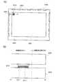
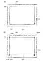
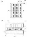
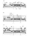
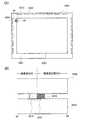
光電変換装置を液晶パネルの背面のうち画素部に配置した場合の構成について、図1(A)及び図1(B)を参照して説明する。A structure in the case where the photoelectric conversion device is arranged in the pixel portion in the back surface of the liquid crystal panel will be described with reference to FIGS.
図1(A)は、光電変換装置を液晶パネルの背面のうち画素部に配置した場合の上面図である。液晶パネル5000は、画素部5002と画素周辺部5001とに分かれている。画素部5002には複数の画素がマトリクス状に配置されている。画素周辺部5001には、信号線入力端子5003及び走査線入力端子5004が形成されている。そして、信号線が信号線入力端子5003から列方向に延在して形成され、走査線が走査線入力端子5004から延在して形成されている。こうすることで、信号線に入力されている信号と走査線に入力されている信号とによって、個々の画素を独立して制御することができる。つまり、画素部5002に画像を表示することが可能となる。FIG. 1A is a top view in the case where the photoelectric conversion device is arranged in the pixel portion of the back surface of the liquid crystal panel. The
なお、画素周辺部5001には、信号線駆動回路、走査線駆動回路、又は様々な論理回路が形成されていてもよい。画素周辺部5001には、ICチップが配置されていてもよい。Note that a signal line driver circuit, a scan line driver circuit, or various logic circuits may be formed in the pixel
光電変換装置5010は、液晶パネル5000の背面のうち画素部5002に配置されている。外部からの光(外光とも言う)は、液晶表示パネル視認側の表示画面において、一部は入射光となって液晶表示パネル内に透過し、他は反射光となって視認側に反射する。表示に有効に利用することのできる光は、液晶表示パネル内に入射した光である。もし、液晶表示パネル視認側の表示画面に光電変換装置を設ける構成であると、表示画面表面で反射してしまう光も検知してしまうことになり、正確な光の検知が困難になってしまう。本実施の形態のように液晶パネル5000とバックライト装置5020との間に、光を検知するセンサ部を有する光電変換装置5010を設ける構成であると、液晶パネル5000内を透過した光のみを正確に検知することができる。The
光電変換装置は、液晶パネルを透過した外光を検知するために、光電変換装置により光を検知する際は、液晶パネルは光を透過できる状態(白表示状態)としておく。Since the photoelectric conversion device detects external light transmitted through the liquid crystal panel, the liquid crystal panel is set in a state capable of transmitting light (white display state) when detecting light by the photoelectric conversion device.
また、光電変換装置5010が液晶表示パネルを透過した外光を検知する時に、その領域に対応するバックライト装置を消灯すれば、光電変換装置5010はバックライト装置の光を検知せずに外光の光だけを検知することができる。画素部5002で表示される画像に、光電変換装置5010が影響を与えることを防止することができる。Further, when the
図1(B)は、図1(A)に示した線A1−B1の断面図を示す。なお、図1(A)と同様なものは同じ記号を用いてその説明を省略する。すでに述べたように、光電変換装置5010は液晶パネル5000の背面のうち画素部5002に配置されている。したがって、図1(B)に示すように、光電変換装置5010は、液晶パネル5000とバックライト装置5020とに挟まれるように配置されている。なお、光電変換装置5010は、センサ部5011とセンサ部5011を駆動するための駆動部5012とを有する。そして、センサ部5011は液晶パネル5000側を向いて配置されている。駆動部5012はセンサ部5011と液晶パネル5000との間以外であれば、図1(B)のようにセンサ部5011の下に配置されていてもよいし、センサ部5011の横に配置されていてもよいし、センサ部5011を包み込むように配置されていてもよい。駆動部5012をバックライト装置側に設けることにより、バックライト装置からの液晶パネル5000と反対側から入射する光を駆動部5012によって遮断することができ、光電変換装置5010は液晶パネル5000側から入射する光をさらに正確に検知することができる。また、駆動部5012で、バックライト装置からの光よりセンサ部5011を遮光することができる場合は、センサ部で光を探知する際にバックライト装置を必ずしも消灯しなくてもよい。FIG. 1B illustrates a cross-sectional view taken along line A1-B1 illustrated in FIG. Note that components similar to those in FIG. 1A are denoted by the same reference numerals, and description thereof is omitted. As already described, the
なお、光電変換装置5010を配置する箇所は、図1(A)に限定されず、画素部5002に相当する液晶パネル5000の背面であれば様々な箇所に配置することができる。Note that the place where the
まず、光電変換装置を備えた液晶表示装置のシステムブロックの一例について、図5を参照して説明する。First, an example of a system block of a liquid crystal display device including a photoelectric conversion device will be described with reference to FIG.
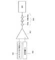
画素部1005には、信号線1011が信号線駆動回路1003から延伸して配置されている。走査線1010が走査線駆動回路1004から延伸して配置されている。そして、信号線1011と走査線1010との交差領域に、複数の画素がマトリクス状に配置されている。なお、複数の画素それぞれはスイッチング素子を有している。したがって、複数の画素それぞれに液晶分子の傾きを制御するための電圧を独立して入力することができる。このように各交差領域にスイッチング素子が設けられた構造をアクティブマトリクス型と呼ぶ。ただし、このようなアクティブマトリクス型に限定されず、パッシブマトリクス型の構成でもよい。パッシブマトリクス型は、各画素にスイッチング素子がないため、工程が簡便である。In the pixel portion 1005, the signal line 1011 is extended from the signal
光電変換装置1009は、光を検知する機能を有している。そして、検知した光に応じた信号を制御回路1002に出力する機能を有する。なお、検知した光に応じた信号を映像信号1001にフィードバックしてもよい。The
駆動回路部1008は、制御回路1002、信号線駆動回路1003及び走査線駆動回路1004を有している。制御回路1002には光電変換装置1009が出力する信号、及び映像信号1001が入力されている。制御回路1002は、光電変換装置1009が出力する信号、及び映像信号1001に応じて、信号線駆動回路1003及び走査線駆動回路1004をそれぞれ制御する。そのため、制御回路1002は、信号線駆動回路1003及び走査線駆動回路1004にそれぞれ制御信号を出力する。そして、この制御信号に応じて、信号線駆動回路1003は信号線1011にビデオ信号を出力し、走査線駆動回路1004は走査線1010に走査信号を出力する。そして、画素が有するスイッチング素子が走査信号に応じて選択され、選択された画素にビデオ信号が入力される。The
なお、制御回路1002は、光電変換装置1009が出力する信号、及び映像信号1001に応じて電源1007も制御している。電源1007は、バックライト装置1006へ電力を供給する手段を有している。制御回路1002は、光電変換装置1009が出力する信号に応じて、電源1007がバックライト装置1006へ供給する電力を調整する。例えば、光電変換装置1009が検知した光量が大きければ、それに応じて電源1007がバックライト装置1006へ供給する電力を大きくする。こうすることで、液晶表示装置の輝度が高くなるため、液晶表示装置の表示部が見づらくなることを防止することができる。一方、光電変換装置1009が検知した光量が小さければ、それに応じて電源1007がバックライト装置1006へ供給する電力を小さくする。こうすることで、必要以上に液晶表示装置の輝度を高くしなくてもよいため、液晶表示装置の消費電力を低減することができる。なお、バックライト装置1006としては、エッジライト式のバックライト装置、直下式のバックライト装置、又はフロントライトを用いてもよい。フロントライトとは、画素部の前面側に取りつけ、全体を照らす発光体及び導光体で構成された板状のライトユニットである。このようなバックライト装置により、低消費電力で、均等に画素部を照らすことができる。Note that the
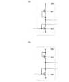
光電変換装置1009の構成の一例を図2(A)を参照して説明する。光電変換装置1009は、センサ部2001、制御部2002及びAD変換回路2003として機能する部分を有する。センサ部2001は、光を検知する機能を有している。制御部2002は、センサ部2001が光を検知するタイミングを制御する機能を有する。AD変換回路2003は、センサ部2001が検出した光に応じた電流又は電圧をアナログ値からデジタル値に変換する機能を有する。なお、光電変換装置1009の構成はこれに限定されず、様々な構成を用いることができる。An example of a structure of the
走査線駆動回路1004の構成の一例を図2(B)を参照して説明する。走査線駆動回路1004は、シフトレジスタ2011、レベルシフタ2012及びバッファ2013として機能する回路を有する。シフトレジスタ2011には制御回路1002からゲートスタートパルス(GSP)、ゲートクロック信号(GCK)等の信号が入力される。なお、走査線駆動回路1004の構成はこれに限定されず、様々な構成を用いることができる。An example of a structure of the scan
信号線駆動回路1003の構成の一例を図2(C)を参照して説明する。信号線駆動回路1003は、シフトレジスタ2021、第1のラッチ2022、第2のラッチ2023、レベルシフタ2024及びバッファ2025として機能する回路を有する。バッファ2025として機能する回路とは、弱い信号を増幅させる機能を有する回路であり、オペアンプ等を有する。シフトレジスタ2021にはスタートパルス(SSP)等の信号が入力される。第1のラッチ2022にはビデオ信号等のデータ(DATA)が入力される。第2のラッチ2023にはラッチ信号が入力される。第2のラッチ2023は第1のラッチ2022から入力される信号を一時保持することができ、ラッチ信号に応じて一斉に画素へ保持した信号を出力することができる。これを線順次駆動と呼ぶ。なお、線順次駆動ではなく、点順次駆動を行う場合は、第2のラッチ2023は不要となる。なお、信号線駆動回路1003の構成はこれに限定されず、様々な構成を用いることができる。An example of a structure of the signal
次に、光電変換装置を備えた液晶表示装置のシステムブロックの動作の一例について、図3を参照して説明する。Next, an example of operation of a system block of a liquid crystal display device including a photoelectric conversion device will be described with reference to FIG.
図3は、1画面分の画像を表示する期間に相当する1フレーム期間を示す。ただし、1フレーム期間は特に限定はしないが、画像を見る人がちらつき(フリッカー)を感じないように1/60秒以下とすることが好ましい。なお、図3のタイミングチャートは、バックライト装置(照明手段)が点灯するタイミング、光電変換装置が光を検出するタイミング、及び画素部にビデオ信号が書き込まれるタイミング(走査するタイミング)を示している。FIG. 3 shows one frame period corresponding to a period for displaying an image for one screen. However, the period of one frame is not particularly limited, but is preferably 1/60 second or less so that a person viewing the image does not feel flicker. Note that the timing chart in FIG. 3 shows the timing at which the backlight device (illuminating unit) is turned on, the timing at which the photoelectric conversion device detects light, and the timing at which a video signal is written into the pixel portion (scanning timing). .
図3のタイミングチャートでは、1フレーム期間を書き込み期間と点灯期間とに分割することができる。In the timing chart of FIG. 3, one frame period can be divided into a writing period and a lighting period.
書き込み期間での動作について説明する。書き込み期間では、各画素にビデオ信号が入力される。つまり、走査線は書き込み期間において走査され、ビデオ信号が各画素に入力される。なお、書き込み期間ではバックライト装置は非点灯状態となっている。このとき、光電変換装置は光を検知する。こうすることで、光電変換装置は、正確な外光を検知することができる。なぜなら、バックライト装置が点灯していないので、光電変換装置は外光だけを検知することができるからである。The operation in the writing period will be described. In the writing period, a video signal is input to each pixel. That is, the scanning line is scanned in the writing period, and a video signal is input to each pixel. Note that the backlight device is not lit in the writing period. At this time, the photoelectric conversion device detects light. By doing so, the photoelectric conversion device can accurately detect external light. This is because the backlight device is not lit, so that the photoelectric conversion device can detect only external light.
点灯期間での動作について説明する。点灯期間では、各画素へのビデオ信号の書き込み動作は行われない。したがって、各画素は書き込み期間において入力されたビデオ信号をそれぞれ保持している。そして、各画素がそれぞれ有する液晶素子は、ビデオ信号に応じた透過率となっている。このとき、バックライト装置が点灯することによって、ビデオ信号に応じた画像を表示することができる。The operation during the lighting period will be described. In the lighting period, the video signal writing operation to each pixel is not performed. Therefore, each pixel holds a video signal input during the writing period. And the liquid crystal element which each pixel has has the transmittance | permeability according to a video signal. At this time, when the backlight device is turned on, an image corresponding to the video signal can be displayed.
図3とは別の光電変換装置を備えた液晶表示装置のシステムブロックの動作の一例について、図4(A)及び図4(B)を参照して説明する。An example of operation of a system block of a liquid crystal display device including a photoelectric conversion device different from that in FIG. 3 will be described with reference to FIGS.
図4(A)は、1画面分の画像を表示する期間に相当する1フレーム期間を示す。ただし、1フレーム期間は特に限定はしないが、画像を見る人がちらつき(フリッカー)を感じないように1/60秒以下とすることが好ましい。FIG. 4A shows one frame period corresponding to a period for displaying an image for one screen. However, the period of one frame is not particularly limited, but is preferably 1/60 second or less so that a person viewing the image does not feel flicker.
動作について説明する。まず、書き込み期間Taにおいて、1行目から順に走査線に走査信号が入力され、画素が選択される。そして、画素が選択されているときに、信号線から画素へビデオ信号が入力される。そして、画素にビデオ信号が書き込まれると、画素は再び信号が入力されるまでその信号を保持する。この書き込まれたビデオ信号によって表示期間Tsにおける各画素の階調が制御される。なお、バックライト装置消灯期間Tcにおいて、走査線を走査する動作に合わせてバックライト装置が消灯する。バックライト装置消灯期間Tcは書き込み期間Taよりも長い。このバックライト装置消灯期間Tcにおいて、光電変換装置が配置されている付近のバックライト装置が消灯したときに、光電変換装置は光を検知する。こうすることで、光電変換装置は、正確な外光を検知することができる。なぜなら、バックライト装置が点灯していないので、光電変換装置は外光だけを検知することができるからである。The operation will be described. First, in the writing period Ta, scanning signals are input to the scanning lines in order from the first row, and pixels are selected. When a pixel is selected, a video signal is input from the signal line to the pixel. When a video signal is written to the pixel, the pixel holds the signal until the signal is input again. The gradation of each pixel in the display period Ts is controlled by the written video signal. In the backlight device extinguishing period Tc, the backlight device is extinguished in accordance with the scanning line scanning operation. The backlight device extinguishing period Tc is longer than the writing period Ta. In the backlight device extinction period Tc, when the backlight device in the vicinity where the photoelectric conversion device is disposed is extinguished, the photoelectric conversion device detects light. By doing so, the photoelectric conversion device can accurately detect external light. This is because the backlight device is not lit, so that the photoelectric conversion device can detect only external light.
ここで、図4(B)を参照して、i行目の画素行に着目して説明する。まず、書き込み期間Taにおいて1行目から順に走査線に走査信号が入力される。そして、書き込み期間Taのうち期間Tb(i)において、i行目の画素が選択される。i行目の画素が選択されているときに、信号線からi行目の画素にビデオ信号が入力される。そして、i行目の画素にビデオ信号が書き込まれると、i行目の画素は再び信号が入力されるまでその信号を保持する。この書き込まれたビデオ信号によって表示期間Ts1におけるi行目の画素の階調が制御される。なお、期間Tb(i)、及びその前後の期間では、バックライト装置が非点灯状態となる。このバックライト装置が消灯している期間が期間Td(i)である。そして、i行目付近に光電変換装置が配置されている場合は、期間Td(i)において光電変換装置は光を検知する。こうすることで、光電変換装置は、正確な外光を検知することができる。なぜなら、バックライト装置が点灯していないので、光電変換装置は外光だけを検知することができるからである。Here, the i-th pixel row will be described with reference to FIG. First, scanning signals are input to the scanning lines in order from the first row in the writing period Ta. Then, in the writing period Ta, the pixel in the i-th row is selected in the period Tb (i). When the pixel in the i-th row is selected, a video signal is input from the signal line to the pixel in the i-th row. When a video signal is written to the i-th row pixel, the i-th row pixel holds the signal until the signal is input again. The gradation of the pixel in the i-th row in the display period Ts1 is controlled by the written video signal. Note that the backlight device is not lit in the period Tb (i) and the periods before and after the period Tb (i). A period during which the backlight device is turned off is a period Td (i). When the photoelectric conversion device is arranged near the i-th row, the photoelectric conversion device detects light in the period Td (i). By doing so, the photoelectric conversion device can accurately detect external light. This is because the backlight device is not lit, so that the photoelectric conversion device can detect only external light.
本発明を適用した本実施の形態において、光電変換装置を液晶表示パネルとバックライト装置との間に設けることによって、液晶表示装置を大型化することなく、表示に影響を与える外部から液晶表示パネルに入射する光のみを光センサで効率よく検知することができる。よって、最適な表示輝度に液晶表示装置の表示部を調整することができる。In this embodiment to which the present invention is applied, by providing a photoelectric conversion device between a liquid crystal display panel and a backlight device, the liquid crystal display panel from the outside that affects the display without increasing the size of the liquid crystal display device Only the light incident on the light can be efficiently detected by the optical sensor. Therefore, the display unit of the liquid crystal display device can be adjusted to the optimum display luminance.
従って、本発明により、より小型で高精度な輝度調整機能を有する液晶表示装置を提供することができる。本発明の液晶表示装置は、輝度調整機能により、高画質化及び低消費電力化を達成することができる。Therefore, according to the present invention, it is possible to provide a liquid crystal display device having a smaller and more accurate brightness adjustment function. The liquid crystal display device of the present invention can achieve high image quality and low power consumption by the brightness adjustment function.
なお、本実施の形態において、様々な図を用いて述べてきたが、各々の図で述べた内容(一部でもよい)は、別の図で述べた内容(一部でもよい)に対して、適用、組み合わせ、又は置き換えなどを自由に行うことができる。さらに、これまでに述べた図において、各々の部分に関して、別の部分を組み合わせることにより、さらに多くの図を構成させることができる。Note that in this embodiment mode, description has been made using various drawings. However, the contents (or part of the contents) described in each figure may be different from the contents (or part of the contents) described in another figure. , Application, combination, or replacement can be performed freely. Further, in the drawings described so far, more parts can be formed by combining each part with another part.
同様に、本実施の形態の各々の図で述べた内容(一部でもよい)は、別の実施の形態の図で述べた内容(一部でもよい)対して、適用、組み合わせ、又は置き換えなどを自由に行うことができる。さらに、本実施の形態の図において、各々の部分に関して、別の実施の形態の部分を組み合わせることにより、さらに多くの図を構成させることができる。Similarly, the contents (may be a part) described in each drawing of this embodiment are applied, combined, or replaced with the contents (may be a part) described in the figure of another embodiment. Can be done freely. Further, in the drawings of this embodiment mode, more drawings can be formed by combining each portion with a portion of another embodiment.
なお、本実施の形態は、他の実施の形態で述べた内容(一部でもよい)を、具現化した場合の一例、少し変形した場合の一例、一部を変更した場合の一例、改良した場合の一例、詳細に述べた場合の一例、応用した場合の一例、関連がある部分についての一例などを示している。したがって、他の実施の形態で述べた内容は、本実施の形態への適用、組み合わせ、又は置き換えを自由に行うことができる。Note that the present embodiment is an example in which the contents (may be part) described in other embodiments are embodied, an example in which the content is slightly modified, an example in which a part is changed, and an improvement. An example of a case, an example of a case where it is described in detail, an example of a case where it is applied, an example of a related part, and the like are shown. Therefore, the contents described in other embodiments can be freely applied to, combined with, or replaced with this embodiment.
(実施の形態2)
本実施の形態では、実施の形態1とは別の光電変換装置を液晶パネルの背面に配置した場合の構成について説明する。なお、本実施の形態で説明する液晶パネルの構成に限定はなく、様々な構成を用いることができる。なお、本実施の形態で説明する光電変換装置の構成に限定はなく、様々な構成を用いることができる。なお、本実施の形態で説明するバックライト装置の構成に限定はなく、様々な構成を用いることができる。(Embodiment 2)
In this embodiment, a structure in the case where a photoelectric conversion device different from that in
光電変換装置を液晶パネルの背面のうち画素部に配置した場合の構成について、図32(A)及び図32(B)を参照して説明する。なお、実施の形態1で説明した図1(A)及び図1(B)と同様なものには同じ符号を用いてその説明を省略する。A structure in the case where the photoelectric conversion device is arranged in the pixel portion on the back surface of the liquid crystal panel will be described with reference to FIGS. 32A and 32B. Note that components similar to those in FIGS. 1A and 1B described in
図32(A)は、光電変換装置を液晶パネルの背面のうち画素部に配置し、その一部を液晶パネルの背面のうち画素周辺部に配置した場合の上面図である。なお、光電変換装置5010のセンサ部は、液晶パネル5000の背面のうち画素部5002に配置されている。一方、光電変換装置5010の駆動部は、液晶パネル5000の背面のうち画素部5002に配置されていてもよいし、液晶パネル5000の背面のうち画素周辺部5001に配置されていてもよい。こうすることで、液晶パネル5000の画素部5002を透過する光量の低減を抑えることができる。FIG. 32A is a top view in the case where the photoelectric conversion device is arranged in the pixel portion of the back surface of the liquid crystal panel and a part thereof is arranged in the pixel peripheral portion of the back surface of the liquid crystal panel. Note that the sensor portion of the
図32(B)は、図32(A)に示した線A8−B8の断面図を示す。なお、図32(A)と同様なものは同じ記号を用いてその説明を省略する。すでに述べたように、光電変換装置5010は、液晶パネル5000の背面のうち画素部5002に配置し、その一部が液晶パネルの背面のうち画素周辺部5001に配置されている。したがって、図32(B)に示すように、光電変換装置5010は、液晶パネル5000とバックライト装置5020とに挟まれるように配置されている。なお、光電変換装置5010は、センサ部5011とセンサ部5011を駆動するための駆動部5012とを有する。そして、センサ部5011は、バックライト装置5020と液晶パネル5000の画素部5002との間に配置されている。駆動部5012は、バックライト装置5020と液晶パネル5000の画素周辺部5001との間に配置されている。こうすることで、液晶パネル5000の画素部5002を透過する光量の低減を抑えることができる。FIG. 32B is a cross-sectional view taken along line A8-B8 shown in FIG. Note that components similar to those in FIG. 32A are denoted by the same reference numerals, and description thereof is omitted. As already described, the
なお、光電変換装置5010を配置する箇所は、図32(A)に限定されず、画素部5002に相当する液晶パネル5000の背面であれば様々な箇所に配置することができる。例えば、図6(A)に示すように、光電変換装置5010を図32(A)とは異なる箇所に配置してもよい。あるいは、図6(B)に示すように、複数の光電変換装置(光電変換装置5010a、光電変換装置5010b、光電変換装置5010c及び光電変換装置5010d)が配置されていてもよい。こうすることで、それぞれの光電変換装置で光を検知して、それらの情報を平均して液晶表示装置の周辺の明るさを求めることができる。したがって、正確な液晶表示装置の周辺の明るさを求めることができる。Note that the place where the
図1(A)、図1(B)、図6(A)、図6(B)、図32(A)及び図32(B)よりも詳細な、光電変換装置を液晶パネルの背面のうち画素部に配置した場合の構成について、図7(A)及び図7(B)を参照して説明する。1A, FIG. 1B, FIG. 6A, FIG. 6B, FIG. 32A, and FIG. 32B, the photoelectric conversion device is more detailed than the back side of the liquid crystal panel. A structure in the case of being arranged in the pixel portion will be described with reference to FIGS. 7A and 7B.
図7(A)は、光電変換装置を液晶パネルの背面のうち画素周辺部に配置した場合の上面図である。なお、図7(A)は、画素部周辺部を拡大して示した領域7000の上面図である。領域7000は、遮光領域7001と透光領域7002とに分けることができる。遮光領域7001とは光が透過しない領域のことをいう。透光領域7002とは光が透過する領域のことをいう。図7(A)では、遮光領域7001には配線が形成され、透光領域7002には何も形成されていない。なお、遮光領域7001には、配線の他に、ブラックマトリクス、トランジスタ、反射電極、又は様々な素子が形成されていてもよい。あるいは、ICチップなどが配置されていてもよい。なお、透光領域7002には、透明性を有する材料で形成される膜、透光性を有する薄い膜、シリコンなどが形成されていてもよい。FIG. 7A is a top view in the case where the photoelectric conversion device is arranged in the pixel peripheral portion of the back surface of the liquid crystal panel. Note that FIG. 7A is a top view of a
光電変換装置7010は、液晶パネルの背面のうち遮光領域7001に配置されている。そして、光電変換装置7010の一部が液晶パネルの背面のうち透光領域7002に配置されている。The
図7(B)は、図7(A)に示したA2−B2の断面図を示す。なお、図7(A)と同様なものは同じ記号を用いてその説明を省略する。すでに述べたように、光電変換装置7010は液晶パネルの背面のうち画素周辺部に配置されている。したがって、図7(B)に示すように、光電変換装置7010は、液晶パネル7030とバックライト装置7020とに挟まれるように配置されている。なお、光電変換装置7010は、センサ部7011とセンサ部7011を駆動するための駆動部7012とに分けることができる。そして、センサ部7011は、液晶パネル7030のうち画素周辺部の透光領域7002に配置されている。駆動部7012の大部分は、液晶パネル7030の背面のうち画素周辺部の遮光領域7001に配置されている。こうすることで、透光領域7002が小さい領域(複数の配線が形成されている場所など)に、光電変換装置7010を配置することができる。この理由について説明する。外光が入射する場所にセンサ部7011が配置されていれば、光電変換装置7010は外光を検知することができる。駆動部7012は、外光が入射する場所に配置する必要はない。したがって、図7(A)に示すように、センサ部7011が透光領域7002に配置されていれば、駆動部7012が遮光領域7001に配置されていても、光電変換装置7010は外光を検知することができる。FIG. 7B is a cross-sectional view taken along the line A2-B2 illustrated in FIG. Note that components similar to those in FIG. 7A are denoted by the same symbols, and description thereof is omitted. As already described, the
なお、光電変換装置7010が配置される場所はこれに限定されず、様々な場所に配置することができる。例えば、トランジスタが配置されている箇所、ブラックマトリクスが形成されている箇所などに、光電変換装置7010を配置することができる。Note that the place where the
次に、図7(A)及び図7(B)とは別の光電変換装置を液晶パネルの背面のうち画素部に配置した場合の構成について、図8(A)及び図8(B)を参照して説明する。Next, FIGS. 8A and 8B illustrate a structure in the case where a photoelectric conversion device different from those in FIGS. 7A and 7B is provided in the pixel portion of the back surface of the liquid crystal panel. The description will be given with reference.
図8(A)は、光電変換装置を液晶パネルの背面のうち画素部に配置した場合の上面図である。なお、図8(A)は、画素部を拡大して示し、画素8001、画素8002及び画素8003を示している。なお、図示はしないが、画素部には他にも複数の画素が配置されている。画素8001、画素8002及び画素8003は、半透過型の構造である。したがって、画素8001は反射領域8004と透光領域8007とに分けられている。同様に、画素8002は反射領域8005と透光領域8008、画素8003は反射領域8006と透光領域8009とにそれぞれ分けられている。反射領域8004、反射領域8005及び反射領域8006はそれぞれ、光が入射するとその光を反射する機能を有する。透光領域8007、透光領域8008及び透光領域8009はそれぞれ、バックライト装置の光を透過する機能を有している。FIG. 8A is a top view in the case where the photoelectric conversion device is arranged in the pixel portion in the back surface of the liquid crystal panel. Note that FIG. 8A illustrates an enlarged pixel portion, which illustrates a
光電変換装置8010は、液晶パネルの背面のうち反射領域(反射領域8004、反射領域8005及び反射領域8006)にそれぞれ配置されている。そして、光電変換装置8010の一部が液晶パネルの背面のうち透光領域(透光領域8007、透光領域8008及び透光領域8009)にそれぞれ配置されている。こうすることで、画素部に光電変換装置を配置しても、画素の光を透過できる面積の減少を少なくすることができる。The
図8(B)は、図8(A)に示したA3−B3の断面図を示す。なお、図8(A)と同様なものは同じ記号を用いてその説明を省略する。すでに述べたように、光電変換装置8010は液晶パネルの背面のうち画素部に配置されている。したがって、図8(B)に示すように、光電変換装置8010は、液晶パネル8030とバックライト装置8020とに挟まれるように配置されている。なお、光電変換装置8010は、センサ部8011とセンサ部8011を駆動するための駆動部8012とに分けることができる。そして、センサ部8011は、液晶パネル8030のうち画素部の透光領域8007に配置されている。駆動部8012の大部分は、液晶パネル8030の背面のうち反射領域8004に配置されている。こうすることで、光電変換装置を液晶パネルの背面のうち画素部に配置しても、画素の輝度の低下を抑えることができる。FIG. 8B illustrates a cross-sectional view of A3-B3 illustrated in FIG. Note that components similar to those in FIG. 8A are denoted by the same reference numerals, and description thereof is omitted. As already described, the
なお、光電変換装置8010の駆動部8012に反射性の材料を形成することで、画素に反射電極を形成するための工程を削減することができる。あるいは、駆動部8012の材料の一部に反射性を持たせることで、画素に反射電極を形成するための工程を削減することができる。Note that by forming a reflective material in the
なお、図8(A)及び図8(B)では、3つの画素の領域に1つの光電変換装置を配置した場合について説明したがこれに限定されず、様々な構成を用いることができる。例えば、1画素に1つの光電変換装置を配置してもよい。4画素以上の領域に1つの光電変換装置を配置してもよい。Note that FIGS. 8A and 8B illustrate the case where one photoelectric conversion device is provided in a region of three pixels; however, the present invention is not limited to this, and various structures can be used. For example, one photoelectric conversion device may be arranged for one pixel. One photoelectric conversion device may be arranged in an area of 4 pixels or more.
なお、全ての画素の領域に光電変換装置を配置してもよい。あるいは、特定の画素の領域だけに光電変換装置を配置してもよい。Note that photoelectric conversion devices may be arranged in all pixel regions. Or you may arrange | position a photoelectric conversion apparatus only to the area | region of a specific pixel.
なお、図8(A)及び図8(B)では、光電変換装置が画素部に配置されている場合について説明したが、表示に寄与しない画素が形成される領域に光電変換装置を配置してもよい。Note that FIGS. 8A and 8B illustrate the case where the photoelectric conversion device is provided in the pixel portion; however, the photoelectric conversion device is provided in a region where a pixel that does not contribute to display is formed. Also good.
図8(A)及び図8(B)とは別の光電変換装置を液晶パネルの背面のうち画素部に配置した場合の構成について図9(A)及び図9(B)素を参照して説明する。With reference to FIGS. 9A and 9B, a structure in the case where a photoelectric conversion device different from those in FIGS. 8A and 8B is arranged in the pixel portion on the back surface of the liquid crystal panel is described. explain.
図9(A)は、光電変換装置を液晶パネルの背面のうち画素部に配置した場合の上面図である。なお、図9(A)は、画素部を拡大して示し、画素9001、画素9002及び画素9003を示している。なお、図示はしないが、画素部には複数の画素が配置されている。画素9001、画素9002及び画素9003は、半透過型の構造である。したがって、画素9001は反射領域9004と透光領域9007とに分けられている。同様に、画素9002は反射領域9005と透光領域9008、画素9003は反射領域9006と透光領域9009とにそれぞれ分けられている。反射領域9004、反射領域9005及び反射領域9006はそれぞれ、光が入射するとその光を反射する機能を有する。透光領域9007、透光領域9008及び透光領域9009はそれぞれ、バックライト装置の光を透過する機能を有している。FIG. 9A is a top view in the case where the photoelectric conversion device is arranged in the pixel portion in the back surface of the liquid crystal panel. Note that FIG. 9A illustrates an enlarged pixel portion, which illustrates a
光電変換装置9010は、液晶パネルの背面のうち反射領域9004に配置されている。そして、光電変換装置9010の一部が液晶パネルの背面のうち透光領域9007に配置されている。同様に、光電変換装置9050は、液晶パネルの背面のうち反射領域9005に配置されている。そして、光電変換装置9050の一部が液晶パネルの背面のうち透光領域9008に配置されている。同様に、光電変換装置9040は、液晶パネルの背面のうち反射領域9006に配置されている。そして、光電変換装置9040の一部が液晶パネルの背面のうち透光領域9009に配置されている。こうすることで、画素部に光電変換装置を配置しても、画素の光を透過できる面積の減少を少なくすることができる。The
図9(B)は、図9(A)に示したA4−B4の断面図を示す。なお、図9(A)と同様なものは同じ記号を用いてその説明を省略する。すでに述べたように、光電変換装置9010は液晶パネルの背面のうち画素部に配置されている。したがって、図9(B)に示すように、光電変換装置9010は、液晶パネル9030とバックライト装置9020とに挟まれるように配置されている。なお、光電変換装置9010は、センサ部9011とセンサ部9011を駆動するための駆動部9012とに分けることができる。なお、光電変換装置9040及び光電変換装置9050もそれぞれ、センサ部と駆動部とに分けることができる。そして、センサ部9011は、液晶パネル9030のうち画素部の透光領域9007に配置されている。駆動部9012の大部分は、液晶パネル9030の背面のうち反射領域9004に配置されている。なお、光電変換装置9050及び光電変換装置9040も光電変換装置9010と同様にそれぞれ、画素9002と画素9003とに配置されている。こうすることで、光電変換装置を液晶パネルの背面のうち画素部に配置しても、画素の輝度の低下を抑えることができる。なお、光電変換装置のセンサ部(センサ部9011)はカラーフィルタ9031を介した外光を検知する。したがって、光電変換装置は特定の色要素の光だけを検知することができる。FIG. 9B shows a cross-sectional view of A4-B4 shown in FIG. Note that components similar to those in FIG. 9A are denoted by the same reference numerals, and description thereof is omitted. As already described, the
なお、画素9001、画素9002及び画素9003にそれぞれ、R、G、Bのカラーフィルタが配置されている場合、光電変換装置9010、光電変換装置9050及び光電変換装置9040はそれぞれ、Rの色要素の外光、Gの色要素の外光、Bの色要素の外光だけを検知することができる。Note that in the case where R, G, and B color filters are provided for the
なお、光電変換装置9010、光電変換装置9050及び光電変換装置9040のそれぞれの駆動部に反射性の材料を形成することで、画素に反射電極を形成するための工程を削減することができる。あるいは、光電変換装置9010、光電変換装置9050及び光電変換装置9040のそれぞれの駆動部の材料の一部に反射性を持たせることで、画素に反射電極を形成するための工程を削減することができる。Note that by forming a reflective material in each driving portion of the
なお、画素部に形成されている画素の全てに、それぞれ光電変換装置を配置してもよい。あるいは、特定の画素だけに光電変換装置を配置してもよい。Note that a photoelectric conversion device may be provided for each of the pixels formed in the pixel portion. Or you may arrange | position a photoelectric conversion apparatus only to a specific pixel.
なお、図9(A)及び図9(B)では、光電変換装置が画素部に配置されている場合について説明したが、表示に寄与しない画素が配置されている領域に光電変換装置を配置してもよい。Note that FIGS. 9A and 9B illustrate the case where the photoelectric conversion device is provided in the pixel portion; however, the photoelectric conversion device is provided in a region where pixels that do not contribute to display are provided. May be.
本発明を適用した本実施の形態において、光電変換装置を液晶パネルとバックライト装置との間に設けることによって、液晶表示装置を大型化することなく、表示に影響を与える外部から液晶パネルに入射する光のみを光センサで効率よく検知することができる。よって、最適な表示輝度に液晶表示装置の表示部を調整することができる。In this embodiment to which the present invention is applied, the photoelectric conversion device is provided between the liquid crystal panel and the backlight device, so that the liquid crystal display device is incident on the liquid crystal panel from the outside which affects the display without increasing the size. Only the light to be detected can be efficiently detected by the optical sensor. Therefore, the display unit of the liquid crystal display device can be adjusted to the optimum display luminance.
従って、本発明により、より小型で高精度な輝度調整機能を有する液晶表示装置を提供することができる。本発明の液晶表示装置は、輝度調整機能により、高画質化及び低消費電力化を達成することができる。Therefore, according to the present invention, it is possible to provide a liquid crystal display device having a smaller and more accurate brightness adjustment function. The liquid crystal display device of the present invention can achieve high image quality and low power consumption by the brightness adjustment function.
なお、本実施の形態において、様々な図を用いて述べてきたが、各々の図で述べた内容(一部でもよい)は、別の図で述べた内容(一部でもよい)に対して、適用、組み合わせ、又は置き換えなどを自由に行うことができる。さらに、これまでに述べた図において、各々の部分に関して、別の部分を組み合わせることにより、さらに多くの図を構成させることができる。Note that in this embodiment mode, description has been made using various drawings. However, the contents (or part of the contents) described in each figure may be different from the contents (or part of the contents) described in another figure. , Application, combination, or replacement can be performed freely. Further, in the drawings described so far, more parts can be formed by combining each part with another part.
同様に、本実施の形態の各々の図で述べた内容(一部でもよい)は、別の実施の形態の図で述べた内容(一部でもよい)対して、適用、組み合わせ、又は置き換えなどを自由に行うことができる。さらに、本実施の形態の図において、各々の部分に関して、別の実施の形態の部分を組み合わせることにより、さらに多くの図を構成させることができる。Similarly, the contents (may be a part) described in each drawing of this embodiment are applied, combined, or replaced with the contents (may be a part) described in the figure of another embodiment. Can be done freely. Further, in the drawings of this embodiment mode, more drawings can be formed by combining each portion with a portion of another embodiment.
なお、本実施の形態は、他の実施の形態で述べた内容(一部でもよい)を、具現化した場合の一例、少し変形した場合の一例、一部を変更した場合の一例、改良した場合の一例、詳細に述べた場合の一例、応用した場合の一例、関連がある部分についての一例などを示している。したがって、他の実施の形態で述べた内容は、本実施の形態への適用、組み合わせ、又は置き換えを自由に行うことができる。Note that the present embodiment is an example in which the contents (may be part) described in other embodiments are embodied, an example in which the content is slightly modified, an example in which a part is changed, and an improvement. An example of a case, an example of a case where it is described in detail, an example of a case where it is applied, an example of a related part, and the like are shown. Therefore, the contents described in other embodiments can be freely applied to, combined with, or replaced with this embodiment.
(実施の形態3)
本実施の形態では、光電変換装置をバックライト装置に配置した場合の構成について説明する。なお、本実施の形態で説明する液晶パネルの構成に限定はなく、様々な構成を用いることができる。なお、本実施の形態で説明する光電変換装置の構成に限定はなく、様々な構成を用いることができる。なお、本実施の形態で説明するバックライト装置の構成に限定はなく、様々な構成を用いることができる。(Embodiment 3)
In this embodiment, a structure in the case where a photoelectric conversion device is provided in a backlight device will be described. Note that there is no limitation on the structure of the liquid crystal panel described in this embodiment, and a variety of structures can be used. Note that there is no limitation on the structure of the photoelectric conversion device described in this embodiment, and various structures can be used. Note that there is no limitation on the structure of the backlight device described in this embodiment, and various structures can be used.
光電変換装置をバックライト装置に配置した場合の構成について、図10(A)及び図10(B)を参照して説明する。A structure in the case where the photoelectric conversion device is provided in a backlight device is described with reference to FIGS.
図10(A)は、光電変換装置を直下式のバックライト装置に配置した場合の上面図である。バックライト装置10000は、筐体10002上に複数の光源10001及び複数の光電変換装置10010が配置されている。なお、導光板、反射板、拡散板、ランプリフレクターなどを省略して図示する。なお、光源10001としては発光ダイオードを用いた場合の構成について説明する。光源10001と光電変換装置10010とが同じ筐体10002上に配置されていることによって、光電変換装置10010を配置するためのスペースの増加を抑えることができる。光電変換装置10010は液晶パネルの表示部を透過した光を検知することができるため、表示部周辺の明るさを検知することができる。FIG. 10A is a top view when the photoelectric conversion device is arranged in a direct-type backlight device. In the
なお、光源10001は発光ダイオードに限定されず、様々な構成を用いることができる。例えば、光源10001として、冷陰極管、熱陰極管、無機EL又は有機ELなどを用いることができる。Note that the
図10(B)は、図10(A)に示したA5−B5の断面図を示す。なお、図10(A)と同様なものは同じ記号を用いてその説明を省略する。すでに述べたように、光電変換装置10010は光源10001が配置されている筐体10002に配置されている。なお、光電変換装置10010は、センサ部10011とセンサ部10011を駆動するための駆動部10012とに分けることができる。そして、センサ部10011は上から入射する光を検知できるように配置されている。駆動部10012はセンサ部10011の下側に配置されている。こうすることによって、光電変換装置10010の配置面積を低減することができる。なお、駆動部10012は、センサ部10011が検知する光を遮らないところであれば、センサ部10011の下側に限定されず、様々なところに配置することができる。FIG. 10B illustrates a cross-sectional view of A5-B5 illustrated in FIG. Note that components similar to those in FIG. 10A are denoted by the same reference numerals, and description thereof is omitted. As already described, the
なお、光源10001及び光電変換装置10010が配置された筐体10002の上側には光学シート1113が配置されている。光学シート1113は、導光板、反射板、拡散板などから構成されている。例えば、光源10001が消灯しているときには、光電変換装置10010は、光学シート1113に拡散された外光を検知する。一方、光源10001が点灯しているときには、光電変換装置10010は、光源10001の光を検知する。したがって、図10に示した液晶表示装置は、外光の明るさ、及びバックライト装置の明るさを検知することができる。Note that an
図10(A)及び図10(B)とは別の、光電変換装置をバックライト装置に配置した場合の構成について、図11(A)及び図11(B)を参照して説明する。なお、図10(A)及び図10(B)と図11(A)及び図11(B)との違いは、光源として冷陰極管を用いたところである。A structure in which a photoelectric conversion device is provided in a backlight device, which is different from FIGS. 10A and 10B, will be described with reference to FIGS. 11A and 11B. The difference between FIGS. 10A and 10B and FIGS. 11A and 11B is that a cold cathode tube is used as the light source.
図11(A)は、光電変換装置を直下式のバックライト装置に配置した場合の上面図である。バックライト装置1100は、筐体1102上に複数の光源1101及び複数の光電変換装置1110が配置されている。なお、導光板、反射板、拡散板、ランプリフレクターなどを省略して図示する。なお、光源1101としては冷陰極管を用いた場合の構成について説明する。光源1101と光電変換装置1110とが同じ筐体1102上に配置されていることによって、光電変換装置1110を配置するためのスペースの増加を抑えることができる。光電変換装置1110は液晶パネルの表示部を透過した光を検知することができるため、表示部周辺の明るさを検知することができる。FIG. 11A is a top view in the case where the photoelectric conversion device is arranged in a direct backlight device. In the
なお、光源1101は冷陰極管に限定されず、様々な構成を用いることができる。例えば、光源1101として、熱陰極管、発光ダイオード、無機EL又は有機ELなどを用いることができる。The
図11(B)は、図11(A)に示したA6−B6の断面図を示す。なお、図11(A)と同様なものは同じ記号を用いてその説明を省略する。すでに述べたように、光電変換装置1110は光源1101が配置されている筐体1102に配置されている。なお、光電変換装置1110は、センサ部1111とセンサ部1111を駆動するための駆動部1112とに分けることができる。そして、センサ部1111は上から入射する光を検知できるように配置されている。駆動部1112はセンサ部1111の下側に配置されている。こうすることによって、光電変換装置1110の配置面積を低減することができる。なお、駆動部1112は、センサ部1111が検知する光を遮らないところであれば、センサ部1111の下側に限定されず、様々なところに配置することができる。FIG. 11B illustrates a cross-sectional view of A6-B6 illustrated in FIG. Note that components similar to those in FIG. 11A are denoted by the same reference numerals, and description thereof is omitted. As already described, the
なお、光源1101及び光電変換装置1110が配置された筐体1102の上側には光学シート1113が配置されている。光学シート1113は、導光板、反射板、拡散板などから構成されている。例えば、光源1101が消灯しているときには、光電変換装置1110は、光学シート1113に拡散された外光を検知する。一方、光源1101が点灯しているときには、光電変換装置1110は、光源1101の光を検知する。したがって、図11に示した液晶表示装置は、外光の明るさ、及びバックライト装置の明るさを検知することができる。Note that an
図10(A)、図10(B)、図11(A)及び図11(B)とは別の、光電変換装置をバックライト装置に配置した場合の構成について、図12(A)及び図12(B)を参照して説明する。FIGS. 12A and 12B illustrate a configuration in which a photoelectric conversion device is provided in a backlight device, which is different from FIGS. 10A, 10B, 11A, and 11B. This will be described with reference to FIG.
図12(A)は、光電変換装置をバックライト装置の光学シート上に配置した場合の上面図である。なお、図12(A)では、光源などは省略して説明する。光学シート1200は、導光板、反射板、拡散板などから構成されている。なお、光学シート1200は、画素周辺部対応領域1201と画素部対応領域1202とに分けることができる。光電変換装置1210は画素周辺部対応領域1201に配置されている。なお、画素周辺部対応領域1201とは、液晶パネルの画素周辺部の下側の領域である。画素部対応領域1202とは、液晶パネルの画素部の下側の領域である。FIG. 12A is a top view in the case where the photoelectric conversion device is arranged over the optical sheet of the backlight device. Note that in FIG. 12A, a light source and the like are omitted. The
なお、図12(A)に用いることができるバックライト装置は、様々な構成を用いることができる。例えば、図12(A)に用いることができるバックライト装置としては、直下式バックライト装置又はエッジライト式バックライト装置を用いることができる。Note that a variety of structures can be used for the backlight device which can be used in FIG. For example, as a backlight device that can be used in FIG. 12A, a direct backlight device or an edge light backlight device can be used.
なお、光電変換装置1210が配置されている場所は図12(A)に限定されず、様々な場所に配置することができる。なお、光電変換装置1210が配置されている数は、図12(A)に限定されず、2つ以上配置されていてもよい。Note that the place where the
図12(B)は、図12(A)に示したA7−B7の断面図を示す。なお、図12(A)と同様なものは同じ記号を用いてその説明を省略する。すでに述べたように、光電変換装置1210は光学シート1200上に配置されている。なお、光電変換装置1210は、センサ部1211とセンサ部1211を駆動するための駆動部1212とに分けることができる。そして、センサ部1211は光学シート1200に接して配置されている。駆動部1212はセンサ部1211の上側に配置されている。こうすることで、光電変換装置1210は光学シート1200の光を検知することができる。これについて具体的に説明する。光学シート1200の光は、バックライト装置が消灯状態のときは、外光の光が拡散したものである。つまり、外光が光学シート1200を介して光電変換装置1210に検知される。したがって、画素周辺部対応領域1201に外光が入射する必要は無く、液晶パネルの画素周辺部には様々なものを配置又は形成することができる。なお、バックライト装置が発光しているときは、光電変換装置1210は光学シート1200を介してバックライト装置の輝度を検知することができる。FIG. 12B is a cross-sectional view taken along line A7-B7 shown in FIG. Note that components similar to those in FIG. 12A are denoted by the same reference numerals, and description thereof is omitted. As already described, the
なお、本実施の形態において、複数の光電変換装置をバックライト装置に配置してもよいとした。これらの複数の光電変換装置は、配置する箇所、検知する光量、又は検知する色要素などによって、異なる構成又は異なる形状であってもよい。Note that in this embodiment, a plurality of photoelectric conversion devices may be provided in the backlight device. The plurality of photoelectric conversion devices may have different configurations or different shapes depending on an arrangement location, a light amount to be detected, a color element to be detected, or the like.
なお、光電変換装置がバックライト装置に設けられているため、液晶表示装置を小型にすることができる。また、光電変換装置は光源の光を検知することで、バックライト装置の劣化を補正することができる。表示に影響を与える液晶表示パネルに入射した外部からの光をセンサ部で探知し、その情報をバックライト装置へフィードバックすることで、バックライト装置の光の強度の制御を行うことができる。従って表示部の表示輝度のばらつきを防ぐことができ、高画質な表示を行うことができる。また、外光を効率よく使用することができるため、過剰なバックライト装置の駆動を防ぐことができ、液晶表示装置を高信頼性及び低消費電力とすることが可能となる。Note that since the photoelectric conversion device is provided in the backlight device, the liquid crystal display device can be downsized. In addition, the photoelectric conversion device can correct deterioration of the backlight device by detecting the light of the light source. The light intensity of the backlight device can be controlled by detecting external light incident on the liquid crystal display panel that affects the display by the sensor unit and feeding back the information to the backlight device. Therefore, variation in display luminance of the display portion can be prevented, and high-quality display can be performed. In addition, since external light can be used efficiently, excessive driving of the backlight device can be prevented, and the liquid crystal display device can have high reliability and low power consumption.
なお、本実施の形態において、様々な図を用いて述べてきたが、各々の図で述べた内容(一部でもよい)は、別の図で述べた内容(一部でもよい)に対して、適用、組み合わせ、又は置き換えなどを自由に行うことができる。さらに、これまでに述べた図において、各々の部分に関して、別の部分を組み合わせることにより、さらに多くの図を構成させることができる。Note that in this embodiment mode, description has been made using various drawings. However, the contents (or part of the contents) described in each figure may be different from the contents (or part of the contents) described in another figure. , Application, combination, or replacement can be performed freely. Further, in the drawings described so far, more parts can be formed by combining each part with another part.
同様に、本実施の形態の各々の図で述べた内容(一部でもよい)は、別の実施の形態の図で述べた内容(一部でもよい)対して、適用、組み合わせ、又は置き換えなどを自由に行うことができる。さらに、本実施の形態の図において、各々の部分に関して、別の実施の形態の部分を組み合わせることにより、さらに多くの図を構成させることができる。Similarly, the contents (may be a part) described in each drawing of this embodiment are applied, combined, or replaced with the contents (may be a part) described in the figure of another embodiment. Can be done freely. Further, in the drawings of this embodiment mode, more drawings can be formed by combining each portion with a portion of another embodiment.
なお、本実施の形態は、他の実施の形態で述べた内容(一部でもよい)を、具現化した場合の一例、少し変形した場合の一例、一部を変更した場合の一例、改良した場合の一例、詳細に述べた場合の一例、応用した場合の一例、関連がある部分についての一例などを示している。したがって、他の実施の形態で述べた内容は、本実施の形態への適用、組み合わせ、又は置き換えを自由に行うことができる。Note that the present embodiment is an example in which the contents (may be part) described in other embodiments are embodied, an example in which the content is slightly modified, an example in which a part is changed, and an improvement. An example of a case, an example of a case where it is described in detail, an example of a case where it is applied, an example of a related part, and the like are shown. Therefore, the contents described in other embodiments can be freely applied to, combined with, or replaced with this embodiment.
(実施の形態4)
本実施の形態では、光電変換装置に印加するバイアスを反転した際に得られる電流特性について図14乃至図16を用いて説明する。(Embodiment 4)
In this embodiment, current characteristics obtained when the bias applied to the photoelectric conversion device is reversed will be described with reference to FIGS.
図14及び図15に、光電変換装置にバイアスを印加した際得られた出力電流の照度依存性を示す。14 and 15 show the illuminance dependence of the output current obtained when a bias is applied to the photoelectric conversion device.
図14中、ELCとは島状半導体領域をエキシマレーザ(ExcimerLaser)で結晶化させた薄膜トランジスタを用いて形成されたカレントミラー回路を有する光電変換装置から得られる出力電流における照度依存性を示している。CWとは、連続発振レーザ(ContinuousWaveLaser)により島状半導体領域を結晶化した薄膜トランジスタにより形成されたカレントミラー回路を有する光電変換装置から得られる出力電流における照度依存性を示している。正方向、逆方向とは、光電変換装置に印加するバイアス方向を示している。なお、ELCの場合における照度依存性を抜き出したものを図15に示す。In FIG. 14, ELC indicates illuminance dependence in output current obtained from a photoelectric conversion device having a current mirror circuit formed by using a thin film transistor obtained by crystallizing an island-shaped semiconductor region with an excimer laser. . CW indicates illuminance dependence in output current obtained from a photoelectric conversion device having a current mirror circuit formed of a thin film transistor in which an island-shaped semiconductor region is crystallized by a continuous wave laser (Continuous Wave Laser). The forward direction and the reverse direction indicate the bias direction applied to the photoelectric conversion device. In addition, what extracted the illumination dependence in the case of ELC is shown in FIG.
図14より、逆方向のバイアスを印加した時のみ、エキシマレーザで結晶化した島状半導体領域を有する薄膜トランジスタを用いた光電変換装置の出力電流と、連続発振レーザで結晶化した島状半導体領域を有する薄膜トランジスタを用いた光電変換装置の出力電流に違いがあることが観察される。これは、薄膜トランジスタにおける島状半導体領域の結晶性に由来するものである。正方向のバイアス印加時には光電変換素子の特性を、逆方向のバイアス印加時には光電変換素子から得られる開放電圧Voc及び薄膜トランジスタの特性を利用し光の照度を、検出をしているからである。よって、光電変換装置から得られる出力電流の照度依存性は、島状半導体領域の結晶性によって変化させることが可能であることがわかる。なお、島状半導体領域の結晶性が影響を及ぼす薄膜トランジスタのS値や薄膜トランジスタのしきい値によっても変化させることができる。よって、光電変換装置を所望の照度依存性とすることができる。以上のことから、光電変換装置に印加するバイアスを反転させることで出力電圧もしくは出力電流の範囲を広げることなく、照度の検出範囲を広いものとすることが可能なうえ、目的に応じた光検出能を有する光電変換装置を得ることができる。FIG. 14 shows that the output current of the photoelectric conversion device using the thin film transistor having the island-shaped semiconductor region crystallized by the excimer laser and the island-shaped semiconductor region crystallized by the continuous wave laser are applied only when a reverse bias is applied. It is observed that there is a difference in the output current of the photoelectric conversion device using the thin film transistor. This is derived from the crystallinity of the island-shaped semiconductor region in the thin film transistor. This is because the illuminance of light is detected using the characteristics of the photoelectric conversion element when a forward bias is applied, and the open-circuit voltage Voc obtained from the photoelectric conversion element and the characteristics of the thin film transistor when a reverse bias is applied. Therefore, it can be seen that the illuminance dependence of the output current obtained from the photoelectric conversion device can be changed by the crystallinity of the island-shaped semiconductor region. Note that this can also be changed depending on the S value of the thin film transistor and the threshold value of the thin film transistor, which are affected by the crystallinity of the island-shaped semiconductor region. Thus, the photoelectric conversion device can have a desired illuminance dependency. From the above, it is possible to widen the detection range of illuminance without widening the range of output voltage or output current by reversing the bias applied to the photoelectric conversion device, and light detection according to the purpose A photoelectric conversion device having a function can be obtained.
ELCの場合、例えば光電変換装置に印加するバイアスを反転させる所定の強度を100lx、出力電流範囲を20nA以上5μA以下と設定すると、検出照度範囲の下限が0.5lx程度、上限は10万lx以上とすることができる。よって、出力電流範囲を広げることなく、検出可能な照度範囲を広げることが可能となる。In the case of ELC, for example, if the predetermined intensity for reversing the bias applied to the photoelectric conversion device is set to 100 lx and the output current range is set to 20 nA or more and 5 μA or less, the lower limit of the detected illuminance range is about 0.5 lx and the upper limit is 100,000 lx or more. It can be. Therefore, the detectable illuminance range can be expanded without expanding the output current range.
なお、本発明の液晶表示装置に適用できる光電変換装置の相対感度及び標準比視感度曲線を図16に示す。図16より、光電変換装置の相対感度は標準比視感度に非常に近いことがわかる。よって、光電変換装置は人間の眼に近い視感度を得ることが可能となるため、高性能なものとすることが可能となる。Note that FIG. 16 shows the relative sensitivity and standard relative luminous efficiency curve of the photoelectric conversion device applicable to the liquid crystal display device of the present invention. FIG. 16 shows that the relative sensitivity of the photoelectric conversion device is very close to the standard relative luminous sensitivity. Therefore, the photoelectric conversion device can obtain a visual sensitivity close to that of human eyes, and thus can have high performance.
なお、本実施の形態において、様々な図を用いて述べてきたが、各々の図で述べた内容(一部でもよい)は、別の図で述べた内容(一部でもよい)に対して、適用、組み合わせ、又は置き換えなどを自由に行うことができる。さらに、これまでに述べた図において、各々の部分に関して、別の部分を組み合わせることにより、さらに多くの図を構成させることができる。Note that in this embodiment mode, description has been made using various drawings. However, the contents (or part of the contents) described in each figure may be different from the contents (or part of the contents) described in another figure. , Application, combination, or replacement can be performed freely. Further, in the drawings described so far, more parts can be formed by combining each part with another part.
同様に、本実施の形態の各々の図で述べた内容(一部でもよい)は、別の実施の形態の図で述べた内容(一部でもよい)対して、適用、組み合わせ、又は置き換えなどを自由に行うことができる。さらに、本実施の形態の図において、各々の部分に関して、別の実施の形態の部分を組み合わせることにより、さらに多くの図を構成させることができる。Similarly, the contents (may be a part) described in each drawing of this embodiment are applied, combined, or replaced with the contents (may be a part) described in the figure of another embodiment. Can be done freely. Further, in the drawings of this embodiment mode, more drawings can be formed by combining each portion with a portion of another embodiment.
なお、本実施の形態は、他の実施の形態で述べた内容(一部でもよい)を、具現化した場合の一例、少し変形した場合の一例、一部を変更した場合の一例、改良した場合の一例、詳細に述べた場合の一例、応用した場合の一例、関連がある部分についての一例などを示している。したがって、他の実施の形態で述べた内容は、本実施の形態への適用、組み合わせ、又は置き換えを自由に行うことができる。Note that the present embodiment is an example in which the contents (may be part) described in other embodiments are embodied, an example in which the content is slightly modified, an example in which a part is changed, and an improvement. An example of a case, an example of a case where it is described in detail, an example of a case where it is applied, an example of a related part, and the like are shown. Therefore, the contents described in other embodiments can be freely applied to, combined with, or replaced with this embodiment.
(実施の形態5)
本実施の形態では、本発明の液晶表示装置に適用できる光電変換装置及びその作製方法について説明する。なお、光電変換装置の部分断面図の一例を図13、図17乃至18に示し、これを用いて説明する。(Embodiment 5)
In this embodiment, a photoelectric conversion device applicable to the liquid crystal display device of the present invention and a manufacturing method thereof will be described. Note that an example of a partial cross-sectional view of the photoelectric conversion device is illustrated in FIGS. 13 and 17 to 18 and described with reference to FIGS.
まず、基板(第1の基板310)上に素子を形成する。ここでは基板310として、ガラス基板の一つであるAN100を用いる。First, an element is formed over a substrate (first substrate 310). Here, AN100 which is one of glass substrates is used as the
次いで、プラズマCVD法で下地絶縁膜312となる窒素を含む酸化珪素膜(膜厚100nm)を形成し、さらに大気にふれることなく、半導体膜例えば水素を含む非晶質珪素膜(膜厚54nm)を積層形成する。なお、下地絶縁膜312は酸化珪素膜、窒化珪素膜、窒素を含む酸化珪素膜を用いて積層してもよい。例えば、下地絶縁膜312として、酸素を含む窒化珪素膜を50nm、さらに窒素を含む酸化珪素膜を100nm積層した膜を形成してもよい。なお、窒素を含む酸化珪素膜や窒化珪素膜は、ガラス基板からのアルカリ金属などの不純物拡散を防止するブロッキング層として機能する。Next, a silicon oxide film containing nitrogen (film thickness: 100 nm) is formed as a
次いで、上記非晶質珪素膜を固相成長法、レーザ結晶化方法、触媒金属を用いた結晶化方法等により結晶化させて、結晶構造を有する半導体膜(結晶性半導体膜)、例えば多結晶珪素膜を形成する。ここでは、触媒元素を用いた結晶化方法を用いて多結晶珪素膜を得る。まず、重量換算で10ppmのニッケルを含む酢酸ニッケル溶液をスピナーで塗布する。なお、塗布に代えてスパッタ法でニッケル元素を全面に散布する方法を用いてもよい。次いで、加熱処理を行い結晶化させて結晶構造を有する半導体膜を形成する。ここでは、熱処理(500℃、1時間)の後、結晶化のための熱処理(550℃、4時間)を行って多結晶珪素膜を得る。Next, the amorphous silicon film is crystallized by a solid phase growth method, a laser crystallization method, a crystallization method using a catalytic metal, or the like, so that a semiconductor film having a crystal structure (crystalline semiconductor film), for example, polycrystalline A silicon film is formed. Here, a polycrystalline silicon film is obtained by a crystallization method using a catalytic element. First, a nickel acetate solution containing 10 ppm of nickel in terms of weight is applied with a spinner. Note that a nickel element may be dispersed over the entire surface by sputtering instead of coating. Next, heat treatment is performed for crystallization, so that a semiconductor film having a crystal structure is formed. Here, after heat treatment (500 ° C., 1 hour), heat treatment for crystallization (550 ° C., 4 hours) is performed to obtain a polycrystalline silicon film.
次いで、多結晶珪素膜表面の酸化膜を希フッ酸等で除去する。その後、結晶化率を高め、結晶粒内に残される欠陥を補修するためのレーザ光(XeCl:波長308nm)の照射を大気中、または酸素雰囲気中で行う。Next, the oxide film on the surface of the polycrystalline silicon film is removed with dilute hydrofluoric acid or the like. After that, irradiation with laser light (XeCl: wavelength 308 nm) for increasing the crystallization rate and repairing defects left in the crystal grains is performed in the air or an oxygen atmosphere.
レーザ光には波長400nm以下のエキシマレーザ光や、YAGレーザの第2高調波又は第3高調波を用いる。ここでは、繰り返し周波数10〜1000Hz程度のパルスレーザ光を用い、当該レーザ光を光学系にて100〜500mJ/cm2に集光し、90〜95%のオーバーラップ率をもって照射し、シリコン膜表面を走査させればよい。本実施の形態では、繰り返し周波数30Hz、エネルギー密度470mJ/cm2でレーザ光の照射を大気中で行なう。As the laser light, excimer laser light having a wavelength of 400 nm or less, or the second harmonic or the third harmonic of a YAG laser is used. Here, a pulsed laser beam having a repetition frequency of about 10 to 1000 Hz is used, the laser beam is condensed to 100 to 500 mJ / cm2 by an optical system, and irradiated with an overlap rate of 90 to 95%. May be scanned. In this embodiment mode, laser light irradiation is performed in the atmosphere at a repetition frequency of 30 Hz and an energy density of 470 mJ / cm2 .
なお、大気中または酸素雰囲気中で行うため、レーザ光の照射により表面に酸化膜が形成される。なお、本実施の形態ではパルスレーザを用いた例を示したが、連続発振のレーザを用いてもよく、半導体膜の結晶化に際し、大粒径に結晶を得るためには、連続発振が可能な固体レーザを用い、基本波の第2高調波〜第4高調波を適用するのが好ましい。代表的には、Nd:YVO4レーザ(基本波1064nm)の第2高調波(532nm)や第3高調波(355nm)を適用すればよい。Note that an oxide film is formed on the surface by irradiation with laser light because it is performed in the air or in an oxygen atmosphere. Note that although an example using a pulsed laser is shown in this embodiment mode, a continuous wave laser may be used, and continuous oscillation is possible in order to obtain a crystal with a large grain size when a semiconductor film is crystallized. It is preferable to use a solid-state laser and apply the second to fourth harmonics of the fundamental wave. Typically, a second harmonic (532 nm) or a third harmonic (355 nm) of an Nd: YVO4 laser (fundamental wave 1064 nm) may be applied.
連続発振のレーザを用いる場合には、出力10Wの連続発振のYVO4レーザから射出されたレーザ光を非線形光学素子により高調波に変換する。あるいは、共振器の中にYVO4結晶と非線形光学素子を入れて、高調波を射出する方法もある。そして、好ましくは光学系により照射面にて矩形状または楕円形状のレーザ光に成形して、被処理体に照射する。このときのエネルギー密度は0.01〜100MW/cm2程度(好ましくは0.1〜10MW/cm2)が必要である。そして、10〜2000cm/s程度の速度でレーザ光に対して相対的に半導体膜を移動させて照射すればよい。In the case of using a continuous wave laser, laser light emitted from a continuous wave YVO4 laser having an output of 10 W is converted into a harmonic by a non-linear optical element. Alternatively, there is a method in which a YVO4 crystal and a non-linear optical element are placed in a resonator to emit harmonics. Then, it is preferably formed into a rectangular or elliptical laser beam on the irradiation surface by an optical system, and irradiated to the object to be processed. At this time, the energy density of approximately 0.01 to 100 MW / cm2 (preferably 0.1 to 10 MW / cm2) is required. Then, irradiation may be performed by moving the semiconductor film relative to the laser light at a speed of about 10 to 2000 cm / s.
次いで、上記レーザ光の照射により形成された酸化膜に加え、オゾン水で表面を120秒処理して合計1〜5nmの酸化膜からなるバリア層を形成する。このバリア層は、結晶化させるために添加した触媒元素、例えばニッケル(Ni)を膜中から除去するために形成する。ここでは、オゾン水を用いてバリア層を形成したが、酸素雰囲気下の紫外線の照射で結晶構造を有する半導体膜の表面を酸化する方法や酸素プラズマ処理により結晶構造を有する半導体膜の表面を酸化する方法やプラズマCVD法やスパッタ法や蒸着法などで1〜10nm程度の酸化膜を堆積してバリア層を形成してもよい。なお、バリア層を形成する前にレーザ光の照射により形成された酸化膜を除去してもよい。Next, in addition to the oxide film formed by the laser light irradiation, the surface is treated with ozone water for 120 seconds to form a barrier layer made of an oxide film having a total thickness of 1 to 5 nm. This barrier layer is formed to remove a catalyst element added for crystallization, for example, nickel (Ni) from the film. Here, the barrier layer is formed using ozone water, but the surface of the semiconductor film having a crystal structure is oxidized by a method of oxidizing the surface of the semiconductor film having a crystal structure by irradiation with ultraviolet rays in an oxygen atmosphere or the oxygen plasma treatment. Alternatively, the barrier layer may be formed by depositing an oxide film of about 1 to 10 nm by a method such as plasma CVD, sputtering, or vapor deposition. Note that the oxide film formed by laser light irradiation may be removed before the barrier layer is formed.
次いで、バリア層上にスパッタ法にてゲッタリングサイトとなるアルゴン元素を含む非晶質珪素膜を10nm〜400nm、ここでは膜厚100nmで成膜する。ここでは、アルゴン元素を含む非晶質珪素膜は、シリコンターゲットを用いてアルゴンを含む雰囲気下で形成する。プラズマCVD法を用いてアルゴン元素を含む非晶質珪素膜を形成する場合、成膜条件は、モノシランとアルゴンの流量比(SiH4:Ar)を1:99とし、成膜圧力を6.665Paとし、RFパワー密度を0.087W/cm2とし、成膜温度を350℃とする。Next, an amorphous silicon film containing an argon element serving as a gettering site is formed with a thickness of 10 to 400 nm, here 100 nm, over the barrier layer by a sputtering method. Here, the amorphous silicon film containing an argon element is formed using a silicon target in an atmosphere containing argon. In the case where an amorphous silicon film containing an argon element is formed using a plasma CVD method, the film formation conditions are as follows: the flow ratio of monosilane to argon (SiH4 : Ar) is 1:99, and the film formation pressure is 6.665 Pa. The RF power density is 0.087 W / cm2 and the film formation temperature is 350 ° C.
その後、650℃に加熱された炉に入れて3分の熱処理を行い触媒元素を除去(ゲッタリング)する。これにより結晶構造を有する半導体膜中の触媒元素濃度が低減される。炉に代えてランプアニール装置を用いてもよい。Thereafter, the catalyst element is removed (gettering) by performing a heat treatment for 3 minutes in a furnace heated to 650 ° C. As a result, the concentration of the catalytic element in the semiconductor film having a crystal structure is reduced. A lamp annealing apparatus may be used instead of the furnace.
次いで、バリア層をエッチングストッパとして、ゲッタリングサイトであるアルゴン元素を含む非晶質珪素膜を選択的に除去した後、バリア層を希フッ酸で選択的に除去する。なお、ゲッタリングの際、ニッケルは酸素濃度の高い領域に移動しやすい傾向があるため、酸化膜からなるバリア層をゲッタリング後に除去することが望ましい。Next, the amorphous silicon film containing an argon element which is a gettering site is selectively removed using the barrier layer as an etching stopper, and then the barrier layer is selectively removed with dilute hydrofluoric acid. Note that during gettering, nickel tends to move to a region with a high oxygen concentration, and thus it is desirable to remove the barrier layer made of an oxide film after gettering.
なお、触媒元素を用いて半導体膜の結晶化を行わない場合には、上述したバリア層の形成、ゲッタリングサイトの形成、ゲッタリングのための熱処理、ゲッタリングサイトの除去、バリア層の除去などの工程は不要である。Note that in the case where the semiconductor film is not crystallized using a catalytic element, the above-described barrier layer formation, gettering site formation, heat treatment for gettering, gettering site removal, barrier layer removal, etc. This step is unnecessary.
次いで、得られた結晶構造を有する半導体膜(例えば結晶性珪素膜)の表面にオゾン水で薄い酸化膜を形成した後、第1のフォトマスクを用いてレジストからなるマスクを形成し、所望の形状にエッチング処理して島状に分離された半導体膜である島状半導体領域331及び332を形成する(図17(A)参照)。島状半導体領域を形成した後、レジストからなるマスクを除去する。Next, after forming a thin oxide film with ozone water on the surface of the obtained semiconductor film having a crystalline structure (for example, a crystalline silicon film), a mask made of resist is formed using a first photomask, and a desired film is formed. Island-shaped
次いで、必要があれば薄膜トランジスタのしきい値を制御するために微量な不純物元素(ホウ素またはリン)のドーピングを行う。ここでは、ジボラン(B2H6)を質量分離しないでプラズマ励起したイオンドープ法を用いる。Next, if necessary, a small amount of impurity element (boron or phosphorus) is doped in order to control the threshold value of the thin film transistor. Here, an ion doping method in which diborane (B2 H6 ) is plasma-excited without mass separation is used.
次いで、フッ酸を含むエッチャントで酸化膜を除去すると同時に島状半導体領域331及び332の表面を洗浄した後、ゲート絶縁膜313となる珪素を主成分とする絶縁膜を形成する。ここでは、プラズマCVD法により115nmの厚さで窒素を含む酸化珪素膜(組成比Si=32%、O=59%、N=7%、H=2%)を形成する。Next, the oxide film is removed with an etchant containing hydrofluoric acid, and at the same time, the surfaces of the island-shaped
次いで、ゲート絶縁膜313上に金属膜を形成した後、第2のフォトマスクを用いて加工を行い、ゲート電極334及び335、配線314及び315、端子電極350を形成する(図17(B)参照)。この金属膜として、例えば窒化タンタル及びタングステン(W)をそれぞれ30nm、370nm積層した膜を用いる。Next, after forming a metal film over the
ゲート電極334及び335、配線314及び315、端子電極350として、上記以外にもチタン(Ti)、タングステン(W)、タンタル(Ta)、モリブデン(Mo)、ネオジム(Nd)、コバルト(Co)、ジルコニウム(Zr)、亜鉛(Zn)、ルテニウム(Ru)、ロジウム(Rh)、パラジウム(Pd)、オスミウム(Os)、イリジウム(Ir)、白金(Pt)、アルミニウム(Al)、金(Au)、銀(Ag)、銅(Cu)から選ばれた元素、または前記元素を主成分とする合金材料若しくは化合物材料からなる単層膜、或いは、これらの窒化物、例えば、窒化チタン、窒化タングステン、窒化タンタル、窒化モリブデンからなる単層膜、又はこれらの積層膜を用いることができる。As the
次いで、島状半導体領域331及び332への一導電型を付与する不純物の導入を行って、薄膜トランジスタ112のソース領域及びドレイン領域337、薄膜トランジスタ113のソース領域及びドレイン領域338の形成を行う。本実施の形態ではnチャネル型薄膜トランジスタを形成するものとし、n型の不純物、例えばリン(P)、砒素(As)を島状半導体領域331及び332に導入する。Next, an impurity imparting one conductivity type is introduced into the island-shaped
次いで、CVD法により酸化珪素膜を含む第1の層間絶縁膜(図示しない)を50nm形成した後、それぞれの島状半導体領域に添加された不純物元素を活性化処理する工程を行う。この活性化工程は、ランプ光源を用いたラピッドサーマルアニール法(RTA法)、或いはYAGレーザまたはエキシマレーザを基板310の裏面から照射する方法、或いは炉を用いた熱処理、或いはこれらの方法のうち、いずれかと組み合わせた方法によって行う。Next, after forming a first interlayer insulating film (not shown) including a silicon oxide film by CVD with a thickness of 50 nm, a step of activating the impurity element added to each island-like semiconductor region is performed. This activation process includes a rapid thermal annealing method (RTA method) using a lamp light source, a method of irradiating a YAG laser or an excimer laser from the back surface of the
次いで、水素及び酸素を含む窒化珪素膜を含む第2の層間絶縁膜316を、例えば10nmの膜厚で形成する。Next, a second
次いで、第2の層間絶縁膜316上に絶縁物材料から成る第3の層間絶縁膜317を形成する(図17(D)参照)。第3の層間絶縁膜317はCVD法で得られる絶縁膜を用いることができる。本実施の形態においては固着強度を向上させるため、第3の層間絶縁膜317として、900nmの膜厚で形成した窒素を含む酸化珪素膜を形成する。Next, a third
次に、熱処理(300〜550℃で1〜12時間の熱処理、例えば窒素雰囲気中410℃で1時間)を行い、島状半導体膜を水素化する。この工程は第2の層間絶縁膜316に含まれる水素により島状半導体膜のダングリングボンドを終端させるために行うものである。なお、ゲート絶縁膜313の存在に関係なく島状半導体膜を水素化することができる。Next, heat treatment (300 to 550 ° C. for 1 to 12 hours, for example, in a nitrogen atmosphere at 410 ° C. for 1 hour) is performed to hydrogenate the island-shaped semiconductor film. This step is performed in order to terminate dangling bonds of the island-shaped semiconductor film with hydrogen contained in the second
なお、第3の層間絶縁膜317として、シロキサンを用いた絶縁膜、及びそれらの積層構造を用いることも可能である。シロキサンは、シリコン(Si)と酸素(O)との結合で骨格構造が構成される。置換基として、少なくとも水素を含む有機基(例えばアルキル基、アリール基)が用いられる。なお、置換基にフルオロ基を含んでいても良い。Note that as the third
第3の層間絶縁膜317としてシロキサンを用いた絶縁膜、及びそれらの積層構造を用いた場合は、第2の層間絶縁膜316を形成後、島状半導体膜を水素化するための熱処理を行い、次に第3の層間絶縁膜317を形成することもできる。In the case where an insulating film using siloxane and a stacked structure thereof are used as the third
次いで、第3のフォトマスクを用いてレジストからなるマスクを形成し、第1の層間絶縁膜、第2の層間絶縁膜316、第3の層間絶縁膜317、及びゲート絶縁膜313を選択的にエッチングしてコンタクトホールを形成する。そして、レジストからなるマスクを除去する。Next, a resist mask is formed using a third photomask, and the first interlayer insulating film, the second
なお、第3の層間絶縁膜317は必要に応じて形成すればよく、第3の層間絶縁膜317を形成しない場合は、第2の層間絶縁膜316を形成後に第1の層間絶縁膜、第2の層間絶縁膜316及びゲート絶縁膜313を選択的にエッチングしてコンタクトホールを形成する。Note that the third
次いで、スパッタ法で金属積層膜を成膜した後、第4のフォトマスクを用いてレジストからなるマスクを形成し、選択的に金属膜をエッチングして、配線319、接続電極320、端子電極351、薄膜トランジスタ112のソース電極及びドレイン電極341、薄膜トランジスタ113のソース電極及びドレイン電極342を形成する。そして、レジストからなるマスクを除去する。なお、本実施の形態の金属膜は、膜厚100nmのTi膜と、膜厚350nmのSiを微量に含むAl膜と、膜厚100nmのTi膜との3層を積層したものとする。Next, after a metal laminated film is formed by a sputtering method, a resist mask is formed using a fourth photomask, and the metal film is selectively etched, so that a
なお、配線319、接続電極320、端子電極351、及び薄膜トランジスタ112のソース電極及びドレイン電極341、薄膜トランジスタ113のソース電極及びドレイン電極342を単層の導電膜により形成する場合は、耐熱性及び導電率等の点からチタン膜(Ti膜)が好ましい。なお、チタン膜に変えて、タングステン(W)、タンタル(Ta)、モリブデン(Mo)、ネオジム(Nd)、コバルト(Co)、ジルコニウム(Zr)、亜鉛(Zn)、ルテニウム(Ru)、ロジウム(Rh)、パラジウム(Pd)、オスミウム(Os)、イリジウム(Ir)、白金(Pt)から選ばれた元素、または前記元素を主成分とする合金材料若しくは化合物材料からなる単層膜、或いは、これらの窒化物、例えば、窒化チタン、窒化タングステン、窒化タンタル、窒化モリブデンからなる単層膜、又はこれらの積層膜を用いることができる。配線319、接続電極320、端子電極351、及び薄膜トランジスタ112のソース電極及びドレイン電極341、薄膜トランジスタ113のソース電極及びドレイン電極342を単層膜にすることにより、作製工程において成膜回数を減少させることが可能となる。Note that in the case where the
以上の工程で、多結晶珪素膜を用いたトップゲート型の薄膜トランジスタ112及び113を作製することができる。なお、薄膜トランジスタ112及び113のS値は、半導体膜の結晶性や半導体膜とゲート絶縁膜との界面状態で変化させることが可能である。Through the above steps, top-gate
次いで、後に形成される光電変換層(代表的にはアモルファスシリコン)と反応して合金になりにくい導電性の金属膜(チタン(Ti)またはモリブデン(Mo)など)を成膜した後、第5のフォトマスクを用いてレジストからなるマスクを形成し、選択的に導電性の金属膜をエッチングして配線319を覆う保護電極318を形成する(図18(A)参照)。ここでは、スパッタ法で得られる膜厚200nmのTi膜を用いる。なお、接続電極320、端子電極351、薄膜トランジスタのソース電極及びドレイン電極においても保護電極318と同様の金属膜によって覆われる。従って、導電性の金属膜は、これらの電極における2層目のAl膜が露呈されている側面も覆うため、導電性の金属膜は光電変換層へのアルミニウム原子の拡散も防止できる。Next, after forming a conductive metal film (such as titanium (Ti) or molybdenum (Mo)) that hardly reacts with a photoelectric conversion layer (typically amorphous silicon) to be formed later, A mask made of a resist is formed using this photomask, and a conductive metal film is selectively etched to form a
ただし、配線319、接続電極320、端子電極351、薄膜トランジスタ112のソース電極及びドレイン電極341、薄膜トランジスタ113のソース電極及びドレイン電極342を単層の導電膜で形成する場合、すなわち図13(B)で示すように、これらの電極又は配線に代えて配線404、接続電極405、端子電極401、薄膜トランジスタ112のソース電極及びドレイン電極402、薄膜トランジスタ113のソース電極及びドレイン電極403を形成する場合は、保護電極318は形成しなくてもよい。Note that in the case where the
次に第3の層間絶縁膜317上に、p型半導体層111p、i型半導体層111i及びn型半導体層111nを有する光電変換層111を形成する。Next, the
p型半導体層111pは、13族の不純物元素、例えばホウ素(B)を含んだセミアモルファスシリコン膜をプラズマCVD法にて成膜し形成しても良いし、セミアモルファスシリコン膜を形成後、13族の不純物元素を導入してもよい。The p-
なお、保護電極318は光電変換層111の最下層、本実施の形態ではp型半導体層111pと接している。Note that the
p型半導体層111pを形成したら、さらにi型半導体層111i及びn型半導体層111nを順に形成する。これによりp型半導体層111p、i型半導体層111i及びn型半導体層111nを有する光電変換層111が形成される。After the p-
i型半導体層111iとしては、例えばプラズマCVD法でセミアモルファスシリコン膜を形成すればよい。なお、n型半導体層111nとしては、15族の不純物元素、例えばリン(P)を含むセミアモルファスシリコン膜を形成してもよいし、セミアモルファスシリコン膜を形成後、15族の不純物元素を導入してもよい。As the i-
なお、p型半導体層111p、i型半導体層111i、n型半導体層111nとして、セミアモルファス半導体膜だけではなく、アモルファス半導体膜を用いてもよい。Note that not only a semi-amorphous semiconductor film but also an amorphous semiconductor film may be used as the p-
次いで、全面に絶縁物材料(例えば珪素を含む無機絶縁膜)からなる封止層324を厚さ(1μm〜30μm)で形成して図18(B)の状態を得る。ここでは絶縁物材料膜としてCVD法により、膜厚1μmの窒素を含む酸化珪素膜を形成する。無機絶縁膜を用いることにより密着性の向上を図っている。Next, a
次いで、封止層324をエッチングして開口部を設けた後、スパッタ法により端子121及び122を形成する。端子121及び122は、チタン膜(Ti膜)(100nm)と、ニッケル膜(Ni)膜(300nm)と、金膜(Au膜)(50nm)との積層膜とする。こうして得られる端子121及び端子122の固着強度は5Nを超え、端子電極として十分な固着強度を有している。Next, after the
以上の工程で、半田接続が可能な端子121及び端子122が形成され、図18(C)に示す構造が得られる。Through the above steps, the terminal 121 and the terminal 122 that can be connected by soldering are formed, and the structure shown in FIG. 18C is obtained.
このようにして、例えば1枚の大面積基板(例えば600cm×720cm)からは大量のフォトICチップ(2mm×1.5mm)、即ち光電変換装置のチップを製造することが可能である。次いで、個々に切断して複数のフォトICチップを切り出す。In this manner, for example, a large number of photo IC chips (2 mm × 1.5 mm), that is, chips of a photoelectric conversion device can be manufactured from one large-area substrate (for example, 600 cm × 720 cm). Next, a plurality of photo IC chips are cut out individually.
切り出した1つのフォトICチップ(2mm×1.5mm)の断面図を図19(A)に示し、その上面図を図19(B)、下面図を図19(C)に示す。なお、図19(A)において、基板310、素子形成領域410、端子121及び端子122を含む総膜厚は、0.8±0.05mmである。A cross-sectional view of one cut-out photo IC chip (2 mm × 1.5 mm) is shown in FIG. 19A, a top view thereof is shown in FIG. 19B, and a bottom view thereof is shown in FIG. In FIG. 19A, the total film thickness including the
なお、光電変換装置の総膜厚を薄くするために、基板310をCMP処理等によって削って薄くした後、ダイサーで個々に切断して複数の光電変換装置を切り出してもよい。Note that in order to reduce the total film thickness of the photoelectric conversion device, the
なお、図19(B)において、端子121及び122の一つの電極サイズは、0.6mm×1.1mmであり、電極間隔は0.4mmである。なお、図19(C)において受光部411の面積は、1.57mm2である。なお、増幅回路部412には、約100個の薄膜トランジスタが設けられている。In FIG. 19B, one electrode size of the
最後に、得られた光電変換装置を基板360の実装面に実装する(図13(A)参照)。なお、端子121と電極361、並びに端子122と電極362との接続には、それぞれ半田364及び363を用い、予め基板360の電極361及び362上にスクリーン印刷法などによって半田を形成しておき、半田と端子電極を当接した状態にしてから半田リフロー処理を行って実装する。半田リフロー処理は、例えば不活性ガス雰囲気中、255℃〜265℃程度の温度で約10秒行う。なお、半田の他に金属(金、銀等)で形成されるバンプ、又は導電性樹脂で形成されるバンプ等を用いることができる。なお、環境問題を考慮して鉛フリー半田を用いて実装してもよい。Finally, the obtained photoelectric conversion device is mounted on the mounting surface of the substrate 360 (see FIG. 13A). Note that solders 364 and 363 are used to connect the
以上のようにして、光電変換装置を作製することができる。なお、光を検出するために基板310側から光電変換層111に光を入射する以外の箇所には筐体等を用いて光を遮断しても良い。なお、筐体は光を遮断する機能を有する材料なら何を用いてもよく、例えば金属材料や黒色顔料を有する樹脂材料等を用いて形成すればよい。このような構造とすることで、より信頼性の高い光検出機能を有する光電変換装置とすることができる。As described above, a photoelectric conversion device can be manufactured. In addition, in order to detect light, the light may be blocked by using a housing or the like other than light incident on the
本実施の形態では光電変換装置が有する増幅回路をnチャネル型薄膜トランジスタで形成する場合について説明したが、pチャネル型薄膜トランジスタでも良い。なお、pチャネル型薄膜トランジスタは島状半導体領域への一導電型を付与する不純物を、p型の不純物、例えばホウ素(B)に代えればnチャネル型薄膜トランジスタと同様のように作製することができる。次に、増幅回路をpチャネル型薄膜トランジスタを用いて形成した例について示す。Although this embodiment mode describes the case where the amplifier circuit included in the photoelectric conversion device is formed using an n-channel thin film transistor, a p-channel thin film transistor may be used. Note that a p-channel thin film transistor can be manufactured in the same manner as an n-channel thin film transistor if an impurity imparting one conductivity type to the island-shaped semiconductor region is replaced with a p-type impurity such as boron (B). Next, an example in which an amplifier circuit is formed using a p-channel thin film transistor is described.
また、単結晶半導体基板を用いて光電変換装置を作製した例を図34に示す。図34において、単結晶半導体基板(図34においてはシリコン基板)上にトランジスタ602、603が形成されている。トランジスタ602、603はサイドウォール構造の絶縁層を有するトップゲート型のトランジスタである。FIG. 34 shows an example of manufacturing a photoelectric conversion device using a single crystal semiconductor substrate. 34,
増幅回路、例えばカレントミラー回路をpチャネル型薄膜トランジスタで形成した光電変換装置の断面図を図20に示す。なお、図20はpチャネル型の薄膜トランジスタ201及び202、並びに光電変換素子を示している。なお、図13と同様のものに関しては共通の符号を用いて示し、同一部分又は同様な機能を有する部分の詳細な説明は省略する。上述したように、薄膜トランジスタ201の島状半導体領域及び薄膜トランジスタ202の島状半導体領域には、p型の不純物、例えばホウ素(B)が導入されており、薄膜トランジスタ201にはソース領域及びドレイン領域241、薄膜トランジスタ202にはソース領域及びドレイン領域242が形成される。なお、光電変換素子が有する光電変換層222は、n型半導体層222n、i型半導体層222i、p型半導体層222pを順次積層した構成となっている。なお、n型半導体層222n、i型半導体層222i、p型半導体層222pには、それぞれn型半導体層111n、i型半導体層111i、p型半導体層111pと同様の材料及び作製方法を用いて形成することができる。FIG. 20 is a cross-sectional view of a photoelectric conversion device in which an amplifier circuit, for example, a current mirror circuit is formed using p-channel thin film transistors. Note that FIG. 20 illustrates p-channel
なお、本実施の形態において、様々な図を用いて述べてきたが、各々の図で述べた内容(一部でもよい)は、別の図で述べた内容(一部でもよい)に対して、適用、組み合わせ、又は置き換えなどを自由に行うことができる。さらに、これまでに述べた図において、各々の部分に関して、別の部分を組み合わせることにより、さらに多くの図を構成させることができる。Note that in this embodiment mode, description has been made using various drawings. However, the contents (or part of the contents) described in each figure may be different from the contents (or part of the contents) described in another figure. , Application, combination, or replacement can be performed freely. Further, in the drawings described so far, more parts can be formed by combining each part with another part.
同様に、本実施の形態の各々の図で述べた内容(一部でもよい)は、別の実施の形態の図で述べた内容(一部でもよい)対して、適用、組み合わせ、又は置き換えなどを自由に行うことができる。さらに、本実施の形態の図において、各々の部分に関して、別の実施の形態の部分を組み合わせることにより、さらに多くの図を構成させることができる。Similarly, the contents (may be a part) described in each drawing of this embodiment are applied, combined, or replaced with the contents (may be a part) described in the figure of another embodiment. Can be done freely. Further, in the drawings of this embodiment mode, more drawings can be formed by combining each portion with a portion of another embodiment.
なお、本実施の形態は、他の実施の形態で述べた内容(一部でもよい)を、具現化した場合の一例、少し変形した場合の一例、一部を変更した場合の一例、改良した場合の一例、詳細に述べた場合の一例、応用した場合の一例、関連がある部分についての一例などを示している。したがって、他の実施の形態で述べた内容は、本実施の形態への適用、組み合わせ、又は置き換えを自由に行うことができる。Note that the present embodiment is an example in which the contents (may be part) described in other embodiments are embodied, an example in which the content is slightly modified, an example in which a part is changed, and an improvement. An example of a case, an example of a case where it is described in detail, an example of a case where it is applied, an example of a related part, and the like are shown. Therefore, the contents described in other embodiments can be freely applied to, combined with, or replaced with this embodiment.
(実施の形態6)
本実施の形態では増幅回路をボトムゲート型薄膜トランジスタを用いて形成した光電変換装置及びその作製方法の例を、図21乃至図23を用いて説明する。(Embodiment 6)
In this embodiment, an example of a photoelectric conversion device in which an amplifier circuit is formed using a bottom-gate thin film transistor and a manufacturing method thereof will be described with reference to FIGS.
まず基板310上に、下地絶縁膜312及び金属膜511を形成する(図21(A)参照)。この金属膜511として、本実施の形態では例えば窒化タンタル及びタングステン(W)をそれぞれ30nm、370nm積層した膜を用いる。First, a
なお、金属膜511として、上記以外にもチタン(Ti)、タングステン(W)、タンタル(Ta)、モリブデン(Mo)、ネオジム(Nd)、コバルト(Co)、ジルコニウム(Zr)、亜鉛(Zn)、ルテニウム(Ru)、ロジウム(Rh)、パラジウム(Pd)、オスミウム(Os)、イリジウム(Ir)、白金(Pt)、アルミニウム(Al)、金(Au)、銀(Ag)、銅(Cu)から選ばれた元素、または前記元素を主成分とする合金材料若しくは化合物材料からなる単層膜、或いは、これらの窒化物、例えば、窒化チタン、窒化タングステン、窒化タンタル、窒化モリブデンからなる単層膜を用いることができる。In addition to the above, the
なお、下地絶縁膜312を基板310上に形成せず、金属膜511を直接基板310に形成してもよい。Note that the
次に金属膜511を加工して、ゲート電極512及び513、配線314及び315、端子電極350を形成する(図21(B)参照)。Next, the
次いで、ゲート電極512及び513、配線314及び315、端子電極350を覆うゲート絶縁膜514を形成する。本実施の形態では、珪素を主成分とする絶縁膜、例えばプラズマCVD法により形成される115nmの厚さで窒素を含む酸化珪素膜(組成比Si=32%、O=59%、N=7%、H=2%)を用いてゲート絶縁膜514を形成する。Next, a
次にゲート絶縁膜514上に島状半導体領域515及び516を形成する。島状半導体領域515及び516は、実施の形態5で述べた島状半導体領域331及び332と同様の材料及び作製工程により形成すればよい(図21(C)参照)。Next, island-shaped
島状半導体領域515及び516を形成したら、後に薄膜トランジスタ501のソース領域及びドレイン領域521、薄膜トランジスタ502のソース領域及びドレイン領域522となる領域以外を覆ってマスク518を形成し、一導電型を付与する不純物の導入を行う(図21(D)参照)。一導電型の不純物としては、nチャネル型薄膜トランジスタを形成する場合には、n型不純物としてリン(P)、砒素(As)を用い、pチャネル型薄膜トランジスタを形成する場合には、p型不純物としてホウ素(B)を用いればよい。本実施の形態ではn型不純物であるリン(P)を島状半導体領域515及び516に導入し、薄膜トランジスタ501のソース領域及びドレイン領域521並びにこれら領域の間にチャネル形成領域、薄膜トランジスタ502のソース領域及びドレイン領域522並びにこれら領域の間にチャネル形成領域を形成する。なお、必要があればチャネル形成領域に薄膜トランジスタのしきい値を制御するために微量な不純物元素(ホウ素またはリン)をドーピングしても良い。After the island-shaped
次いでマスク518を除去し、図示しない第1の層間絶縁膜、第2の層間絶縁膜316及び第3の層間絶縁膜317を形成する(図21(E)参照)。第1の層間絶縁膜、第2の層間絶縁膜316及び第3の層間絶縁膜317の材料及び作製工程は実施の形態5の記載に基づけばよい。Next, the
次に第1の層間絶縁膜、第2の層間絶縁膜316及び第3の層間絶縁膜317にコンタクトホールを形成し、金属膜を成膜、さらに選択的に金属膜をエッチングして、配線319、接続電極320、端子電極351、薄膜トランジスタ501のソース電極及びドレイン電極531、薄膜トランジスタ502のソース電極及びドレイン電極532を形成する。そして、レジストからなるマスクを除去する。なお、本実施の形態の金属膜は、膜厚100nmのTi膜と、膜厚350nmのSiを微量に含むAl膜と、膜厚100nmのTi膜との3層を積層したものとする。Next, contact holes are formed in the first interlayer insulating film, the second
また配線319及びその保護電極318、接続電極320及びその保護電極533、端子電極351及びその保護電極538、薄膜トランジスタ501のソース電極及びドレイン電極531並びにその保護電極536、薄膜トランジスタ502のソース電極及びドレイン電極532並びにその保護電極537に代えて、それぞれ図13(B)の配線404、接続電極405、端子電極401、薄膜トランジスタ112のソース電極及びドレイン電極402、薄膜トランジスタ113のソース電極及びドレイン電極403と同様に、単層の導電膜を用いてそれぞれの配線や電極を形成してもよい。In addition, the
以上のようにして、ボトムゲート型の薄膜トランジスタ501及び502を作製することができる(図22(A)参照)。As described above, bottom-gate
次に、第3の層間絶縁膜317上に、p型半導体層111p、i型半導体層111i及びn型半導体層111nを含む光電変換層111を形成する(図22(B)参照)。光電変換層111の材料及び作製工程等は、実施の形態5を参照すればよい。Next, the
次いで、封止層324、端子121及び122を形成する(図22(C)参照)。端子121はn型半導体層111nに接続されており、端子122は端子121と同一工程で形成される。Next, a
さらに電極361及び362を有する基板360を、半田364及び363で実装する。なお、基板360上の電極361は、半田364で端子121に実装されている。また基板360の電極362は、半田363端子122に実装されている(図23(A)参照)。Further, a
図23(A)に示す光電変換装置において、光電変換層111に入射する光は、主に基板310側から入るが、これに限られない。なお、図23(B)に示すように基板310側の光電変換層111が形成される領域以外に筐体550を設けても良い。なお、筐体550は、光を遮断する機能を有する材料なら何を用いてもよく、例えば金属材料や黒色顔料を有する樹脂材料等を用いて形成すればよい。このような構造とすることで、より信頼性の高い光検出機能を有する光電変換装置とすることができる。In the photoelectric conversion device illustrated in FIG. 23A, light incident on the
なお、本実施の形態において、様々な図を用いて述べてきたが、各々の図で述べた内容(一部でもよい)は、別の図で述べた内容(一部でもよい)に対して、適用、組み合わせ、又は置き換えなどを自由に行うことができる。さらに、これまでに述べた図において、各々の部分に関して、別の部分を組み合わせることにより、さらに多くの図を構成させることができる。Note that in this embodiment mode, description has been made using various drawings. However, the contents (or part of the contents) described in each figure may be different from the contents (or part of the contents) described in another figure. , Application, combination, or replacement can be performed freely. Further, in the drawings described so far, more parts can be formed by combining each part with another part.
同様に、本実施の形態の各々の図で述べた内容(一部でもよい)は、別の実施の形態の図で述べた内容(一部でもよい)対して、適用、組み合わせ、又は置き換えなどを自由に行うことができる。さらに、本実施の形態の図において、各々の部分に関して、別の実施の形態の部分を組み合わせることにより、さらに多くの図を構成させることができる。Similarly, the contents (may be a part) described in each drawing of this embodiment are applied, combined, or replaced with the contents (may be a part) described in the figure of another embodiment. Can be done freely. Further, in the drawings of this embodiment mode, more drawings can be formed by combining each portion with a portion of another embodiment.
なお、本実施の形態は、他の実施の形態で述べた内容(一部でもよい)を、具現化した場合の一例、少し変形した場合の一例、一部を変更した場合の一例、改良した場合の一例、詳細に述べた場合の一例、応用した場合の一例、関連がある部分についての一例などを示している。したがって、他の実施の形態で述べた内容は、本実施の形態への適用、組み合わせ、又は置き換えを自由に行うことができる。Note that the present embodiment is an example in which the contents (may be part) described in other embodiments are embodied, an example in which the content is slightly modified, an example in which a part is changed, and an improvement. An example of a case, an example of a case where it is described in detail, an example of a case where it is applied, an example of a related part, and the like are shown. Therefore, the contents described in other embodiments can be freely applied to, combined with, or replaced with this embodiment.
(実施の形態7)
本実施の形態では、バイアス切り替え手段の一例として、バイアス切り替えを行う回路について、図24〜図28を用いて説明する。(Embodiment 7)
In the present embodiment, a circuit for performing bias switching will be described as an example of bias switching means with reference to FIGS.
図24に示す回路は、光電変換装置から得られる電流を電圧として出力した出力電圧が、ある一定値に達した際に光電変換装置に印加するバイアスを反転させる回路である。即ち、所定の照度を境にバイアスを反転させる回路である。なお、図24の回路では、基準電圧Vrを境界として、出力電圧がVrを超えた場合にバイアスを反転するようにする。The circuit shown in FIG. 24 is a circuit that inverts a bias applied to a photoelectric conversion device when an output voltage obtained by outputting a current obtained from the photoelectric conversion device as a voltage reaches a certain value. That is, it is a circuit that reverses the bias with a predetermined illuminance as a boundary. In the circuit of FIG. 24, the bias is inverted when the output voltage exceeds Vr with the reference voltage Vr as a boundary.
図24及び図25において、901は光電変換装置出力VPS、902は基準電圧Vrを決定するための基準電圧生成回路、903はコンパレータ、904は出力バッファであり、ここでは出力バッファ904は1段目904a、2段目904b、3段目904cを有している。なお、出力バッファは3段しか記載していないが、4段以上にすることも可能であり、また1段だけに設計することも可能である。なお、コンパレータ903、出力バッファ904は、それぞれ図28におけるバイアス切り替え手段102、電源103に相当し、905は光電変換素子101及び抵抗104に相当する。24 and 25,
図25は図24の具体的な回路構成を示しており、コンパレータ903はpチャネル型薄膜トランジスタ911及び913、nチャネル型薄膜トランジスタ912及び914、抵抗921を有している。なお、基準電圧生成回路902は抵抗923及び924を有し、これらを用い基準電圧Vrを決定している。FIG. 25 shows a specific circuit configuration of FIG. 24, and the
なお、図25において出力バッファ904は一段目904aのみを記載しており、その一段は、pチャネル型薄膜トランジスタ915及びnチャネル型薄膜トランジスタ916で形成される。なお、図25においてはnチャネル型薄膜トランジスタはゲート電極が1つであるシングルゲートの薄膜トランジスタを示しているが、オフ電流を小さくするために、ゲート電極が複数ある薄膜トランジスタすなわちマルチゲートの薄膜トランジスタ、例えばゲート電極を2つ有するダブルゲートの薄膜トランジスタで形成してもよい。なお他の段も904aと同様の回路にて形成すればよい。Note that in FIG. 25, only the
また図25において出力バッファ904の一段を、図27(A)に示す回路942及び図27(B)に示す回路944に代えてもよい。図27(A)に示す回路942はnチャネル型薄膜トランジスタ916及びpチャネル型薄膜トランジスタ941で形成されており、図27(B)に示す回路944はnチャネル型薄膜トランジスタ916及び943で形成されている。In FIG. 25, one stage of the
なお、光電変換装置出力VPSには、光電変換装置から得られた電流を電圧として出力した出力電圧を用いてもよいし、その出力電圧を増幅回路で増幅させた電圧を用いてもよい。Note that an output voltage obtained by outputting a current obtained from the photoelectric conversion device as a voltage may be used as the photoelectric conversion device outputVPS , or a voltage obtained by amplifying the output voltage with an amplifier circuit may be used.
なお、図28では基準電圧生成回路により基準電圧Vrを決定しているが、その他の基準電圧を得たい場合には図26に示すように基準電圧Vrを外部回路931から直接入力してもよいし(図26(A)参照)、いくつかの入力電圧をセレクタ(アナログスイッチ等)を用いて選択する回路932から入力しても良い(図26(B)参照)。In FIG. 28, the reference voltage Vr is determined by the reference voltage generation circuit. However, when other reference voltages are desired, the reference voltage Vr may be directly input from the
なお、図25に示す回路において、基準電圧Vrは、コンパレータを構成している薄膜トランジスタの閾値電圧以上(閾値電圧がVthとすると、Vth≦Vr)とする必要がある。これを満足するよう、基準電圧または光電変換装置出力VPSを調整する必要がある。Note that in the circuit illustrated in FIG. 25, the reference voltage Vr needs to be equal to or higher than the threshold voltage of the thin film transistors included in the comparator (Vth ≦ Vr when the threshold voltage is Vth). In order to satisfy this, it is necessary to adjust the reference voltage or the photoelectric conversion device outputVPS .
光電変換装置の出力VPSは、コンパレータ903のpチャネル型薄膜トランジスタ911のゲート電極に入力され、基準電圧生成回路902からの電圧値と比較され、基準電圧生成回路からの電圧値より小さい場合は、電源103のうち電源103aに接続され、図28(A)に示す方向に電流が流れる。また基準電圧生成回路からの電圧値より大きい場合は、電源103のうち電源103bに接続され、図28(B)に示す方向に電流が流れる。When the output VPS of the photoelectric conversion device is input to the gate electrode of the p-channel
以上のようなバイアス切り替え手段を用いて光電変換装置に印加するバイアスを反転させることで、出力電圧もしくは出力電流の範囲を広げることなく、検出可能な照度範囲を広げることが可能となる。By reversing the bias applied to the photoelectric conversion device using the bias switching means as described above, the detectable illuminance range can be expanded without expanding the output voltage or output current range.
なお、本実施の形態において、様々な図を用いて述べてきたが、各々の図で述べた内容(一部でもよい)は、別の図で述べた内容(一部でもよい)に対して、適用、組み合わせ、又は置き換えなどを自由に行うことができる。さらに、これまでに述べた図において、各々の部分に関して、別の部分を組み合わせることにより、さらに多くの図を構成させることができる。Note that in this embodiment mode, description has been made using various drawings. However, the contents (or part of the contents) described in each figure may be different from the contents (or part of the contents) described in another figure. , Application, combination, or replacement can be performed freely. Further, in the drawings described so far, more parts can be formed by combining each part with another part.
同様に、本実施の形態の各々の図で述べた内容(一部でもよい)は、別の実施の形態の図で述べた内容(一部でもよい)対して、適用、組み合わせ、又は置き換えなどを自由に行うことができる。さらに、本実施の形態の図において、各々の部分に関して、別の実施の形態の部分を組み合わせることにより、さらに多くの図を構成させることができる。Similarly, the contents (may be a part) described in each drawing of this embodiment are applied, combined, or replaced with the contents (may be a part) described in the figure of another embodiment. Can be done freely. Further, in the drawings of this embodiment mode, more drawings can be formed by combining each portion with a portion of another embodiment.
なお、本実施の形態は、他の実施の形態で述べた内容(一部でもよい)を、具現化した場合の一例、少し変形した場合の一例、一部を変更した場合の一例、改良した場合の一例、詳細に述べた場合の一例、応用した場合の一例、関連がある部分についての一例などを示している。したがって、他の実施の形態で述べた内容は、本実施の形態への適用、組み合わせ、又は置き換えを自由に行うことができる。Note that the present embodiment is an example in which the contents (may be part) described in other embodiments are embodied, an example in which the content is slightly modified, an example in which a part is changed, and an improvement. An example of a case, an example of a case where it is described in detail, an example of a case where it is applied, an example of a related part, and the like are shown. Therefore, the contents described in other embodiments can be freely applied to, combined with, or replaced with this embodiment.
(実施の形態8)
本実施の形態では、本発明により得られた液晶表示装置を様々な電子機器に組み込んだ例について説明する。本発明が適用される電子機器として、コンピュータ、ディスプレイ、携帯電話、テレビなどが挙げられる。それらの電子機器の具体例を図29、図30、図31(A)、及び図31(B)に示す。(Embodiment 8)
In this embodiment, examples in which the liquid crystal display device obtained by the present invention is incorporated into various electronic devices will be described. Examples of electronic devices to which the present invention is applied include computers, displays, mobile phones, and televisions. Specific examples of these electronic devices are shown in FIGS. 29, 30, 31A, and 31B.
図29は携帯電話に本発明を適用した一例であり、本体(A)701、本体(B)702、筐体703、操作キー704、音声入力部705、音声出力部706、回路基板707、表示パネル(A)708、表示パネル(B)709、蝶番710、透光性材料部711、光電変換装置712を有している。FIG. 29 shows an example in which the present invention is applied to a cellular phone. A main body (A) 701, a main body (B) 702, a
光電変換装置712は筐体703側から入射する光を検知し、検知した外部光の照度に合わせて表示パネル(A)708及び表示パネル(B)709の輝度コントロールを行ったり、光電変換装置712で得られる照度に合わせて操作キー704の照明制御を行う。これにより携帯電話の消費電力を低減することができる。The
次に上記とは異なる携帯電話の例について図30に示す。図30において、721は本体、722は筐体、723は表示パネル、724は操作キー、725は音声出力部、726は音声入力部、727は光電変換装置である。Next, an example of a mobile phone different from the above is shown in FIG. In FIG. 30, 721 is a main body, 722 is a housing, 723 is a display panel, 724 is an operation key, 725 is an audio output unit, 726 is an audio input unit, and 727 is a photoelectric conversion device.
図30に示す携帯電話では、光電変換装置727により、外部の光を検知することにより表示パネル723の輝度を制御することが可能である。さらに、表示パネル723に設けられているバックライト装置の輝度を検出し、輝度を制御することも可能となる。よって、消費電力を低減することが可能となる。In the cellular phone illustrated in FIG. 30, the luminance of the
図31(A)はコンピュータであり、本体731、筐体732、表示部733、キーボード734、外部接続ポート735、ポインティングデバイス736、光電変換装置737等を含む。光電変換装置737は周囲の明るさを検知して、その情報がフィードバックされて表示部733(またはバックライト装置の輝度)が調節される。FIG. 31A illustrates a computer, which includes a
図31(B)は表示装置でありテレビ受像器などがこれに当たる。本表示装置は、筐体741、支持台742、表示部743、光電変換装置744などによって構成されている。光電変換装置744は周囲の明るさを検知して、その情報がフィードバックされて表示部747(またはバックライト装置の輝度)が調節される。FIG. 31B shows a display device such as a television receiver. This display device includes a
図33(A)及び図33(B)は、本発明の液晶表示装置をカメラ、例えばデジタルカメラに組み込んだ例を示す図である。図33(A)は、デジタルカメラの前面方向から見た斜視図、図33(B)は、後面方向から見た斜視図である。図33(A)において、デジタルカメラには、リリースボタン801、メインスイッチ802、ファインダ窓803、フラッシュ804、レンズ805、鏡胴806、筺体807が備えられている。なお、図33(B)において、ファインダ接眼窓811、モニタ812、操作ボタン813、光電変換装置814が備えられている。33A and 33B are diagrams showing an example in which the liquid crystal display device of the present invention is incorporated in a camera, for example, a digital camera. FIG. 33A is a perspective view seen from the front side of the digital camera, and FIG. 33B is a perspective view seen from the rear side. In FIG. 33A, the digital camera includes a
リリースボタン801は、半分の位置まで押下されると、焦点調整機構および露出調整機構が作動し、最下部まで押下されるとシャッターが開く。メインスイッチ802は、押下又は回転によりデジタルカメラの電源のON/OFFを切り替える。ファインダ窓803は、デジタルカメラの前面のレンズ805の上部に配置されており、図33(B)に示すファインダ接眼窓811から撮影する範囲やピントの位置を確認するための装置である。フラッシュ804は、デジタルカメラの前面上部に配置され、被写体輝度が低いときに、リリースボタンが押下されてシャッターが開くと同時に補助光を照射する。レンズ805は、デジタルカメラの正面に配置されている。レンズは、フォーカシングレンズ、ズームレンズ等により構成され、図示しないシャッター及び絞りと共に撮影光学系を構成する。なお、レンズの後方には、CCD(ChargeCoupledDevice)等の撮像素子が設けられている。鏡胴806は、フォーカシングレンズ、ズームレンズ等のピントを合わせるためにレンズの位置を移動するものであり、撮影時には、鏡胴を繰り出すことにより、レンズ805を手前に移動させる。なお、携帯時は、レンズ805を沈銅させてコンパクトにする。なお、本実施の形態においては、鏡胴を繰り出すことにより被写体をズーム撮影することができる構造としているが、この構造に限定されるものではなく、筺体807内での撮影光学系の構成により鏡胴を繰り出さずともズーム撮影が可能なデジタルカメラでもよい。ファインダ接眼窓811は、デジタルカメラの後面上部に設けられており、撮影する範囲やピントの位置を確認する際に接眼するために設けられた窓である。操作ボタン813は、デジタルカメラの後面に設けられた各種機能ボタンであり、セットアップボタン、メニューボタン、ディスプレイボタン、機能ボタン、選択ボタン等により構成されている。When the
光電変換装置814を図33(A)及び図33(B)に示すカメラに組み込むと、光電変換装置814が光の有無及び強さを感知することができ、これによりカメラの露出調整等を行うことができる。光電変換装置814は周囲の明るさを検知して、その情報がフィードバックされてモニタ812(またはバックライト装置の輝度)が調節される。When the
また本発明の液晶表示装置はその他の電子機器、例えばプロジェクションテレビ、ナビゲーションシステム等に応用することが可能である。すなわち光を検出する必要のあるものであればいかなるものにも用いることが可能である。光を検出した結果をフィードバックすることで、消費電力を低減することが可能となる。The liquid crystal display device of the present invention can be applied to other electronic devices such as a projection television and a navigation system. In other words, it can be used for any object that needs to detect light. The power consumption can be reduced by feeding back the result of detecting the light.
なお、本実施の形態において、様々な図を用いて述べてきたが、各々の図で述べた内容(一部でもよい)は、別の図で述べた内容(一部でもよい)に対して、適用、組み合わせ、又は置き換えなどを自由に行うことができる。さらに、これまでに述べた図において、各々の部分に関して、別の部分を組み合わせることにより、さらに多くの図を構成させることができる。Note that in this embodiment mode, description has been made using various drawings. However, the contents (or part of the contents) described in each figure may be different from the contents (or part of the contents) described in another figure. , Application, combination, or replacement can be performed freely. Further, in the drawings described so far, more parts can be formed by combining each part with another part.
同様に、本実施の形態の各々の図で述べた内容(一部でもよい)は、別の実施の形態の図で述べた内容(一部でもよい)対して、適用、組み合わせ、又は置き換えなどを自由に行うことができる。さらに、本実施の形態の図において、各々の部分に関して、別の実施の形態の部分を組み合わせることにより、さらに多くの図を構成させることができる。Similarly, the contents (may be a part) described in each drawing of this embodiment are applied, combined, or replaced with the contents (may be a part) described in the figure of another embodiment. Can be done freely. Further, in the drawings of this embodiment mode, more drawings can be formed by combining each portion with a portion of another embodiment.
なお、本実施の形態は、他の実施の形態で述べた内容(一部でもよい)を、具現化した場合の一例、少し変形した場合の一例、一部を変更した場合の一例、改良した場合の一例、詳細に述べた場合の一例、応用した場合の一例、関連がある部分についての一例などを示している。したがって、他の実施の形態で述べた内容は、本実施の形態への適用、組み合わせ、又は置き換えを自由に行うことができる。Note that the present embodiment is an example in which the contents (may be part) described in other embodiments are embodied, an example in which the content is slightly modified, an example in which a part is changed, and an improvement. An example of a case, an example of a case where it is described in detail, an example of a case where it is applied, an example of a related part, and the like are shown. Therefore, the contents described in other embodiments can be freely applied to, combined with, or replaced with this embodiment.
Claims (15)
Translated fromJapanese前記光電変換装置は、前記バックライト装置と前記液晶パネルの前記画素部との間に配置されていることを特徴とする液晶表示装置。A photoelectric conversion device, a liquid crystal panel provided with a pixel portion, and a backlight device;
The liquid crystal display device, wherein the photoelectric conversion device is disposed between the backlight device and the pixel portion of the liquid crystal panel.
前記センサ部は、前記バックライト装置と前記液晶パネルの前記画素部との間に配置され、
前記駆動部は、前記バックライト装置と前記液晶パネルの前記画素周辺部との間に配置されていることを特徴とする液晶表示装置。A photoelectric conversion device including a sensor unit and a drive unit, a liquid crystal panel provided with a pixel unit and a pixel peripheral unit, and a backlight device;
The sensor unit is disposed between the backlight device and the pixel unit of the liquid crystal panel,
The liquid crystal display device, wherein the driving unit is disposed between the backlight device and the pixel peripheral portion of the liquid crystal panel.
前記液晶パネルの前記画素部は透光領域及び遮光領域を含み、
前記センサ部は、前記バックライト装置と前記液晶パネルの前記画素部の前記透光領域との間に配置されていることを特徴とする液晶表示装置。A photoelectric conversion device including a sensor unit and a drive unit, a liquid crystal panel provided with a pixel unit, and a backlight device;
The pixel portion of the liquid crystal panel includes a light transmitting region and a light shielding region,
The liquid crystal display device, wherein the sensor unit is disposed between the backlight device and the light-transmitting region of the pixel unit of the liquid crystal panel.
前記液晶パネルの前記画素部は透光領域及び遮光領域を含み、
前記センサ部は、前記バックライト装置と前記液晶パネルの前記画素部の前記透光領域との間に配置され、
前記駆動部は、前記バックライト装置と前記液晶パネルの前記画素部の前記遮光領域との間に配置されていることを特徴とする液晶表示装置。A photoelectric conversion device including a sensor unit and a drive unit, a liquid crystal panel provided with a pixel unit, and a backlight device;
The pixel portion of the liquid crystal panel includes a light transmitting region and a light shielding region,
The sensor unit is disposed between the backlight device and the light-transmitting region of the pixel unit of the liquid crystal panel,
The liquid crystal display device, wherein the driving unit is disposed between the backlight device and the light shielding region of the pixel unit of the liquid crystal panel.
前記遮光領域には、配線が配置されていることを特徴とする液晶表示装置。In any one of Claims 1 thru | or 4,
A liquid crystal display device, wherein wiring is arranged in the light shielding region.
前記遮光領域には、トランジスタが配置されていることを特徴とする液晶表示装置。In any one of Claims 1 thru | or 4,
A liquid crystal display device, wherein a transistor is disposed in the light shielding region.
前記遮光領域には、ブラックマトリクスが配置されていることを特徴とする液晶表示装置。In any one of Claims 1 thru | or 4,
A liquid crystal display device, wherein a black matrix is disposed in the light shielding region.
前記液晶パネルの前記画素周辺部には、単結晶基板上に形成された回路が配置されていることを特徴とする液晶表示装置。In any one of Claims 1 thru | or 7,
A liquid crystal display device, wherein a circuit formed on a single crystal substrate is arranged in the periphery of the pixel of the liquid crystal panel.
前記液晶パネルの前記画素周辺部には、前記液晶パネルの前記画素部と同一基板上に回路が形成されていることを特徴とする液晶表示装置。In any one of Claims 1 thru | or 7,
In the liquid crystal display device, a circuit is formed on the same substrate as the pixel portion of the liquid crystal panel at the pixel peripheral portion of the liquid crystal panel.
前記液晶パネルの前記画素部は透光領域及び反射領域を含み、
前記センサ部は、前記バックライト装置と前記液晶パネルの前記画素部の前記透光領域との間に配置されていることを特徴とする液晶表示装置。A photoelectric conversion device including a sensor unit and a drive unit, a liquid crystal panel provided with a pixel unit, and a backlight device;
The pixel portion of the liquid crystal panel includes a light transmission region and a reflection region,
The liquid crystal display device, wherein the sensor unit is disposed between the backlight device and the light-transmitting region of the pixel unit of the liquid crystal panel.
前記液晶パネルの前記画素部は透光領域及び反射領域を含み、
前記センサ部は、前記バックライト装置と前記液晶パネルの前記画素部の前記透光領域との間に配置され、
前記駆動部は、前記バックライト装置と前記液晶パネルの前記画素部の前記反射領域との間に配置されていることを特徴とする液晶表示装置。A photoelectric conversion device including a sensor unit and a drive unit, a liquid crystal panel provided with a pixel unit, and a backlight device;
The pixel portion of the liquid crystal panel includes a light transmission region and a reflection region,
The sensor unit is disposed between the backlight device and the light-transmitting region of the pixel unit of the liquid crystal panel,
The liquid crystal display device, wherein the driving unit is disposed between the backlight device and the reflective region of the pixel unit of the liquid crystal panel.
前記液晶パネルの前記画素部の前記透光領域には透光性を有する第1の画素電極が配置され、
前記液晶パネルの前記画素部の前記反射領域には反射性を有する第2の画素電極が配置されていることを特徴とする液晶表示装置。In claim 10 or claim 11,
A first pixel electrode having translucency is disposed in the translucent region of the pixel portion of the liquid crystal panel,
A liquid crystal display device, wherein a reflective second pixel electrode is disposed in the reflective region of the pixel portion of the liquid crystal panel.
前記光電変換装置が光を検知するときに、前記バックライト装置が消灯することを特徴とする液晶表示装置。In any one of Claims 1 thru | or 12,
The liquid crystal display device, wherein the backlight device is turned off when the photoelectric conversion device detects light.
前記光電変換装置が検知した明るさに基づいて、バックライト装置の輝度を変化させる回路を有する液晶表示装置。In any one of Claims 1 thru | or 13,
A liquid crystal display device having a circuit for changing luminance of a backlight device based on brightness detected by the photoelectric conversion device.
Priority Applications (1)
| Application Number | Priority Date | Filing Date | Title |
|---|---|---|---|
| JP2007328123AJP2008181109A (en) | 2006-12-27 | 2007-12-20 | Liquid crystal display device and electronic equipment using the same |
Applications Claiming Priority (2)
| Application Number | Priority Date | Filing Date | Title |
|---|---|---|---|
| JP2006352691 | 2006-12-27 | ||
| JP2007328123AJP2008181109A (en) | 2006-12-27 | 2007-12-20 | Liquid crystal display device and electronic equipment using the same |
Publications (2)
| Publication Number | Publication Date |
|---|---|
| JP2008181109Atrue JP2008181109A (en) | 2008-08-07 |
| JP2008181109A5 JP2008181109A5 (en) | 2011-01-06 |
Family
ID=39583179
Family Applications (1)
| Application Number | Title | Priority Date | Filing Date |
|---|---|---|---|
| JP2007328123AWithdrawnJP2008181109A (en) | 2006-12-27 | 2007-12-20 | Liquid crystal display device and electronic equipment using the same |
Country Status (4)
| Country | Link |
|---|---|
| US (1) | US20080158138A1 (en) |
| JP (1) | JP2008181109A (en) |
| CN (1) | CN101221311B (en) |
| TW (1) | TWI444713B (en) |
Cited By (6)
| Publication number | Priority date | Publication date | Assignee | Title |
|---|---|---|---|---|
| JP2011100723A (en)* | 2009-10-09 | 2011-05-19 | Semiconductor Energy Lab Co Ltd | Light emitting display device and electronic device having the same |
| JP2014035524A (en)* | 2012-08-10 | 2014-02-24 | Canon Inc | Image display device and control method of the same |
| US8896624B2 (en) | 2009-03-30 | 2014-11-25 | Nec Display Solutions, Ltd. | Image display device and image processing method |
| JP2016189013A (en)* | 2010-08-06 | 2016-11-04 | 株式会社半導体エネルギー研究所 | Display device |
| JP2019168508A (en)* | 2018-03-22 | 2019-10-03 | カシオ計算機株式会社 | Electronic apparatus, method for controlling luminance, and program |
| CN110850615A (en)* | 2019-11-27 | 2020-02-28 | 深圳市华星光电半导体显示技术有限公司 | Pixel driving circuit, liquid crystal display panel and projection display device |
Families Citing this family (20)
| Publication number | Priority date | Publication date | Assignee | Title |
|---|---|---|---|---|
| JP5167484B2 (en)* | 2007-05-21 | 2013-03-21 | 日本放送協会 | Imaging device |
| JP5137680B2 (en)* | 2008-05-08 | 2013-02-06 | 株式会社ジャパンディスプレイウェスト | Liquid crystal display |
| CN101609351A (en)* | 2008-06-18 | 2009-12-23 | 鸿富锦精密工业(深圳)有限公司 | Notebook computer |
| TWI399732B (en)* | 2008-08-13 | 2013-06-21 | Sitronix Technology Corp | And a control chip for a color order type liquid crystal display device |
| TWI406229B (en)* | 2008-12-16 | 2013-08-21 | Chunghwa Picture Tubes Ltd | Light source display displayed by color sequent |
| KR101810699B1 (en)* | 2009-06-30 | 2018-01-25 | 가부시키가이샤 한도오따이 에네루기 켄큐쇼 | Method for manufacturing semiconductor device |
| KR101746198B1 (en) | 2009-09-04 | 2017-06-12 | 가부시키가이샤 한도오따이 에네루기 켄큐쇼 | Display device and electronic device |
| CN102035919B (en)* | 2009-09-28 | 2013-06-05 | 中兴通讯股份有限公司 | Method and device for controlling display brightness |
| KR101754382B1 (en) | 2010-03-11 | 2017-07-05 | 가부시키가이샤 한도오따이 에네루기 켄큐쇼 | Semiconductor device |
| CN101862900B (en)* | 2010-05-28 | 2012-10-10 | 北京数码大方科技有限公司 | Welding method and welding device |
| US9230994B2 (en)* | 2010-09-15 | 2016-01-05 | Semiconductor Energy Laboratory Co., Ltd. | Liquid crystal display device |
| TWI393892B (en)* | 2010-09-20 | 2013-04-21 | Univ Nat Formosa | Detection method of electro - optical signal and its detection system |
| TWI565087B (en)* | 2011-07-01 | 2017-01-01 | 劉鴻達 | Device with photoelectric conversion element, array device and liquid crystal display |
| US8643008B2 (en)* | 2011-07-22 | 2014-02-04 | Semiconductor Energy Laboratory Co., Ltd. | Semiconductor device |
| US9130657B2 (en)* | 2012-10-19 | 2015-09-08 | Stmicroelectronics, Inc. | System and method for a power line modem |
| WO2017064593A1 (en) | 2015-10-12 | 2017-04-20 | Semiconductor Energy Laboratory Co., Ltd. | Display device and manufacturing method thereof |
| WO2017081575A1 (en) | 2015-11-11 | 2017-05-18 | Semiconductor Energy Laboratory Co., Ltd. | Display device and method for manufacturing the same |
| CN114253048B (en) | 2017-07-21 | 2024-08-27 | 亮锐控股有限公司 | Method for controlling a segmented flash system |
| CN108461060A (en)* | 2018-04-08 | 2018-08-28 | 北京小米移动软件有限公司 | Display panel, photoelectric detection method, device, and computer-readable storage medium |
| JP7517338B2 (en)* | 2019-07-31 | 2024-07-17 | ソニーグループ株式会社 | Display device |
Citations (9)
| Publication number | Priority date | Publication date | Assignee | Title |
|---|---|---|---|---|
| JPH06222391A (en)* | 1993-01-28 | 1994-08-12 | Canon Inc | Semiconductor device and liquid crystal display device |
| JPH06308907A (en)* | 1993-04-20 | 1994-11-04 | Hitachi Ltd | Information display system and display device |
| JP2001109394A (en)* | 1999-07-23 | 2001-04-20 | Semiconductor Energy Lab Co Ltd | Display device integrated with image recognition device |
| JP2001215531A (en)* | 2000-02-07 | 2001-08-10 | Seiko Epson Corp | Liquid crystal devices, projection display devices and electronic equipment |
| JP2004078160A (en)* | 2002-06-17 | 2004-03-11 | Fuji Photo Film Co Ltd | Image display device |
| JP2006030889A (en)* | 2004-07-21 | 2006-02-02 | Toshiba Matsushita Display Technology Co Ltd | Liquid crystal display device |
| JP2006091708A (en)* | 2004-09-27 | 2006-04-06 | Sony Corp | Active matrix liquid crystal display device |
| JP2006091236A (en)* | 2004-09-22 | 2006-04-06 | Seiko Epson Corp | Liquid crystal display device, display adjustment method thereof, and electronic apparatus |
| JP2006330578A (en)* | 2005-05-30 | 2006-12-07 | Sony Corp | Liquid crystal display device |
Family Cites Families (18)
| Publication number | Priority date | Publication date | Assignee | Title |
|---|---|---|---|---|
| DE69329545T2 (en)* | 1992-12-25 | 2001-05-31 | Canon K.K., Tokio/Tokyo | Semiconductor device for liquid crystal display device and method of manufacturing the same |
| JPH09236817A (en)* | 1996-02-29 | 1997-09-09 | Casio Comput Co Ltd | Display device |
| US6188380B1 (en)* | 1997-02-03 | 2001-02-13 | Nanao Corporation | Photodetector of liquid crystal display and luminance control device using the same |
| US7242449B1 (en)* | 1999-07-23 | 2007-07-10 | Semiconductor Energy Laboratory Co., Ltd. | Semiconductor device and integral image recognition/display apparatus |
| JP2002055657A (en)* | 2000-08-08 | 2002-02-20 | Sharp Corp | Video display device |
| US6952195B2 (en)* | 2000-09-12 | 2005-10-04 | Fuji Photo Film Co., Ltd. | Image display device |
| KR20020028754A (en)* | 2001-05-04 | 2002-04-17 | 안준영 | LCD panel also functioning as fingerprint acquisition |
| AU2002336341A1 (en)* | 2002-02-20 | 2003-09-09 | Planar Systems, Inc. | Light sensitive display |
| US7609360B2 (en)* | 2002-06-17 | 2009-10-27 | Fujifilm Corporation | Image display device |
| JP3715616B2 (en)* | 2002-11-20 | 2005-11-09 | Necディスプレイソリューションズ株式会社 | Liquid crystal display device and common voltage setting method of the device |
| KR20050022525A (en)* | 2003-09-02 | 2005-03-08 | 삼성전자주식회사 | Surface light source, method for manufacturing the same and liquid crystal display device using the same |
| US20070171157A1 (en)* | 2003-10-15 | 2007-07-26 | Samsung Electronics Co., Ltd | Display apparatus having photo sensor |
| KR100957585B1 (en)* | 2003-10-15 | 2010-05-13 | 삼성전자주식회사 | Electronic display device having a light sensing unit |
| US7675501B2 (en)* | 2003-12-17 | 2010-03-09 | Samsung Electronics Co., Ltd. | Liquid crystal display apparatus with light sensor |
| JP4589757B2 (en)* | 2005-03-02 | 2010-12-01 | アバゴ・テクノロジーズ・イーシービーユー・アイピー(シンガポール)プライベート・リミテッド | Backlight control system for small liquid crystal display, liquid crystal panel therefor, and method for manufacturing backlight control system |
| DE602006001686D1 (en)* | 2005-05-23 | 2008-08-21 | Semiconductor Energy Lab | Photoelectric conversion device and method for its production |
| US7478294B2 (en)* | 2005-06-14 | 2009-01-13 | Etron Technology, Inc. | Time controllable sensing scheme for sense amplifier in memory IC test |
| JP4814028B2 (en)* | 2005-12-01 | 2011-11-09 | 株式会社 日立ディスプレイズ | Liquid crystal display |
- 2007
- 2007-12-20JPJP2007328123Apatent/JP2008181109A/ennot_activeWithdrawn
- 2007-12-25TWTW096149952Apatent/TWI444713B/ennot_activeIP Right Cessation
- 2007-12-26USUS12/003,428patent/US20080158138A1/ennot_activeAbandoned
- 2007-12-27CNCN200710160867.3Apatent/CN101221311B/ennot_activeExpired - Fee Related
Patent Citations (9)
| Publication number | Priority date | Publication date | Assignee | Title |
|---|---|---|---|---|
| JPH06222391A (en)* | 1993-01-28 | 1994-08-12 | Canon Inc | Semiconductor device and liquid crystal display device |
| JPH06308907A (en)* | 1993-04-20 | 1994-11-04 | Hitachi Ltd | Information display system and display device |
| JP2001109394A (en)* | 1999-07-23 | 2001-04-20 | Semiconductor Energy Lab Co Ltd | Display device integrated with image recognition device |
| JP2001215531A (en)* | 2000-02-07 | 2001-08-10 | Seiko Epson Corp | Liquid crystal devices, projection display devices and electronic equipment |
| JP2004078160A (en)* | 2002-06-17 | 2004-03-11 | Fuji Photo Film Co Ltd | Image display device |
| JP2006030889A (en)* | 2004-07-21 | 2006-02-02 | Toshiba Matsushita Display Technology Co Ltd | Liquid crystal display device |
| JP2006091236A (en)* | 2004-09-22 | 2006-04-06 | Seiko Epson Corp | Liquid crystal display device, display adjustment method thereof, and electronic apparatus |
| JP2006091708A (en)* | 2004-09-27 | 2006-04-06 | Sony Corp | Active matrix liquid crystal display device |
| JP2006330578A (en)* | 2005-05-30 | 2006-12-07 | Sony Corp | Liquid crystal display device |
Cited By (14)
| Publication number | Priority date | Publication date | Assignee | Title |
|---|---|---|---|---|
| US8896624B2 (en) | 2009-03-30 | 2014-11-25 | Nec Display Solutions, Ltd. | Image display device and image processing method |
| US10411158B2 (en) | 2009-10-09 | 2019-09-10 | Semiconductor Energy Laboratory Co., Ltd. | Light-emitting display device having oxide semiconductor layer overlapping with adjacent pixel electrode |
| US9318654B2 (en) | 2009-10-09 | 2016-04-19 | Semiconductor Energy Laboratory Co., Ltd. | Light-emitting display device and electronic device including the same |
| JP2011100723A (en)* | 2009-10-09 | 2011-05-19 | Semiconductor Energy Lab Co Ltd | Light emitting display device and electronic device having the same |
| US10566497B2 (en) | 2009-10-09 | 2020-02-18 | Semiconductor Energy Laboratory Co., Ltd. | Light-emitting display device including a first pixel and a second pixel |
| US11355669B2 (en) | 2009-10-09 | 2022-06-07 | Semiconductor Energy Laboratory Co., Ltd. | Light-emitting display device and electronic device including an oxide semiconductor layer |
| US11901485B2 (en) | 2009-10-09 | 2024-02-13 | Semiconductor Energy Laboratory Co., Ltd. | Light-emitting display device having a first pixel and a second pixel and an oxide semiconductor layer having a region overlapping a light-emitting region of the second pixel |
| US12224376B2 (en) | 2009-10-09 | 2025-02-11 | Semiconductor Energy Laboratory Co., Ltd. | Light-emitting display device and electronic device including a first pixel and a second pixel and an oxide semiconductor region overlapping a light-emitting region |
| JP2016189013A (en)* | 2010-08-06 | 2016-11-04 | 株式会社半導体エネルギー研究所 | Display device |
| US9720277B2 (en) | 2010-08-06 | 2017-08-01 | Semiconductor Energy Laboratory Co., Ltd. | Liquid crystal display device having optical sensor |
| JP2014035524A (en)* | 2012-08-10 | 2014-02-24 | Canon Inc | Image display device and control method of the same |
| JP2019168508A (en)* | 2018-03-22 | 2019-10-03 | カシオ計算機株式会社 | Electronic apparatus, method for controlling luminance, and program |
| JP7052460B2 (en) | 2018-03-22 | 2022-04-12 | カシオ計算機株式会社 | Electronic devices, brightness control methods and programs |
| CN110850615A (en)* | 2019-11-27 | 2020-02-28 | 深圳市华星光电半导体显示技术有限公司 | Pixel driving circuit, liquid crystal display panel and projection display device |
Also Published As
| Publication number | Publication date |
|---|---|
| TWI444713B (en) | 2014-07-11 |
| TW200844560A (en) | 2008-11-16 |
| CN101221311A (en) | 2008-07-16 |
| CN101221311B (en) | 2013-08-07 |
| US20080158138A1 (en) | 2008-07-03 |
Similar Documents
| Publication | Publication Date | Title |
|---|---|---|
| TWI444713B (en) | Liquid crystal display device and driving method thereof, and electronic device with the liquid crystal display device | |
| US8058675B2 (en) | Semiconductor device and electronic device using the same | |
| JP5159294B2 (en) | Semiconductor device | |
| US9711582B2 (en) | Area sensor and display apparatus provided with an area sensor | |
| JP5667273B2 (en) | Photoelectric conversion device | |
| JP2017034275A (en) | Display device | |
| JP2008107807A (en) | Liquid crystal display device and electronic apparatus | |
| WO2011027705A1 (en) | Semiconductor device, active matrix substrate, and display device | |
| JP4619318B2 (en) | Photoelectric conversion device | |
| JP2006091462A (en) | Display device | |
| JP2011085946A (en) | Display device | |
| US20090278135A1 (en) | Thin film transistor, method of manufacturing the same, and display device using the same | |
| WO2022069980A1 (en) | Display apparatus and electronic equipment |
Legal Events
| Date | Code | Title | Description |
|---|---|---|---|
| A521 | Request for written amendment filed | Free format text:JAPANESE INTERMEDIATE CODE: A523 Effective date:20101112 | |
| A621 | Written request for application examination | Free format text:JAPANESE INTERMEDIATE CODE: A621 Effective date:20101112 | |
| A977 | Report on retrieval | Free format text:JAPANESE INTERMEDIATE CODE: A971007 Effective date:20120606 | |
| A131 | Notification of reasons for refusal | Free format text:JAPANESE INTERMEDIATE CODE: A131 Effective date:20120612 | |
| A521 | Request for written amendment filed | Free format text:JAPANESE INTERMEDIATE CODE: A523 Effective date:20120710 | |
| A131 | Notification of reasons for refusal | Free format text:JAPANESE INTERMEDIATE CODE: A131 Effective date:20130319 | |
| A521 | Request for written amendment filed | Free format text:JAPANESE INTERMEDIATE CODE: A523 Effective date:20130416 | |
| A02 | Decision of refusal | Free format text:JAPANESE INTERMEDIATE CODE: A02 Effective date:20131210 | |
| A761 | Written withdrawal of application | Free format text:JAPANESE INTERMEDIATE CODE: A761 Effective date:20140210 |