JP2008176088A - Filter for display - Google Patents
Filter for displayDownload PDFInfo
- Publication number
- JP2008176088A JP2008176088AJP2007009866AJP2007009866AJP2008176088AJP 2008176088 AJP2008176088 AJP 2008176088AJP 2007009866 AJP2007009866 AJP 2007009866AJP 2007009866 AJP2007009866 AJP 2007009866AJP 2008176088 AJP2008176088 AJP 2008176088A
- Authority
- JP
- Japan
- Prior art keywords
- layer
- film
- conductive
- display
- filter
- Prior art date
- Legal status (The legal status is an assumption and is not a legal conclusion. Google has not performed a legal analysis and makes no representation as to the accuracy of the status listed.)
- Pending
Links
- 239000002985plastic filmSubstances0.000claimsabstractdescription75
- 229920006255plastic filmPolymers0.000claimsabstractdescription75
- 230000003287optical effectEffects0.000claimsabstractdescription65
- 239000002346layers by functionSubstances0.000claimsabstractdescription59
- 230000031700light absorptionEffects0.000claimsabstractdescription34
- 239000012790adhesive layerSubstances0.000claimsdescription70
- 239000010410layerSubstances0.000abstractdescription182
- 230000000903blocking effectEffects0.000abstract3
- 238000000034methodMethods0.000description83
- -1polyethylene terephthalatePolymers0.000description54
- 239000010408filmSubstances0.000description42
- NIXOWILDQLNWCW-UHFFFAOYSA-MAcrylateChemical compound[O-]C(=O)C=CNIXOWILDQLNWCW-UHFFFAOYSA-M0.000description40
- 239000012788optical filmSubstances0.000description39
- 229910052751metalInorganic materials0.000description38
- 239000002184metalSubstances0.000description38
- VYPSYNLAJGMNEJ-UHFFFAOYSA-NSilicium dioxideChemical compoundO=[Si]=OVYPSYNLAJGMNEJ-UHFFFAOYSA-N0.000description34
- 239000000203mixtureSubstances0.000description31
- 239000002245particleSubstances0.000description30
- 229920005989resinPolymers0.000description30
- 239000011347resinSubstances0.000description30
- 238000004519manufacturing processMethods0.000description27
- 239000000975dyeSubstances0.000description23
- 239000010409thin filmSubstances0.000description23
- 150000001875compoundsChemical class0.000description19
- NIXOWILDQLNWCW-UHFFFAOYSA-Nacrylic acid groupChemical groupC(C=C)(=O)ONIXOWILDQLNWCW-UHFFFAOYSA-N0.000description17
- 239000000853adhesiveSubstances0.000description17
- 230000001070adhesive effectEffects0.000description17
- 239000000049pigmentSubstances0.000description17
- 239000004020conductorSubstances0.000description16
- 239000013039cover filmSubstances0.000description16
- 239000010419fine particleSubstances0.000description15
- 239000000377silicon dioxideSubstances0.000description15
- 239000011248coating agentSubstances0.000description14
- KFZMGEQAYNKOFK-UHFFFAOYSA-NIsopropanolChemical compoundCC(C)OKFZMGEQAYNKOFK-UHFFFAOYSA-N0.000description12
- 238000000576coating methodMethods0.000description12
- 230000015572biosynthetic processEffects0.000description11
- 238000005530etchingMethods0.000description11
- 238000010030laminatingMethods0.000description11
- 239000000463materialSubstances0.000description11
- 229910044991metal oxideInorganic materials0.000description11
- 150000004706metal oxidesChemical class0.000description11
- 239000000178monomerSubstances0.000description11
- 238000002834transmittanceMethods0.000description11
- RYGMFSIKBFXOCR-UHFFFAOYSA-NCopperChemical compound[Cu]RYGMFSIKBFXOCR-UHFFFAOYSA-N0.000description10
- 239000002585baseSubstances0.000description10
- 229910052802copperInorganic materials0.000description10
- 239000010949copperSubstances0.000description10
- 230000005865ionizing radiationEffects0.000description9
- 229920000647polyepoxidePolymers0.000description9
- 229920006267polyester filmPolymers0.000description9
- 230000008569processEffects0.000description9
- 239000007787solidSubstances0.000description9
- 239000011800void materialSubstances0.000description9
- 229920002799BoPETPolymers0.000description8
- XEEYBQQBJWHFJM-UHFFFAOYSA-NIronChemical compound[Fe]XEEYBQQBJWHFJM-UHFFFAOYSA-N0.000description8
- ATJFFYVFTNAWJD-UHFFFAOYSA-NTinChemical compound[Sn]ATJFFYVFTNAWJD-UHFFFAOYSA-N0.000description8
- 239000003822epoxy resinSubstances0.000description8
- 239000003973paintSubstances0.000description8
- 229920000642polymerPolymers0.000description8
- 229910000077silaneInorganic materials0.000description8
- 239000000126substanceSubstances0.000description8
- 229910052718tinInorganic materials0.000description8
- 239000011135tinSubstances0.000description8
- 239000004820Pressure-sensitive adhesiveSubstances0.000description7
- 230000000694effectsEffects0.000description7
- 239000011737fluorineSubstances0.000description7
- 229910052731fluorineInorganic materials0.000description7
- LNEPOXFFQSENCJ-UHFFFAOYSA-NhaloperidolChemical compoundC1CC(O)(C=2C=CC(Cl)=CC=2)CCN1CCCC(=O)C1=CC=C(F)C=C1LNEPOXFFQSENCJ-UHFFFAOYSA-N0.000description7
- 239000003999initiatorSubstances0.000description7
- 238000003475laminationMethods0.000description7
- 238000007747platingMethods0.000description7
- 229920000728polyesterPolymers0.000description7
- 229910052709silverInorganic materials0.000description7
- 239000004332silverSubstances0.000description7
- 238000004544sputter depositionMethods0.000description7
- 238000001771vacuum depositionMethods0.000description7
- YCKRFDGAMUMZLT-UHFFFAOYSA-NFluorine atomChemical compound[F]YCKRFDGAMUMZLT-UHFFFAOYSA-N0.000description6
- KDLHZDBZIXYQEI-UHFFFAOYSA-NPalladiumChemical compound[Pd]KDLHZDBZIXYQEI-UHFFFAOYSA-N0.000description6
- BQCADISMDOOEFD-UHFFFAOYSA-NSilverChemical compound[Ag]BQCADISMDOOEFD-UHFFFAOYSA-N0.000description6
- 230000008901benefitEffects0.000description6
- 239000003431cross linking reagentSubstances0.000description6
- LYCAIKOWRPUZTN-UHFFFAOYSA-Nethylene glycolNatural productsOCCOLYCAIKOWRPUZTN-UHFFFAOYSA-N0.000description6
- 239000011159matrix materialSubstances0.000description6
- 230000002093peripheral effectEffects0.000description6
- 150000004756silanesChemical class0.000description6
- 239000004593EpoxySubstances0.000description5
- BLRPTPMANUNPDV-UHFFFAOYSA-NSilaneChemical compound[SiH4]BLRPTPMANUNPDV-UHFFFAOYSA-N0.000description5
- 150000001252acrylic acid derivativesChemical class0.000description5
- 230000003373anti-fouling effectEffects0.000description5
- IISBACLAFKSPIT-UHFFFAOYSA-Nbisphenol AChemical compoundC=1C=C(O)C=CC=1C(C)(C)C1=CC=C(O)C=C1IISBACLAFKSPIT-UHFFFAOYSA-N0.000description5
- 239000006229carbon blackSubstances0.000description5
- 238000006243chemical reactionMethods0.000description5
- 239000013078crystalSubstances0.000description5
- 229920000098polyolefinPolymers0.000description5
- 229920001451polypropylene glycolPolymers0.000description5
- 239000000243solutionSubstances0.000description5
- 239000002344surface layerSubstances0.000description5
- 238000004804windingMethods0.000description5
- TXBCBTDQIULDIA-UHFFFAOYSA-N2-[[3-hydroxy-2,2-bis(hydroxymethyl)propoxy]methyl]-2-(hydroxymethyl)propane-1,3-diolChemical compoundOCC(CO)(CO)COCC(CO)(CO)COTXBCBTDQIULDIA-UHFFFAOYSA-N0.000description4
- 229920001651CyanoacrylatePolymers0.000description4
- JOYRKODLDBILNP-UHFFFAOYSA-NEthyl urethaneChemical compoundCCOC(N)=OJOYRKODLDBILNP-UHFFFAOYSA-N0.000description4
- 229920000877Melamine resinPolymers0.000description4
- MWCLLHOVUTZFKS-UHFFFAOYSA-NMethyl cyanoacrylateChemical compoundCOC(=O)C(=C)C#NMWCLLHOVUTZFKS-UHFFFAOYSA-N0.000description4
- PXHVJJICTQNCMI-UHFFFAOYSA-NNickelChemical compound[Ni]PXHVJJICTQNCMI-UHFFFAOYSA-N0.000description4
- NBIIXXVUZAFLBC-UHFFFAOYSA-NPhosphoric acidChemical groupOP(O)(O)=ONBIIXXVUZAFLBC-UHFFFAOYSA-N0.000description4
- 229910004298SiO 2Inorganic materials0.000description4
- 238000010521absorption reactionMethods0.000description4
- 239000002390adhesive tapeSubstances0.000description4
- 229910000410antimony oxideInorganic materials0.000description4
- 239000003054catalystSubstances0.000description4
- 239000002131composite materialSubstances0.000description4
- 238000011049fillingMethods0.000description4
- 238000010438heat treatmentMethods0.000description4
- 125000002887hydroxy groupChemical group[H]O*0.000description4
- 229910052742ironInorganic materials0.000description4
- 238000002156mixingMethods0.000description4
- VTRUBDSFZJNXHI-UHFFFAOYSA-NoxoantimonyChemical compound[Sb]=OVTRUBDSFZJNXHI-UHFFFAOYSA-N0.000description4
- 229920001296polysiloxanePolymers0.000description4
- 238000012545processingMethods0.000description4
- 229920001187thermosetting polymerPolymers0.000description4
- 239000006097ultraviolet radiation absorberSubstances0.000description4
- HQQTZCPKNZVLFF-UHFFFAOYSA-N4h-1,2-benzoxazin-3-oneChemical classC1=CC=C2ONC(=O)CC2=C1HQQTZCPKNZVLFF-UHFFFAOYSA-N0.000description3
- 229920000178Acrylic resinPolymers0.000description3
- 239000004925Acrylic resinSubstances0.000description3
- CERQOIWHTDAKMF-UHFFFAOYSA-NMethacrylic acidChemical compoundCC(=C)C(O)=OCERQOIWHTDAKMF-UHFFFAOYSA-N0.000description3
- OKKJLVBELUTLKV-UHFFFAOYSA-NMethanolChemical compoundOCOKKJLVBELUTLKV-UHFFFAOYSA-N0.000description3
- 239000004952PolyamideSubstances0.000description3
- DNIAPMSPPWPWGF-UHFFFAOYSA-NPropylene glycolChemical compoundCC(O)CODNIAPMSPPWPWGF-UHFFFAOYSA-N0.000description3
- XUIMIQQOPSSXEZ-UHFFFAOYSA-NSiliconChemical compound[Si]XUIMIQQOPSSXEZ-UHFFFAOYSA-N0.000description3
- GWEVSGVZZGPLCZ-UHFFFAOYSA-NTitan oxideChemical compoundO=[Ti]=OGWEVSGVZZGPLCZ-UHFFFAOYSA-N0.000description3
- 230000001476alcoholic effectEffects0.000description3
- 239000003963antioxidant agentSubstances0.000description3
- 239000011230binding agentSubstances0.000description3
- 239000003086colorantSubstances0.000description3
- 238000005520cutting processMethods0.000description3
- MTHSVFCYNBDYFN-UHFFFAOYSA-Ndiethylene glycolChemical compoundOCCOCCOMTHSVFCYNBDYFN-UHFFFAOYSA-N0.000description3
- KPUWHANPEXNPJT-UHFFFAOYSA-NdisiloxaneChemical class[SiH3]O[SiH3]KPUWHANPEXNPJT-UHFFFAOYSA-N0.000description3
- RTZKZFJDLAIYFH-UHFFFAOYSA-NetherSubstancesCCOCCRTZKZFJDLAIYFH-UHFFFAOYSA-N0.000description3
- PCHJSUWPFVWCPO-UHFFFAOYSA-NgoldChemical compound[Au]PCHJSUWPFVWCPO-UHFFFAOYSA-N0.000description3
- 229910052737goldInorganic materials0.000description3
- 239000010931goldSubstances0.000description3
- 229910052738indiumInorganic materials0.000description3
- APFVFJFRJDLVQX-UHFFFAOYSA-Nindium atomChemical compound[In]APFVFJFRJDLVQX-UHFFFAOYSA-N0.000description3
- 229910003437indium oxideInorganic materials0.000description3
- PJXISJQVUVHSOJ-UHFFFAOYSA-Nindium(iii) oxideChemical compound[O-2].[O-2].[O-2].[In+3].[In+3]PJXISJQVUVHSOJ-UHFFFAOYSA-N0.000description3
- 230000001678irradiating effectEffects0.000description3
- 238000000608laser ablationMethods0.000description3
- JDSHMPZPIAZGSV-UHFFFAOYSA-NmelamineChemical compoundNC1=NC(N)=NC(N)=N1JDSHMPZPIAZGSV-UHFFFAOYSA-N0.000description3
- BFXIKLCIZHOAAZ-UHFFFAOYSA-NmethyltrimethoxysilaneChemical compoundCO[Si](C)(OC)OCBFXIKLCIZHOAAZ-UHFFFAOYSA-N0.000description3
- 229910052763palladiumInorganic materials0.000description3
- WXZMFSXDPGVJKK-UHFFFAOYSA-NpentaerythritolChemical compoundOCC(CO)(CO)COWXZMFSXDPGVJKK-UHFFFAOYSA-N0.000description3
- 229920002647polyamidePolymers0.000description3
- 229920001223polyethylene glycolPolymers0.000description3
- 238000006116polymerization reactionMethods0.000description3
- 238000007639printingMethods0.000description3
- 229910052710siliconInorganic materials0.000description3
- 239000010703siliconSubstances0.000description3
- 238000009751slip formingMethods0.000description3
- GGCZERPQGJTIQP-UHFFFAOYSA-Nsodium;9,10-dioxoanthracene-2-sulfonic acidChemical compound[Na+].C1=CC=C2C(=O)C3=CC(S(=O)(=O)O)=CC=C3C(=O)C2=C1GGCZERPQGJTIQP-UHFFFAOYSA-N0.000description3
- 239000002904solventSubstances0.000description3
- 238000003756stirringMethods0.000description3
- 229920002554vinyl polymerPolymers0.000description3
- OZAIFHULBGXAKX-UHFFFAOYSA-N2-(2-cyanopropan-2-yldiazenyl)-2-methylpropanenitrileChemical compoundN#CC(C)(C)N=NC(C)(C)C#NOZAIFHULBGXAKX-UHFFFAOYSA-N0.000description2
- SMZOUWXMTYCWNB-UHFFFAOYSA-N2-(2-methoxy-5-methylphenyl)ethanamineChemical compoundCOC1=CC=C(C)C=C1CCNSMZOUWXMTYCWNB-UHFFFAOYSA-N0.000description2
- ZNQVEEAIQZEUHB-UHFFFAOYSA-N2-ethoxyethanolChemical compoundCCOCCOZNQVEEAIQZEUHB-UHFFFAOYSA-N0.000description2
- NJWGQARXZDRHCD-UHFFFAOYSA-N2-methylanthraquinoneChemical compoundC1=CC=C2C(=O)C3=CC(C)=CC=C3C(=O)C2=C1NJWGQARXZDRHCD-UHFFFAOYSA-N0.000description2
- SFDGJDBLYNJMFI-UHFFFAOYSA-N3,1-benzoxazin-4-oneChemical compoundC1=CC=C2C(=O)OC=NC2=C1SFDGJDBLYNJMFI-UHFFFAOYSA-N0.000description2
- XDLMVUHYZWKMMD-UHFFFAOYSA-N3-trimethoxysilylpropyl 2-methylprop-2-enoateChemical compoundCO[Si](OC)(OC)CCCOC(=O)C(C)=CXDLMVUHYZWKMMD-UHFFFAOYSA-N0.000description2
- VVBLNCFGVYUYGU-UHFFFAOYSA-N4,4'-Bis(dimethylamino)benzophenoneChemical compoundC1=CC(N(C)C)=CC=C1C(=O)C1=CC=C(N(C)C)C=C1VVBLNCFGVYUYGU-UHFFFAOYSA-N0.000description2
- HRPVXLWXLXDGHG-UHFFFAOYSA-NAcrylamideChemical compoundNC(=O)C=CHRPVXLWXLXDGHG-UHFFFAOYSA-N0.000description2
- 229910001316Ag alloyInorganic materials0.000description2
- KAKZBPTYRLMSJV-UHFFFAOYSA-NButadieneChemical compoundC=CC=CKAKZBPTYRLMSJV-UHFFFAOYSA-N0.000description2
- VTYYLEPIZMXCLO-UHFFFAOYSA-LCalcium carbonateChemical compound[Ca+2].[O-]C([O-])=OVTYYLEPIZMXCLO-UHFFFAOYSA-L0.000description2
- QPLDLSVMHZLSFG-UHFFFAOYSA-NCopper oxideChemical compound[Cu]=OQPLDLSVMHZLSFG-UHFFFAOYSA-N0.000description2
- 239000005751Copper oxideSubstances0.000description2
- 239000002202Polyethylene glycolSubstances0.000description2
- RTAQQCXQSZGOHL-UHFFFAOYSA-NTitaniumChemical compound[Ti]RTAQQCXQSZGOHL-UHFFFAOYSA-N0.000description2
- XLOMVQKBTHCTTD-UHFFFAOYSA-NZinc monoxideChemical compound[Zn]=OXLOMVQKBTHCTTD-UHFFFAOYSA-N0.000description2
- 238000002679ablationMethods0.000description2
- 239000006096absorbing agentSubstances0.000description2
- 239000002253acidSubstances0.000description2
- 230000002378acidificating effectEffects0.000description2
- 239000000654additiveSubstances0.000description2
- 229910052782aluminiumInorganic materials0.000description2
- XAGFODPZIPBFFR-UHFFFAOYSA-NaluminiumChemical compound[Al]XAGFODPZIPBFFR-UHFFFAOYSA-N0.000description2
- PNEYBMLMFCGWSK-UHFFFAOYSA-Naluminium oxideInorganic materials[O-2].[O-2].[O-2].[Al+3].[Al+3]PNEYBMLMFCGWSK-UHFFFAOYSA-N0.000description2
- 229910000147aluminium phosphateInorganic materials0.000description2
- 230000003078antioxidant effectEffects0.000description2
- 239000002216antistatic agentSubstances0.000description2
- 239000007864aqueous solutionSubstances0.000description2
- TZCXTZWJZNENPQ-UHFFFAOYSA-Lbarium sulfateChemical compound[Ba+2].[O-]S([O-])(=O)=OTZCXTZWJZNENPQ-UHFFFAOYSA-L0.000description2
- ISAOCJYIOMOJEB-UHFFFAOYSA-NbenzoinChemical compoundC=1C=CC=CC=1C(O)C(=O)C1=CC=CC=C1ISAOCJYIOMOJEB-UHFFFAOYSA-N0.000description2
- 230000001588bifunctional effectEffects0.000description2
- WERYXYBDKMZEQL-UHFFFAOYSA-Nbutane-1,4-diolChemical compoundOCCCCOWERYXYBDKMZEQL-UHFFFAOYSA-N0.000description2
- 238000003486chemical etchingMethods0.000description2
- 239000003795chemical substances by applicationSubstances0.000description2
- 239000011231conductive fillerSubstances0.000description2
- 239000000470constituentSubstances0.000description2
- 229910000431copper oxideInorganic materials0.000description2
- ORTQZVOHEJQUHG-UHFFFAOYSA-Lcopper(II) chlorideChemical compoundCl[Cu]ClORTQZVOHEJQUHG-UHFFFAOYSA-L0.000description2
- 238000004132cross linkingMethods0.000description2
- 230000007547defectEffects0.000description2
- 238000013461designMethods0.000description2
- 238000011161developmentMethods0.000description2
- 238000010586diagramMethods0.000description2
- 229920001971elastomerPolymers0.000description2
- 238000009713electroplatingMethods0.000description2
- 125000003700epoxy groupChemical group0.000description2
- 150000002148estersChemical class0.000description2
- NKSJNEHGWDZZQF-UHFFFAOYSA-Nethenyl(trimethoxy)silaneChemical compoundCO[Si](OC)(OC)C=CNKSJNEHGWDZZQF-UHFFFAOYSA-N0.000description2
- 239000005038ethylene vinyl acetateSubstances0.000description2
- 238000001704evaporationMethods0.000description2
- 125000000524functional groupChemical group0.000description2
- 239000007789gasSubstances0.000description2
- 230000004313glareEffects0.000description2
- 239000011521glassSubstances0.000description2
- WGCNASOHLSPBMP-UHFFFAOYSA-NhydroxyacetaldehydeNatural productsOCC=OWGCNASOHLSPBMP-UHFFFAOYSA-N0.000description2
- 229910010272inorganic materialInorganic materials0.000description2
- 239000011147inorganic materialSubstances0.000description2
- 239000010954inorganic particleSubstances0.000description2
- ZFSLODLOARCGLH-UHFFFAOYSA-Nisocyanuric acidChemical compoundOC1=NC(O)=NC(O)=N1ZFSLODLOARCGLH-UHFFFAOYSA-N0.000description2
- 239000004611light stabiliserSubstances0.000description2
- 150000002739metalsChemical class0.000description2
- JREVWVNGBHTKFR-UHFFFAOYSA-Nmethoxy(trifluoromethyl)silaneChemical compoundCO[SiH2]C(F)(F)FJREVWVNGBHTKFR-UHFFFAOYSA-N0.000description2
- 239000003607modifierSubstances0.000description2
- 229910052759nickelInorganic materials0.000description2
- 239000011146organic particleSubstances0.000description2
- 230000003647oxidationEffects0.000description2
- 238000007254oxidation reactionMethods0.000description2
- 239000005011phenolic resinSubstances0.000description2
- 239000001007phthalocyanine dyeSubstances0.000description2
- 229920003023plasticPolymers0.000description2
- 239000004033plasticSubstances0.000description2
- 239000000088plastic resinSubstances0.000description2
- 229920001200poly(ethylene-vinyl acetate)Polymers0.000description2
- 229920000570polyetherPolymers0.000description2
- 229920000139polyethylene terephthalatePolymers0.000description2
- 239000005020polyethylene terephthalateSubstances0.000description2
- 229920002635polyurethanePolymers0.000description2
- 239000004814polyurethaneSubstances0.000description2
- 230000009467reductionEffects0.000description2
- 230000002040relaxant effectEffects0.000description2
- 239000005060rubberSubstances0.000description2
- 238000007650screen-printingMethods0.000description2
- 239000004065semiconductorSubstances0.000description2
- 239000003381stabilizerSubstances0.000description2
- 239000000758substrateSubstances0.000description2
- 150000005846sugar alcoholsPolymers0.000description2
- YRHRIQCWCFGUEQ-UHFFFAOYSA-Nthioxanthen-9-oneChemical compoundC1=CC=C2C(=O)C3=CC=CC=C3SC2=C1YRHRIQCWCFGUEQ-UHFFFAOYSA-N0.000description2
- 239000010936titaniumSubstances0.000description2
- 229910052719titaniumInorganic materials0.000description2
- ZLGWXNBXAXOQBG-UHFFFAOYSA-Ntriethoxy(3,3,3-trifluoropropyl)silaneChemical compoundCCO[Si](OCC)(OCC)CCC(F)(F)FZLGWXNBXAXOQBG-UHFFFAOYSA-N0.000description2
- JCVQKRGIASEUKR-UHFFFAOYSA-Ntriethoxy(phenyl)silaneChemical compoundCCO[Si](OCC)(OCC)C1=CC=CC=C1JCVQKRGIASEUKR-UHFFFAOYSA-N0.000description2
- ZNOCGWVLWPVKAO-UHFFFAOYSA-Ntrimethoxy(phenyl)silaneChemical compoundCO[Si](OC)(OC)C1=CC=CC=C1ZNOCGWVLWPVKAO-UHFFFAOYSA-N0.000description2
- XLYOFNOQVPJJNP-UHFFFAOYSA-NwaterSubstancesOXLYOFNOQVPJJNP-UHFFFAOYSA-N0.000description2
- WYTZZXDRDKSJID-UHFFFAOYSA-N(3-aminopropyl)triethoxysilaneChemical compoundCCO[Si](OCC)(OCC)CCCNWYTZZXDRDKSJID-UHFFFAOYSA-N0.000description1
- KKYDYRWEUFJLER-UHFFFAOYSA-N1,1,2,2,3,3,4,4,5,5,6,6,7,7,10,10,10-heptadecafluorodecyl(trimethoxy)silaneChemical compoundCO[Si](OC)(OC)C(F)(F)C(F)(F)C(F)(F)C(F)(F)C(F)(F)C(F)(F)C(F)(F)CCC(F)(F)FKKYDYRWEUFJLER-UHFFFAOYSA-N0.000description1
- HNJCRKROKIPREU-UHFFFAOYSA-N1,1,2,2,3,3,4,4,5,5,6,6,7,7,10,10,10-heptadecafluorodecyl-dimethoxy-methylsilaneChemical compoundCO[Si](C)(OC)C(F)(F)C(F)(F)C(F)(F)C(F)(F)C(F)(F)C(F)(F)C(F)(F)CCC(F)(F)FHNJCRKROKIPREU-UHFFFAOYSA-N0.000description1
- LOZBSNNVCOJWGN-UHFFFAOYSA-N1-benzylanthracene-9,10-dioneChemical compoundC1=CC=C2C(=O)C3=CC=CC=C3C(=O)C2=C1CC1=CC=CC=C1LOZBSNNVCOJWGN-UHFFFAOYSA-N0.000description1
- HQGPZXPTJWUDQR-UHFFFAOYSA-N1-ethenyl-5-methylpyrrolidin-2-oneChemical compoundCC1CCC(=O)N1C=CHQGPZXPTJWUDQR-UHFFFAOYSA-N0.000description1
- BPIUIOXAFBGMNB-UHFFFAOYSA-N1-hexoxyhexaneChemical compoundCCCCCCOCCCCCCBPIUIOXAFBGMNB-UHFFFAOYSA-N0.000description1
- BGJQNPIOBWKQAW-UHFFFAOYSA-N1-tert-butylanthracene-9,10-dioneChemical compoundO=C1C2=CC=CC=C2C(=O)C2=C1C=CC=C2C(C)(C)CBGJQNPIOBWKQAW-UHFFFAOYSA-N0.000description1
- OOFNZXALWTXBKG-UHFFFAOYSA-N10-methoxybenzo[a]phenazineChemical compoundC1=CC=C2C3=NC4=CC(OC)=CC=C4N=C3C=CC2=C1OOFNZXALWTXBKG-UHFFFAOYSA-N0.000description1
- BTJPUDCSZVCXFQ-UHFFFAOYSA-N2,4-diethylthioxanthen-9-oneChemical compoundC1=CC=C2C(=O)C3=CC(CC)=CC(CC)=C3SC2=C1BTJPUDCSZVCXFQ-UHFFFAOYSA-N0.000description1
- SNFRKUNAXTXJEN-UHFFFAOYSA-N2,4-diisocyanato-1-methylbenzene ethyl carbamate [2-(hydroxymethyl)-3-prop-2-enoyloxy-2-(prop-2-enoyloxymethyl)propyl] prop-2-enoateChemical compoundNC(=O)OCC.CC=1C(=CC(=CC1)N=C=O)N=C=O.C(C=C)(=O)OCC(COC(C=C)=O)(COC(C=C)=O)COSNFRKUNAXTXJEN-UHFFFAOYSA-N0.000description1
- XMNIXWIUMCBBBL-UHFFFAOYSA-N2-(2-phenylpropan-2-ylperoxy)propan-2-ylbenzeneChemical compoundC=1C=CC=CC=1C(C)(C)OOC(C)(C)C1=CC=CC=C1XMNIXWIUMCBBBL-UHFFFAOYSA-N0.000description1
- IEQWWMKDFZUMMU-UHFFFAOYSA-N2-(2-prop-2-enoyloxyethyl)butanedioic acidChemical compoundOC(=O)CC(C(O)=O)CCOC(=O)C=CIEQWWMKDFZUMMU-UHFFFAOYSA-N0.000description1
- WDCDVVORESXHQH-UHFFFAOYSA-N2-(4-nitrophenyl)-3,1-benzoxazin-4-oneChemical compoundC1=CC([N+](=O)[O-])=CC=C1C1=NC2=CC=CC=C2C(=O)O1WDCDVVORESXHQH-UHFFFAOYSA-N0.000description1
- IEJVNEXYOQXMNG-UHFFFAOYSA-N2-(4-propylphenoxy)ethyl prop-2-enoateChemical compoundCCCC1=CC=C(OCCOC(=O)C=C)C=C1IEJVNEXYOQXMNG-UHFFFAOYSA-N0.000description1
- XOGPDSATLSAZEK-UHFFFAOYSA-N2-AminoanthraquinoneChemical compoundC1=CC=C2C(=O)C3=CC(N)=CC=C3C(=O)C2=C1XOGPDSATLSAZEK-UHFFFAOYSA-N0.000description1
- IMSODMZESSGVBE-UHFFFAOYSA-N2-OxazolineChemical compoundC1CN=CO1IMSODMZESSGVBE-UHFFFAOYSA-N0.000description1
- 1250000000222-aminoethyl groupChemical group[H]C([*])([H])C([H])([H])N([H])[H]0.000description1
- ISPYQTSUDJAMAB-UHFFFAOYSA-N2-chlorophenolChemical compoundOC1=CC=CC=C1ClISPYQTSUDJAMAB-UHFFFAOYSA-N0.000description1
- ZCDADJXRUCOCJE-UHFFFAOYSA-N2-chlorothioxanthen-9-oneChemical compoundC1=CC=C2C(=O)C3=CC(Cl)=CC=C3SC2=C1ZCDADJXRUCOCJE-UHFFFAOYSA-N0.000description1
- KMNCBSZOIQAUFX-UHFFFAOYSA-N2-ethoxy-1,2-diphenylethanoneChemical compoundC=1C=CC=CC=1C(OCC)C(=O)C1=CC=CC=C1KMNCBSZOIQAUFX-UHFFFAOYSA-N0.000description1
- SJEBAWHUJDUKQK-UHFFFAOYSA-N2-ethylanthraquinoneChemical compoundC1=CC=C2C(=O)C3=CC(CC)=CC=C3C(=O)C2=C1SJEBAWHUJDUKQK-UHFFFAOYSA-N0.000description1
- YJQMXVDKXSQCDI-UHFFFAOYSA-N2-ethylthioxanthen-9-oneChemical compoundC1=CC=C2C(=O)C3=CC(CC)=CC=C3SC2=C1YJQMXVDKXSQCDI-UHFFFAOYSA-N0.000description1
- BQZJOQXSCSZQPS-UHFFFAOYSA-N2-methoxy-1,2-diphenylethanoneChemical compoundC=1C=CC=CC=1C(OC)C(=O)C1=CC=CC=C1BQZJOQXSCSZQPS-UHFFFAOYSA-N0.000description1
- KXGFMDJXCMQABM-UHFFFAOYSA-N2-methoxy-6-methylphenolChemical compound[CH]OC1=CC=CC([CH])=C1OKXGFMDJXCMQABM-UHFFFAOYSA-N0.000description1
- GBYFEFHQXLNYJE-UHFFFAOYSA-N2-naphthalen-2-yl-3,1-benzoxazin-4-oneChemical compoundC1=CC=CC2=CC(C=3OC(C4=CC=CC=C4N=3)=O)=CC=C21GBYFEFHQXLNYJE-UHFFFAOYSA-N0.000description1
- XFOHWECQTFIEIX-UHFFFAOYSA-N2-nitrofluoreneChemical compoundC1=CC=C2C3=CC=C([N+](=O)[O-])C=C3CC2=C1XFOHWECQTFIEIX-UHFFFAOYSA-N0.000description1
- UDXXYUDJOHIIDZ-UHFFFAOYSA-N2-phosphonooxyethyl prop-2-enoateChemical compoundOP(O)(=O)OCCOC(=O)C=CUDXXYUDJOHIIDZ-UHFFFAOYSA-N0.000description1
- FRIBMENBGGCKPD-UHFFFAOYSA-N3-(2,3-dimethoxyphenyl)prop-2-enalChemical compoundCOC1=CC=CC(C=CC=O)=C1OCFRIBMENBGGCKPD-UHFFFAOYSA-N0.000description1
- LXCJXYYYOPFEDH-UHFFFAOYSA-N3-(2-oxochromene-3-carbonyl)chromen-2-oneChemical compoundC1=CC=C2OC(=O)C(C(C=3C(OC4=CC=CC=C4C=3)=O)=O)=CC2=C1LXCJXYYYOPFEDH-UHFFFAOYSA-N0.000description1
- UXTGJIIBLZIQPK-UHFFFAOYSA-N3-(2-prop-2-enoyloxyethyl)phthalic acidChemical compoundOC(=O)C1=CC=CC(CCOC(=O)C=C)=C1C(O)=OUXTGJIIBLZIQPK-UHFFFAOYSA-N0.000description1
- LBVCJVFSSCOLKJ-UHFFFAOYSA-N3-(4-propylphenoxy)propyl prop-2-enoateChemical compoundCCCC1=CC=C(OCCCOC(=O)C=C)C=C1LBVCJVFSSCOLKJ-UHFFFAOYSA-N0.000description1
- ZYAASQNKCWTPKI-UHFFFAOYSA-N3-[dimethoxy(methyl)silyl]propan-1-amineChemical compoundCO[Si](C)(OC)CCCNZYAASQNKCWTPKI-UHFFFAOYSA-N0.000description1
- OXYZDRAJMHGSMW-UHFFFAOYSA-N3-chloropropyl(trimethoxy)silaneChemical compoundCO[Si](OC)(OC)CCCClOXYZDRAJMHGSMW-UHFFFAOYSA-N0.000description1
- KEZMLECYELSZDC-UHFFFAOYSA-N3-chloropropyl-diethoxy-methylsilaneChemical compoundCCO[Si](C)(OCC)CCCClKEZMLECYELSZDC-UHFFFAOYSA-N0.000description1
- KNTKCYKJRSMRMZ-UHFFFAOYSA-N3-chloropropyl-dimethoxy-methylsilaneChemical compoundCO[Si](C)(OC)CCCClKNTKCYKJRSMRMZ-UHFFFAOYSA-N0.000description1
- DQZUBYCLWSJCMM-UHFFFAOYSA-N3-methylidenedec-1-eneChemical compoundCCCCCCCC(=C)C=CDQZUBYCLWSJCMM-UHFFFAOYSA-N0.000description1
- URDOJQUSEUXVRP-UHFFFAOYSA-N3-triethoxysilylpropyl 2-methylprop-2-enoateChemical compoundCCO[Si](OCC)(OCC)CCCOC(=O)C(C)=CURDOJQUSEUXVRP-UHFFFAOYSA-N0.000description1
- YTNUOGWCFLMGLF-UHFFFAOYSA-N5-methylbenzene-1,2,3,4-tetrolChemical compoundCC1=CC(O)=C(O)C(O)=C1OYTNUOGWCFLMGLF-UHFFFAOYSA-N0.000description1
- FMWQYKDNAFZCNB-UHFFFAOYSA-N9,10-dimethylbenzo[a]phenazineChemical compoundC1=CC=CC2=C(N=C3C(C=C(C(=C3)C)C)=N3)C3=CC=C21FMWQYKDNAFZCNB-UHFFFAOYSA-N0.000description1
- MQMCZRZPDPSXTD-UHFFFAOYSA-N9-(4-methoxyphenyl)acridineChemical compoundC1=CC(OC)=CC=C1C1=C(C=CC=C2)C2=NC2=CC=CC=C12MQMCZRZPDPSXTD-UHFFFAOYSA-N0.000description1
- VPLULAHPJPTIIO-UHFFFAOYSA-N9-methylbenzo[a]phenazineChemical compoundC1=CC=C2C3=NC4=CC=C(C)C=C4N=C3C=CC2=C1VPLULAHPJPTIIO-UHFFFAOYSA-N0.000description1
- MTRFEWTWIPAXLG-UHFFFAOYSA-N9-phenylacridineChemical compoundC1=CC=CC=C1C1=C(C=CC=C2)C2=NC2=CC=CC=C12MTRFEWTWIPAXLG-UHFFFAOYSA-N0.000description1
- 239000005995Aluminium silicateSubstances0.000description1
- 238000004438BET methodMethods0.000description1
- JEGZRTMZYUDVBF-UHFFFAOYSA-NBenz[a]acridineChemical compoundC1=CC=C2C3=CC4=CC=CC=C4N=C3C=CC2=C1JEGZRTMZYUDVBF-UHFFFAOYSA-N0.000description1
- 239000004342Benzoyl peroxideSubstances0.000description1
- OMPJBNCRMGITSC-UHFFFAOYSA-NBenzoylperoxideChemical compoundC=1C=CC=CC=1C(=O)OOC(=O)C1=CC=CC=C1OMPJBNCRMGITSC-UHFFFAOYSA-N0.000description1
- SIEWCDZCGDRYEA-UHFFFAOYSA-MCN(C([S-])=S)S.[Na+]Chemical compoundCN(C([S-])=S)S.[Na+]SIEWCDZCGDRYEA-UHFFFAOYSA-M0.000description1
- GAWIXWVDTYZWAW-UHFFFAOYSA-NC[CH]OChemical groupC[CH]OGAWIXWVDTYZWAW-UHFFFAOYSA-N0.000description1
- 229910004261CaF 2Inorganic materials0.000description1
- 229920002284Cellulose triacetatePolymers0.000description1
- VYZAMTAEIAYCRO-UHFFFAOYSA-NChromiumChemical compound[Cr]VYZAMTAEIAYCRO-UHFFFAOYSA-N0.000description1
- 239000004971Cross linkerSubstances0.000description1
- BWGNESOTFCXPMA-UHFFFAOYSA-NDihydrogen disulfideChemical compoundSSBWGNESOTFCXPMA-UHFFFAOYSA-N0.000description1
- 239000001856Ethyl celluloseSubstances0.000description1
- ZZSNKZQZMQGXPY-UHFFFAOYSA-NEthyl celluloseChemical compoundCCOCC1OC(OC)C(OCC)C(OCC)C1OC1C(O)C(O)C(OC)C(CO)O1ZZSNKZQZMQGXPY-UHFFFAOYSA-N0.000description1
- IAYPIBMASNFSPL-UHFFFAOYSA-NEthylene oxideChemical compoundC1CO1IAYPIBMASNFSPL-UHFFFAOYSA-N0.000description1
- 244000043261Hevea brasiliensisSpecies0.000description1
- 229910021578Iron(III) chlorideInorganic materials0.000description1
- OFOBLEOULBTSOW-UHFFFAOYSA-NMalonic acidChemical compoundOC(=O)CC(O)=OOFOBLEOULBTSOW-UHFFFAOYSA-N0.000description1
- WHNWPMSKXPGLAX-UHFFFAOYSA-NN-Vinyl-2-pyrrolidoneChemical compoundC=CN1CCCC1=OWHNWPMSKXPGLAX-UHFFFAOYSA-N0.000description1
- GNULGOSSPWDTMD-UHFFFAOYSA-NNC(=O)OCC.C(CCCCCN=C=O)N=C=O.C(C=C)(=O)OCC(COC(C=C)=O)(COC(C=C)=O)COChemical compoundNC(=O)OCC.C(CCCCCN=C=O)N=C=O.C(C=C)(=O)OCC(COC(C=C)=O)(COC(C=C)=O)COGNULGOSSPWDTMD-UHFFFAOYSA-N0.000description1
- 229910052779NeodymiumInorganic materials0.000description1
- 229910018100Ni-SnInorganic materials0.000description1
- 229910018532Ni—SnInorganic materials0.000description1
- 229910019142PO4Inorganic materials0.000description1
- 229920003171Poly (ethylene oxide)Polymers0.000description1
- 239000004698PolyethyleneSubstances0.000description1
- 229920002367PolyisobutenePolymers0.000description1
- 239000004721Polyphenylene oxideSubstances0.000description1
- 239000004743PolypropyleneSubstances0.000description1
- XBDQKXXYIPTUBI-UHFFFAOYSA-MPropionateChemical compoundCCC([O-])=OXBDQKXXYIPTUBI-UHFFFAOYSA-M0.000description1
- GOOHAUXETOMSMM-UHFFFAOYSA-NPropylene oxideChemical classCC1CO1GOOHAUXETOMSMM-UHFFFAOYSA-N0.000description1
- 238000001237Raman spectrumMethods0.000description1
- 229920000297RayonPolymers0.000description1
- 239000006087Silane Coupling AgentSubstances0.000description1
- 244000028419Styrax benzoinSpecies0.000description1
- 235000000126Styrax benzoinNutrition0.000description1
- KDYFGRWQOYBRFD-UHFFFAOYSA-NSuccinic acidNatural productsOC(=O)CCC(O)=OKDYFGRWQOYBRFD-UHFFFAOYSA-N0.000description1
- 235000008411Sumatra benzointreeNutrition0.000description1
- BOTDANWDWHJENH-UHFFFAOYSA-NTetraethyl orthosilicateChemical compoundCCO[Si](OCC)(OCC)OCCBOTDANWDWHJENH-UHFFFAOYSA-N0.000description1
- 229910010413TiO 2Inorganic materials0.000description1
- GSEJCLTVZPLZKY-UHFFFAOYSA-NTriethanolamineChemical compoundOCCN(CCO)CCOGSEJCLTVZPLZKY-UHFFFAOYSA-N0.000description1
- ZJCCRDAZUWHFQH-UHFFFAOYSA-NTrimethylolpropaneChemical compoundCCC(CO)(CO)COZJCCRDAZUWHFQH-UHFFFAOYSA-N0.000description1
- 239000007983Tris bufferSubstances0.000description1
- XSQUKJJJFZCRTK-UHFFFAOYSA-NUreaChemical compoundNC(N)=OXSQUKJJJFZCRTK-UHFFFAOYSA-N0.000description1
- 229920001807Urea-formaldehydePolymers0.000description1
- 229910021536ZeoliteInorganic materials0.000description1
- HCHKCACWOHOZIP-UHFFFAOYSA-NZincChemical compound[Zn]HCHKCACWOHOZIP-UHFFFAOYSA-N0.000description1
- NNLVGZFZQQXQNW-ADJNRHBOSA-N[(2r,3r,4s,5r,6s)-4,5-diacetyloxy-3-[(2s,3r,4s,5r,6r)-3,4,5-triacetyloxy-6-(acetyloxymethyl)oxan-2-yl]oxy-6-[(2r,3r,4s,5r,6s)-4,5,6-triacetyloxy-2-(acetyloxymethyl)oxan-3-yl]oxyoxan-2-yl]methyl acetateChemical compoundO([C@@H]1O[C@@H]([C@H]([C@H](OC(C)=O)[C@H]1OC(C)=O)O[C@H]1[C@@H]([C@@H](OC(C)=O)[C@H](OC(C)=O)[C@@H](COC(C)=O)O1)OC(C)=O)COC(=O)C)[C@@H]1[C@@H](COC(C)=O)O[C@@H](OC(C)=O)[C@H](OC(C)=O)[C@H]1OC(C)=ONNLVGZFZQQXQNW-ADJNRHBOSA-N0.000description1
- RVWADWOERKNWRY-UHFFFAOYSA-N[2-(dimethylamino)phenyl]-phenylmethanoneChemical compoundCN(C)C1=CC=CC=C1C(=O)C1=CC=CC=C1RVWADWOERKNWRY-UHFFFAOYSA-N0.000description1
- GFFSUTHXCRJUOF-UHFFFAOYSA-J[B+3].[F-].[F-].[F-].[F-].c1ccc(cc1)-c1cc([o+]c(c1)-c1ccccc1)-c1ccccc1Chemical compound[B+3].[F-].[F-].[F-].[F-].c1ccc(cc1)-c1cc([o+]c(c1)-c1ccccc1)-c1ccccc1GFFSUTHXCRJUOF-UHFFFAOYSA-J0.000description1
- 239000003377acid catalystSubstances0.000description1
- 150000001251acridinesChemical class0.000description1
- 150000001253acrylic acidsChemical class0.000description1
- 239000003522acrylic cementSubstances0.000description1
- 229920006243acrylic copolymerPolymers0.000description1
- 239000003513alkaliSubstances0.000description1
- 229920000180alkydPolymers0.000description1
- 125000005907alkyl ester groupChemical group0.000description1
- 229910045601alloyInorganic materials0.000description1
- 239000000956alloySubstances0.000description1
- 235000012211aluminium silicateNutrition0.000description1
- 150000001412aminesChemical class0.000description1
- 238000004458analytical methodMethods0.000description1
- 150000001450anionsChemical class0.000description1
- PYKYMHQGRFAEBM-UHFFFAOYSA-NanthraquinoneNatural productsCCC(=O)c1c(O)c2C(=O)C3C(C=CC=C3O)C(=O)c2cc1CC(=O)OCPYKYMHQGRFAEBM-UHFFFAOYSA-N0.000description1
- 239000002518antifoaming agentSubstances0.000description1
- 229940027998antiseptic and disinfectant acridine derivativeDrugs0.000description1
- 239000012298atmosphereSubstances0.000description1
- QVGXLLKOCUKJST-UHFFFAOYSA-Natomic oxygenChemical compound[O]QVGXLLKOCUKJST-UHFFFAOYSA-N0.000description1
- CIZVQWNPBGYCGK-UHFFFAOYSA-NbenzenediazoniumChemical classN#[N+]C1=CC=CC=C1CIZVQWNPBGYCGK-UHFFFAOYSA-N0.000description1
- 229960002130benzoinDrugs0.000description1
- RWCCWEUUXYIKHB-UHFFFAOYSA-NbenzophenoneChemical compoundC=1C=CC=CC=1C(=O)C1=CC=CC=C1RWCCWEUUXYIKHB-UHFFFAOYSA-N0.000description1
- 239000012965benzophenoneSubstances0.000description1
- 150000008366benzophenonesChemical class0.000description1
- 150000001565benzotriazolesChemical class0.000description1
- 235000019400benzoyl peroxideNutrition0.000description1
- DQXBYHZEEUGOBF-UHFFFAOYSA-Nbut-3-enoic acid;etheneChemical compoundC=C.OC(=O)CC=CDQXBYHZEEUGOBF-UHFFFAOYSA-N0.000description1
- OPDMGZAVVBWZTK-UHFFFAOYSA-Nbutyl 3-(2-cyanophenyl)-3-phenylprop-2-enoateChemical compoundC(#N)C1=C(C=CC=C1)C(=CC(=O)OCCCC)C1=CC=CC=C1OPDMGZAVVBWZTK-UHFFFAOYSA-N0.000description1
- 125000000484butyl groupChemical group[H]C([*])([H])C([H])([H])C([H])([H])C([H])([H])[H]0.000description1
- 229910000019calcium carbonateInorganic materials0.000description1
- 239000004202carbamideSubstances0.000description1
- 125000004432carbon atomChemical groupC*0.000description1
- 125000003178carboxy groupChemical group[H]OC(*)=O0.000description1
- 150000001732carboxylic acid derivativesChemical class0.000description1
- 150000001768cationsChemical class0.000description1
- 238000005229chemical vapour depositionMethods0.000description1
- 229910052804chromiumInorganic materials0.000description1
- 239000011651chromiumSubstances0.000description1
- 239000008199coating compositionSubstances0.000description1
- 239000011247coating layerSubstances0.000description1
- 239000008119colloidal silicaSubstances0.000description1
- 239000000084colloidal systemSubstances0.000description1
- 238000010924continuous productionMethods0.000description1
- 238000012937correctionMethods0.000description1
- 239000007822coupling agentSubstances0.000description1
- LDHQCZJRKDOVOX-NSCUHMNNSA-Ncrotonic acidChemical compoundC\C=C\C(O)=OLDHQCZJRKDOVOX-NSCUHMNNSA-N0.000description1
- 229960003280cupric chlorideDrugs0.000description1
- NLCKLZIHJQEMCU-UHFFFAOYSA-Ncyano prop-2-enoateChemical classC=CC(=O)OC#NNLCKLZIHJQEMCU-UHFFFAOYSA-N0.000description1
- 125000004122cyclic groupChemical group0.000description1
- SJJCABYOVIHNPZ-UHFFFAOYSA-Ncyclohexyl-dimethoxy-methylsilaneChemical compoundCO[Si](C)(OC)C1CCCCC1SJJCABYOVIHNPZ-UHFFFAOYSA-N0.000description1
- 238000000354decomposition reactionMethods0.000description1
- 238000000151depositionMethods0.000description1
- 230000008021depositionEffects0.000description1
- LSXWFXONGKSEMY-UHFFFAOYSA-Ndi-tert-butyl peroxideChemical compoundCC(C)(C)OOC(C)(C)CLSXWFXONGKSEMY-UHFFFAOYSA-N0.000description1
- 150000008049diazo compoundsChemical class0.000description1
- ZZNQQQWFKKTOSD-UHFFFAOYSA-Ndiethoxy(diphenyl)silaneChemical compoundC=1C=CC=CC=1[Si](OCC)(OCC)C1=CC=CC=C1ZZNQQQWFKKTOSD-UHFFFAOYSA-N0.000description1
- 238000007865dilutingMethods0.000description1
- 239000000539dimerSubstances0.000description1
- JJQZDUKDJDQPMQ-UHFFFAOYSA-Ndimethoxy(dimethyl)silaneChemical compoundCO[Si](C)(C)OCJJQZDUKDJDQPMQ-UHFFFAOYSA-N0.000description1
- AHUXYBVKTIBBJW-UHFFFAOYSA-Ndimethoxy(diphenyl)silaneChemical compoundC=1C=CC=CC=1[Si](OC)(OC)C1=CC=CC=C1AHUXYBVKTIBBJW-UHFFFAOYSA-N0.000description1
- WHGNXNCOTZPEEK-UHFFFAOYSA-Ndimethoxy-methyl-[3-(oxiran-2-ylmethoxy)propyl]silaneChemical compoundCO[Si](C)(OC)CCCOCC1CO1WHGNXNCOTZPEEK-UHFFFAOYSA-N0.000description1
- UBCPEZPOCJYHPM-UHFFFAOYSA-Ndimethoxy-methyl-octadecylsilaneChemical compoundCCCCCCCCCCCCCCCCCC[Si](C)(OC)OCUBCPEZPOCJYHPM-UHFFFAOYSA-N0.000description1
- CVQVSVBUMVSJES-UHFFFAOYSA-Ndimethoxy-methyl-phenylsilaneChemical compoundCO[Si](C)(OC)C1=CC=CC=C1CVQVSVBUMVSJES-UHFFFAOYSA-N0.000description1
- YYLGKUPAFFKGRQ-UHFFFAOYSA-NdimethyldiethoxysilaneChemical compoundCCO[Si](C)(C)OCCYYLGKUPAFFKGRQ-UHFFFAOYSA-N0.000description1
- 150000002009diolsChemical class0.000description1
- HNPSIPDUKPIQMN-UHFFFAOYSA-Ndioxosilane;oxo(oxoalumanyloxy)alumaneChemical compoundO=[Si]=O.O=[Al]O[Al]=OHNPSIPDUKPIQMN-UHFFFAOYSA-N0.000description1
- LTYMSROWYAPPGB-UHFFFAOYSA-Ndiphenyl sulfideChemical compoundC=1C=CC=CC=1SC1=CC=CC=C1LTYMSROWYAPPGB-UHFFFAOYSA-N0.000description1
- VFHVQBAGLAREND-UHFFFAOYSA-Ndiphenylphosphoryl-(2,4,6-trimethylphenyl)methanoneChemical compoundCC1=CC(C)=CC(C)=C1C(=O)P(=O)(C=1C=CC=CC=1)C1=CC=CC=C1VFHVQBAGLAREND-UHFFFAOYSA-N0.000description1
- SZXQTJUDPRGNJN-UHFFFAOYSA-Ndipropylene glycolChemical compoundOCCCOCCCOSZXQTJUDPRGNJN-UHFFFAOYSA-N0.000description1
- 239000002270dispersing agentSubstances0.000description1
- 125000003438dodecyl groupChemical group[H]C([H])([H])C([H])([H])C([H])([H])C([H])([H])C([H])([H])C([H])([H])C([H])([H])C([H])([H])C([H])([H])C([H])([H])C([H])([H])C([H])([H])*0.000description1
- 238000001312dry etchingMethods0.000description1
- 238000001035dryingMethods0.000description1
- 239000000428dustSubstances0.000description1
- 238000010894electron beam technologyMethods0.000description1
- 239000000839emulsionSubstances0.000description1
- 230000002708enhancing effectEffects0.000description1
- FWDBOZPQNFPOLF-UHFFFAOYSA-Nethenyl(triethoxy)silaneChemical compoundCCO[Si](OCC)(OCC)C=CFWDBOZPQNFPOLF-UHFFFAOYSA-N0.000description1
- MBGQQKKTDDNCSG-UHFFFAOYSA-Nethenyl-diethoxy-methylsilaneChemical compoundCCO[Si](C)(C=C)OCCMBGQQKKTDDNCSG-UHFFFAOYSA-N0.000description1
- ZLNAFSPCNATQPQ-UHFFFAOYSA-Nethenyl-dimethoxy-methylsilaneChemical compoundCO[Si](C)(OC)C=CZLNAFSPCNATQPQ-UHFFFAOYSA-N0.000description1
- UXHQIVRUYOBMCU-UHFFFAOYSA-Nethoxy(trifluoromethyl)silaneChemical compoundCCO[SiH2]C(F)(F)FUXHQIVRUYOBMCU-UHFFFAOYSA-N0.000description1
- 125000005448ethoxyethyl groupChemical group[H]C([H])([H])C([H])([H])OC([H])([H])C([H])([H])*0.000description1
- HLBOJHQDGVDWPU-UHFFFAOYSA-Nethyl carbamate;[2-(hydroxymethyl)-3-prop-2-enoyloxy-2-(prop-2-enoyloxymethyl)propyl] prop-2-enoate;5-isocyanato-1-(isocyanatomethyl)-1,3,3-trimethylcyclohexaneChemical compoundCCOC(N)=O.CC1(C)CC(N=C=O)CC(C)(CN=C=O)C1.C=CC(=O)OCC(CO)(COC(=O)C=C)COC(=O)C=CHLBOJHQDGVDWPU-UHFFFAOYSA-N0.000description1
- UHESRSKEBRADOO-UHFFFAOYSA-Nethyl carbamate;prop-2-enoic acidChemical compoundOC(=O)C=C.CCOC(N)=OUHESRSKEBRADOO-UHFFFAOYSA-N0.000description1
- 229920001249ethyl cellulosePolymers0.000description1
- 235000019325ethyl celluloseNutrition0.000description1
- 125000001495ethyl groupChemical group[H]C([H])([H])C([H])([H])*0.000description1
- 230000005284excitationEffects0.000description1
- 239000012530fluidSubstances0.000description1
- 150000002222fluorine compoundsChemical class0.000description1
- 125000001153fluoro groupChemical groupF*0.000description1
- 239000011888foilSubstances0.000description1
- 239000003574free electronSubstances0.000description1
- 239000002223garnetSubstances0.000description1
- 108010025899gelatin filmProteins0.000description1
- 125000003055glycidyl groupChemical groupC(C1CO1)*0.000description1
- 235000019382gum benzoicNutrition0.000description1
- 239000012760heat stabilizerSubstances0.000description1
- XXMIOPMDWAUFGU-UHFFFAOYSA-Nhexane-1,6-diolChemical compoundOCCCCCCOXXMIOPMDWAUFGU-UHFFFAOYSA-N0.000description1
- CZWLNMOIEMTDJY-UHFFFAOYSA-Nhexyl(trimethoxy)silaneChemical compoundCCCCCC[Si](OC)(OC)OCCZWLNMOIEMTDJY-UHFFFAOYSA-N0.000description1
- 150000007857hydrazonesChemical class0.000description1
- 238000006460hydrolysis reactionMethods0.000description1
- 230000006872improvementEffects0.000description1
- 239000003112inhibitorSubstances0.000description1
- 230000005764inhibitory processEffects0.000description1
- PNDPGZBMCMUPRI-UHFFFAOYSA-NiodineChemical compoundIIPNDPGZBMCMUPRI-UHFFFAOYSA-N0.000description1
- 238000007733ion platingMethods0.000description1
- 150000002500ionsChemical class0.000description1
- RBTARNINKXHZNM-UHFFFAOYSA-Kiron trichlorideChemical compoundCl[Fe](Cl)ClRBTARNINKXHZNM-UHFFFAOYSA-K0.000description1
- 239000012948isocyanateSubstances0.000description1
- IQPQWNKOIGAROB-UHFFFAOYSA-Nisocyanate groupChemical group[N-]=C=OIQPQWNKOIGAROB-UHFFFAOYSA-N0.000description1
- 125000001449isopropyl groupChemical group[H]C([H])([H])C([H])(*)C([H])([H])[H]0.000description1
- NLYAJNPCOHFWQQ-UHFFFAOYSA-NkaolinChemical compoundO.O.O=[Al]O[Si](=O)O[Si](=O)O[Al]=ONLYAJNPCOHFWQQ-UHFFFAOYSA-N0.000description1
- 150000002576ketonesChemical class0.000description1
- 238000004898kneadingMethods0.000description1
- 239000007788liquidSubstances0.000description1
- 239000004973liquid crystal related substanceSubstances0.000description1
- 239000000314lubricantSubstances0.000description1
- 150000007974melaminesChemical class0.000description1
- 239000002923metal particleSubstances0.000description1
- DBQGARDMYOMOOS-UHFFFAOYSA-Nmethyl 4-(dimethylamino)benzoateChemical compoundCOC(=O)C1=CC=C(N(C)C)C=C1DBQGARDMYOMOOS-UHFFFAOYSA-N0.000description1
- CRVGTESFCCXCTH-UHFFFAOYSA-Nmethyl diethanolamineChemical compoundOCCN(C)CCOCRVGTESFCCXCTH-UHFFFAOYSA-N0.000description1
- 125000002496methyl groupChemical group[H]C([H])([H])*0.000description1
- 239000010445micaSubstances0.000description1
- 229910052618mica groupInorganic materials0.000description1
- MQWFLKHKWJMCEN-UHFFFAOYSA-Nn'-[3-[dimethoxy(methyl)silyl]propyl]ethane-1,2-diamineChemical compoundCO[Si](C)(OC)CCCNCCNMQWFLKHKWJMCEN-UHFFFAOYSA-N0.000description1
- QBRHXTCIXTXYEV-UHFFFAOYSA-Nn-acridin-9-ylacetamideChemical compoundC1=CC=C2C(NC(=O)C)=C(C=CC=C3)C3=NC2=C1QBRHXTCIXTXYEV-UHFFFAOYSA-N0.000description1
- 125000004123n-propyl groupChemical group[H]C([H])([H])C([H])([H])C([H])([H])*0.000description1
- 229920003052natural elastomerPolymers0.000description1
- 229920001194natural rubberPolymers0.000description1
- QEFYFXOXNSNQGX-UHFFFAOYSA-Nneodymium atomChemical compound[Nd]QEFYFXOXNSNQGX-UHFFFAOYSA-N0.000description1
- SLCVBVWXLSEKPL-UHFFFAOYSA-Nneopentyl glycolChemical compoundOCC(C)(C)COSLCVBVWXLSEKPL-UHFFFAOYSA-N0.000description1
- 229920003986novolacPolymers0.000description1
- 239000002667nucleating agentSubstances0.000description1
- SLYCYWCVSGPDFR-UHFFFAOYSA-NoctadecyltrimethoxysilaneChemical compoundCCCCCCCCCCCCCCCCCC[Si](OC)(OC)OCSLYCYWCVSGPDFR-UHFFFAOYSA-N0.000description1
- 239000003921oilSubstances0.000description1
- 239000011368organic materialSubstances0.000description1
- 229920000620organic polymerPolymers0.000description1
- 239000003960organic solventSubstances0.000description1
- 230000010355oscillationEffects0.000description1
- TWNQGVIAIRXVLR-UHFFFAOYSA-Noxo(oxoalumanyloxy)alumaneChemical compoundO=[Al]O[Al]=OTWNQGVIAIRXVLR-UHFFFAOYSA-N0.000description1
- 239000001301oxygenSubstances0.000description1
- 229910052760oxygenInorganic materials0.000description1
- 229940038504oxygen 100 %Drugs0.000description1
- FZUGPQWGEGAKET-UHFFFAOYSA-NparbenateChemical compoundCCOC(=O)C1=CC=C(N(C)C)C=C1FZUGPQWGEGAKET-UHFFFAOYSA-N0.000description1
- 150000002978peroxidesChemical class0.000description1
- 150000002988phenazinesChemical class0.000description1
- 229920001568phenolic resinPolymers0.000description1
- 229920006287phenoxy resinPolymers0.000description1
- 239000013034phenoxy resinSubstances0.000description1
- NBIIXXVUZAFLBC-UHFFFAOYSA-KphosphateChemical compound[O-]P([O-])([O-])=ONBIIXXVUZAFLBC-UHFFFAOYSA-K0.000description1
- 239000010452phosphateSubstances0.000description1
- 238000000206photolithographyMethods0.000description1
- IEQIEDJGQAUEQZ-UHFFFAOYSA-NphthalocyanineChemical classN1C(N=C2C3=CC=CC=C3C(N=C3C4=CC=CC=C4C(=N4)N3)=N2)=C(C=CC=C2)C2=C1N=C1C2=CC=CC=C2C4=N1IEQIEDJGQAUEQZ-UHFFFAOYSA-N0.000description1
- 238000000053physical methodMethods0.000description1
- 238000005268plasma chemical vapour depositionMethods0.000description1
- 229920002587poly(1,3-butadiene) polymerPolymers0.000description1
- 229920003207poly(ethylene-2,6-naphthalate)Polymers0.000description1
- 229920003214poly(methacrylonitrile)Polymers0.000description1
- 229920002492poly(sulfone)Polymers0.000description1
- 229920002037poly(vinyl butyral) polymerPolymers0.000description1
- 229920002239polyacrylonitrilePolymers0.000description1
- 229920001083polybutenePolymers0.000description1
- 229920001748polybutylenePolymers0.000description1
- 229920001707polybutylene terephthalatePolymers0.000description1
- 229920006289polycarbonate filmPolymers0.000description1
- 229920005668polycarbonate resinPolymers0.000description1
- 239000004431polycarbonate resinSubstances0.000description1
- 229920001225polyester resinPolymers0.000description1
- 239000004645polyester resinSubstances0.000description1
- 229920000573polyethylenePolymers0.000description1
- 239000011112polyethylene naphthalateSubstances0.000description1
- 229920001195polyisoprenePolymers0.000description1
- 229920005672polyolefin resinPolymers0.000description1
- 229920001155polypropylenePolymers0.000description1
- 229920006264polyurethane filmPolymers0.000description1
- 229920002689polyvinyl acetatePolymers0.000description1
- 239000011118polyvinyl acetateSubstances0.000description1
- 239000004800polyvinyl chlorideSubstances0.000description1
- 229920000915polyvinyl chloridePolymers0.000description1
- 239000000843powderSubstances0.000description1
- 238000002360preparation methodMethods0.000description1
- 230000002265preventionEffects0.000description1
- 239000011164primary particleSubstances0.000description1
- KCTAWXVAICEBSD-UHFFFAOYSA-Nprop-2-enoyloxy prop-2-eneperoxoateChemical compoundC=CC(=O)OOOC(=O)C=CKCTAWXVAICEBSD-UHFFFAOYSA-N0.000description1
- KSRJBXNTZLELQL-UHFFFAOYSA-Npropan-2-yl 4-(diethylamino)benzoateChemical compoundCCN(CC)C1=CC=C(C(=O)OC(C)C)C=C1KSRJBXNTZLELQL-UHFFFAOYSA-N0.000description1
- 230000005855radiationEffects0.000description1
- 238000007348radical reactionMethods0.000description1
- 150000003254radicalsChemical class0.000description1
- 239000011342resin compositionSubstances0.000description1
- GHMLBKRAJCXXBS-UHFFFAOYSA-NresorcinolChemical compoundOC1=CC=CC(O)=C1GHMLBKRAJCXXBS-UHFFFAOYSA-N0.000description1
- 229960001755resorcinolDrugs0.000description1
- YGSDEFSMJLZEOE-UHFFFAOYSA-Nsalicylic acidChemical classOC(=O)C1=CC=CC=C1OYGSDEFSMJLZEOE-UHFFFAOYSA-N0.000description1
- 230000035945sensitivityEffects0.000description1
- 239000004447silicone coatingSubstances0.000description1
- 229920002050silicone resinPolymers0.000description1
- 239000002356single layerSubstances0.000description1
- 239000008279solSubstances0.000description1
- 229910000679solderInorganic materials0.000description1
- 238000005476solderingMethods0.000description1
- 125000006850spacer groupChemical group0.000description1
- 229910001220stainless steelInorganic materials0.000description1
- 239000010935stainless steelSubstances0.000description1
- 125000004079stearyl groupChemical group[H]C([*])([H])C([H])([H])C([H])([H])C([H])([H])C([H])([H])C([H])([H])C([H])([H])C([H])([H])C([H])([H])C([H])([H])C([H])([H])C([H])([H])C([H])([H])C([H])([H])C([H])([H])C([H])([H])C([H])([H])C([H])([H])[H]0.000description1
- 150000004763sulfidesChemical class0.000description1
- 125000000542sulfonic acid groupChemical group0.000description1
- 230000001629suppressionEffects0.000description1
- 239000000454talcSubstances0.000description1
- 229910052623talcInorganic materials0.000description1
- YKENVNAJIQUGKU-UHFFFAOYSA-NtetraazaporphinChemical compoundC=1C(C=N2)=NC2=NC(NN2)=NC2=CC(C=C2)=NC2=CC2=NC=1C=C2YKENVNAJIQUGKU-UHFFFAOYSA-N0.000description1
- UWHCKJMYHZGTIT-UHFFFAOYSA-Ntetraethylene glycolChemical compoundOCCOCCOCCOCCOUWHCKJMYHZGTIT-UHFFFAOYSA-N0.000description1
- LFQCEHFDDXELDD-UHFFFAOYSA-Ntetramethyl orthosilicateChemical compoundCO[Si](OC)(OC)OCLFQCEHFDDXELDD-UHFFFAOYSA-N0.000description1
- 229920002803thermoplastic polyurethanePolymers0.000description1
- 229920005992thermoplastic resinPolymers0.000description1
- 239000002562thickening agentSubstances0.000description1
- 239000004408titanium dioxideSubstances0.000description1
- OGIDPMRJRNCKJF-UHFFFAOYSA-Ntitanium oxideInorganic materials[Ti]=OOGIDPMRJRNCKJF-UHFFFAOYSA-N0.000description1
- LDHQCZJRKDOVOX-UHFFFAOYSA-Ntrans-crotonic acidNatural productsCC=CC(O)=OLDHQCZJRKDOVOX-UHFFFAOYSA-N0.000description1
- 238000012546transferMethods0.000description1
- 125000003866trichloromethyl groupChemical groupClC(Cl)(Cl)*0.000description1
- PMQIWLWDLURJOE-UHFFFAOYSA-Ntriethoxy(1,1,2,2,3,3,4,4,5,5,6,6,7,7,10,10,10-heptadecafluorodecyl)silaneChemical compoundCCO[Si](OCC)(OCC)C(F)(F)C(F)(F)C(F)(F)C(F)(F)C(F)(F)C(F)(F)C(F)(F)CCC(F)(F)FPMQIWLWDLURJOE-UHFFFAOYSA-N0.000description1
- BPCXHCSZMTWUBW-UHFFFAOYSA-Ntriethoxy(1,1,2,2,3,3,4,4,5,5,8,8,8-tridecafluorooctyl)silaneChemical compoundCCO[Si](OCC)(OCC)C(F)(F)C(F)(F)C(F)(F)C(F)(F)C(F)(F)CCC(F)(F)FBPCXHCSZMTWUBW-UHFFFAOYSA-N0.000description1
- CPUDPFPXCZDNGI-UHFFFAOYSA-Ntriethoxy(methyl)silaneChemical compoundCCO[Si](C)(OCC)OCCCPUDPFPXCZDNGI-UHFFFAOYSA-N0.000description1
- FZMJEGJVKFTGMU-UHFFFAOYSA-Ntriethoxy(octadecyl)silaneChemical compoundCCCCCCCCCCCCCCCCCC[Si](OCC)(OCC)OCCFZMJEGJVKFTGMU-UHFFFAOYSA-N0.000description1
- ZIBGPFATKBEMQZ-UHFFFAOYSA-Ntriethylene glycolChemical compoundOCCOCCOCCOZIBGPFATKBEMQZ-UHFFFAOYSA-N0.000description1
- JLGNHOJUQFHYEZ-UHFFFAOYSA-Ntrimethoxy(3,3,3-trifluoropropyl)silaneChemical compoundCO[Si](OC)(OC)CCC(F)(F)FJLGNHOJUQFHYEZ-UHFFFAOYSA-N0.000description1
- 150000003673urethanesChemical class0.000description1
- 238000007740vapor depositionMethods0.000description1
- 230000000007visual effectEffects0.000description1
- 239000003039volatile agentSubstances0.000description1
- 239000002699waste materialSubstances0.000description1
- 238000004736wide-angle X-ray diffractionMethods0.000description1
- 229910052727yttriumInorganic materials0.000description1
- VWQVUPCCIRVNHF-UHFFFAOYSA-Nyttrium atomChemical compound[Y]VWQVUPCCIRVNHF-UHFFFAOYSA-N0.000description1
- 239000010457zeoliteSubstances0.000description1
- 229910052725zincInorganic materials0.000description1
- 239000011701zincSubstances0.000description1
- 239000011787zinc oxideSubstances0.000description1
Images


Landscapes
- Optical Filters (AREA)
- Liquid Crystal (AREA)
- Devices For Indicating Variable Information By Combining Individual Elements (AREA)
- Optical Elements Other Than Lenses (AREA)
Abstract
Description
Translated fromJapanese本発明は、ディスプレイ用フィルターに関する。 The present invention relates to a display filter.
液晶ディスプレイ(以下、LCD)、プラズマディスプレイ(以下、PDP)などのディスプレイは、明瞭なフルカラー表示が可能な表示装置である。ディスプレイには、通常、外光の反射やギラツキを防止するために、反射防止層あるいは防眩層等の光学機能層を有する光学フィルムがディスプレイの視認側に配置されている。 A display such as a liquid crystal display (hereinafter referred to as LCD) or a plasma display (hereinafter referred to as PDP) is a display device capable of clear full color display. In the display, an optical film having an optical functional layer such as an antireflection layer or an antiglare layer is usually disposed on the viewing side of the display in order to prevent reflection or glare of outside light.
近年、外光によるコントラストの低下を抑制するために、透明基材上に短冊状の光吸収部を多数平行に並べて配置(いわゆる、ブラックストライプ)したシートと上記の光学フィルムを組み合わせたディスプレイ用フィルターが提案されている(例えば、特許文献1、2)。 In recent years, in order to suppress a decrease in contrast due to external light, a filter for a display in which a plurality of strip-shaped light absorbing portions are arranged in parallel on a transparent substrate (so-called black stripes) and the above optical film are combined. Has been proposed (for example,
これらの特許文献によれば、光吸収部(ブラックストライプ)は紫外線硬化性樹脂からなる基盤層に楔形溝を形成し、この楔形溝に光を吸収できる黒色物質を含む紫外線硬化性樹脂を充填して形成されている。
しかし、上記特許文献1,2に係る光吸収部を有するシートの製造工程は、樹脂から成る基盤層の形成、基盤層に楔形溝の形成、楔形溝に黒色物質を含む樹脂を充填する工程からなる。更にディスプレイ用フィルターとするためには、反射防止や防眩機能を有する光学フィルムと上記光吸収部を有するシートとを接着材で貼合する工程が必要となり、また更に、ディスプレイパネルに装着するための粘着材を積層する工程が必要となる。このように、光吸収部を有するシートと光学フィルムとを組み合わせたディスプレイ用フィルターの製造は、多くの工程が必要であり、生産効率の低下を招いている。また更に、これらのフィルターは層構成が複雑となり、コストアップの要因にもなっている。 However, the manufacturing process of the sheet having the light absorbing portion according to
従って、本発明の目的は、外光によるコントラストの低下を防止し、かつ生産効率の向上と構成の簡略化により低価格化を実現したディスプレイ用フィルターを提供することにある。 Accordingly, an object of the present invention is to provide a display filter which prevents a decrease in contrast due to external light and realizes a reduction in cost by improving production efficiency and simplifying the configuration.
本発明の上記目的は、以下の発明によって基本的に達成された。
(1)プラスチックフィルム上に5〜50μmの高さを有する光吸収部がストライプ状に平行に複数配列されたシートの光吸収部の配列された面と、プラスチックフィルム上に光学機能層を有するシートとが、接着層を介して、かつ、複数の光吸収部の間が接着層で埋設されて貼り合わされたディスプレイ用フィルター。
(2)プラスチックフィルムの一方の面に光学機能層を有し、該プラスチックフィルムの他方の面に5〜50μmの高さを有する光吸収部がストライプ状に平行に複数配列され、プラスチックフィルムの他方の面に複数の光吸収部の間を埋めるように接着層が積層されたディスプレイ用フィルター。The above object of the present invention has been basically achieved by the following invention.
(1) A sheet having a plurality of light absorbing portions having a height of 5 to 50 μm arranged in parallel on a plastic film, and a sheet having an optical functional layer on the plastic film. And a filter for a display in which a plurality of light absorbing portions are embedded and bonded together through an adhesive layer.
(2) An optical functional layer is provided on one surface of the plastic film, and a plurality of light absorbing portions having a height of 5 to 50 μm are arranged in parallel on the other surface of the plastic film. A display filter in which an adhesive layer is laminated so as to fill a space between a plurality of light absorption parts.
本発明によれば、外光によるコントラスト低下の防止と、生産効率の向上及び構成の簡略化により低価格化が図られたディスプレイ用フィルターを提供することできる。 ADVANTAGE OF THE INVENTION According to this invention, the filter for a display by which cost reduction was achieved by prevention of the contrast fall by external light, the improvement of production efficiency, and the simplification of a structure can be provided.
本発明のディスプレイ用フィルターの1つの態様は、プラスチックフィルム上に5〜50μmの高さを有する光吸収部がストライプ状に平行に複数配列されたシート(以降、、外光遮蔽シートと称す)と、プラスチックフィルム上に光学機能層を有するシート(以降、光学フィルムと称す)とが、外光遮蔽シートの光吸収部を有する面が光学フィルムと面するように接着層を介して、かつ、外光遮蔽シートの複数の光吸収部の間を接着層が埋めるように貼り合わされたものである。 One aspect of the display filter of the present invention is a sheet (hereinafter referred to as an external light shielding sheet) in which a plurality of light absorbing portions having a height of 5 to 50 μm are arranged in parallel in a stripe shape on a plastic film. The sheet having the optical functional layer on the plastic film (hereinafter referred to as an optical film) is disposed on the outside through the adhesive layer so that the surface having the light absorbing portion of the external light shielding sheet faces the optical film. The light shielding sheet is bonded so that an adhesive layer is filled between a plurality of light absorbing portions.
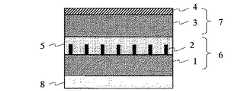
上記ディスプレイ用フィルターの構成を図1(模式断面図)に示す。図1において、プラスチックフィルム1に光吸収部2がストライプ状に平行に複数配列された外光遮蔽シート6と、プラスチックフィルム3に光学機能層4を有する光学フィルム7とが接着層5を介して貼合されており、かかる貼合は、外光遮蔽シート6の光吸収部2が形成されている面と光学フィルム7の光学機能層4とは反対面とが向き合うように、かつ接着層5が複数の光吸収部2の間を埋めるようになされている。 The configuration of the display filter is shown in FIG. 1 (schematic cross-sectional view). In FIG. 1, an external
かかるディスプレイ用フィルターは、光学機能層4が観賞側となるようにディスプレイパネルに接着層8を介して直接あるいはガラス板やプラスチック樹脂板を介して装着される。 Such a display filter is attached to the display panel directly or via a glass plate or a plastic resin plate so that the optical
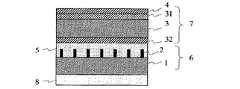
本発明のディスプレイ用フィルターの別の態様は、プラスチックフィルムの一方の面に光学機能層を有し、該プラスチックフィルムの他方の面に5〜50μmの高さを有する光吸収部がストライプ状に平行に複数配列され、その光吸収部が配列された面に複数の光吸収部の間を埋めるように接着層が積層されたものである。 図2に上記ディスプレイ用フィルターの模式断面図を示す。図2において、プラスチックフィルム11の一方の面に光学機能層12を有し、他方の面に光吸収部13がストライプ状に平行に複数配列され、複数の光吸収部13の間を埋めるように接着層14が積層されている。接着層14は、ディスプレイ用フィルターをディスプレイパネルに直接あるいはガラス板やプラスチック樹脂板を介して装着するための接着層として機能する。 In another aspect of the display filter of the present invention, an optical functional layer is provided on one surface of a plastic film, and light absorbing portions having a height of 5 to 50 μm are parallel to the other surface of the plastic film in stripes. And an adhesive layer is laminated on the surface on which the light absorption portions are arranged so as to fill the space between the plurality of light absorption portions. FIG. 2 is a schematic sectional view of the display filter. In FIG. 2, the
上述した本発明の2つの態様は、光吸収部と光吸収部との間の空隙を接着層で埋めることに特徴を有する。これによって、従来技術に比べディスプレイ用フィルターの製造工程が大幅に短縮され、更にディスプレイ用フィルターの層構成も簡略化される。 The two aspects of the present invention described above are characterized in that the gap between the light absorption part and the light absorption part is filled with an adhesive layer. As a result, the manufacturing process of the display filter is significantly shortened compared to the prior art, and the layer structure of the display filter is further simplified.
本発明のプラスチックフィルム上に突出した光吸収部の形成は、後述するように1つの工程で形成することが可能であり、従来の光吸収部の製造工程、即ち、樹脂から成る基盤層の形成、基盤層に楔形溝の形成、楔形溝に黒色物質を含む樹脂を充填することからなる製造工程に比べて大幅に製造工程が短縮できる。また、本発明のディスプレイ用フィルターは、外光遮蔽シートと光学フィルムとを貼り合わせるための接着層、あるいはディスプレイ用フィルターをディスプレイパネルに貼り合わせるための接着層を利用して、光吸収部と光吸収部の間の空隙を埋めるので、従来の層構成に比べて簡略化できる。 The light absorbing portion protruding on the plastic film of the present invention can be formed in one step as will be described later, and the conventional light absorbing portion manufacturing process, that is, the formation of the base layer made of resin. The manufacturing process can be greatly shortened compared to a manufacturing process comprising forming a wedge-shaped groove in the base layer and filling the wedge-shaped groove with a resin containing a black substance. In addition, the display filter of the present invention uses an adhesive layer for bonding the external light shielding sheet and the optical film, or an adhesive layer for bonding the display filter to the display panel. Since the gaps between the absorption parts are filled, it can be simplified as compared with the conventional layer structure.
次に、光吸収部の構成について説明する。光吸収部が配列されたプラスチックフィルムの平面図を図3に、図3のA−Aの模式断面図を図4に示す。プラスチックフィルム1上に光吸収部2が、水平方向(横方向)にストライプ状に多数形成されている。光吸収部2の高さhは、5〜50μmであり、好ましくは10〜30μmである。光吸収部2の幅wは、1〜10μmが好ましく、2〜8μmがより好ましい。光吸収部2と光吸収部2の間隔(ピッチ)pは、8〜50μmが好ましく、10〜30μmがより好ましい。光吸収部2のアスペクト比(h/w)は、2〜10の範囲が好ましく、3〜8の範囲がより好ましい。 Next, the configuration of the light absorption unit will be described. FIG. 3 is a plan view of the plastic film in which the light absorbing portions are arranged, and FIG. 4 is a schematic cross-sectional view taken along line AA of FIG. A large number of
上記の光吸収部の構成(幅、ピッチ、アスペクト比)にすることによって、光吸収部の高さhを比較的小さくしても、従来の光吸収部(高さ約100μm以上)と同程度の効果が得られ、更に光吸収部の高さを小さくすることによって凹凸の高低差が小さくなるので光吸収部への接着層の積層工程における問題点(例えば、気泡混入、接着層面の不均一、接着層の塗工欠陥等)を回避することが可能となる。 本発明において、光吸収部の形状は、図4に示すように断面が矩形であっても、台形(図5)あるいは三角形(図6)であってもよい。光吸収部の形状が台形及び三角形の場合のアスペクト比の計算には、底部の幅wを用いる。 By adopting the above configuration (width, pitch, aspect ratio) of the light absorbing portion, even if the height h of the light absorbing portion is relatively small, it is about the same as the conventional light absorbing portion (height of about 100 μm or more). In addition, since the height difference of the unevenness is reduced by reducing the height of the light absorbing portion, there are problems in the process of laminating the adhesive layer on the light absorbing portion (for example, mixing of bubbles, unevenness of the adhesive layer surface) , Coating defects in the adhesive layer, etc.) can be avoided. In the present invention, the shape of the light absorbing portion may be rectangular as shown in FIG. 4, trapezoid (FIG. 5), or triangle (FIG. 6). The width w of the bottom portion is used for calculating the aspect ratio when the light absorbing portion has a trapezoidal shape and a triangular shape.
本発明のプラスチックフィルムとは、ポリエステル、ポリオレフィン、環状ポリオレフィン、ポリアミド、トリアセチルセルロース、アクリル、ポリウレタンなどから構成されるフィルムを用いうるが、特にポリエステルフィルムが好ましい。ポリエステルフィルムのポリエステルとしては、ポリエチレンテレフタレート、ポリエチレンナフタレート、ポリプロピレンテレフタレート、ポリブチレンテレフタレートおよびポリプロピレンナフタレートなどが挙げられ、これらの2種以上が混合されたものであってもよい。また、これらと他のジカルボン酸成分やジオール成分が共重合されたポリエステルであってもよいが、この場合は、結晶配向が完了したフィルムにおいて、その結晶化度が好ましくは25%以上、より好ましくは30%以上、更に好ましくは35%以上のフィルムが好ましい。結晶化度が25%未満の場合には、寸法安定性や機械的強度が不十分となりやすい。結晶化度は、密度勾配法(JIS−K7112(1980))やラマンスペクトル分析法により得ることができる。 As the plastic film of the present invention, a film composed of polyester, polyolefin, cyclic polyolefin, polyamide, triacetyl cellulose, acrylic, polyurethane, or the like can be used, and a polyester film is particularly preferable. Examples of the polyester of the polyester film include polyethylene terephthalate, polyethylene naphthalate, polypropylene terephthalate, polybutylene terephthalate, and polypropylene naphthalate, and two or more of these may be mixed. Further, it may be a polyester in which these and other dicarboxylic acid components or diol components are copolymerized. In this case, in the film in which the crystal orientation is completed, the crystallinity is preferably 25% or more, more preferably Is preferably 30% or more, more preferably 35% or more. When the crystallinity is less than 25%, dimensional stability and mechanical strength tend to be insufficient. The crystallinity can be obtained by a density gradient method (JIS-K7112 (1980)) or a Raman spectrum analysis method.
上述したポリエステルを使用する場合には、その極限粘度(JIS K7367に従い、25℃のo−クロロフェノール中で測定)は、0.4〜1.2dl/gが好ましく、より好ましくは0.5〜0.8dl/gである。 When the above-described polyester is used, its intrinsic viscosity (measured in o-chlorophenol at 25 ° C. according to JIS K7367) is preferably 0.4 to 1.2 dl / g, more preferably 0.5 to 0.8 dl / g.
また、本発明で用いられるポリエステルフィルムは、2層以上の積層構造の複合体フィルムであっても良い。複合体フィルムとしては、例えば、内層部に実質的に粒子を含有せず、表層部に粒子を含有させた層を設けた複合体フィルムを挙げることができ、内層部と表層部が化学的に異種のポリマーであっても同種のポリマーであっても良い。本発明の目的用途であるディスプレイ用に用いる場合には、ポリエステルフィルム中には粒子などを含有しない方が内部散乱などがなく透明性などの光学特性上好ましい。 The polyester film used in the present invention may be a composite film having a laminated structure of two or more layers. As the composite film, for example, a composite film that is substantially free of particles in the inner layer portion and provided with a layer containing particles in the surface layer portion can be exemplified, and the inner layer portion and the surface layer portion are chemically separated. Different polymers or the same kind of polymers may be used. When used for a display which is the intended use of the present invention, the polyester film preferably does not contain particles or the like from the viewpoint of optical properties such as transparency without internal scattering.
本発明におけるポリエステルフィルムは、フィルムの熱安定性、特に寸法安定性や機械的強度を十分なものとし、平面性を良好にする観点から、ハードコート層が設けられた状態では二軸延伸により結晶配向されたフィルムであることが好ましい。二軸延伸により結晶配向しているとは、結晶配向が完了する前の熱可塑性樹脂フィルムを長手方向および/または幅方向にそれぞれ2.5〜5倍程度延伸し、その後熱処理により結晶配向を完了させたものであり、広角X線回折で二軸配向のパターンを示すものをいう。 In the present invention, the polyester film has sufficient thermal stability, particularly dimensional stability and mechanical strength, and from the viewpoint of improving the flatness, it is crystallized by biaxial stretching in a state where a hard coat layer is provided. An oriented film is preferred. The crystal orientation by biaxial stretching means that the thermoplastic resin film before the crystal orientation is completed is stretched about 2.5 to 5 times in the longitudinal direction and / or the width direction, and then the crystal orientation is completed by heat treatment. Which shows a biaxially oriented pattern by wide-angle X-ray diffraction.
ポリエステルフィルムの厚みは、特に限定するものでは無いが機械的強度やハンドリング性などの点から、好ましくは10〜500μm、より好ましくは20〜300μmである。 The thickness of the polyester film is not particularly limited, but is preferably 10 to 500 μm, more preferably 20 to 300 μm from the viewpoint of mechanical strength and handling properties.
ポリエステルフィルム中には本発明の効果を阻害しない範囲内で各種の添加剤や樹脂組成物、架橋剤などを含有しても良い。例えば酸化防止剤、耐熱安定剤、紫外線吸収剤、有機、無機の粒子(例えば例えばシリカ、コロイダルシリカ、アルミナ、アルミナゾル、カオリン、タルク、マイカ、炭酸カルシウム、硫酸バリウム、カーボンブラック、ゼオライト、酸化チタン、金属微粉末など)、顔料、染料、帯電防止剤、核剤、アクリル樹脂、ポリエステル樹脂、ウレタン樹脂、ポリオレフィン樹脂、ポリカーボネート樹脂、アルキッド樹脂、エポキシ樹脂、尿素樹脂、フェノール樹脂、シリコーン樹脂、ゴム系樹脂、ワックス組成物、メラミン系架橋剤、オキサゾリン系架橋剤、メチロール化、アルキロール化された尿素系架橋剤、アクリルアミド、ポリアミド、エポキシ樹脂、イソシアネート化合物、アジリジン化合物、各種シランカップリング剤、各種チタネート系カップリング剤などを挙げることができる。 The polyester film may contain various additives, resin compositions, cross-linking agents and the like within a range that does not impair the effects of the present invention. For example, antioxidants, heat stabilizers, ultraviolet absorbers, organic and inorganic particles (for example, silica, colloidal silica, alumina, alumina sol, kaolin, talc, mica, calcium carbonate, barium sulfate, carbon black, zeolite, titanium oxide, Metal fine powders), pigments, dyes, antistatic agents, nucleating agents, acrylic resins, polyester resins, urethane resins, polyolefin resins, polycarbonate resins, alkyd resins, epoxy resins, urea resins, phenol resins, silicone resins, rubber resins , Wax composition, melamine crosslinking agent, oxazoline crosslinking agent, methylolated, alkylolized urea crosslinking agent, acrylamide, polyamide, epoxy resin, isocyanate compound, aziridine compound, various silane coupling agents, various titanates And the like can be mentioned system coupling agent.
特にプラズマディスプレイ用に使用する場合には、色補正や近赤外カット機能を有する染料を用いるためにポリエステルフィルムには紫外線カット機能を有するのが好ましく、紫外線吸収剤を含有させるのが好ましい。 Particularly when used for a plasma display, the polyester film preferably has an ultraviolet cut function and preferably contains an ultraviolet absorber in order to use a dye having a color correction function and a near infrared cut function.
紫外線吸収剤としては、例えばサリチル酸系化合物、ベンゾフェノン系化合物、ベンゾトリアゾール系化合物、シアノアクリレート系化合物、およびベンゾオキサジノン系化合物、環状イミノエステル系化合物などを好ましく例示することができるが380nm〜390nmでの紫外線カット性、色調などの点からベンゾオキサジノン系化合物が最も好ましい。これらの化合物は1種で用いても良いし、2種以上併用しても良い。またHALS(ヒンダードアミン系光安定剤)や酸化防止剤などの安定剤の併用はより好ましい。 Preferred examples of the ultraviolet absorber include salicylic acid compounds, benzophenone compounds, benzotriazole compounds, cyanoacrylate compounds, benzoxazinone compounds, cyclic imino ester compounds, and the like. Of these, benzoxazinone compounds are most preferred from the viewpoints of UV-cutting property and color tone. These compounds may be used alone or in combination of two or more. Moreover, combined use of stabilizers, such as HALS (hindered amine light stabilizer) and antioxidant, is more preferable.
好ましい材料であるベンゾオキサジノン系化合物の例としては、2−p−ニトロフェニル−3,1−ベンゾオキサジン−4−オン、2−(p−ベイゾイルフェニル)−3,1−ベンゾオキサジン−4−オン、2−(2−ナフチル)−3,1−ベンゾオキサジン−4−オン、2−2´−p−フェニレンビス(3,1−ベンゾオキサジン−4−オン)、2,2´−(2,6−ナフチレン)ビス(3,1−ベンゾオキサジン−4−オン)などを例示することができる。これらの化合物の添加量は基材フィルム中に0.5〜5重量%好ましくは1〜5重量%含有させるのが好ましい。 Examples of benzoxazinone-based compounds that are preferable materials include 2-p-nitrophenyl-3,1-benzoxazin-4-one and 2- (p-bezoylphenyl) -3,1-benzoxazine-4. -One, 2- (2-naphthyl) -3,1-benzoxazin-4-one, 2-2'-p-phenylenebis (3,1-benzoxazin-4-one), 2,2 '-( 2,6-naphthylene) bis (3,1-benzoxazin-4-one) and the like can be exemplified. The amount of these compounds added is preferably 0.5 to 5% by weight, preferably 1 to 5% by weight, in the base film.
また、更に優れた耐光性を付与するためにシアノアクリレート系4量体化合物を併用することが好ましい。シアノアクリレート系4量体化合物は基材フィルム中に0.05〜2重量%含有させることが好ましい。シアノアクリレート系4量体化合物とは、シアノアクリレートの4量体を基本とする化合物であり、例えば1,3−ビス(2´シアノ−3,3−ジフェニルアクリロイルオキシ)−2、2−ビス−(2´シアノ−3,3−ジフェニルアクリロイルオキシメチルプロパン)などを例示することができる。これと併用する場合には、前述の紫外線吸収剤は基材フィルム中に0.3〜3重量%添加するのが好適である。 Further, it is preferable to use a cyanoacrylate-based tetramer compound in combination in order to impart further excellent light resistance. The cyanoacrylate tetramer compound is preferably contained in the base film in an amount of 0.05 to 2% by weight. The cyanoacrylate-based tetramer compound is a compound based on a tetramer of cyanoacrylate, such as 1,3-bis (2′cyano-3,3-diphenylacryloyloxy) -2, 2-bis-. (2 ′ cyano-3,3-diphenylacryloyloxymethylpropane) and the like can be exemplified. When using together with this, it is suitable to add 0.3 to 3 weight% of the above-mentioned ultraviolet absorber in a base film.
上記の紫外線吸収剤添加による本発明の基材プラスチックフィルムは波長380nmでの透過率が5%以下、好ましくは3%以下であるのが望ましく、これにより特にプラズマディスプレイ用部材に適用した場合、紫外線から基材フィルムや染料色素などを保護することができる。上記の透過率は、分光光度計U−3410((株)日立製作所製)に直径60mmの積分球130−063((株)日立製作所製)及び10度傾斜スペーサーを取り付けた状態で波長380nmの透過率を求めることができる。本発明に用いられるプラスチックフィルムは、光学機能層、ハードコート層、あるいは後述する導電層や近赤外線遮蔽層との密着性(接着強度)を強化のための下引き層(プライマー層)を設けておくのが好ましい。下引き層はフィルム製膜中に塗布するインラインコーティング法によるのが経済性の点から好ましく、ポリエステル共重合体、アクリル共重合体、各種ウレタン、メラミン、ポリアミド、エポキシなどから選択することができ、これらを公知の方法で架橋剤などを添加して接着性向上や耐溶剤性向上などの特性を賦与することができる。 It is desirable that the base plastic film of the present invention by adding the above ultraviolet absorber has a transmittance at a wavelength of 380 nm of 5% or less, preferably 3% or less. Therefore, it is possible to protect the base film and dye pigment. The transmittance is 380 nm with a spectrophotometer U-3410 (manufactured by Hitachi, Ltd.) and an integrating sphere 130-063 (manufactured by Hitachi, Ltd.) having a diameter of 60 mm and a 10 degree tilt spacer attached. The transmittance can be determined. The plastic film used in the present invention is provided with an undercoat layer (primer layer) for enhancing the adhesion (adhesive strength) with the optical functional layer, the hard coat layer, or a conductive layer and a near-infrared shielding layer described later. It is preferable to leave. The undercoating layer is preferably from an in-line coating method applied during film formation from the economical point of view, and can be selected from polyester copolymers, acrylic copolymers, various urethanes, melamines, polyamides, epoxies, etc. These can be imparted with characteristics such as improved adhesion and improved solvent resistance by adding a crosslinking agent or the like by a known method.
光吸収部は、マトリックス組成物に着色剤を分散あるいは溶解したもので形成することができる。マトリックス組成物としては、紫外線や電子線等の電離放射線で硬化する樹脂、オリゴマー、モノマーおよびこれらの混合体、熱硬化性組成物等の硬化性樹脂を用いることができる。特に電離放射線硬化組成物は硬化速度が早く生産性に優れ、かつ光吸収層を被覆する際の塗布組成物およびそれに使用する溶剤などに対する耐久性に優れるので好ましい。 The light absorbing portion can be formed by dispersing or dissolving a colorant in the matrix composition. As the matrix composition, a curable resin such as a resin, an oligomer, a monomer and a mixture thereof, or a thermosetting composition that is cured by ionizing radiation such as ultraviolet rays or an electron beam can be used. In particular, the ionizing radiation curable composition is preferable because it has a high curing rate and excellent productivity, and is excellent in durability to a coating composition and a solvent used in coating the light absorbing layer.
電離放射線硬化性樹脂、オリゴマー、モノマーとしては、分子内にエチレン性不飽和二重結合を含有する組成物であり特に限定するものではない。具体的には1〜3個のエチレン性不飽和二重結合を有する組成物、4個以上のエチレン性不飽和二重結合を有する組成物などを挙げることができるが、ストライプ形状の精度、耐傷性などを考慮するとその主成分として多官能アクリレートを用いるのが好ましい。多官能アクリレートとは、1分子中に3(より好ましくは4、更に好ましくは5)個以上の(メタ)アクリロイルオキシ基を有する単量体もしくはオリゴマー、プレポリマーであって、1分子中に3個以上の(メタ)アクリロイルオキシ基(但し、本明細書において「・・・(メタ)アクリ・・・」とは、「・・・アクリ・・・又は・・・メタアクリ・・・」を略して表示したものである。)を有する単量体、オリゴマー、プレポリマーを言う。このような組成物としては、1分子中に3個以上のアルコール性水酸基を有する多価アルコールの該水酸基が、3個以上の(メタ)アクリル酸のエステル化物となっている化合物などを挙げることができる。 The ionizing radiation curable resin, oligomer and monomer are compositions containing an ethylenically unsaturated double bond in the molecule and are not particularly limited. Specific examples include a composition having 1 to 3 ethylenically unsaturated double bonds, a composition having 4 or more ethylenically unsaturated double bonds, and the like. Considering the properties and the like, it is preferable to use a polyfunctional acrylate as the main component. The polyfunctional acrylate is a monomer, oligomer or prepolymer having 3 (more preferably 4, more preferably 5) or more (meth) acryloyloxy groups in one molecule, and 3 in one molecule. More than one (meth) acryloyloxy group (in the present specification, "... (meth) acryl ..." means "... acrylic ... or ... metaacryl ...") Monomer, oligomer, and prepolymer. Examples of such a composition include compounds in which the hydroxyl group of a polyhydric alcohol having 3 or more alcoholic hydroxyl groups in one molecule is an esterified product of 3 or more (meth) acrylic acids. Can do.
具体的な例としては、ペンタエリスリトールトリ(メタ)アクリレート、ペンタエリスリトールテトラ(メタ)アクリレート、ジペンタエリスリトールトリ(メタ)アクリレート、ジペンタエリスリトールテトラ(メタ)アクリレート、ジペンタエリスリトールペンタ(メタ)アクリレート、ジペンタエリスリトールヘキサ(メタ)アクリレート、トリメチロールプロパントリ(メタ)アクリレート、ペンタエリスリトールトリアクリレートヘキサメチレンジイソシアネートウレタンプレポリマー、ペンタエリスリトールトリアクリレートトルエンジイソシアネートウレタンプレポリマー、ペンタエリスリトールトリアクリレートイソホロンジイソシアネートウレタンプレポリマーなどを用いることができる。これらは、1種または2種以上を混合して使用することができる。 Specific examples include pentaerythritol tri (meth) acrylate, pentaerythritol tetra (meth) acrylate, dipentaerythritol tri (meth) acrylate, dipentaerythritol tetra (meth) acrylate, dipentaerythritol penta (meth) acrylate, Dipentaerythritol hexa (meth) acrylate, trimethylolpropane tri (meth) acrylate, pentaerythritol triacrylate hexamethylene diisocyanate urethane prepolymer, pentaerythritol triacrylate toluene diisocyanate urethane prepolymer, pentaerythritol triacrylate isophorone diisocyanate urethane prepolymer, etc. Can be used. These may be used alone or in combination of two or more.
これらの1分子中に3個以上の(メタ)アクリロイルオキシ基を有する単量体、オリゴマー、プレポリマーの使用割合は構成成分総量に対して50〜90重量%が好ましく、より好ましくは50〜80重量%である。 The proportion of the monomer, oligomer or prepolymer having 3 or more (meth) acryloyloxy groups in one molecule is preferably 50 to 90% by weight, more preferably 50 to 80%, based on the total amount of the constituent components. % By weight.
上記の化合物以外に剛直性を緩和させたり、硬化時の収縮を緩和させたり、塗液の粘度を調整する目的で1〜2官能のアクリレートを併用するのが好ましい。
1分子中に1〜2個のエチレン性不飽和二重結合を有する単量体としては、ラジカル重合性のある通常の単量体ならば特に限定されずに使用することができる。In addition to the above compounds, it is preferable to use one or two functional acrylates together for the purpose of relaxing the rigidity, relaxing the shrinkage during curing, or adjusting the viscosity of the coating liquid.
The monomer having 1 to 2 ethylenically unsaturated double bonds in one molecule can be used without particular limitation as long as it is a normal monomer having radical polymerizability.
分子内に2個のエチレン性不飽和二重結合を有する化合物としては、下記(a)〜(f)の(メタ)アクリレート等を用いることができる。すなわち、(a)炭素数2〜12のアルキレングリコールの(メタ)アクリル酸ジエステル類:エチレングリコールジ(メタ)アクリレート、プロピレングリコールジ(メタ)アクリレート、1,4−ブタンジオールジ(メタ)アクリレート、ネオペンチルグリコールジ(メタ)アクリレート、1,6−ヘキサンジオールジ(メタ)アクリレートなど、
(b)ポリオキシアルキレングリコールの(メタ)アクリレート酸ジエステル類:ジエチレングリコールジ(メタ)アクリレート、トリエチレングリコールジ(メタ)アクリレート、テトラエチレングリコールジ(メタ)アクリレート、ジプロピレングリコールジ(メタ)アクリレート、ポリエチレングリコールジ(メタ)アクリレート、ポリプロピレングリコールジ(メタ)アクリレートなど、
(c)多価アルコールの(メタ)アクリル酸ジエステル類:ペンタエリスリトールジ(メタ)アクリレートなど、
(d)ビスフェノールAあるいはビスフェノールAの水素化物のエチレンオキシド及びプロピレンオキシド付加物の(メタ)アクリル酸ジエステル類:2,2’−ビス(4−アクリロキシエトキシフェニル)プロパン、2,2’−ビス(4−アクリロキシプロポキシフェニル)プロパンなど、
(e)ジイソシアネート化合物と2個以上のアルコール性水酸基含有化合物を予め反応させて得られる末端イソシアネート基含有化合物に、更にアルコール性水酸基含有(メタ)アクリレートを反応させて得られる分子内に2個以上の(メタ)アクリロイルオキシ基を有するウレタン(メタ)アクリレート類など、および、
(f)分子内に2個以上のエポキシ基を有する化合物にアクリル酸又はメタクリル酸を反応させて得られる分子内に2個以上の(メタ)アクリロイルオキシ基を有するエポキシ(メタ)アクリレート類など。As the compound having two ethylenically unsaturated double bonds in the molecule, the following (a) to (f) (meth) acrylates and the like can be used. (A) (meth) acrylic acid diesters of alkylene glycol having 2 to 12 carbon atoms: ethylene glycol di (meth) acrylate, propylene glycol di (meth) acrylate, 1,4-butanediol di (meth) acrylate, Neopentyl glycol di (meth) acrylate, 1,6-hexanediol di (meth) acrylate, etc.
(B) (Meth) acrylate diesters of polyoxyalkylene glycol: diethylene glycol di (meth) acrylate, triethylene glycol di (meth) acrylate, tetraethylene glycol di (meth) acrylate, dipropylene glycol di (meth) acrylate, Polyethylene glycol di (meth) acrylate, polypropylene glycol di (meth) acrylate, etc.
(C) Polyhydric alcohol (meth) acrylic acid diesters: pentaerythritol di (meth) acrylate, etc.
(D) (Meth) acrylic acid diesters of ethylene oxide and propylene oxide adducts of bisphenol A or bisphenol A hydride: 2,2′-bis (4-acryloxyethoxyphenyl) propane, 2,2′-bis ( 4-acryloxypropoxyphenyl) propane, etc.
(E) Two or more in a molecule obtained by reacting a terminal isocyanate group-containing compound obtained by reacting a diisocyanate compound and two or more alcoholic hydroxyl group-containing compounds in advance with an alcoholic hydroxyl group-containing (meth) acrylate. Urethane (meth) acrylates having a (meth) acryloyloxy group, and the like, and
(F) Epoxy (meth) acrylates having two or more (meth) acryloyloxy groups in the molecule obtained by reacting a compound having two or more epoxy groups in the molecule with acrylic acid or methacrylic acid.
分子内に1個のエチレン性不飽和二重結合を有する化合物としては、メチル(メタ)アクリレート、エチル(メタ)アクリレート、n−及びi−プロピル(メタ)アクリレート、n−、sec−、およびt−ブチル(メタ)アクリレート、2−エチルヘキシル(メタ)アクリレート、ラウリル(メタ)アクリレート、ステアリル(メタ)アクリレート、メトキシエチル(メタ)アクリレート、エトキシエチル(メタ)アクリレート、ヒドロキシエチル(メタ)アクリレート、ポリエチレングリコールモノ(メタ)アクリレート、ポリプロピレングリコールモノ(メタ)アクリレート、グリシジル(メタ)アクリレート、テトラヒドロフルフリル(メタ)アクリレート、N−ヒドロキシエチル(メタ)アクリルアミド、N−ビニルピロリドン、N−ビニル−3−メチルピロリドン、N−ビニル−5−メチルピロリドンなどを用いることができる。これらの単量体は、1種または2種以上混合して使用してもよい。 Compounds having one ethylenically unsaturated double bond in the molecule include methyl (meth) acrylate, ethyl (meth) acrylate, n- and i-propyl (meth) acrylate, n-, sec-, and t. -Butyl (meth) acrylate, 2-ethylhexyl (meth) acrylate, lauryl (meth) acrylate, stearyl (meth) acrylate, methoxyethyl (meth) acrylate, ethoxyethyl (meth) acrylate, hydroxyethyl (meth) acrylate, polyethylene glycol Mono (meth) acrylate, polypropylene glycol mono (meth) acrylate, glycidyl (meth) acrylate, tetrahydrofurfuryl (meth) acrylate, N-hydroxyethyl (meth) acrylamide, N-vinylpyrrolidone, - vinyl-3-methylpyrrolidone, or the like can be used N- vinyl-5-methyl pyrrolidone. These monomers may be used alone or in combination of two or more.
これらの1分子中に1〜2個のエチレン性不飽和二重結合を有する単量体の使用割合は、構成成分総量に対して10〜40重量%が好ましく、より好ましくは20〜40重量%である。アクリルオリゴマーとは、アクリル系樹脂骨格に反応性のアクリル基が結合されたもの、ポリエステルアクリレート、ウレタンアクリレート、エポキシアクリレートおよびポリエーテルアクリレートなどであり、また、メラミンやイソシアヌール酸などの剛直な骨格にアクリル基を結合したものなども用い得る。 The proportion of the monomer having 1 to 2 ethylenically unsaturated double bonds in one molecule is preferably 10 to 40% by weight, more preferably 20 to 40% by weight based on the total amount of the constituent components. It is. Acrylic oligomers are those in which a reactive acrylic group is bonded to an acrylic resin skeleton, such as polyester acrylate, urethane acrylate, epoxy acrylate, and polyether acrylate. In addition, a rigid skeleton such as melamine or isocyanuric acid is used. Those having an acrylic group bonded thereto can also be used.
これらの材料により構成された塗剤の粘度は1000〜5000mPa・s(25℃)、加温時には50〜200mPa・s(100℃)であることが形状をコントロールしやすくなるので好ましい。これらのアクリルオリゴマーなどの具体例は、山下晋三、金子東助編、「架橋剤ハンドブック」、大成社1981年発行、第267頁から第275頁、第562頁から第593頁を参考とすることができる。また、市販されている多官能アクリル系硬化塗料としては三菱レイヨン株式会社;(商品名“ダイヤビーム”シリーズなど)、長瀬産業株式会社;(商品名“デナコール”シリーズなど)、新中村株式会社;(商品名“NKエステル”シリーズなど)、大日本インキ化学工業株式会社;(商品名“UNIDIC”シリーズなど)、東亜合成化学工業株式会社;(商品名“アロニックス”シリーズなど)、日本油脂株式会社;(商品名“ブレンマー”シリーズなど)、日本化薬株式会社;(商品名“KAYARAD”シリーズなど)、共栄社化学株式会社;(商品名“ライトエステル”シリーズ、“ライトアクリレート”シリーズなど)、JSR株式会社;(商品名“デソライト”シリーズ)などの製品を利用することができる。 The viscosity of the coating material composed of these materials is preferably 1000 to 5000 mPa · s (25 ° C.) and 50 to 200 mPa · s (100 ° C.) at the time of heating because the shape can be easily controlled. For specific examples of these acrylic oligomers, etc., refer to Shinzo Yamashita, Tosuke Kaneko, “Crosslinking Agent Handbook”, Taiseisha 1981, pages 267 to 275, pages 562 to 593. Can do. Commercially available polyfunctional acrylic cured paints include Mitsubishi Rayon Co., Ltd. (trade name “Diabeam” series, etc.), Nagase Sangyo Co., Ltd. (trade name “Denacol” series, etc.), Shin-Nakamura Co., Ltd .; (Product name “NK Ester” series, etc.), Dainippon Ink and Chemicals Co., Ltd .; (Product name “UNIDIC” series, etc.), Toa Gosei Chemical Industries Co., Ltd. (product name “Aronix” series, etc.), Nippon Oils and Fats Co., Ltd. (Trade name “Blemmer” series, etc.), Nippon Kayaku Co., Ltd .; (trade name “KAYARAD” series, etc.), Kyoeisha Chemical Co., Ltd. (trade names “light ester” series, “light acrylate” series, etc.), JSR Co., Ltd. (trade name “Desolite” series) can be used.
また、光吸収部のマトリックス組成物中に改質剤を含有させることができる。改質剤として、塗布性改良剤、消泡剤、増粘剤、帯電防止剤、無機系粒子、有機系粒子、有機系潤滑剤、有機高分子化合物、紫外線吸収剤、光安定剤、染料、顔料あるいは安定剤などを用いることができ、これらは活性線または熱による反応を損なわない範囲内で構成する塗布層の組成物成分として使用され、用途に応じて特性を改良することができる。 Moreover, a modifier can be contained in the matrix composition of the light absorption part. As modifiers, coatability improvers, antifoaming agents, thickeners, antistatic agents, inorganic particles, organic particles, organic lubricants, organic polymer compounds, UV absorbers, light stabilizers, dyes, A pigment, a stabilizer, or the like can be used, and these are used as a composition component of a coating layer formed within a range that does not impair an actinic ray or heat reaction, and the properties can be improved according to applications.
電離放射線の種類、例えば紫外線を用いる場合などは、従来公知の光重合開始剤を用いるのが好ましい。 In the case of using ionizing radiation, for example, ultraviolet rays, it is preferable to use a conventionally known photopolymerization initiator.
光吸収部の着色剤としては、黒色顔料等の各種顔料や染料が用いることができる。黒色顔料としては、カーボンブラック、チタンや鉄等の黒色金属粒子等が挙げられる。黒色顔料以外の青色、紫色、黄色、赤色の各種顔料及び/又は染料を単独あるいは混合して用いることができる。着色剤の含有量は、光吸収部のマトリックス組成物に対して1〜50質量%の範囲が適当である。 As the colorant for the light absorbing portion, various pigments such as black pigments and dyes can be used. Examples of the black pigment include carbon black, black metal particles such as titanium and iron, and the like. Various pigments and / or dyes of blue, purple, yellow and red other than black pigments can be used alone or in combination. The content of the colorant is suitably in the range of 1 to 50% by mass with respect to the matrix composition of the light absorbing part.
本発明のディスプレイ用フィルターを構成する光学機能層は、反射防止層、防眩層、あるいは反射防止機能と防眩機能を兼ね備えた層である。光学機能層は単一層であっても複数層で構成されていてもよい。以下、光学機能層について詳細に説明する。 The optical functional layer constituting the display filter of the present invention is an antireflection layer, an antiglare layer, or a layer having both an antireflection function and an antiglare function. The optical functional layer may be a single layer or a plurality of layers. Hereinafter, the optical functional layer will be described in detail.
反射防止層は、ディスプレイの画像表示に影響を与える蛍光灯などの外光の反射や映り込みを防止するものである。反射防止層は、表面の視感反射率が5%以下であることが好ましく、4%以下がより好ましく、特に3%以下であることが好ましい。ここで視感反射率は、分光光度計等を使用して可視領域波長(380〜780nm)の反射率を測定し、CIE1931システムに準じて計算された視感反射率(Y)である。 The antireflection layer prevents reflection or reflection of external light such as a fluorescent lamp that affects the image display on the display. The antireflection layer preferably has a surface luminous reflectance of 5% or less, more preferably 4% or less, and particularly preferably 3% or less. Here, the luminous reflectance is a luminous reflectance (Y) calculated according to the CIE1931 system by measuring the reflectance in the visible region wavelength (380 to 780 nm) using a spectrophotometer or the like.
このような反射防止層としては、高屈折率層と低屈折率層とを低屈折率層が視認側になるように2層以上積層したものを用いることが好ましい。高屈折率層の屈折率は1.5〜1.7の範囲が好ましく、特に1.55〜1.69の範囲が好ましい。低屈折率層の屈折率は1.25〜1.49の範囲が好ましく、特に1.3〜1.45の範囲が好ましい。 As such an antireflection layer, it is preferable to use a layer in which two or more layers of a high refractive index layer and a low refractive index layer are laminated so that the low refractive index layer is on the viewing side. The refractive index of the high refractive index layer is preferably in the range of 1.5 to 1.7, particularly preferably in the range of 1.55 to 1.69. The refractive index of the low refractive index layer is preferably in the range of 1.25 to 1.49, particularly preferably in the range of 1.3 to 1.45.
高屈折率層を形成する材料としては、上述した光吸収部の形成に用いられる組成物と同様のもの、あるいは酸化インジウムを主成分としこれに二酸化チタンなどを少量含ませたもの、あるいはAl2O3、MgO、TiO2等の無機系材料が挙げられる。特に上記光吸収部の形成に用いられる組成物中に金属酸化物粒子を分散配合する方法が屈折率の向上と帯電防止効果の両立が可能となるので特に好ましい。金属酸化物微粒子としては錫含有酸化アンチモン粒子(ATO)、亜鉛含有酸化アンチモン粒子、錫含有酸化インジウム粒子(ITO)、酸化亜鉛/酸化アルミニウム粒子、酸化アンチモン粒子等が好ましく、より好ましくは錫含有酸化インジウム粒子(ITO)、錫含有酸化アンチモン粒子(ATO)である。As a material for forming the high refractive index layer, the same composition as that used for forming the light absorbing portion described above, a material mainly containing indium oxide and containing a small amount of titanium dioxide or the like, or Al2 Examples thereof include inorganic materials such as O3 , MgO, and TiO2 . In particular, a method of dispersing and blending metal oxide particles in the composition used for forming the light absorbing portion is particularly preferable because it is possible to improve both the refractive index and the antistatic effect. As the metal oxide fine particles, tin-containing antimony oxide particles (ATO), zinc-containing antimony oxide particles, tin-containing indium oxide particles (ITO), zinc oxide / aluminum oxide particles, antimony oxide particles, etc. are preferable, and tin-containing oxidation is more preferable. Indium particles (ITO) and tin-containing antimony oxide particles (ATO).
かかる金属酸化物粒子は、平均粒子径(JIS R1626に示されるBET法により測定される球相当径(JIS Z8819−1にて定義))が0.5μm以下の粒子が好適に使用されるが、より好ましくは、0.001〜0.3μm、更に好ましくは0.005〜0.2μmの粒子径のものが用いられる。該平均粒子径が、この範囲を超えると高屈折率層の透明性を低下させ、この範囲未満では、該粒子が凝集し易くヘイズ値が増大する場合がある。金属酸化物粒子の含有量は、樹脂成分に対して、0.1〜20質量%の範囲が好ましい。 As such metal oxide particles, particles having an average particle size (sphere equivalent diameter measured by the BET method shown in JIS R1626 (defined in JIS Z8819-1)) of 0.5 μm or less are preferably used. More preferably, those having a particle size of 0.001 to 0.3 μm, and more preferably 0.005 to 0.2 μm are used. When the average particle diameter exceeds this range, the transparency of the high refractive index layer is lowered. When the average particle diameter is less than this range, the particles tend to aggregate and the haze value may increase. The content of the metal oxide particles is preferably in the range of 0.1 to 20% by mass with respect to the resin component.
高屈折率層には、更にカルボキシル基、リン酸基、スルホン酸基等の酸性官能基を有する(メタ)アクリレート化合物(モノマー)を使用することができる。具体的には、酸性官能基含有モノマーとしては、アクリル酸、メタクリル酸、クロトン酸、2−(メタ)アクリロイルオキシエチルコハク酸、2−(メタ)アクリロイルオキシエチルフタル酸などの不飽和カルボン酸、モノ(2−(メタ)アクリロイルオキシエチル)アシッドホスフェート、ジフェニル−2−(メタ)アクリロイルオキシエチルホスフェート等のリン酸(メタ)アクリル酸エステル、2−スルホエステル(メタ)アクリレート等が挙げられる。その他、アミド結合、ウレタン結合、エーテル結合などの極性を持った結合を有する(メタ)アクリレート化合物を使用することができる。 In the high refractive index layer, a (meth) acrylate compound (monomer) having an acidic functional group such as a carboxyl group, a phosphoric acid group, or a sulfonic acid group can be used. Specifically, as the acidic functional group-containing monomer, unsaturated carboxylic acid such as acrylic acid, methacrylic acid, crotonic acid, 2- (meth) acryloyloxyethyl succinic acid, 2- (meth) acryloyloxyethylphthalic acid, Examples thereof include phosphoric acid (meth) acrylic acid esters such as mono (2- (meth) acryloyloxyethyl) acid phosphate and diphenyl-2- (meth) acryloyloxyethyl phosphate, and 2-sulfoester (meth) acrylate. In addition, a (meth) acrylate compound having a polar bond such as an amide bond, a urethane bond, or an ether bond can be used.
高屈折率層には、塗布した組成物の硬化を進めるために開始剤を使用してもよい。該開始剤としては、塗布した組成物を、ラジカル反応、アニオン反応、カチオン反応等による重合および/または架橋反応を開始あるいは促進せしめるものであり、従来から公知の各種光重合開始剤が使用可能である。かかる光重合開始剤としては、具体的には、ソジウムメチルジチオカーバメイトサルファイド、ジフェニルモノサルファイド、ジベンゾチアゾイルモノサルファイド及びジサルファイド等のサルファイド類や、チオキサントン、2−エチルチオキサントン、2−クロロチオキサントン、2,4−ジエチルチオキサントン等のチオキサントン誘導体や、ヒドラゾン、アゾビスイソブチロニトリル等のアゾ化合物や、ベンゼンジアゾニウム塩等のジアゾ化合物や、ベンゾイン、ベンゾインメチルエーテル、ベンゾインエチルエーテル、ベンゾフェノン、ジメチルアミノベンゾフェノン、ミヒラーケトン、ベンジルアントラキノン、t−ブチルアントラキノン、2−メチルアントラキノン、2−エチルアントラキノン、2−アミノアントラキノン、2−クロロアントラキノン等の芳香族カルボニル化合物や、p−ジメチルアミノ安息香酸メチル、p−ジメチルアミノ安息香酸エチル、D−ジメチルアミノ安息香酸ブチル、p−ジエチルアミノ安息香酸イソプロピル等のジアルキルアミノ安息香酸エステルや、ベンゾイルパーオキサイド、ジ−t−ブチルパーオキサイド、ジクミルパーオキサイド、クメンハイドロパーオキサイド等の過酸化物や、9−フェニルアクリジン、9−p−メトキシフェニルアクリジン、9−アセチルアミノアクリジン、ベンズアクリジン等のアクリジン誘導体や、9,10−ジメチルベンズフェナジン、9−メチルベンズフェナジン、10−メトキシベンズフェナジン等のフェナジン誘導体や、6,4’,4”−トリメトキシ−2、3−ジフェニルキノキサリン等のキノキサリン誘導体や、2,4,5−トリフェニルイミダゾイル二量体、2−ニトロフルオレン、2,4,6−トリフェニルピリリウム四弗化ホウ素塩、2,4,6−トリス(トリクロロメチル)−1,3,5−トリアジン、3,3’−カルボニルビスクマリン、チオミヒラーケトン、2,4,6−トリメチルベンゾイルジフェニルフォスフィンオキシド、オリゴ(2−ヒドロキシ−2−メチル−1−(4−(1−メチルビニル)フェニル)プロパノン、2−ベンジル−2−ジメチルアミノ−1−(4−モルホリノフェニル)−ブタノン等が挙げられる。 An initiator may be used for the high refractive index layer in order to advance the curing of the applied composition. As the initiator, the applied composition initiates or accelerates polymerization and / or crosslinking reaction by radical reaction, anion reaction, cation reaction, etc., and various conventionally known photopolymerization initiators can be used. is there. Specific examples of such photopolymerization initiators include sulfides such as sodium methyldithiocarbamate sulfide, diphenyl monosulfide, dibenzothiazoyl monosulfide and disulfide, thioxanthone, 2-ethylthioxanthone, 2-chlorothioxanthone, Thioxanthone derivatives such as 2,4-diethylthioxanthone, azo compounds such as hydrazone and azobisisobutyronitrile, diazo compounds such as benzenediazonium salt, benzoin, benzoin methyl ether, benzoin ethyl ether, benzophenone, dimethylaminobenzophenone Michler's ketone, benzylanthraquinone, t-butylanthraquinone, 2-methylanthraquinone, 2-ethylanthraquinone, 2-aminoanthraquinone, Aromatic carbonyl compounds such as -chloroanthraquinone, dialkylaminobenzoic acid esters such as methyl p-dimethylaminobenzoate, ethyl p-dimethylaminobenzoate, butyl D-dimethylaminobenzoate, isopropyl p-diethylaminobenzoate, Peroxides such as benzoyl peroxide, di-t-butyl peroxide, dicumyl peroxide, cumene hydroperoxide, 9-phenylacridine, 9-p-methoxyphenylacridine, 9-acetylaminoacridine, benzacridine, etc. Acridine derivatives, phenazine derivatives such as 9,10-dimethylbenzphenazine, 9-methylbenzphenazine, 10-methoxybenzphenazine, and 6,4 ′, 4 ″ -trimethoxy-2,3-diphenylquinoxaline Quinoxaline derivatives, 2,4,5-triphenylimidazolyl dimer, 2-nitrofluorene, 2,4,6-triphenylpyrylium tetrafluoride boron salt, 2,4,6-tris (trichloromethyl) ) -1,3,5-triazine, 3,3′-carbonylbiscoumarin, thiomichler ketone, 2,4,6-trimethylbenzoyldiphenylphosphine oxide, oligo (2-hydroxy-2-methyl-1- ( 4- (1-methylvinyl) phenyl) propanone, 2-benzyl-2-dimethylamino-1- (4-morpholinophenyl) -butanone, and the like.
また、高屈折率層には、上記開始剤の酸素阻害による感度の低下を防止するために、光重合開始剤にアミン化合物を共存させてもよい。このようなアミン化合物としては、例えば、脂肪族アミン化合物や、芳香族アミン化合物等の不揮発性のものであれば、特に限定されないが、例えば、トリエタノールアミン、メチルジエタノールアミン等が適切である。 In the high refractive index layer, an amine compound may coexist in the photopolymerization initiator in order to prevent a decrease in sensitivity due to oxygen inhibition of the initiator. Such an amine compound is not particularly limited as long as it is a non-volatile compound such as an aliphatic amine compound or an aromatic amine compound. For example, triethanolamine, methyldiethanolamine and the like are suitable.
更に、高屈折率層には、重合禁止剤、硬化触媒、酸化防止剤、分散剤等の各種添加剤を含有することができる。 Furthermore, the high refractive index layer can contain various additives such as a polymerization inhibitor, a curing catalyst, an antioxidant, and a dispersant.
高屈折率層の厚みは、0.05〜20μmの範囲が好ましく、0.1〜10μmの範囲がより好ましい。 The thickness of the high refractive index layer is preferably in the range of 0.05 to 20 μm, and more preferably in the range of 0.1 to 10 μm.
反射防止層を構成する低屈折率層は、含フッ素系組成物が好ましく具体的な一例を挙げれば(メタ)アクリル酸の部分または完全フッ素化アルキルエステル、含フッ素シリコーン等の有機系材料、MgF2、CaF2など。またSiO2等の無機系材料で構成することができ、特に内部に空洞を有する中空シリカは空気相の存在により低屈折率化できるので特に好ましい。以下に低屈折率層の好ましい態様を例示する。The low refractive index layer constituting the antireflection layer is preferably a fluorine-containing composition, and specific examples include a (meth) acrylic acid portion or a fully fluorinated alkyl ester, an organic material such as fluorine-containing silicone, MgF2 , CaF2 etc. Also it can be composed of an inorganic material such as SiO2, especially preferred because especially hollow silica having a cavity therein may lower the refractive index of the presence of air phase. Hereinafter, preferred embodiments of the low refractive index layer will be exemplified.
低屈折率層の1つの好ましい態様として、MgF2やSiO2等の薄膜を真空蒸着法やスパッタリング、プラズマCVD法等の気相法により形成する方法、或いはSiO2ゾルを含むゾル液からSiO2ゲル膜を形成する方法等が挙げられる。As a preferred embodiment of the low refractive index layer, a method of forming a thin film such as MgF2 or SiO2 by a vapor deposition method such as vacuum deposition, sputtering, or plasma CVD, or a sol solution containing SiO2 sol from SiO2 Examples thereof include a method for forming a gel film.
低屈折率層の他の好ましい態様として、シリカ系微粒子と結合してなるシロキサンポリマーを主成分とする構成を採用することができる。なお、ここで言う「結合」とは、シリカ系微粒子のシリカ成分とマトリックスのシロキサンポリマーが反応して均質化している状態を意味する。シリカ系微粒子と結合してなるシロキサンポリマーは、該シリカ系微粒子の存在下、多官能性シラン化合物を溶剤中、酸触媒により、公知の加水分解反応によって、一旦シラノール化合物を形成し、公知の縮合反応を利用することによって得ることができる。 As another preferred embodiment of the low refractive index layer, a constitution mainly composed of a siloxane polymer bonded to silica-based fine particles can be employed. The term “bond” as used herein means a state in which the silica component of the silica-based fine particles and the siloxane polymer in the matrix are reacted and homogenized. A siloxane polymer formed by combining with silica-based fine particles once forms a silanol compound by a known hydrolysis reaction with a polyfunctional silane compound in a solvent and an acid catalyst in the presence of the silica-based fine particles. It can be obtained by utilizing the reaction.
かかる多官能性シラン化合物としては、多官能性フッ素含有シラン化合物を含むことが低屈折率化、防汚性の点から好ましく、トリフルオロメチルメトキシシラン、トリフルオロメチルエトキシシラン、トリフルオロプロピルトリメトキシシラン、トリフルオロプロピルトリエトキシシラン、ヘプタデカフルオロデシルトリメトキシシラン、トリデカフルオロオクチルトリメトキシシラン、ヘプタデカフルオロデシルトリエトキシシラン、トリデカフルオロオクチルトリエトキシシランなどの3官能性フッ素含有シラン化合物、ヘプタデカフルオロデシルメチルジメトキシシランなどの2官能性フッ素含有シラン化合物などが挙げられ、いずれも好適に用いられるが、表面硬度の観点から、トリフルオロメチルメトキシシラン、トリフルオロメチルエトキシシラン、トリフルオロプロピルトリメトキシシラン、トリフルオロプロピルトリエトキシシランが、より好ましい。 The polyfunctional silane compound preferably includes a polyfunctional fluorine-containing silane compound from the viewpoint of low refractive index and antifouling properties, and includes trifluoromethylmethoxysilane, trifluoromethylethoxysilane, and trifluoropropyltrimethoxy. Trifunctional fluorine-containing silane compounds such as silane, trifluoropropyltriethoxysilane, heptadecafluorodecyltrimethoxysilane, tridecafluorooctyltrimethoxysilane, heptadecafluorodecyltriethoxysilane, tridecafluorooctyltriethoxysilane, Examples include bifunctional fluorine-containing silane compounds such as heptadecafluorodecylmethyldimethoxysilane, all of which are preferably used. From the viewpoint of surface hardness, trifluoromethylmethoxysilane, trifluoro Chill silane, trifluoropropyl trimethoxy silane, trifluoropropyl triethoxy silane, more preferably.
かかる多官能性フッ素非含有シラン化合物としては、例えば、ビニルトリメトキシシラン、ビニルトリエトキシシラン、3−メタクリロキシプロピルトリメトキシシラン、3−メタクリロキシプロピルトリエトキシシラン、メチルトリメトキシシラン、メチルトリエトキシシラン、ヘキシルトリメトキシシラン、オクタデシルトリメトキシシラン、オクタデシルトリエトキシシラン、フェニルトリメトキシシラン、フェニルトリエトキシシラン、3−アミノプロピルトリエトキシシラン、N−(2−アミノエチル)−3−アミノプロピルトリメトキシシラン、3−クロロプロピルトリメトキシシラン、3−(N,N−ジグリシジル)アミノプロピルトリメトキシシラン、3−グリシドキシシプロピルトリメトキシシランなどの3官能性シラン化合物、ジメチルジメトキシシラン、ジメチルジエトキシシラン、ジフェニルジメトキシシラン、ジフェニルジエトキシシラン、メチルフェニルジメトキシシラン、メチルビニルジメトキシシラン、メチルビニルジエトキシシラン、3−グリシドキシプロピルメチルジメトキシシラン、3−アミノプロピルメチルジメトキシシラン、N−(2−アミノエチル)−3−アミノプロピルメチルジメトキシシラン、3−クロロプロピルメチルジメトキシシラン、3−クロロプロピルメチルジエトキシシラン、シクロヘキシルメチルジメトキシシラン、3−メタクリロキシプロピルジメトキシシラン、オクタデシルメチルジメトキシシランなどの2官能性シラン化合物、テトラメトキシシラン、テトラエトキシシランなどの4官能性シラン化合物などが挙げられ、いずれも好適に用いられるが、表面硬度の観点からビニルトリメトキシシラン、3−メタクリロキシプロピルトリメトキシシラン、メチルトリメトキシシラン、メチルトリエトキシシラン、フェニルトリメトキシシラン、フェニルトリエトキシシランが、より好ましい。 Examples of such polyfunctional fluorine-free silane compounds include vinyltrimethoxysilane, vinyltriethoxysilane, 3-methacryloxypropyltrimethoxysilane, 3-methacryloxypropyltriethoxysilane, methyltrimethoxysilane, and methyltriethoxy. Silane, hexyltrimethoxysilane, octadecyltrimethoxysilane, octadecyltriethoxysilane, phenyltrimethoxysilane, phenyltriethoxysilane, 3-aminopropyltriethoxysilane, N- (2-aminoethyl) -3-aminopropyltrimethoxy Trifunctional silanes such as silane, 3-chloropropyltrimethoxysilane, 3- (N, N-diglycidyl) aminopropyltrimethoxysilane, 3-glycidoxysipropyltrimethoxysilane Compound, dimethyldimethoxysilane, dimethyldiethoxysilane, diphenyldimethoxysilane, diphenyldiethoxysilane, methylphenyldimethoxysilane, methylvinyldimethoxysilane, methylvinyldiethoxysilane, 3-glycidoxypropylmethyldimethoxysilane, 3-amino Propylmethyldimethoxysilane, N- (2-aminoethyl) -3-aminopropylmethyldimethoxysilane, 3-chloropropylmethyldimethoxysilane, 3-chloropropylmethyldiethoxysilane, cyclohexylmethyldimethoxysilane, 3-methacryloxypropyldimethoxy Bifunctional silane compounds such as silane and octadecylmethyldimethoxysilane, tetrafunctional silane compounds such as tetramethoxysilane and tetraethoxysilane, etc. All of these are preferably used. From the viewpoint of surface hardness, vinyltrimethoxysilane, 3-methacryloxypropyltrimethoxysilane, methyltrimethoxysilane, methyltriethoxysilane, phenyltrimethoxysilane, and phenyltriethoxysilane are preferable. More preferable.
また、上述のシリカ系微粒子としては、平均粒子径1nm〜200nmのシリカ系微粒子であることが好ましく、特に好ましくは、平均粒子径1nm〜70nmである。平均粒子径が1nmを下回ると、マトリックス材料との結合が不十分となり、硬度が低下することがある。一方、平均粒子径が200nmを越えると、粒子を多く導入して生じる粒子間の空隙の発生が少なくなり、低屈折率化の効果が十分発現しないことがある。さらに、かかるシリカ系微粒子の中でも、内部に空洞を有する構造のものが、屈折率を低下させるために、特に好ましく使用される。 The silica-based fine particles are preferably silica-based fine particles having an average particle size of 1 nm to 200 nm, and particularly preferably an average particle size of 1 nm to 70 nm. When the average particle diameter is less than 1 nm, the bond with the matrix material becomes insufficient and the hardness may be lowered. On the other hand, if the average particle diameter exceeds 200 nm, the generation of voids between particles caused by introducing a large amount of particles is reduced, and the effect of lowering the refractive index may not be sufficiently exhibited. Further, among these silica-based fine particles, those having a structure having a cavity inside are particularly preferably used in order to lower the refractive index.
かかる内部に空洞を有するシリカ系微粒子とは、外殻によって包囲された空洞部を有するシリカ系微粒子、多数の空洞部を有する多孔質のシリカ系微粒子等が挙げられ、いずれも好適に用いられる。このような例としては例えば、特許第3272111号公報に開示されている方法によって製造でき、微粒子内部の空洞の占める体積、すなわち微粒子の空隙率としては、5%以上が好ましく、30%以上がさらに好ましい。また、該微粒子自体の屈折率は、1.20〜1.40であるのが好ましく、1.20〜1.35であるのがより好ましい。このようなシリカ系微粒子としては、例えば特開2001−233611号公報に開示されているものや、特許第3272111号公報等の一般に市販されているものを挙げることができる。 Examples of such silica-based fine particles having cavities therein include silica-based fine particles having a hollow portion surrounded by an outer shell, porous silica-based fine particles having a large number of hollow portions, and the like. As such an example, for example, it can be produced by the method disclosed in Japanese Patent No. 3272111, and the volume occupied by the cavities inside the fine particles, that is, the porosity of the fine particles is preferably 5% or more, more preferably 30% or more. preferable. Further, the refractive index of the fine particles themselves is preferably 1.20 to 1.40, more preferably 1.20 to 1.35. Examples of such silica-based fine particles include those disclosed in Japanese Patent Application Laid-Open No. 2001-233611, and those commercially available such as Japanese Patent No. 3272111.
低屈折率層の厚みは、0.01〜1μmの範囲が好ましく、0.02〜0.5μmの範囲がより好ましい。 The thickness of the low refractive index layer is preferably in the range of 0.01 to 1 μm, and more preferably in the range of 0.02 to 0.5 μm.
防眩層は、画像のギラツキを防止するものであり、表面に微小な凹凸を有する膜が好ましく用いられる。防眩層としては、例えば、熱硬化型樹脂または光硬化型樹脂に粒子を分散させて支持体上に塗布および硬化させたもの、あるいは、熱硬化型樹脂または光硬化型樹脂を表面に塗布し、所望の表面状態を有する型を押し付けて凹凸を形成した後に硬化させたものなどが用いられる。防眩層は、ヘイズ値(JIS K 7136;2000年)が0.5〜20%であることが好ましい。防眩層の厚みは、0.1〜20μmの範囲が好ましく、0.5〜15μmの範囲がより好ましい。 The antiglare layer prevents glare in the image, and a film having minute irregularities on the surface is preferably used. As the antiglare layer, for example, particles are dispersed in a thermosetting resin or a photocurable resin and applied and cured on a support, or a thermosetting resin or a photocurable resin is applied to the surface. For example, a mold having a desired surface state and pressed to form an unevenness and then cured can be used. The antiglare layer preferably has a haze value (JIS K 7136; 2000) of 0.5 to 20%. The thickness of the antiglare layer is preferably in the range of 0.1 to 20 μm, and more preferably in the range of 0.5 to 15 μm.
本発明の光学機能層は、上述した反射防止機能と防眩機能を併せ持つ層であってもよい。また、高屈折率層あるいは防眩層に後述するハードコート層の機能併せ持たせてもよい。 The optical functional layer of the present invention may be a layer having both the antireflection function and the antiglare function described above. Moreover, you may give the function of the hard-coat layer mentioned later to a high refractive index layer or a glare-proof layer.
本発明において、プラスチックフィルムと光学機能層との間に、耐傷性向上のためにハードコート層を設けるのが好ましい。ハードコート層は、アクリル系、ウレタン系、メラミン系、エポキシ系、有機シリケート化合物、シリコーン系などの硬化組成物で構成することができる。特に、硬度と耐久性などの点で、シリコーン系やアクリル系が好ましい。さらに、硬化性、可撓性および生産性の点で、活性エネルギー線硬化型のアクリル系組成物、または熱硬化型のアクリル系組成物からなるものが好ましく、特に活性エネルギー線硬化型のアクリル系組成物が好ましい。 In the present invention, it is preferable to provide a hard coat layer between the plastic film and the optical functional layer in order to improve scratch resistance. The hard coat layer can be composed of a curable composition such as acrylic, urethane, melamine, epoxy, organic silicate compound, or silicone. In particular, silicone and acrylic are preferable in terms of hardness and durability. Further, in terms of curability, flexibility, and productivity, an active energy ray-curable acrylic composition or a thermosetting acrylic composition is preferable, and in particular, an active energy ray-curable acrylic composition. Compositions are preferred.
ハードコート層の厚さは、0.5〜20μmが好ましく、より好ましくは1〜10μmである。 The thickness of the hard coat layer is preferably 0.5 to 20 μm, more preferably 1 to 10 μm.
本発明のディスプレイ用フィルターにおいて、接着層には公知の接着材あるいは粘着材を用いることができる。粘着材としては、アクリル、シリコン、ウレタン、ポリビニルブチラール、エチレン−酢酸ビニルなどが挙げられる。接着材としては、ビスフェノールA型エポキシ樹脂、テトラヒドロキシフェニルメタン型エポキシ樹脂、ノボラック型エポキシ樹脂、レゾルシン型エポキシ樹脂、ポリオレフィン型エポキシ樹脂などのエポキシ樹脂、天然ゴム、ポリイソプレン、ポリ−1、2−ブタジエン、ポリイソブテン、ポリブテン、ポリ−2−ヘプチル−1、3−ブタジエン、ポリ−1、3−ブタジエンなどの(ジ)エン類、ポリオキシエチレン、ポリオキシプロピレン、ポリビニルエチルエーテル、ポリビニルヘキシルエーテルなどのポリエーテル類、ポリビニルアセテート 、ポリビニルプロピオネートなどのポリエステル類、ポリウレタン、エチルセルロース、ポリ塩化ビニル、ポリアクリロニトリル、ポリメタクリロニトリル、ポリスルフォン、フェノキシ樹脂などが挙げられる。 In the display filter of the present invention, a known adhesive or pressure-sensitive adhesive can be used for the adhesive layer. Examples of the adhesive material include acrylic, silicon, urethane, polyvinyl butyral, and ethylene-vinyl acetate. Adhesives include bisphenol A type epoxy resins, tetrahydroxyphenylmethane type epoxy resins, novolac type epoxy resins, resorcin type epoxy resins, polyolefin type epoxy resins and other epoxy resins, natural rubber, polyisoprene, poly-1, 2- (Di) enes such as butadiene, polyisobutene, polybutene, poly-2-heptyl-1,3-butadiene, poly-1,3-butadiene, polyoxyethylene, polyoxypropylene, polyvinyl ethyl ether, polyvinyl hexyl ether, etc. Polyesters such as polyethers, polyvinyl acetate, polyvinyl propionate, polyurethane, ethyl cellulose, polyvinyl chloride, polyacrylonitrile, polymethacrylonitrile, polysulfone, phenoxy resin Etc.
接着層の厚みは、光吸収部の高さと同等もしくはそれ以上にする必要があり、光吸収部の高さによって適宜設計されるが、好ましくは、光吸収部の高さの1.1倍以上であり、より好ましくは1.3倍以上である。上限は、1000μm程度である。 The thickness of the adhesive layer needs to be equal to or higher than the height of the light absorbing portion, and is appropriately designed depending on the height of the light absorbing portion, but preferably 1.1 times or more the height of the light absorbing portion. More preferably, it is 1.3 times or more. The upper limit is about 1000 μm.
本発明のディスプレイ用フィルターは、光学機能層の上に更に防汚層を設けることができる。防汚層は、ディスプレイ用フィルターに人が指で触ることによって油脂性物質が付着するのを防止したり、大気中のごみや埃が付着するのを防止したり、あるいはこれらの付着物が付着しても除去しやすくするための層である。かかる防汚層としては、例えば、フッ素系コート剤、シリコーン系コート剤、シリコン・フッ素系コート剤等が用いられる。防汚層の厚さは、1〜10nmの範囲が好ましい。 The display filter of the present invention can be further provided with an antifouling layer on the optical functional layer. The antifouling layer prevents oil-based substances from adhering to the display filter with a finger, prevents dust and dirt in the atmosphere from adhering to them, or deposits of these substances Even if it is a layer for easy removal. As such an antifouling layer, for example, a fluorine coating agent, a silicone coating agent, a silicon / fluorine coating agent, or the like is used. The thickness of the antifouling layer is preferably in the range of 1 to 10 nm.
本発明のディスプレイ用フィルターをプラズマディスプレイの前面フィルターに適用する場合は、更に導電層を設けるのが好ましい。図1の態様においては、導電層は、プラスチックフィルム3と光学機能層4の間、プラスチックフィルム3と接着層5の間、あるいはプラスチックフィルム1と接着層8の間に設けることができる。図2の態様においては、導電層は、プラスチックフィルム11と光学機能層12の間、あるいはプラスチックフィルム11と光吸収部13の間に設けることができる。 When the display filter of the present invention is applied to a front filter of a plasma display, it is preferable to further provide a conductive layer. In the embodiment of FIG. 1, the conductive layer can be provided between the
図2の態様において、導電層をプラスチックフィルム11と光吸収部13の間に設ける場合は、導電層と光吸収部13との間に更に樹脂層を介在させるのが好ましい。 In the embodiment of FIG. 2, when a conductive layer is provided between the
本発明において、導電層は、ディスプレイから発生する電磁波を遮蔽するための層であり、金属薄膜や導電性メッシュ等を用いることができる。導電層の面抵抗値は、低い方が好ましく、10Ω/□以下が好ましく、5Ω/□以下がより好ましく、特に3Ω/□以下が好ましい。面抵抗の下限値は0.01Ω/□程度である。導電層の面抵抗値は、4端子法により測定することができる。 In the present invention, the conductive layer is a layer for shielding electromagnetic waves generated from the display, and a metal thin film, a conductive mesh, or the like can be used. The surface resistance value of the conductive layer is preferably lower, preferably 10Ω / □ or less, more preferably 5Ω / □ or less, and particularly preferably 3Ω / □ or less. The lower limit of the sheet resistance is about 0.01Ω / □. The sheet resistance value of the conductive layer can be measured by a four-terminal method.
本発明において、導電層として導電性メッシュが好ましく用いられる。導電性メッシュは、スパッタ法や真空蒸着法等によって形成された金属薄膜あるいは導電性フィラーと樹脂バインダーからなる導電層に比べて、低い面抵抗値が得られるという利点がある。特に、導電性フィラーと樹脂バインダーからなる導電層では本発明が所望する面抵抗値が得られず、スパッタ法や真空蒸着法等によって金属薄膜を形成するためには大がかりな装置が必要であり、高い生産性が得られないという問題がある。 In the present invention, a conductive mesh is preferably used as the conductive layer. The conductive mesh has an advantage that a lower sheet resistance value can be obtained compared to a metal thin film formed by sputtering or vacuum deposition or a conductive layer made of a conductive filler and a resin binder. In particular, a conductive layer composed of a conductive filler and a resin binder does not provide the sheet resistance value desired by the present invention, and a large-scale apparatus is required to form a metal thin film by sputtering or vacuum deposition. There is a problem that high productivity cannot be obtained.
また、導電層をプラスチックフィルムと光学機能層との間に設ける場合は、導電層上に積層される光学機能層との密着性(接着力)の観点からも、導電性メッシュが好ましい。導電層上に光学機能層を塗工形成するのが生産性の観点から好ましいが、スパッタ法や真空蒸着法等によって形成された金属薄膜の上に組成の異なる光学機能層を塗工形成した場合、密着性が不十分となり光学機能層が剥離することがある。 Moreover, when providing a conductive layer between a plastic film and an optical functional layer, a conductive mesh is preferable also from a viewpoint of adhesiveness (adhesive force) with the optical functional layer laminated | stacked on a conductive layer. It is preferable from the viewpoint of productivity to apply and form an optical functional layer on the conductive layer, but when an optical functional layer having a different composition is formed on a metal thin film formed by sputtering or vacuum deposition. Adhesiveness may become insufficient and the optical functional layer may peel off.
これに対して導電性メッシュは、上記した10Ω/□以下の面抵抗値が容易に得られ、また導電性メッシュの開口部を通して光学機能層と基材のプラスチックフィルムとが接するので、光学機能層とプラスチックフィルムとの密着性も十分に確保することができる。導電性メッシュの場合は、ディスプレイ用フィルターの透過率を低下させないために70%以上の開口率になるように設計するのが好ましく(ここで、導電性メッシュの開口率とは、導電性メッシュの投影面積における開口部分が占める面積割合を意味する)、従って導電性メッシュからなる導電層の上に塗工される光学機能層と導電層との接触面積はわずかであり、上記のような密着性の問題は生じない。 On the other hand, the conductive mesh can easily obtain the above-mentioned sheet resistance value of 10Ω / □ or less, and the optical functional layer and the plastic film of the substrate are in contact with each other through the opening of the conductive mesh. Adhesiveness to the plastic film can be sufficiently ensured. In the case of a conductive mesh, it is preferable to design the aperture ratio to be 70% or more in order not to reduce the transmittance of the display filter (here, the aperture ratio of the conductive mesh is the conductive mesh's aperture ratio). (This means the ratio of the area occupied by the opening in the projected area). Therefore, the contact area between the optical functional layer and the conductive layer coated on the conductive layer made of a conductive mesh is very small, and the adhesion as described above. The problem does not occur.
また、導電性メッシュ上に光学機能層を塗工形成する場合は、光学機能層の塗工性の観点からは、導電性メッシュの厚みは小さい方が好ましく、導電性メッシュの厚みは10μm以下が好ましく、6μm以下がより好ましく、特に3μm以下が好ましい。導電性メッシュの厚みが、上記範囲を超えて大きくなると導電層表面の凹凸が大きくなり平滑性が低下するので光学機能層の塗布性が悪化する。導電性メッシュの厚みの下限は電磁波遮蔽性能の観点から0.1μm以上が好ましく、0.2μm以上がより好ましい。メッシュの線幅及び線間隔(ピッチ)は、開口率が70%以上となるように設計されるが、線幅としては5〜40μmが好ましく、線間隔(ピッチ)は100〜500μmの範囲が好ましい。 When the optical functional layer is applied and formed on the conductive mesh, the thickness of the conductive mesh is preferably smaller from the viewpoint of the coating property of the optical functional layer, and the thickness of the conductive mesh is 10 μm or less. Preferably, it is 6 μm or less, and particularly preferably 3 μm or less. If the thickness of the conductive mesh exceeds the above range, the irregularities on the surface of the conductive layer become large and the smoothness is lowered, so that the coating property of the optical functional layer is deteriorated. The lower limit of the thickness of the conductive mesh is preferably 0.1 μm or more, more preferably 0.2 μm or more from the viewpoint of electromagnetic shielding performance. The line width and line interval (pitch) of the mesh are designed so that the aperture ratio is 70% or more, but the line width is preferably 5 to 40 μm, and the line interval (pitch) is preferably in the range of 100 to 500 μm. .
また、導電性メッシュからなる導電層はプラスチックフィルム上に接着層を介さずに形成するのが好ましい。ここで接着層は、粘着材あるいは接着材で構成される層を意味する。導電層とプラスチックフィルムとの間に接着層が存在すると導電層面の平滑性が更に低下し、光学機能層の塗布性を悪化させる。また更に、プラスチックフィルム上に接着層を介さずに直接に導電性メッシュを形成することによって、塗工形成された光学機能層の大部分はプラスチックと接触するので、上述したような樹脂を含む光学機能層を用いることによってプラスチックフィルムと光学機能層との密着性が向上する。 The conductive layer made of a conductive mesh is preferably formed on the plastic film without an adhesive layer. Here, the adhesive layer means a layer composed of an adhesive material or an adhesive material. If an adhesive layer is present between the conductive layer and the plastic film, the smoothness of the conductive layer surface is further lowered, and the applicability of the optical functional layer is deteriorated. Furthermore, by forming a conductive mesh directly on the plastic film without using an adhesive layer, most of the coated optical functional layer comes into contact with the plastic. By using the functional layer, the adhesion between the plastic film and the optical functional layer is improved.
上記観点から本発明の導電層に好適な導電性メッシュの形成方法として、1)金属薄膜をエッチング加工する方法、2)印刷パターン上にメッキする方法、3)感光性銀塩を用いる方法、4)印刷パターン上に金属膜積層後に現像する方法、及び5)金属薄膜をレーザーアブレーションする方法が挙げられる。以下にそれぞれの方法を詳細に説明する。 From the above viewpoint, as a method for forming a conductive mesh suitable for the conductive layer of the present invention, 1) a method of etching a metal thin film, 2) a method of plating on a printed pattern, 3) a method of using a photosensitive silver salt, 4 And a method of developing after laminating a metal film on a printed pattern, and 5) a method of laser ablating a metal thin film. Each method will be described in detail below.
1)金属薄膜をエッチング加工する方法は、プラスチックフィルム上に粘着材あるいは接着材からなる接着層を介さずに金属薄膜を形成し、この金属薄膜をフォトリソグラフ法あるいはスクリーン印刷法等を利用してエッチングレジストパターンを作製した後、金属薄膜をエッチングする方法である。金属薄膜の形成は、金属(例えば銀、金、パラジウム、銅、インジウム、スズ、あるいは銀とそれ以外の金属の合金など)をスパッタリング、イオンプレーティング、真空蒸着、あるいはメッキ等の公知の方法を用いて行うことができる。 1) A method for etching a metal thin film is to form a metal thin film on a plastic film without using an adhesive layer or an adhesive layer, and use a photolithographic method or a screen printing method. This is a method of etching a metal thin film after producing an etching resist pattern. The metal thin film is formed by a known method such as sputtering, ion plating, vacuum deposition, or plating of metal (for example, silver, gold, palladium, copper, indium, tin, or an alloy of silver and other metals). Can be used.
上記フォトリソグラフ法は、金属薄膜に紫外線等の照射により感光する感光層を設け、この感光層にフォトマスク等を用いて像様露光し、現像してレジスト像を形成し、次に、金属薄膜をエッチングして導電性メッシュを形成し、最後にレジストを剥離する方法である。 In the photolithography method, a metal thin film is provided with a photosensitive layer that is exposed to ultraviolet rays and the like, imagewise exposed using a photomask or the like, and developed to form a resist image. Is etched to form a conductive mesh, and finally the resist is peeled off.
上記スクリーン印刷法は、金属薄膜表面にエッチングレジストインクをパターン印刷し、硬化させた後エッチング処理により導電性メッシュを形成し、この後レジストを剥離する方法である。 The screen printing method is a method in which an etching resist ink is pattern-printed on the surface of a metal thin film, cured, a conductive mesh is formed by an etching process, and then the resist is peeled off.
エッチングする方法としては、ケミカルエッチング法等がある。ケミカルエッチングとは、エッチングレジストで保護された導体部分以外の不要導体をエッチング液で溶解し、除去する方法である。エッチング液としては、塩化第二鉄水溶液、塩化第二銅水溶液、アルカリエッチング液等がある。 Etching methods include chemical etching methods. Chemical etching is a method in which unnecessary conductors other than the conductor part protected by an etching resist are dissolved and removed with an etching solution. Examples of the etching solution include a ferric chloride aqueous solution, a cupric chloride aqueous solution, and an alkaline etching solution.
2)印刷パターン上にメッキする方法は、プラスチックフィルムに触媒インク等でメッシュパターンを印刷し、これに金属メッキを施す方法である。この1つの方法として、パラジウムコロイド含有ペーストからなる触媒インクを用いてメッシュパターンに印刷し、これを無電解銅メッキ液中に浸漬して無電解銅メッキを施し、続いて電解銅メッキを施し、さらにNi−Sn合金の電解メッキを施して導電性メッシュパターンを形成する方法がある。 2) The method of plating on the printed pattern is a method of printing a mesh pattern on a plastic film with a catalyst ink or the like, and performing metal plating on the mesh pattern. As one of the methods, printing on a mesh pattern using a catalyst ink made of a palladium colloid-containing paste, immersing it in an electroless copper plating solution, applying electroless copper plating, and subsequently applying electrolytic copper plating, Further, there is a method of forming a conductive mesh pattern by performing electrolytic plating of a Ni—Sn alloy.
3)感光性銀塩を用いる方法は、ハロゲン化銀などの銀塩乳剤層をプラスチックフィルムにコーティングし、フォトマスク露光あるいはレーザー露光の後、現像処理して銀のメッシュを形成する方法である。形成された銀メッシュは更に銅、ニッケル等の金属でメッキするのが好ましい。この方法は、WO2004/7810、特開2004−221564号、特開2006−12935号公報等に記載されており、参照することができる。 3) A method using a photosensitive silver salt is a method in which a silver salt emulsion layer such as silver halide is coated on a plastic film, and after photomask exposure or laser exposure, development processing is performed to form a silver mesh. The formed silver mesh is preferably further plated with a metal such as copper or nickel. This method is described in WO 2004/7810, JP-A No. 2004-221564, JP-A No. 2006-12935, and the like, and can be referred to.
4)印刷パターン上に金属膜形成後に現像する方法は、プラスチックフィルム上に剥離可能な樹脂でメッシュパターンとは逆パターンの印刷を施し、その印刷パターン上に金属薄膜を上記1)と同様の方法で形成した後、現像して樹脂とその上の金属膜を剥離して金属のメッシュパターンを形成する方法である。剥離可能な樹脂として、水、有機溶剤あるいはアルカリに可溶な樹脂やレジストを用いることができる。この方法は、特開2001−185834号、特開2001−332889号、特開2003−243881号、特開2006−140346号、特開2006−156642号公報等に記載されており、参照することができる。 4) The method of developing after forming a metal film on the printed pattern is the same method as in 1) above, except that a resin that can be peeled on the plastic film is printed in a pattern opposite to the mesh pattern, and the metal thin film is printed on the printed pattern. Then, development is performed and the resin and the metal film thereon are peeled off to form a metal mesh pattern. As the peelable resin, a resin or resist that is soluble in water, an organic solvent, or an alkali can be used. This method is described in JP-A No. 2001-185834, JP-A No. 2001-332889, JP-A No. 2003-243881, JP-A No. 2006-140346, JP-A No. 2006-156642, and the like. it can.
5)金属薄膜をレーザーアブレーションする方法は、上記1)と同様の方法でプラスチックフィルム上に形成された金属薄膜をレーザーアブレーション方式で金属メッシュを作製する方法である。
レーザーアブレーションとは、レーザー光を吸収する固体表面へエネルギー密度の高いレーザー光を照射した場合、照射された部分の分子間の結合が切断され、蒸発することにより、照射された部分の固体表面が削られる現象である。この現象を利用することで固体表面を加工することが出来る。レーザー光は直進性、集光性が高い為、アブレーションに用いるレーザー光の波長の約3倍程度の微細な面積を選択的に加工することが可能であり、レーザーアブレーション法により高い加工精度を得ることが出来る。5) The method of laser ablating a metal thin film is a method of producing a metal mesh by laser ablation of a metal thin film formed on a plastic film by the same method as in 1) above.
Laser ablation means that when a solid surface that absorbs laser light is irradiated with laser light with a high energy density, the bonds between the irradiated parts are broken and evaporated, causing the solid surface of the irradiated part to break. It is a phenomenon that is cut away. By utilizing this phenomenon, the solid surface can be processed. Since laser light is highly straight and condensing, it is possible to selectively process a fine area about three times the wavelength of the laser light used for ablation, and high processing accuracy is obtained by the laser ablation method. I can do it.
かかるアブレーションに用いるレーザーは金属が吸収する波長のあらゆるレーザーを用いることが出来る。例えばガスレーザー、半導体レーザー、エキシマレーザー、または半導体レーザーを励起光源に用いた固体レーザーを用いることが出来る。また、これら固体レーザーと非線形光学結晶を組み合わせることにより得られる第二高調波光源(SHG)、第三高調波光源(THG)、第四高調波光源(FHG)を用いることが出来る。 The laser used for such ablation can be any laser having a wavelength that is absorbed by the metal. For example, a gas laser, a semiconductor laser, an excimer laser, or a solid laser using a semiconductor laser as an excitation light source can be used. A second harmonic light source (SHG), a third harmonic light source (THG), or a fourth harmonic light source (FHG) obtained by combining these solid-state lasers and a nonlinear optical crystal can be used.
かかる固体レーザーの中でも、プラスチックフィルムを加工しないという観点から、波長が254nmから533nmの紫外線レーザーを用いることが好ましい。中でも好ましくはNd:YAG(ネオジウム:イットリウム・アルミニウム・ガーネット) などの固体レーザーのSHG(波長533nm)、さらに好ましくはNd:YAG などの固体レーザーのTHG(波長355nm)の紫外線レーザーを用いることが好ましい。 Among such solid-state lasers, an ultraviolet laser having a wavelength of 254 nm to 533 nm is preferably used from the viewpoint of not processing a plastic film. Among them, it is preferable to use a solid laser SHG (wavelength 533 nm) such as Nd: YAG (neodymium: yttrium, aluminum, garnet), and more preferably a solid laser THG (wavelength 355 nm) ultraviolet laser such as Nd: YAG. .
かかるレーザーの発振方式としてはあらゆる方式のレーザーを用いることが出来るが,加工精度の点からパルスレーザーを用い,さらに望ましくはパルス幅がns以下のQスイッチ方式のパルスレーザーを用いることが好ましい。 As a laser oscillation method, any type of laser can be used. From the viewpoint of processing accuracy, a pulse laser is preferably used, and a Q-switch type pulse laser having a pulse width of ns or less is more preferable.
金属薄膜の上(視認側)に更に0.01〜0.1μmの金属酸化物層を形成した後に、金属薄膜と金属酸化物層とをレーザーアブレーションするのが好ましい。金属酸化物としては銅、アルミニウム、ニッケル、鉄、金、銀、ステンレス、クロム、チタン、すずなどの金属酸化物を用いることができるが、価格や膜の安定性などの点から銅酸化物が好ましい。金属酸化物の形成方法は、真空蒸着法、スパッタリング法、イオンプレート法、化学蒸着法、無電解および電解めっき法等を用いることができる。 It is preferable to laser ablate the metal thin film and the metal oxide layer after further forming a 0.01 to 0.1 μm metal oxide layer on the metal thin film (viewing side). As the metal oxide, metal oxides such as copper, aluminum, nickel, iron, gold, silver, stainless steel, chromium, titanium, and tin can be used. However, copper oxide is used from the viewpoint of price and film stability. preferable. As a method for forming the metal oxide, a vacuum deposition method, a sputtering method, an ion plate method, a chemical vapor deposition method, an electroless method, an electrolytic plating method, or the like can be used.
上述した方法によって形成された導電層は、その厚みを小さくすることが可能であり、光学機能層を導電層上に直接に塗工形成することが可能となる。 The thickness of the conductive layer formed by the above-described method can be reduced, and the optical functional layer can be directly formed on the conductive layer.
本発明に用いることができる導電性メッシュのメッシュパターンとしては、格子状パターン、5角形以上の多角形からなるパターン、円形パターン、あるいはこれらの複合パターンが挙げられ、更にランダムパターンも好ましく用いられる。 Examples of the mesh pattern of the conductive mesh that can be used in the present invention include a lattice pattern, a pentagonal or more polygonal pattern, a circular pattern, or a composite pattern thereof, and a random pattern is also preferably used.
本発明において、導電性メッシュは黒化処理するのが好ましい。黒化処理は、酸化処理や黒色印刷により行うことができる。例えば、特開平10−41682号、特開2000−9484号、2005−317703号公報等に記載の方法を用いることができる。黒化処理は、導電性メッシュの視認側の表面と両側面を行うのが好ましく、更に導電性メッシュの両面及び両側面を黒化処理するのが好ましい。 In the present invention, the conductive mesh is preferably blackened. The blackening treatment can be performed by oxidation treatment or black printing. For example, the methods described in JP-A-10-41682, JP-A-2000-9484, 2005-317703 and the like can be used. The blackening treatment is preferably performed on the surface and both side surfaces of the conductive mesh on the visual recognition side, and it is further preferable to blacken both surfaces and both side surfaces of the conductive mesh.
また、ディスプレイ用フィルターを連続生産ラインで効率よく製造するためには、導電層は連続メッシュであることが好ましい。連続メッシュとは、メッシュパターンが途切れることなく形成されていることであり、例えば、導電層を少なくとも有する積層体を長尺ロール状で製造した場合に、ロールの巻き方向にメッシュが連続的に形成されていることである。このような連続メッシュを用いることにより、積層体ロールをカットしてシート状のディスプレイ用フィルターを製造するときに、歩留まり及び生産性が向上する。また、連続メッシュは、いろんなサイズのディスプレイへの対応が容易であること、及び、ディスプレイ用フィルターの製造過程において欠陥が発生した場合は、欠陥部分のみの限られた量の廃棄ですむこと等の利点がある。 In order to efficiently produce a display filter on a continuous production line, the conductive layer is preferably a continuous mesh. The continuous mesh means that the mesh pattern is formed without interruption. For example, when a laminate having at least a conductive layer is produced in the form of a long roll, the mesh is continuously formed in the winding direction of the roll. It has been done. By using such a continuous mesh, when a laminate roll is cut to produce a sheet-like display filter, yield and productivity are improved. In addition, continuous mesh can be easily applied to various sizes of displays, and if defects occur in the manufacturing process of display filters, only a limited amount of waste can be discarded. There are advantages.
本発明のディスプレイ用フィルターをプラズマディスプレイの前面フィルターに適用する場合には、更に近赤外線遮蔽機能を付与するのが好ましい。 When the display filter of the present invention is applied to a front filter of a plasma display, it is preferable to further provide a near infrared shielding function.
近赤外線遮蔽機能は、波長800〜1100nmの範囲における光線透過率の最大値が15%以下となるように調整するのが好ましい。近近赤外線遮蔽機能は、プラスチックフィルムに近赤外線吸収色素や顔料を混錬することによって付与してもよいし、近赤外線遮蔽層を新たに設けてもよい。あるいは、接着層に近赤外線遮蔽機能を持たせてもよい。近赤外線遮蔽機能は、近赤外線吸収色素や顔料を用いることによって、あるいは導電性薄膜のような金属の自由電子によって近赤外線を反射する層を設けることによって付与することができる。本発明においては、近赤外線吸収色素や顔料を樹脂バインダー中に分散もしくは溶解した塗料を塗布乾燥して形成した近赤外線遮蔽層を用いること、あるいは接着層に上記近赤外線吸収色素や顔料を含有させる態様が好ましく用いられる。 The near-infrared shielding function is preferably adjusted so that the maximum value of light transmittance in the wavelength range of 800 to 1100 nm is 15% or less. The near-infrared shielding function may be imparted by kneading a near-infrared absorbing dye or pigment on a plastic film, or a near-infrared shielding layer may be newly provided. Alternatively, the adhesive layer may have a near infrared shielding function. The near-infrared shielding function can be imparted by using a near-infrared absorbing dye or pigment, or by providing a layer that reflects near-infrared light by metal free electrons such as a conductive thin film. In the present invention, a near-infrared shielding layer formed by coating and drying a paint in which a near-infrared absorbing dye or pigment is dispersed or dissolved in a resin binder is used, or the adhesive layer contains the near-infrared absorbing dye or pigment. Embodiments are preferably used.
近赤外線遮蔽層を新たに設ける場合、図1の態様においては、プラスチックフィルム3と光学機能層との間、プラスチックフィルム3と接着層5との間、あるいはプラスチックフィルム1と接着層8との間に設けることができ、図2の態様においては、プラスチックフィルム11と光学機能層12との間、あるいはプラスチックフィルム11と接着層14との間に設けることができる。 In the case of newly providing a near-infrared shielding layer, in the embodiment of FIG. 1, between the
近赤外線遮蔽層に用いることができる近赤外線吸収色素としては、フタロシアニン系化合物、アントラキノン系化合物、ジチオール系化合物、ジイモニウム系化合物等の公知の色素が挙げられる。 Examples of the near-infrared absorbing dye that can be used in the near-infrared shielding layer include known dyes such as phthalocyanine compounds, anthraquinone compounds, dithiol compounds, and diimonium compounds.
本発明のディスプレイ用フィルターには、更に色調調整機能、可視光透過率調整機能を付与するのが好ましい。 The display filter of the present invention preferably further has a color tone adjusting function and a visible light transmittance adjusting function.
色調調整機能は、ディスプレイから発光される特定波長の光を吸収して色純度や白色度を向上させるための機能である。特に赤色発光の色純度を低下させるオレンジ光を遮蔽するのが好ましく、波長580〜620nmの範囲に吸収極大を有する色素を含有させるのが好ましい。更に、白色度を向上させるために波長480〜500nmに吸収極大を有する色素を含有させるのが好ましい。また更に、反射の色味調整のために550nm付近に極大吸収を有する色素を含有させるのが好ましい。色調調整機能は、上記した波長の光を吸収する色素を含有する層を新たに設けてもよいし、上述の近赤外線遮蔽層あるいは接着層に色素を含有させてもよい。
可視光透過率調整機能は、可視光の透過率を調整するための機能であり、染料や顔料を含有させて調整することができる。可視光透過率調整機能は、プラスチックフィルム、近赤外線遮蔽層、接着層に付与してもよいし、あるいは新たに透過率調整層を設けてもよい。The color tone adjustment function is a function for improving color purity and whiteness by absorbing light of a specific wavelength emitted from the display. In particular, it is preferable to shield orange light that reduces the color purity of red light emission, and it is preferable to include a dye having an absorption maximum in a wavelength range of 580 to 620 nm. Furthermore, it is preferable to contain a dye having an absorption maximum at a wavelength of 480 to 500 nm in order to improve whiteness. Furthermore, it is preferable to contain a dye having a maximum absorption in the vicinity of 550 nm for adjusting the color of reflection. For the color tone adjustment function, a layer containing a dye that absorbs light having the above-described wavelength may be newly provided, or a dye may be contained in the above-mentioned near-infrared shielding layer or adhesive layer.
The visible light transmittance adjusting function is a function for adjusting the visible light transmittance, and can be adjusted by containing a dye or a pigment. The visible light transmittance adjusting function may be imparted to the plastic film, the near-infrared shielding layer or the adhesive layer, or a transmittance adjusting layer may be newly provided.
色調調整機能、あるいは可視光透過率調整機能を有する層を新たに設ける場合は、前述した近赤外線遮蔽層を設ける位置、あるいは近赤外線遮蔽層に隣接した位置に設けることができる。 When a layer having a color tone adjusting function or a visible light transmittance adjusting function is newly provided, it can be provided at a position where the near infrared shielding layer described above is provided or a position adjacent to the near infrared shielding layer.
次に、本発明のディスプレイ用フィルターの製造方法について説明する。先ず、プラスチックフィルム上に光吸収部を形成する方法について説明する。光吸収部は図7に示すロールを用いて形成することができる。以降、かかるロールを光吸収部形成ロールと称す。光吸収部形成ロール21は、円周方向に光吸収部に対応する溝を有する。光吸収部形成ロール21の溝にカーボンブラック等の黒顔料が分散された硬化性樹脂を充填し、プラスチックフィルムを光吸収部形成ロール21に密着した状態で硬化性樹脂を硬化させることによってプラスチックフィルム上に黒顔料と硬化性樹脂からなる光吸収部が転写される。なお該ロールからプラスチックフィルムへの光吸収部の転写において、ロールからの剥離性を向上させるためにロール面(溝部分を含む)をフッ素化合物やシリコーン化合物で被覆処理しておくのが好ましい。 Next, the manufacturing method of the display filter of the present invention will be described. First, a method for forming a light absorbing portion on a plastic film will be described. The light absorbing portion can be formed using a roll shown in FIG. Hereinafter, such a roll is referred to as a light absorbing portion forming roll. The light absorption
図8は、光吸収部をプラスチックフィルム上に形成する工程の概略模式図である。黒顔料が分散された電離放射線硬化性樹脂が、供給装置22から矢印の方向に回転する光吸収部形成ロール21に供給され、光吸収部形成ロール21の溝に充填される。光吸収部形成ロール21に供給された余剰の樹脂はドクターブレード23でかき落とされる。次いで、連続走行するプラスチックフィルム24がニップロール25によって光吸収部形成ロール21に密着され、プラスチックフィルム24が光吸収部形成ロール21に密着した状態で電離放射線照射装置26にて電離放射線を照射して光吸収部形成ロール21の溝に充填された樹脂を硬化させる。次いで、折り返しロール27でプラスチックフィルム24が光吸収部形成ロール21から引き離される。このときに、光吸収部形成ロール21の溝に充填され硬化した樹脂がプラスチックフィルム24に転写され、ストライプ状の光吸収部がプラスチックフィルム24に形成される。次いで光吸収部が形成されたプラスチックフィルム24は、巻き取りロール28で巻き取られる。このようにして長尺の外光遮蔽シートを製造することができるが、本発明は上記の製造方法に限定されない。 FIG. 8 is a schematic diagram of a process of forming the light absorbing portion on the plastic film. The ionizing radiation curable resin in which the black pigment is dispersed is supplied from the
上記した本発明の製造方法において、ストライプ状の光吸収部は図9に示すように、プラスチックフィルムの流れ方向(搬送方向)に平行に連続して形成される。 In the manufacturing method of the present invention described above, the striped light absorbing portion is continuously formed in parallel to the flow direction (conveying direction) of the plastic film, as shown in FIG.
上記のようにして製造された長尺の外光遮蔽シートは、光学機能層を有するプラスチックフィルム(光学フィルム)と接着層を介して貼合される。貼合に際し、接着層は予め、光学フィルム側に積層しておいてもよいし、外光遮蔽シート側に積層しておいてもよい。接着層の積層は、直接に接着層を塗布する方法、あるいは接着層が離型フィルムでサンドウィッチされた接着シートの離型フィルムを剥離しながら接着層を積層する方法を用いることができる。 The long external light shielding sheet produced as described above is bonded via a plastic film (optical film) having an optical functional layer and an adhesive layer. In pasting, the adhesive layer may be laminated on the optical film side in advance, or may be laminated on the external light shielding sheet side. The adhesive layer can be laminated by directly applying the adhesive layer or by laminating the adhesive layer while peeling the release film of the adhesive sheet sandwiched by the release film.
本発明において、上記した外光遮蔽シートの製造工程、接着層の積層工程、及び光学フィルムと外光遮蔽シートの貼合工程は、少なくともそれぞれの工程内では長尺シートあるいは長尺フィルムを用いて連続的に行うのが好ましい。 In this invention, the manufacturing process of an above-mentioned external light shielding sheet, the lamination | stacking process of an adhesive layer, and the bonding process of an optical film and an external light shielding sheet use a long sheet or a long film at least in each process. It is preferable to carry out continuously.
本発明の製造方法において、長尺の外光遮蔽シートに接着層を積層する工程、あるいは長尺の光学フィルムに積層された接着層を介して長尺の外光遮蔽シートと貼合する工程は、外光遮蔽シートの光吸収部と光吸収部の間の凹部は接着層で隙間なくほぼ完全に埋める必要がある。気泡等の空気層が存在するとヘイズ値が高くなり透明性が低下する。この課題は、図9に示すようにストライプ状の光吸収部をプラスチックフィルムの流れ方向(搬送方向)に平行に形成すること、及び光吸収部の高さを50μm以下にすることによって解決した。 In the production method of the present invention, the step of laminating an adhesive layer on a long external light shielding sheet, or the step of laminating with a long external light shielding sheet via an adhesive layer laminated on a long optical film, The recess between the light absorbing portion and the light absorbing portion of the external light shielding sheet needs to be almost completely filled with an adhesive layer without any gap. If an air layer such as bubbles is present, the haze value is increased and the transparency is lowered. This problem has been solved by forming a striped light absorbing portion parallel to the flow direction (conveying direction) of the plastic film and making the height of the light absorbing portion 50 μm or less, as shown in FIG.
また、長尺の外光遮蔽シートと長尺の光学フィルムとの連続貼合を、減圧下で行うことによって、上記の気泡混入の抑制を更に完全なものとすることができる。 Moreover, suppression of said bubble mixing can be made more complete by performing continuous bonding with a long external light shielding sheet and a long optical film under reduced pressure.
減圧下での連続貼合において、長尺ロール状シートの巻き出し、搬送、貼合、積層シートの巻き取り等の一連の工程を減圧室(減圧チャンバー)の中で行うのが好ましい。減圧の程度は、貼合速度等によって適宜設定されるが、15kPa以下が好ましく、10kPa以下がより好ましく、特に5kPa以下が好ましい。気圧の下限は50Pa程度が適当である。 In continuous bonding under reduced pressure, it is preferable to perform a series of steps such as unwinding, conveying, bonding, and winding of a laminated sheet in a reduced pressure chamber (reduced pressure chamber). The degree of reduced pressure is appropriately set depending on the bonding speed and the like, but is preferably 15 kPa or less, more preferably 10 kPa or less, and particularly preferably 5 kPa or less. An appropriate lower limit of the atmospheric pressure is about 50 Pa.
外光遮蔽シートあるいは光学フィルムへの接着層の積層工程及び両シートの貼合工程は、外光遮蔽シートの製造工程及び光学フィルムの製造工程とは、別の工程で行ってもよいが、同一工程内で行うことによって更に生産効率が向上する。 The step of laminating the adhesive layer to the external light shielding sheet or the optical film and the step of bonding both sheets may be performed in different steps from the manufacturing process of the external light shielding sheet and the optical film. The production efficiency is further improved by carrying out in-process.
例えば、図8では、外光遮蔽シートの製造工程のみを示しているが、光吸収部が形成されたプラスチックフィルムを巻き取らずに、オンライン上で連続して光吸収部が形成された面に接着層を塗布し、接着層面に離型フィルムを積層した後に巻き取ることもできる。また更に、上記のように外光遮蔽シートに接着層を塗布した後、巻き取らずに、オンライン上で連続して長尺の光学フィルムと接着層付き外光遮蔽シートを貼合することもできる。 For example, in FIG. 8, only the manufacturing process of the external light shielding sheet is shown, but the surface on which the light absorption part is continuously formed on-line without winding up the plastic film on which the light absorption part is formed. It is also possible to wind up after applying the adhesive layer and laminating the release film on the adhesive layer surface. Further, after applying the adhesive layer to the external light shielding sheet as described above, the long optical film and the external light shielding sheet with the adhesive layer can be continuously bonded online without winding. .
また、図8のようにしてプラスチックフィルム上に光吸収部を形成した後、巻き取らずに、オンライン上で連続して、予め接着層が積層された長尺の光学フィルムと貼合することもできる。 Moreover, after forming a light absorption part on a plastic film as shown in FIG. 8, it is also possible to continuously bond with a long optical film on which an adhesive layer has been previously laminated without being wound up. it can.
以上は、図1に示したディスプレイ用フィルターの製造方法の一例であるが、以下に図2に示したディスプレイ用フィルターの製造方法について説明する。 The above is an example of a method for manufacturing the display filter shown in FIG. 1, but a method for manufacturing the display filter shown in FIG. 2 will be described below.
先ず、プラスチックフィルムの一方の面に光学機能層を有する光学フィルムの他面に光吸収部を形成する。光吸収部の形成は前述の方法を用いることができる。即ち、図8において、プラスチックフィルム24を光学フィルムに代えることによって、光学フィルムの光学機能層とは反対面に光吸収部を形成することができる。次いで、光学フィルムの光吸収部側に接着層を積層する。接着層の積層方法としては、光学フィルムの光吸収部側に直接に接着層を塗布する方法、あるいは接着層が離型フィルムでサンドウィッチされた接着シートの離型フィルムを剥離しながら接着層を積層する方法を用いることができる。後者の離型フィルムにサンドウィッチされた接着シートを用いて積層する場合は、前述したように減圧下で行うのが好ましい。 First, a light absorption part is formed on the other surface of the optical film having an optical functional layer on one surface of the plastic film. The method described above can be used to form the light absorbing portion. That is, in FIG. 8, by replacing the
接着層の光学フィルムへの積層は、光学フィルムに光吸収部を形成した後に、オンライン上で連続して行うことができる。これによって生産効率の向上が図られる。 Lamination of the adhesive layer to the optical film can be performed continuously on-line after the light absorbing portion is formed on the optical film. This improves production efficiency.
次に、本発明のディスプレイ用フィルターをプラズマディスプレイの前面フィルターに適用した場合の態様について説明する。プラズマディスプレイ用前面フィルターに適用するには、前述したようにフィルターに電磁波遮蔽機能や近赤外線遮蔽機能を持たせるのが好ましい。図1及び図2の構成のフィルターに導電層と近赤外線遮蔽層を設けたフィルターの構成例の模式断面図を図10、図11に示す。
図10は、図1の構成のフィルターに導電層と近赤外線遮蔽層を配置した例であり、かかるフィルターは、プラスチックフィルム1上に光吸収部2が形成された外光遮蔽シート6と、プラスチックフィルム3の一方の面に導電層31と光学機能層4が積層され、かつ他方の面に近赤外線遮蔽層32が積層された光学フィルム7とが、接着層5を介して貼合された構成になっている。Next, an embodiment in which the display filter of the present invention is applied to a front filter of a plasma display will be described. In order to apply to a front filter for a plasma display, it is preferable that the filter has an electromagnetic wave shielding function or a near infrared shielding function as described above. 10 and 11 are schematic cross-sectional views of a configuration example of a filter in which a conductive layer and a near-infrared shielding layer are provided on the filter having the configuration shown in FIGS.
FIG. 10 is an example in which a conductive layer and a near-infrared shielding layer are disposed on the filter having the configuration shown in FIG. 1. This filter includes an external
図11は、図2の構成のフィルターに導電層と近赤外線遮蔽層を配置した例であり、かかるフィルターは、プラスチックフィルム11の一方の面に導電層31と光学機能層12が積層され、他方の面に光吸収部13がストライプ状に平行に多数配列され、光吸収部13と光吸収部13の間を埋めるように近赤外線遮蔽機能が付与された接着層33が積層された構成になっている。 FIG. 11 is an example in which a conductive layer and a near-infrared shielding layer are arranged on the filter having the configuration shown in FIG. 2. In this filter, the
上述したように本発明のディスプレイ用フィルターをプラズマディスプレイ用前面フィルターに適用する場合は、ディスプレイ用フィルターをディスプレイに装着し筐体に組み立てたときに導電層と筐体の外部電極とを電気的に接続するための電極をディスプレイ用フィルターに設ける必要がある。従って、ディスプレイ用フィルターに導電層に導通した電極を形成する必要がある。かかる電極の形成方法として、ディスプレイ用フィルターの周辺部(画像表示領域の外周)に額縁状に導電層を剥き出しにする方法があるが、導電層上に光学機能層を連続的に積層する製造方法には適用することができない。本発明においては、ディスプレイ用フィルターの周辺部に光学機能層側からレーザーを照射して、導電層に達する空隙を形成し、導電層を露出する方法が好ましく用いられる。以下、レーザーを用いた電極形成方法について詳細に説明する。 As described above, when the display filter of the present invention is applied to the front filter for plasma display, the conductive layer and the external electrode of the casing are electrically connected when the display filter is mounted on the display and assembled to the casing. It is necessary to provide an electrode for connection on the display filter. Therefore, it is necessary to form an electrode connected to the conductive layer on the display filter. As a method for forming such an electrode, there is a method in which a conductive layer is exposed in a frame shape around the periphery of the display filter (the outer periphery of the image display region), but a manufacturing method in which an optical functional layer is continuously laminated on the conductive layer. It cannot be applied to. In the present invention, a method of exposing the conductive layer by irradiating the peripheral portion of the display filter with laser from the optical functional layer side to form a gap reaching the conductive layer is preferably used. Hereinafter, an electrode forming method using a laser will be described in detail.
図12はディスプレイ用フィルターの平面図であり、図13は図12のB−Bの模式断面図である。ディスプレイ用フィルターの周辺部に、4辺の側辺に略平行に直線状に細長い空隙41が設けられている。このディスプレイ用フィルターの構成は図10と同一であり、図13において空隙41は光学機能層4の表面から光学機能層4を貫通して導電層31に達しており、導電層31が露出している。この導電層の露出部が電極となる。 12 is a plan view of the display filter, and FIG. 13 is a schematic cross-sectional view taken along the line BB of FIG. In the peripheral part of the display filter, a long and
図14は、空隙を直線状に不連続(破線状)に設けた態様の平面図である。ディスプレイ用フィルターの周辺部に、4辺の側辺に略平行に空隙41が破線状に設けられている。空隙を破線状に設ける場合は、1辺当たりの空隙部分の数は3〜50個が好ましく、5〜40個の範囲がより好ましい。1辺当たりの空隙部分の合計の長さ(A)と空隙部分と空隙部分の距離(間隔)の合計長さ(B)の比率(A/B)は、0.2〜20の範囲が好ましく、0.5〜10の範囲がより好ましい。 FIG. 14 is a plan view of a mode in which the gaps are linearly discontinuous (broken lines). In the periphery of the display filter, a
空隙41、即ち導電層の露出部は、ディスプレイ用フィルターの周辺部に設けられるが、ここで、ディスプレイ用フィルターの周辺部とは、かかるディスプレイ用フィルターをディスプレイに装着した際に、ディスプレイの画像表示領域の外周に相当する部分のことを言い、好ましくはディスプレイ用フィルターの端部から1mm以上内側で、画像表示領域に相当する部分から1mm以上外側の範囲である。 The void 41, that is, the exposed portion of the conductive layer is provided in the peripheral portion of the display filter. Here, the peripheral portion of the display filter is an image display of the display when the display filter is attached to the display. It refers to a portion corresponding to the outer periphery of the region, and is preferably in a range of 1 mm or more inside from the end of the display filter and 1 mm or more outside from a portion corresponding to the image display region.
ディスプレイ用フィルターは通常長方形であり、空隙は少なくとも対向する2辺の端縁部に設けるのが好ましく、4辺の端縁部にそれぞれ形成するのがより好ましい。空隙は、側辺に略平行に直線状に細長く溝状に形成するのが好ましい。空隙の幅は、3mm以下が好ましく、2mm以下がより好ましく、更に1.5mm以下が好ましい。空隙の幅の下限としては、0.3mm以上が好ましく、0.4mm以上がより好ましい。空隙の幅が3mmを越えて大きくなると、導電層の露出面が大きくなり導電層が酸化劣化しやすくなるという問題、後述するように生産効率が低下するという問題、及び後述するように空隙に導電性材料を配置したときに導電性材料が剥離しやすくなるという問題が生じる場合がある。一方、空隙の幅が0.3mmより小さくなるとディスプレイ筐体(外部電極)との導通が不十分になり十分な電磁波遮蔽効果が得られない場合がある。 The display filter is usually rectangular, and the air gap is preferably provided at least at the two opposite edge portions, more preferably at the four edge portions. The gap is preferably formed in an elongated groove shape in a straight line substantially parallel to the side. The width of the gap is preferably 3 mm or less, more preferably 2 mm or less, and further preferably 1.5 mm or less. The lower limit of the gap width is preferably 0.3 mm or more, and more preferably 0.4 mm or more. If the width of the gap exceeds 3 mm, the exposed surface of the conductive layer becomes large and the conductive layer is likely to be oxidized and deteriorated, the production efficiency is lowered as described later, and the gap is electrically conductive as described later. When the conductive material is disposed, there may be a problem that the conductive material is easily peeled off. On the other hand, if the width of the gap is smaller than 0.3 mm, conduction with the display housing (external electrode) becomes insufficient, and a sufficient electromagnetic shielding effect may not be obtained.
ディスプレイ用フィルターの1辺における空隙の長さは、辺の長さに対して10%以上が好ましく、30%以上がより好ましく、特に50%以上が好ましい。上記の比率は高い方が電磁波遮蔽性能の観点から好ましい。本発明における空隙は、直線状に連続した空隙であってもよいし、破線状の不連続な空隙であってもよい。後者の不連続な空隙の場合は合計の長さが上記比率の対象となる。 The length of the gap on one side of the display filter is preferably 10% or more, more preferably 30% or more, and particularly preferably 50% or more with respect to the length of the side. A higher ratio is preferable from the viewpoint of electromagnetic shielding performance. The void in the present invention may be a linearly continuous void or a broken-line discontinuous void. In the case of the latter discontinuous gap, the total length becomes the target of the above ratio.
以下に空隙の形成方法について説明する。本発明において、導電層の上に位置する光学機能層等を物理的な方法で剥離することなく空隙を形成することが好ましく、レーザーを用いることによって光学機能層等の有機物を蒸発あるいは燃焼させることによって空隙を形成することができる。レーザーを照射する方法は、ディスプレイ用フィルターに物理的な接触なしに空隙が形成できること、ほぼ一定の幅で空隙を形成できること、及び空隙の深さ方向の制御が精度よくできるという利点がある。このようなレーザーの出力源としては、ヨウ素、YAG、CO2などがあるが、特にCO2レーザーは、空隙幅及び空隙深さが精度よく制御できること、及び金属からなる導電層は破壊せずに光学機能層を蒸発・燃焼させて空隙を形成できる点で好ましい。Hereinafter, a method for forming voids will be described. In the present invention, it is preferable to form voids without peeling off the optical functional layer and the like located on the conductive layer by a physical method, and organic substances such as the optical functional layer are evaporated or burned by using a laser. By this, voids can be formed. The method of irradiating with laser has advantages that a gap can be formed without physical contact with the display filter, that the gap can be formed with a substantially constant width, and that the depth direction of the gap can be accurately controlled. Examples of such laser output sources include iodine, YAG, and CO2. Particularly, the CO2 laser can accurately control the gap width and gap depth, and the conductive layer made of metal is not destroyed. It is preferable in that the void can be formed by evaporating and burning the optical functional layer.
空隙形成方法として、ナイフ等のカッター刃を用いて積層体表面から切り込みを入れる方法があるが、この方法では0.3mm以上の幅の空隙は形成できないので導通が取れないこと、及び導電性メッシュが切断されて導通が不十分になる場合がある。空隙形成の他の方法として、超音波半田コテを用いて光学機能層を除去する方法があるが、この方法は高温のコテ先をディスプレイ用フィルターに接触させるのでプラスチックフィルムが熱変形を起こす可能性があること、及び導電層の露出を完全にかつ安定的に行うことが難しいという問題がある。更に他の方法として、ドライエッチングする方法があるが、この方法は装置が大がかりとなること、及び操作中に高温となり積層体が変形することがある。 As a method of forming a gap, there is a method of cutting from the surface of the laminate using a cutter blade such as a knife. However, since this method cannot form a gap having a width of 0.3 mm or more, conduction cannot be obtained, and a conductive mesh. May be cut off and conduction may be insufficient. As another method of forming the gap, there is a method of removing the optical functional layer using an ultrasonic soldering iron, but this method may cause the plastic film to be thermally deformed because the tip of the hot iron contacts the display filter. And there is a problem that it is difficult to completely and stably expose the conductive layer. As another method, there is a method of dry etching. However, in this method, the apparatus becomes large, and the laminated body may be deformed due to high temperature during operation.
上述に鑑み、導電性メッシュの上に積層された光学機能層を貫通し導電性メッシュが露出するような空隙を形成する方法として、レーザーを用いる方法が極めて有益である。 In view of the above, a method using a laser is extremely useful as a method of forming a void that penetrates the optical functional layer laminated on the conductive mesh and exposes the conductive mesh.
空隙をレーザー照射で形成する場合、空隙の幅及び深さは、レーザーの焦点位置、レーザーの出力、及びレーザーの走査速度(ヘードスピード)を調整することによって制御することができる。空隙の幅は更に走査回数を調整することによって制御することができるが、1回の走査でも本発明が所望とする空隙を形成することができる。空隙の幅は3mm以下が好ましいことは前述した通りであるが、幅が3mmを越える空隙を形成するためにはレーザーの走査回数を多くする必要があり、生産効率が低下する。 When the air gap is formed by laser irradiation, the width and depth of the air gap can be controlled by adjusting the focal position of the laser, the output of the laser, and the scanning speed (head speed) of the laser. The width of the gap can be further controlled by adjusting the number of scans, but the gap desired by the present invention can be formed even by one scan. As described above, the width of the gap is preferably 3 mm or less. However, in order to form a gap having a width exceeding 3 mm, it is necessary to increase the number of times of laser scanning, and the production efficiency is lowered.
空隙は、レーザーを用いて光学機能層を蒸発あるいは燃焼させて形成するので、導電層を完全に露出することが可能となる。図10及び図11の構成のフィルターにおいては、導電層上には光学機能層等の薄層が配置されるのみで、導電層からフィルター表面までの距離は小さくなるように設計されており、上述したような狭幅の空隙を形成するのみでアース効率を十分に確保することができる。この場合、導電層からフィルター表面までの距離は、30μm以下が好ましく、20μm以下がより好ましく、下限は光学機能層の設計上1μm以上が好ましい。 Since the air gap is formed by evaporating or burning the optical functional layer using a laser, the conductive layer can be completely exposed. 10 and 11, the filter is designed so that the distance from the conductive layer to the filter surface is reduced only by arranging a thin layer such as an optical functional layer on the conductive layer. A sufficient grounding efficiency can be ensured only by forming such a narrow gap. In this case, the distance from the conductive layer to the filter surface is preferably 30 μm or less, more preferably 20 μm or less, and the lower limit is preferably 1 μm or more in terms of the design of the optical function layer.
本発明においては、更に空隙に導電性材料を配置することが好ましく、これによって更に外部電極との導通が安定的に確保することができる。 In the present invention, it is preferable to further dispose a conductive material in the gap, thereby further ensuring stable conduction with the external electrode.
空隙に導電性材料を配置する1つの態様として、空隙に導電性ペーストやはんだ等の流動性の導電性材料を塗布あるいは充填する態様がある。導電性ペーストとしては、銀、金、パラジウム、銅、インジウム、スズ、あるいは銀とそれ以外の金属の合金などを含有する金属ペーストを用いることができる。 As one aspect of disposing the conductive material in the gap, there is an aspect in which a fluid conductive material such as a conductive paste or solder is applied or filled in the gap. As the conductive paste, a metal paste containing silver, gold, palladium, copper, indium, tin, or an alloy of silver and other metals can be used.
空隙に導電性材料を配置する他の態様として、空隙に挿入することができるように加工された導電性固体を配置する態様がある。導電性固体としては導電性金属あるいは非導電体の表面に導電性金属を被覆したものが用いられる。 As another aspect of disposing the conductive material in the gap, there is an aspect of disposing a conductive solid processed so as to be inserted into the gap. As the conductive solid, a conductive metal or a non-conductive surface coated with a conductive metal is used.
空隙に導電性材料を配置する更に他の態様として、導電性粘着テープを空隙の上から貼り付ける態様がある。導電性粘着テープを貼り付けた後にヒートシーラー等で導電性粘着テープを加熱加圧するのが好ましい。本発明のディスプレイ用フィルターは、フィルター最表面から導電層表面までの距離が短いため、導電性粘着テープを加熱加圧することで、導電性粘着テープを導電層と接触させることができる。導電性粘着テープは、金属箔の一方の面に導電性粒子を分散させた粘着層を設けたものであって、この粘着層には、アクリル系、ゴム系、シリコン系粘着剤や、エポキシ系、フェノール系樹脂に硬化剤を配合したものを用いることができるが、特に架橋型導電粘着剤であるエチレン−酢酸ビニル系共重合体を主成分とするポリマーとその架橋剤とを含む後架橋型接着層であるものが好ましい。 As still another aspect of disposing the conductive material in the gap, there is an aspect in which a conductive adhesive tape is attached from above the gap. It is preferable to heat and press the conductive adhesive tape with a heat sealer or the like after the conductive adhesive tape is applied. Since the display filter of the present invention has a short distance from the outermost surface of the filter to the surface of the conductive layer, the conductive pressure-sensitive adhesive tape can be brought into contact with the conductive layer by heating and pressurizing the conductive pressure-sensitive adhesive tape. The conductive adhesive tape is provided with an adhesive layer in which conductive particles are dispersed on one surface of a metal foil. This adhesive layer has an acrylic, rubber-based, silicon-based adhesive, or epoxy-based adhesive. A compound obtained by blending a phenolic resin with a curing agent can be used. In particular, a post-crosslinking type containing a polymer mainly composed of an ethylene-vinyl acetate copolymer, which is a crosslinkable conductive adhesive, and the crosslinker. What is an adhesive layer is preferable.
図15は、空隙に導電性材料を配置したディスプレイ用フィルターの模式断面図である。空隙41に導電性ペースト等からなる導電性材料42が塗布されて、導電層31と電気的に接続された電極が形成されている。 FIG. 15 is a schematic cross-sectional view of a display filter in which a conductive material is disposed in the gap. An electrode electrically connected to the
上述した空隙の形成工程及び空隙に導電性材料を配置する工程において、ディスプレイ用フィルターの光学機能層側表面に更にカバーフィルムが積層された状態で行うのが好ましい。カバーフィルムは光学機能層等の表面層を保護する等の目的で設けられるものであり、最終的には剥離除去されるものである。カバーフィルムの上からレーザーを照射して空隙を形成することによって、レーザー照射時に発生する有機物の分解物残渣がディスプレイ用フィルターへ再付着するのを防止するという利点があり、またカバーフィルムが存在する状態で空隙に導電性ペースト等の導電性材料を充填することによって、光学機能層等の表面層に導電性材料が付着するのを防止する効果、及び表面層から盛り上がった電極を容易に形成することができるという利点がある。 In the gap forming step and the step of disposing a conductive material in the gap described above, it is preferable that the cover film is further laminated on the optical function layer side surface of the display filter. The cover film is provided for the purpose of protecting a surface layer such as an optical functional layer, and is finally peeled and removed. By forming a void by irradiating a laser from the top of the cover film, there is an advantage that the organic substance decomposition product residue generated during the laser irradiation is prevented from reattaching to the display filter, and there is a cover film. By filling the gap with a conductive material such as a conductive paste in the state, the effect of preventing the conductive material from adhering to the surface layer such as the optical functional layer and the electrode raised from the surface layer can be easily formed There is an advantage that you can.
本発明に用いられるカバーフィルムとしては、各種プラスチックフィルムを用いることができる。例えば、ポリエチレンテレフタレート等のポリエステルフィルム、ポリエチレンフィルム、ポリプロピレンフィルム、ポリブチレンフィルム等のポリオレフィンフィルム、ポリアセチルセルロースフィルム、ポリアクリルフィルム、ポリカーボネートフィルム、エポキシ系フィルム、ポリウレタンフィルム等が挙げられ、これらの中でもポリエステルフィルムやポリオレフィンフィルムが好ましく用いられる。カバーフィルムの厚みは、10〜100μmが好ましい。 Various plastic films can be used as the cover film used in the present invention. For example, polyester films such as polyethylene terephthalate, polyolefin films such as polyethylene film, polypropylene film, polybutylene film, polyacetylcellulose film, polyacryl film, polycarbonate film, epoxy film, polyurethane film, etc. A film or a polyolefin film is preferably used. The thickness of the cover film is preferably 10 to 100 μm.
カバーフィルムは、最終的にはディスプレイ用フィルターから剥離除去されるので、剥離可能な粘着材または接着材が用いられる。あるいは、カバーフィルムとして粘着性を有するフィルムを用いる場合には、粘着材等は不要である。カバーフィルムはディスプレイ用フィルターをディスプレイに装着する前もしくは装着した後に剥離除去するのが好ましい。 Since the cover film is finally peeled off from the display filter, a peelable pressure-sensitive adhesive or adhesive is used. Or when using the film which has adhesiveness as a cover film, an adhesive material etc. are unnecessary. The cover film is preferably peeled off before or after the display filter is attached to the display.
以下、実施例により本発明をさらに詳細に説明するが、本発明はこれらの実施例によって限定されるものではない。 EXAMPLES Hereinafter, although an Example demonstrates this invention further in detail, this invention is not limited by these Examples.
(実施例1)
図10の構成の本発明のディスプレイ用フィルターを用いたプラズマディスプレイ用の前面フィルターを作製した。(Example 1)
A front filter for a plasma display using the display filter of the present invention having the configuration shown in FIG. 10 was produced.
<光学フィルムの作製>
プラスチックフィルム(PETフィルム)の一方の面に導電層と光学機能層を積層し、他方の面に近赤外線遮蔽層を有する光学フィルムを作製した。更にこの光学フィルムの光学機能層上にカバーフィルムを積層した。<Production of optical film>
An optical film having a conductive layer and an optical functional layer laminated on one surface of a plastic film (PET film) and a near-infrared shielding layer on the other surface was produced. Further, a cover film was laminated on the optical functional layer of this optical film.
<導電層の形成>
厚み100μmのPETフィルムの一方の面に、抵抗加熱による真空蒸着法(真空度:3×10⁻³Pa)にて銅蒸着を行い、厚み0.3μmの銅の金属薄膜を形成した。次いでスパッタリング法(真空度:0.5Pa、ターゲット:銅、導入ガス分率:酸素100%)にて、上記金属薄膜の上に厚み0.05μmの酸化銅(金属酸化物層)を形成した。作製したフィルムの金属薄膜/金属酸化物層面側へ、波長355nmのNd:YAGレーザーの第3高調波を照射し、線幅10μm、線ピッチ150μm、開口率87%の格子状メッシュパターンからなる導電層をPETフィルム上に形成した。<Formation of conductive layer>
Copper deposition was performed on one surface of a PET film having a thickness of 100 μm by a vacuum deposition method using resistance heating (vacuum degree: 3 × 10⁻³ Pa) to form a copper metal thin film having a thickness of 0.3 μm. Next, a 0.05 μm thick copper oxide (metal oxide layer) was formed on the metal thin film by a sputtering method (vacuum degree: 0.5 Pa, target: copper, introduced gas fraction: oxygen 100%). The third thin film of the Nd: YAG laser having a wavelength of 355 nm is irradiated to the metal thin film / metal oxide layer side of the produced film, and the conductive film is composed of a grid mesh pattern having a line width of 10 μm, a line pitch of 150 μm, and an aperture ratio of 87%. A layer was formed on the PET film.
<光学機能層の塗工>
上記の導電層が形成されたPETフィルムの導電層上に、下記のハードコート層、高屈折率層、及び低屈折率層を順次塗工した。<Coating of optical functional layer>
The following hard coat layer, high refractive index layer, and low refractive index layer were sequentially coated on the conductive layer of the PET film on which the conductive layer was formed.
<ハードコート層>
市販のハードコート剤(JSR製“デソライトZ7528”)をイソプロピルアルコールで固形分濃度30%に希釈した塗料を、マイクログラビアコーターで塗工し、80℃で乾燥後、紫外線1.0J/cm2を照射して硬化させ、厚み3μmのハードコート層を設けた。<Hard coat layer>
A coating obtained by diluting a commercially available hard coating agent (“Desolite Z7528” manufactured by JSR) with isopropyl alcohol to a solid content concentration of 30% is applied with a micro gravure coater, dried at 80 ° C., and then irradiated with ultraviolet rays of 1.0 J / cm2 . Irradiated and cured to provide a hard coat layer having a thickness of 3 μm.
<高屈折率層>
錫含有酸化インジウム粒子(ITO)6質量部、多官能アクリレート2質量部、メタノール18質量部とポリプロピレングリコールモノエチルエーテル54質量部、イソプロピルアルコール20質量部の混合物を攪拌して塗膜屈折率1.67の高屈折率塗料を調製した。この塗料をハードコート層上にマイクログラビアコーターを用いて塗工し、80℃で乾燥後、紫外線1.0J/cm2を照射して、塗工層を硬化させ、厚さ約0.1μmの高屈折率層を形成した。<High refractive index layer>
A mixture of 6 parts by mass of tin-containing indium oxide particles (ITO), 2 parts by mass of polyfunctional acrylate, 18 parts by mass of methanol, 54 parts by mass of polypropylene glycol monoethyl ether, and 20 parts by mass of isopropyl alcohol was stirred to give a coating film refractive index of 1. A 67 high refractive index paint was prepared. This paint is applied onto the hard coat layer using a micro gravure coater, dried at 80 ° C., and then irradiated with ultraviolet light 1.0 J / cm2 to cure the applied layer, and has a thickness of about 0.1 μm. A high refractive index layer was formed.
<低屈折率層>
一次粒子径50nmの外殻を有する中空シリカ粒子(空隙率40%)144質量部、イソプロピルアルコール560質量部からなるシリカスラリーを準備し、メチルトリメトキシシラン219質量部、3,3,3−トリフルオロプロピルトリメトキシシラン158質量部、上述シリカスラリー704質量部、ポリプロピレングリコールモノエチルエーテル713質量部を攪拌混合し、燐酸1質量部と水130質量部を配合して、30℃±10℃で攪拌しながら60分加水分解し、さらに温度を80℃±5℃に上げて60分攪拌しながら重合し、シリカ粒子含有ポリマーを得た。次に、このシリカ粒子含有ポリマー1200質量部、イソプロピルアルコール5244質量部を攪拌混合した後、硬化触媒としてアセトキシアルミニウムを15質量部添加して再度攪拌混合し、屈折率1.35の塗料を調整した。この塗料を高屈折率層上に小径グラビアコーターで塗工し、130℃で乾燥、硬化して、厚さ約0.1μmの低屈折率層を形成した。<Low refractive index layer>
A silica slurry comprising 144 parts by mass of hollow silica particles having an outer shell with a primary particle diameter of 50 nm (porosity 40%) and 560 parts by mass of isopropyl alcohol was prepared, 219 parts by mass of methyltrimethoxysilane, 3,3,3-tri 158 parts by mass of fluoropropyltrimethoxysilane, 704 parts by mass of the above silica slurry, and 713 parts by mass of polypropylene glycol monoethyl ether are mixed with stirring, 1 part by mass of phosphoric acid and 130 parts by mass of water are mixed, and the mixture is stirred at 30 ° C. ± 10 ° C. Then, the mixture was hydrolyzed for 60 minutes, and the temperature was raised to 80 ° C. ± 5 ° C., followed by polymerization while stirring for 60 minutes to obtain a silica particle-containing polymer. Next, 1200 parts by mass of this silica particle-containing polymer and 5244 parts by mass of isopropyl alcohol were stirred and mixed, then 15 parts by mass of acetoxyaluminum as a curing catalyst was added and stirred again to prepare a paint having a refractive index of 1.35. . This paint was applied onto the high refractive index layer with a small-diameter gravure coater, dried and cured at 130 ° C. to form a low refractive index layer having a thickness of about 0.1 μm.
<カバーフィルムの積層>
低屈折率層の上に、カバーフィルム(日東電工(株)製の「E−MASK IP300」;38μmのPETフィルムに5μmの微粘着層を積層)を積層した。<Lamination of cover film>
On the low refractive index layer, a cover film (“E-MASK IP300” manufactured by Nitto Denko Corporation; a 5 μm slightly adhesive layer was laminated on a 38 μm PET film) was laminated.
<近赤外線遮蔽層の積層>
前記PETフィルムの導電層を設けた面とは反対側の面に、オレンジ光遮蔽機能を併せ持つ近赤外線遮蔽層(近赤外線吸収色素としてのフタロシアニン系色素とジイモニウム系色素、およびオレンジ光吸収色素としてのテトラアザポルフィリン系色素をアクリル系樹脂に混合した塗料を、乾燥膜厚みが12μmになるように塗工した層)を塗工した。<Lamination of near-infrared shielding layer>
A near-infrared shielding layer having an orange light shielding function on the surface opposite to the surface provided with the conductive layer of the PET film (phthalocyanine dye and diimonium dye as near-infrared absorbing dyes, and orange light-absorbing dyes) A layer obtained by coating a paint in which a tetraazaporphyrin-based pigment was mixed with an acrylic resin so that the dry film thickness was 12 μm was applied.
<外光遮蔽シートの作製>
厚み100μmのPETフィルム上に下記の組成物からなる光吸収部を形成した。光吸収部の仕様を以下に示す。<Preparation of external light shielding sheet>
The light absorption part which consists of the following composition was formed on 100-micrometer-thick PET film. The specification of the light absorption part is shown below.
<光吸収部形成組成物>
電離放射線硬化性組成物(JSR(株)製の「デソライトZ7528」)100質量部
カーボンブラック 10質量部
上記硬化組成物を70℃に加温して低粘度化し、ミキサーで攪拌しながらカーボンブラックを徐々に添加しながら分散させ、黒色塗料を作成した。<Light absorption part forming composition>
100 parts by mass of ionizing radiation curable composition (“Desolite Z7528” manufactured by JSR Corporation)
10 parts by mass of carbon black
The cured composition was heated to 70 ° C. to lower the viscosity, and dispersed while gradually adding carbon black while stirring with a mixer to prepare a black paint.
上記を本発明の図8の方法により以下の光吸収部を形成した
光吸収部の断面形状;台形、テーパー角度3度
光吸収部の高さ;25μm
光吸収部の底部幅;5μm
光吸収部のピッチ;25μm。The above-described light absorbing portion is formed by the method of FIG. 8 according to the present invention. The cross-sectional shape of the light absorbing portion; trapezoid,
Bottom width of light absorbing part: 5 μm
Pitch of light absorbing part: 25 μm.
<光学フィルムに接着層積層>
光学フィルムの近赤外線遮蔽層の上に、アクリル系粘着材を厚みが50μmになるように接着層を積層した。<Adhesive layer lamination on optical film>
On the near-infrared shielding layer of the optical film, an adhesive layer was laminated so that the acrylic adhesive material had a thickness of 50 μm.
<光学フィルムと外光遮蔽シートの貼合>
上記のようにして予め光学フィルムに積層された接着層を介して、光学フィルムと外光遮蔽シートの光吸収部側とを、減圧下(1kPa)で貼合し、前面フィルターを作製した。<Bonding of optical film and external light shielding sheet>
Through the adhesive layer previously laminated on the optical film as described above, the optical film and the light absorbing portion side of the external light shielding sheet were bonded under reduced pressure (1 kPa) to produce a front filter.
<前面フィルターへの接着層の積層>
上記のようにして作製した前面フィルターの外光遮蔽シートの裏面に、ディスプレイパネルに直接に貼り付けるための接着層(ウレタン系粘着材;300μm)を積層した。<Lamination of adhesive layer on front filter>
An adhesive layer (urethane-based pressure-sensitive adhesive; 300 μm) for direct attachment to the display panel was laminated on the back surface of the external light shielding sheet of the front filter produced as described above.
<電極の形成>
上記のようにして作成した前面フィルターを長辺964mm、短辺554mmのシート状に切断した後、この前面フィルターをレーザーカッター(コマックス製のCO2レーザーカッター)に固定して、フィルターの4辺の端部に直線状にレーザーを照射して直線状の空隙(幅0.8mm)を形成した。この空隙は、カバーフィルム表面から導電層に達しており導電層が露出していた。次いで、この空隙に導電性ペースト(藤倉化成(株)製の銀ペースト「ドータイト」(登録商標))をディスペンサーで塗布して、導電層と電気的に接続された電極を形成した。<Formation of electrode>
Long side of the front filter, which is created as described above 964Mm, after cutting into a sheet having a short side 554Mm, and secure the front filter to laser cutter (Komakkusu made of CO2 laser cutter), the four sides of the filter The end portion was irradiated with a laser in a straight line to form a linear gap (width 0.8 mm). This void reached the conductive layer from the cover film surface, and the conductive layer was exposed. Next, a conductive paste (a silver paste “Dotite” (registered trademark) manufactured by Fujikura Kasei Co., Ltd.) was applied to the gap with a dispenser to form an electrode electrically connected to the conductive layer.
<前面フィルターのPDPへの装着>
上記で作製した前面フィルターをプラズマディスプレイパネルに装着し、カバーフィルムを剥離した後、筐体を組み立てた。表示画像の状態を観察したところ、本発明の前面フィルターは外光遮蔽シートを有しない前面フィルターに比べ、明るく鮮明で明所コントラストが向上していた。また、プラスディスプレイから発生される電磁波及び近赤外線も前面フィルターによって有効に遮蔽されており、周辺機器やリモコンへの影響もなかった。<Attaching the front filter to the PDP>
The front filter produced above was attached to the plasma display panel, the cover film was peeled off, and then the housing was assembled. When the state of the display image was observed, the front filter of the present invention was brighter and clearer and improved in bright place contrast than the front filter having no external light shielding sheet. Also, electromagnetic waves and near infrared rays generated from the plus display were effectively shielded by the front filter, and there was no effect on the peripheral devices and remote control.
(実施例2)
図11の構成の本発明のディスプレイ用フィルターを用いたプラズマディスプレイ用の前面フィルターを作製した。(Example 2)
A front filter for a plasma display using the display filter of the present invention having the configuration shown in FIG. 11 was produced.
<光学フィルムの作製>
厚み100μmのPETフィルムの一方の面に、実施例1と同様にして、導電層、ハードコート層、高屈折率層、低屈折率層、及びカバーフィルムを積層して光学フィルムを作製した。<Production of optical film>
In the same manner as in Example 1, a conductive layer, a hard coat layer, a high refractive index layer, a low refractive index layer, and a cover film were laminated on one surface of a 100 μm thick PET film to produce an optical film.
<光吸収部の形成>
上記の光学フィルムの反対面(導電層等を積層していない面)に実施例1と同様にして光吸収部を形成した。<Formation of light absorption part>
A light absorbing portion was formed in the same manner as in Example 1 on the opposite surface (the surface on which the conductive layer or the like was not laminated) of the optical film.
<接着層の積層>
近赤外線吸収色素としてジイモニウム系色素とフタロシアニン系色素とを含有するアクリル系粘着剤(厚み50μm)が離型フィルムにサンドウィッチされた粘着シートの一方の離型フィルムを剥離しながら減圧下(1kPa)で、光学フィルムの光吸収部側に積層して前面フィルターを作製した。<Lamination of adhesive layer>
An acrylic pressure-sensitive adhesive (thickness 50 μm) containing a diimonium dye and a phthalocyanine dye as a near-infrared absorbing dye is removed under reduced pressure (1 kPa) while peeling one release film of the pressure-sensitive adhesive sheet sandwiched by the release film. A front filter was prepared by laminating on the light absorption part side of the optical film.
<電極の形成及びPDPへの装着>
実施例1と同様にしてディスプレイ用フィルターに電極を形成して前面フィルターを作製した。作製した前面フィルターを接着層を介してプラズマディスプレイパネルに装着した。次いで、カバーフィルムを剥離し、筐体を組み立てた。表示画像の状態を観察したところ、本発明の前面フィルターは外光遮蔽シートを有しない前面フィルターに比べ、明るく鮮明で明所コントラストが向上していた。また、プラスディスプレイから発生される電磁波及び近赤外線も前面フィルターによって有効に遮蔽されており、周辺機器やリモコンへの影響もなかった。<Formation of electrode and attachment to PDP>
In the same manner as in Example 1, electrodes were formed on the display filter to produce a front filter. The produced front filter was attached to the plasma display panel through an adhesive layer. Next, the cover film was peeled off, and the housing was assembled. When the state of the display image was observed, the front filter of the present invention was brighter and clearer and improved in bright place contrast than the front filter having no external light shielding sheet. Also, electromagnetic waves and near infrared rays generated from the plus display were effectively shielded by the front filter, and there was no effect on the peripheral devices and remote control.
1、3、11 プラスチックフィルム
2、13 光吸収部
4、12 光学機能層
5、14 接着層
6 外光遮蔽シート
7 光学フィルム
21 光吸収部形成ロール
22 供給装置
23 ドクターブレード
24 プラスチックフィルム
25 電離放射線放射装置
31 導電層
32 近赤外線遮蔽層
33 近赤外線遮蔽機能を有する接着層
41 空隙
42 導電性材料DESCRIPTION OF
Claims (2)
Translated fromJapanesePriority Applications (1)
| Application Number | Priority Date | Filing Date | Title |
|---|---|---|---|
| JP2007009866AJP2008176088A (en) | 2007-01-19 | 2007-01-19 | Filter for display |
Applications Claiming Priority (1)
| Application Number | Priority Date | Filing Date | Title |
|---|---|---|---|
| JP2007009866AJP2008176088A (en) | 2007-01-19 | 2007-01-19 | Filter for display |
Publications (1)
| Publication Number | Publication Date |
|---|---|
| JP2008176088Atrue JP2008176088A (en) | 2008-07-31 |
Family
ID=39703154
Family Applications (1)
| Application Number | Title | Priority Date | Filing Date |
|---|---|---|---|
| JP2007009866APendingJP2008176088A (en) | 2007-01-19 | 2007-01-19 | Filter for display |
Country Status (1)
| Country | Link |
|---|---|
| JP (1) | JP2008176088A (en) |
Cited By (4)
| Publication number | Priority date | Publication date | Assignee | Title |
|---|---|---|---|---|
| JP2011242730A (en)* | 2010-05-21 | 2011-12-01 | Wise Micro Technology Corp | Color display device |
| JP2012163935A (en)* | 2011-01-18 | 2012-08-30 | Dainippon Printing Co Ltd | Method for manufacturing optical sheet, optical sheet, optical filter for display device comprising optical sheet and display device |
| JP2013003530A (en)* | 2011-06-21 | 2013-01-07 | Dainippon Printing Co Ltd | Optical sheet, optical filter for display device and display device having the optical sheet, and production method of the optical sheet |
| JP2020177147A (en)* | 2019-04-18 | 2020-10-29 | Jsr株式会社 | Infrared sheet film, optical filter, biometric authentication device and imaging device |
- 2007
- 2007-01-19JPJP2007009866Apatent/JP2008176088A/enactivePending
Cited By (4)
| Publication number | Priority date | Publication date | Assignee | Title |
|---|---|---|---|---|
| JP2011242730A (en)* | 2010-05-21 | 2011-12-01 | Wise Micro Technology Corp | Color display device |
| JP2012163935A (en)* | 2011-01-18 | 2012-08-30 | Dainippon Printing Co Ltd | Method for manufacturing optical sheet, optical sheet, optical filter for display device comprising optical sheet and display device |
| JP2013003530A (en)* | 2011-06-21 | 2013-01-07 | Dainippon Printing Co Ltd | Optical sheet, optical filter for display device and display device having the optical sheet, and production method of the optical sheet |
| JP2020177147A (en)* | 2019-04-18 | 2020-10-29 | Jsr株式会社 | Infrared sheet film, optical filter, biometric authentication device and imaging device |
Similar Documents
| Publication | Publication Date | Title |
|---|---|---|
| JP4650812B2 (en) | Display filter, method for manufacturing the same, and method for manufacturing the display | |
| KR20100038310A (en) | Filter for display | |
| JP2008304674A (en) | Filter for display | |
| JPWO2008001856A1 (en) | Adhesive composition for optical filter, adhesive layer having optical filter function, and composite filter | |
| JPWO2008023605A1 (en) | Light reflector and light source including the same | |
| JP2009031720A (en) | Composite filter for display | |
| JP5321151B2 (en) | Conductive film and display filter | |
| JP2008166733A (en) | Display filter and manufacturing method thereof, and method of manufacturing display | |
| JP5286692B2 (en) | Adhesive composition for optical filter, adhesive layer having optical filter function, and composite filter | |
| JP2009206117A (en) | Production method of filter for display apparatus | |
| JP2010205961A (en) | Method of manufacturing filter for display | |
| WO2010082514A1 (en) | Conductive member for leading out earth electrode of electromagnetic shielding front filter, structure using same, and display | |
| JP2008176088A (en) | Filter for display | |
| JP2010044128A (en) | Filter for display | |
| JP2008268692A (en) | Display filter and manufacturing method thereof | |
| JP2011154211A (en) | Composite filter for front of image display device | |
| JP2009206116A (en) | Filter for display and its production process | |
| JP2010026206A (en) | Display filter and method of manufacturing the same, and method of manufacturing image display panel for display | |
| JP2010204332A (en) | Filter for display and manufacturing method thereof | |
| JP5157218B2 (en) | Composite filter for display | |
| JP2010151887A (en) | Filter for display | |
| JP2008181056A (en) | Filter for display | |
| JP2010067806A (en) | Filter for display | |
| JP2006210573A (en) | Electromagnetic wave shielding member | |
| JP2009206118A (en) | Manufacturing method of light-transmissive electromagnetic wave shield member, and manufacturing method of filter for display |