JP2008172086A - Exposure apparatus and exposure method - Google Patents
Exposure apparatus and exposure methodDownload PDFInfo
- Publication number
- JP2008172086A JP2008172086AJP2007004812AJP2007004812AJP2008172086AJP 2008172086 AJP2008172086 AJP 2008172086AJP 2007004812 AJP2007004812 AJP 2007004812AJP 2007004812 AJP2007004812 AJP 2007004812AJP 2008172086 AJP2008172086 AJP 2008172086A
- Authority
- JP
- Japan
- Prior art keywords
- light
- exposure
- sensitive substrate
- optical system
- exposure apparatus
- Prior art date
- Legal status (The legal status is an assumption and is not a legal conclusion. Google has not performed a legal analysis and makes no representation as to the accuracy of the status listed.)
- Pending
Links
Images


Landscapes
- Exposure And Positioning Against Photoresist Photosensitive Materials (AREA)
- Exposure Of Semiconductors, Excluding Electron Or Ion Beam Exposure (AREA)
Abstract
Translated fromJapaneseDescription
Translated fromJapanese本発明は、感応基板上にパターンを露光する露光装置および露光方法に関するものである。特に、フレアの影響を考慮して露光精度を向上させる、露光装置および露光方法に関するものである。 The present invention relates to an exposure apparatus and an exposure method for exposing a pattern on a sensitive substrate. In particular, the present invention relates to an exposure apparatus and an exposure method that improve exposure accuracy in consideration of the influence of flare.
近年、半導体集積回路の微細化に伴い、光の回折限界によって制限される光学系の解像力を向上させるために、従来の紫外線に代えてこれより短い波長(中心波長が3〜50nm)のEUV(Extreme Ultraviolet)光(極端紫外線)を使用した投影リソグラフィ技術が開発されている。この技術は、最近ではEUV(Extreme Ultraviolet)リソグラフィと呼ばれており、従来の波長190nm程度の光線を用いた光リソグラフィでは実現不可能な、70nm以下の解像力を得られる技術として期待されている。 In recent years, with the miniaturization of semiconductor integrated circuits, in order to improve the resolving power of an optical system limited by the light diffraction limit, EUV (with a center wavelength of 3 to 50 nm) shorter than this is used instead of conventional ultraviolet rays. Projection lithography technology using Extreme Ultraviolet light has been developed. This technique is recently called EUV (Extreme Ultraviolet) lithography, and is expected as a technique capable of obtaining a resolution of 70 nm or less, which cannot be realized by conventional optical lithography using light having a wavelength of about 190 nm.
露光装置においては、露光光が露光すべき領域の周囲にも照射されてしまう現象が問題となっており、この減少はフレアと呼ばれている。フレアによる露光量の変動は、エキシマレーザ光源を使用した露光装置では、設計上の露光量の1%未満であるが、EUV光源を用いた露光装置では約10%に達する。フレアによる露光量変動の面内均一性は、光学系の特性のみならず露光したいパターンの密度にも依存する。したがって、一般的な半導体回路では、露光エリア内におけるフレアの影響は不均一となる。このため、露光エリア内における露光量分布も不均一となり、結果的に得られるパターンの線幅変動が露光エリア内の場所によって不均一となる。 In the exposure apparatus, there is a problem that the exposure light is also irradiated around the area to be exposed, and this reduction is called flare. The exposure amount variation due to flare is less than 1% of the designed exposure amount in the exposure apparatus using the excimer laser light source, but reaches about 10% in the exposure apparatus using the EUV light source. In-plane uniformity of exposure amount fluctuation due to flare depends not only on the characteristics of the optical system but also on the density of the pattern to be exposed. Therefore, in a general semiconductor circuit, the influence of flare in the exposure area becomes non-uniform. For this reason, the exposure amount distribution in the exposure area is also non-uniform, and the resulting line width variation of the pattern is non-uniform depending on the location in the exposure area.
EUVリソグラフィにおいて、露光パターンからフレアの影響を予測する方法が提案されている(たとえば、非特許文献1)。 In EUV lithography, a method for predicting the influence of flare from an exposure pattern has been proposed (for example, Non-Patent Document 1).
しかし、フレアの影響を考慮して露光精度を向上させる、露光装置および露光方法は開発されていない。
したがって、フレアの影響を考慮して露光精度を向上させる、露光装置および露光方法に対するニーズがある。 Therefore, there is a need for an exposure apparatus and an exposure method that improve the exposure accuracy in consideration of the influence of flare.
本発明の第1の態様に従えば、露光光を射出する光源を備え、露光光によって感応基板の露光を行う第1の光学系と、前記感応基板が所定の感度を有する、前記露光光とは異なる波長の光を射出する光源を備え、前記異なる波長の光を前記感応基板に照射する第2の光学系と、を備えた露光装置を提供する。 According to the first aspect of the present invention, a first optical system that includes a light source that emits exposure light and that exposes the sensitive substrate with the exposure light; and the exposure light in which the sensitive substrate has a predetermined sensitivity. Provides an exposure apparatus comprising: a light source that emits light of different wavelengths; and a second optical system that irradiates the sensitive substrate with light of different wavelengths.
本発明の第2の態様に従えば、フレア量を感応基板上の各位置において実質的に一様とするために必要な露光光とは異なる波長の光の照射量を定め、前記異なる波長の光を前記感応基板に照射することを含むEUV露光方法を提供する。 According to the second aspect of the present invention, the irradiation amount of light having a wavelength different from the exposure light necessary for making the flare amount substantially uniform at each position on the sensitive substrate is determined, and An EUV exposure method comprising irradiating the sensitive substrate with light is provided.
本発明の第3の態様に従えば、露光光を射出する光源を備え、露光光によって感応基板の露光を行う第1の光学系と、前記感応基板に照射される露光量を調整する露光量調整光を射出する光源を備え、前記露光量調整光を前記感応基板の露光光が照射される位置と実質的に同じ位置に照射する第2の光学系と、を備えた露光装置を提供する。 According to the third aspect of the present invention, a first optical system that includes a light source that emits exposure light and that exposes the sensitive substrate with the exposure light, and an exposure amount that adjusts an exposure amount applied to the sensitive substrate. Provided is an exposure apparatus comprising: a light source that emits adjustment light; and a second optical system that irradiates the exposure adjustment light to substantially the same position as the exposure light of the sensitive substrate. .
本発明の第4の態様に従えば、EUV露光装置を使用して、レチクルに形成された露光パターンを、感応基板上に露光転写することを含むデバイスの製造方法を提供する。 According to a fourth aspect of the present invention, there is provided a device manufacturing method including exposing and transferring an exposure pattern formed on a reticle onto a sensitive substrate using an EUV exposure apparatus.
本発明によれば、フレアの影響を考慮して露光精度を向上させる、露光装置および露光方法が得られる。 According to the present invention, an exposure apparatus and an exposure method that improve exposure accuracy in consideration of the influence of flare can be obtained.
図1は、本発明の一実施形態による露光装置の構成を示す図である。露光装置は、レチクル203が保持されるレチクルステージ201、投影光学系301およびウエハ(感応基板)403が保持されるウエハステージ401とを含む。 FIG. 1 is a view showing the arrangement of an exposure apparatus according to an embodiment of the present invention. The exposure apparatus includes a
露光装置において、図示しない照明光学系によってレチクル203上のパターンにEUV光を照射し、レチクル203によって反射された光を、投影光学系301を介してウエハ403上に投影することにより、レチクル203上のパターンをウエハ403に投影露光する。本明細書において、投影光学系301を第1の光学系とも呼称する。照明光学系および投影光学系301の詳細については、後で説明する。 In the exposure apparatus, the EUV light is irradiated onto the pattern on the
露光装置は、レチクルステージ201およびウエハステージ401を駆動しながら投影露光を行うので、露光装置は、レチクルステージ201およびウエハステージ401を駆動させる制御装置501を備える。レチクルステージ201及びウエハステージ401は不図示のアクチュエータを備え、図1のX,Y方向に移動可能である。また、レチクルステージ201及びウエハステージ401のX方向及びY方向の位置を測定するための位置測定装置202、402が各々配置されている。位置測定装置には干渉計が一般的に用いられる。位置測定装置202、402で測定された各ステージの位置情報は制御装置501に入力される。 Since the exposure apparatus performs projection exposure while driving the
本実施形態による露光装置は、フレアによる露光量の影響を補償するための第2の光学系101を備える。ここで記述する補償とは、フレアによる影響を場所によって実質的に等しくする事を意味し、フレアを低減させる事を意味するものでは無い。フレアによる影響は、レチクルのパターン分布、投影光学系、露光分布強度等に応じて感応基板上の各位置で変化する。本実施例ではこのフレアの影響の変化を実質的に等しくする。第2の光学系は、光源111と、レンズ113、117および119と、反射鏡115および121と、を備える。光源111としては、EUV光用の感応基板(ウエハ)が、所定の感度を有する、たとえば、KrFレーザなどを使用する。所定の感度とは、フレアによる露光量の変化を補償できる程度の感度である。露光に用いられるEUV光の強度は相対的に低いが、露光量を調整するための調整光としては他の波長の光を用いることができるため、EUV光に比較して相対的に高い強度の光を感応基板上に照射することができる。従って、感度が低くても強度を高くすることによりフレアによる露光量の変化を補償することが可能である。具体的には、所定の感度とは、露光に用いられるレジストに対するEUV光の感度を1とした時に調整光の波長の感度が1/1000以上の感度を有することを意味する。既存のEUV用のレジストは波長50-300nmの光に対して良好な感度を有するため、50-300nmの光を調整光として用いる事は好ましい。 The exposure apparatus according to the present embodiment includes the second
第2の光学系101のレンズおよび反射鏡の構成は、図1に示したものに限定されない。光源111からの光を、ウエハ403に投影することができる構成であればよい。 The configuration of the lens and reflecting mirror of the second
本実施形態による露光装置は、ウエハ403に反射された第2の光学系101からの光が到達する位置に低反射板123を備えてもよい。低反射板123は、第2の光学系101からの光が、投影光学系のセンサに影響することや、投影光学系の光学素子の温度を上昇させることを防止する。低反射板123は、一例として、反射防止用コートを施した石英板でもよい。低反射板123の温度が上昇して他の光学素子などに影響を与えないように、低反射板123を冷却する冷却装置を設けてもよい。 The exposure apparatus according to the present embodiment may include the
図2は、本実施形態による露光装置の、ウエハ403の面に平行な断面の構成を示す図である。露光装置の第1の光学系301の周囲には、ウエハ403の高さや傾きを検出するためのシステム(WAF, Wafer Auto Focus)の送光系131および受光系133や、ウエハ403のウエハに平行な面上の位置を検出するためのセンサ(FIA, Field Image Alignment)141が設けられている。第2の光学系101は、上記のような既存のシステムやセンサと干渉しないような場所に配置することができる。図2には、さらに、ウエハ403上の、第1の光学系301による照射領域303を示す。 FIG. 2 is a view showing a configuration of a cross section parallel to the surface of the
上記のように配置することにより、第2の光学系は、第1の光学系301の感応基板(ウエハ)403に最も近い素子とウエハ403との間から光を照射するように構成することができる。したがって、既存の第1の光学系301を改造することなく、第2の光学系101を設置することができるので、都合がよい。 By arranging as described above, the second optical system can be configured to irradiate light from between the
本実施形態による露光装置は、第2の光学系101による照射量を制御する照射量制御装置103をさらに備える。照射量制御装置103は、制御装置501に接続されており、制御装置501からの情報に基づいて、照射量制御機構151を操作して、第2の光学系101による照射量を制御する。照射量制御装置103の制御方法および照射量制御機構151の詳細については以下に説明する。 The exposure apparatus according to the present embodiment further includes a
まず、露光すべきパターンや投影光学系に起因して生じるフレア量分布に基づいた第2の光学系による照射(調整)量を決定する。この第2の光学系による照射量は、感応基板上の座標に応じて決定する。感応基板上の座標はレチクル等の原版上の座標や感応基板ステージ座標等の他の座標と相対的に等価であり、同じように扱うことが出来る。従って、他の座標と関連付けて照射量を決定しても同様であるが、本実施例では、そのような等価な座標を代表して感応基板上の座標と言う。 First, the irradiation (adjustment) amount by the second optical system is determined based on the flare amount distribution caused by the pattern to be exposed and the projection optical system. The dose by the second optical system is determined according to the coordinates on the sensitive substrate. The coordinates on the sensitive substrate are relatively equivalent to other coordinates such as the coordinates on the reticle such as the reticle and the sensitive substrate stage coordinates, and can be handled in the same way. Therefore, even if the dose is determined in association with other coordinates, in the present embodiment, such equivalent coordinates are representatively referred to as coordinates on the sensitive substrate.
第2の光学系による照射量は、シミュレーション等の計算により決定する事もできるし、実際の測定に基づいて決定する事もできる。計算により求める場合は、CADデータ等のレチクルのパターン分布(ウエハ上で明となる部分の分布)、露光強度、投影光学系等の露光装置に起因するフレア発生分布等に基づいてウエハ上の各位置におけるフレアに起因する露光量変動量を求め、各位置における露光量変動が一定となるように第2の光学系による照射量を決定する。実際の測定に基づいて決定する場合は、ウエハ面上に配置されたセンサを用いて理想的な露光量分布に対して変動する露光量分布を測定する事により調製用の照射量を決定する方法や、実際にレジストを露光、現像する事によって得られたパターンの幅変動から調製用の照射量を決定する方法等がある。勿論、他の方法により、第2の光学系による照射量を決定することも可能である。肝要なことは、感応基板上の各位置におけるフレアの影響が実質的に一様となるような照射量を決定する事である。 The dose by the second optical system can be determined by calculation such as simulation, or can be determined based on actual measurement. When obtaining by calculation, each pattern on the wafer is determined based on a reticle pattern distribution such as CAD data (distribution of a bright portion on the wafer), exposure intensity, flare generation distribution caused by an exposure apparatus such as a projection optical system, and the like. An exposure amount fluctuation amount caused by flare at the position is obtained, and an irradiation amount by the second optical system is determined so that the exposure amount fluctuation at each position becomes constant. When determining based on actual measurement, a method for determining the irradiation dose for preparation by measuring the exposure dose distribution that fluctuates with respect to the ideal exposure dose distribution using a sensor arranged on the wafer surface In addition, there is a method of determining the irradiation dose for preparation from the variation in the width of the pattern obtained by actually exposing and developing the resist. Of course, the irradiation amount by the second optical system can be determined by other methods. The important thing is to determine the dose so that the effect of flare at each position on the sensitive substrate is substantially uniform.
このようにして、予め求められた第2の光学系による照射量は感応基板上の座標と関連付けられてルックアップテーブルや関数として、制御装置501等に配置される記憶部に記憶される。 In this way, the irradiation amount obtained by the second optical system obtained in advance is associated with the coordinates on the sensitive substrate and stored as a lookup table or function in a storage unit arranged in the
調整露光時は、第2の光学系による調整光の照射位置は変動させる事もできるが、装置のスペース上固定である事が望ましい。いずれにしても、調整光の照射位置は感応基板に対して予め既知とすることができるため、前述の記憶部に記憶された感応基板上の座標と関連付けられた照射量データに基づいて、感応基板ステージを移動させながら調整露光を行う。 During the adjustment exposure, the irradiation position of the adjustment light by the second optical system can be changed, but it is preferable that the adjustment light is fixed in the space of the apparatus. In any case, since the irradiation position of the adjustment light can be previously known with respect to the sensitive substrate, the sensitive light is based on the dose data associated with the coordinates on the sensitive substrate stored in the storage unit. Adjust exposure is performed while moving the substrate stage.
以上のようにして、感応基板上の各位置におけるフレア量はほぼ一定となり、感応基板上の各位置に応じてパターン幅の変動が不均一となる問題を低減する事が可能となる。 As described above, the amount of flare at each position on the sensitive substrate is substantially constant, and it is possible to reduce the problem that the variation in pattern width is not uniform according to each position on the sensitive substrate.
第2の光学系100による光の照射は、必ずしも露光光の照射と同時に行う必要はないが、露光装置のスループットを考慮すると、露光光の照射と同時に行うのが好ましい。また、第2の光学系100による光の照射は、ウエハ403上における、円弧状である露光光の照射領域と重ねて行うと、ウエハステージの駆動距離を増加させる事もなく、スループットが低減しないのでより好ましい。 The light irradiation by the second optical system 100 is not necessarily performed simultaneously with the exposure light irradiation. However, in consideration of the throughput of the exposure apparatus, it is preferable to perform the light irradiation simultaneously with the exposure light irradiation. Further, when the light irradiation by the second optical system 100 is performed on the exposure area having an arc shape on the
以下に、第2の光学系100による光の照射量を変化させる照射量制御機構151について説明する。 Hereinafter, the
第2の光学系101が照射量制御機構151の位置で、ウエハ403に対して共役な面を有するように構成すれば、照射量制御機構151による照射量の調整が容易である。 If the second
図3は、照射量制御機構151の一実施形態である可動絞り1010の構成を示す図である。可動絞り1010は、駆動機構1011によって個別に操作することのできる、複数の絞り羽根1013を備える。本明細書において、レチクル203の移動方向をスキャン方向と呼称し、ウエハ面と平行で、スキャン方向と垂直な方向を非スキャン方向と呼称する。図3の矢印は、スキャン方向を示す。可動絞り1010の絞り羽根1013は、非スキャン方向に配列されている。駆動機構1011によって絞り羽根1013を個別に操作することにより、非スキャン方向の照射量を含め、第2の光学系101の照射量を制御することができる。たとえば、ウエハの周縁部では、非スキャン方向に沿って周縁に近いほどフレアの影響が小さいので、第2の光学系101による照射量が大きくなるように、非スキャン方向の照射量を定めることができる。 FIG. 3 is a diagram illustrating a configuration of a
図4は、照射量制御機構151の他の実施形態である可動ミラー系1020の構成を示す図である。可動ミラー系1020は、可動ミラー1021と固定スリット1023とから構成される。可動ミラー1021は、図4において白抜きの矢印で示した方向に回転する。可動ミラー1021が回転すると、固定スリット1023を通過する光Lの量が変化する。図4の実線の矢印は、スキャン方向を示す。図4において、非スキャン方向は、紙面に垂直な方向である。非スキャン方向に、複数の可動ミラーを配置し、個別に操作することができるように構成すれば、非スキャン方向の照射量を含め、第2の光学系101の照射量を制御することができる。たとえば、ウエハ上において、非スキャン方向に沿って周縁に近いほどフレアの影響が小さいので、ウエハの周縁部では第2の光学系101による照射量が大きくなるように、非スキャン方向の照射量を定めることができる。 FIG. 4 is a diagram showing a configuration of a
図5は、本発明の一実施形態によるEUV露光装置の照明光学系33および投影光学系301を説明するための図である。既に説明した、第2の光学系101については、ここでは説明しない。 FIG. 5 is a view for explaining the illumination
光源31から放出されたEUV光は、コリメータミラーとして作用する凹面反射鏡34を介してほぼ平行光束となり、一対のフライアイミラー35aおよび35bからなるオプティカルインテグレータ35に入射する。 The EUV light emitted from the
こうして、フライアイミラー35aの反射面の近傍、すなわちオプティカルインテグレータ35の射出面の近傍には、所定の形状を有する実質的な面光源が形成される。実質的な面光源からの光は平面反射鏡36により偏向された後、マスク(レチクル)203上に細長い円弧状の照明領域を形成する。ここで、円弧状の照明領域を形成するための開口板は、図示していない。マスク203の表面で反射された光は、その後、投影光学系37の多層膜反射鏡M1、M2、M3、M4、M5、M6で順に反射されて、露光光1として、マスク203の表面に形成されたパターンの像を、ウエハ403上に塗布されたレジスト405上に形成する。 Thus, a substantial surface light source having a predetermined shape is formed in the vicinity of the reflective surface of the fly-
本実施形態によるEUV露光装置によって、感応基板(ウエハ)におけるフレアによる露光量のばらつき低減されるので、露光精度が向上する。 With the EUV exposure apparatus according to the present embodiment, the exposure variation due to flare in the sensitive substrate (wafer) is reduced, so that the exposure accuracy is improved.
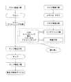
以下、本発明に係わる半導体デバイスの製造方法の実施の形態の例を説明する。図6は、本発明の半導体デバイス製造方法の実施形態の一例を示す流れ図である。この例の製造工程は以下の各工程を含む。 Hereinafter, an example of an embodiment of a semiconductor device manufacturing method according to the present invention will be described. FIG. 6 is a flowchart showing an example of the embodiment of the semiconductor device manufacturing method of the present invention. The manufacturing process of this example includes the following processes.
(1)ウエハを製造するウエハ製造工程(またはウエハを準備するウエハ準備工程)
(2)露光に使用するマスクを製作するマスク製造工程(またはマスクを準備するマスク準備工程)
(3)ウエハに必要な露光処理を行うウエハプロセッシング工程
(4)ウエハ上に形成されたチップを1個ずつ切り出し、動作可能にならしめるチップ組立工程
(5)できたチップを検査するチップ検査工程(1) Wafer manufacturing process for manufacturing a wafer (or wafer preparation process for preparing a wafer)
(2) Mask manufacturing process for manufacturing a mask to be used for exposure (or mask preparation process for preparing a mask)
(3) Wafer processing step for performing necessary exposure processing on the wafer (4) Chip assembly step for cutting out chips formed on the wafer one by one and making them operable (5) Chip inspection step for inspecting the completed chips
なお、それぞれの工程はさらにいくつかのサブ工程からなっている。 Each process further includes several sub-processes.
これらの主工程の中で、半導体デバイスの性能に決定的な影響を及ぼす主工程がウエハプロセッシング工程である。この工程では、設計された回路パターンをウエハ上に順次積層し、メモリやMPUとして動作するチップを多数形成する。このウエハプロセッシング工程は、以下の各工程を含む。 Among these main processes, the main process that has a decisive influence on the performance of the semiconductor device is the wafer processing process. In this step, designed circuit patterns are sequentially stacked on a wafer to form a large number of chips that operate as memories and MPUs. This wafer processing step includes the following steps.
(1)絶縁層となる誘電体膜や配線部、あるいは電極部を形成する金属薄膜などを形成する薄膜形成工程(CVDやスパッタリングなどを用いる)
(2)この薄膜層やウエハ基板を酸化する酸化工程
(3)薄膜層やウエハ基板などを選択的に加工するためにマスク(レクチル)を用いてレジストのパターンを形成するリソグラフィ工程
(4)レジストパターンにしたがって薄膜層や基板を加工するエッチング工程(たとえばドライエッチング技術を用いる)
(5)イオン・不純物注入拡散工程
(6)レジスト剥離工程
(7)さらに加工されたウエハを検査する検査工程(1) A thin film forming process for forming a dielectric thin film to be an insulating layer, a wiring portion, or a metal thin film for forming an electrode portion (using CVD or sputtering)
(2) Oxidation process for oxidizing the thin film layer and wafer substrate (3) Lithography process for forming a resist pattern using a mask (reticle) to selectively process the thin film layer and wafer substrate, etc. (4) Resist Etching process (for example, using dry etching technology) that processes thin film layers and substrates according to patterns
(5) Ion / impurity implantation diffusion process (6) Resist stripping process (7) Further inspection process for inspecting the processed wafer
なお、ウエハプロセッシング工程は必要な層数だけ繰り返し行い、設計通り動作する半導体デバイスを製造する。 The wafer processing process is repeated as many times as necessary to manufacture a semiconductor device that operates as designed.
本実施形態においては、上記リソグラフィ工程において、本発明によるEUV光露光装置を使用している。したがって、感応基板(ウエハ)におけるフレアによる露光量のばらつきが低減されるので、露光精度を向上させることができる。そのため、線幅の均一なデバイスを製造する事が可能となり、性能の安定したデバイスを製造する事が可能である。 In the present embodiment, the EUV light exposure apparatus according to the present invention is used in the lithography process. Therefore, variation in exposure amount due to flare in the sensitive substrate (wafer) is reduced, so that exposure accuracy can be improved. Therefore, it is possible to manufacture a device with a uniform line width, and it is possible to manufacture a device with stable performance.
本実施形態による露光装置によれば、第2の光学系を使用して、フレアの影響を考慮して露光精度を向上させることができる。 According to the exposure apparatus according to the present embodiment, the second optical system can be used to improve the exposure accuracy in consideration of the influence of flare.
本実施形態によれば、第2の光学系を使用して、露光光と異なる波長の光を、感応基板上の、露光光の照射領域に重ねて照射することにより、フレアの影響を考慮して露光精度を向上させることができる。 According to this embodiment, the influence of flare is taken into account by using the second optical system to irradiate light having a wavelength different from that of the exposure light on the exposure light irradiation region on the sensitive substrate. Exposure accuracy can be improved.
本実施形態によれば、露光装置のスループットを維持しながら、効率的にフレアの影響を考慮して露光精度を向上させることができる。 According to the present embodiment, it is possible to improve the exposure accuracy while efficiently considering the influence of flare while maintaining the throughput of the exposure apparatus.
第2の光学系が、前記第1の光学系の、前記感応基板にもっとも近い光学素子と前記感応基板との間から、前記異なる波長の光を照射するようにすれば、露光装置の既存の投影光学系の設計を変更することなく第2の光学系を設置することができる。 If the second optical system irradiates light of the different wavelength from between the optical element closest to the sensitive substrate and the sensitive substrate of the first optical system, the existing exposure apparatus can be used. The second optical system can be installed without changing the design of the projection optical system.
異なる波長の照射量を制御する照射量制御装置をさらに備えれば、照射量制御装置により第2の光学系の、露光光と異なる波長の光の照射量を制御して、フレアの影響を考慮して露光精度を向上させることができる。 If a dose control device for controlling the dose of different wavelengths is further provided, the dose control device controls the dose of light having a wavelength different from the exposure light of the second optical system to take into account the effects of flare. Thus, the exposure accuracy can be improved.
照射量制御装置が、レチクルのパターンに基づいて前記異なる波長の照射量を制御すれば、レチクルのパターンに基づくフレアの影響を考慮して露光精度を向上させることができる。 If the dose control device controls the doses of the different wavelengths based on the reticle pattern, the exposure accuracy can be improved in consideration of the influence of flare based on the reticle pattern.
照射量制御装置が、感応基板上の照射位置に基づいて前記異なる波長の照射量を制御すれば、感応基板上の照射位置に基づくフレアの影響を考慮して露光精度を向上させることができる。 If the irradiation amount control device controls the irradiation amounts of the different wavelengths based on the irradiation position on the sensitive substrate, the exposure accuracy can be improved in consideration of the influence of flare based on the irradiation position on the sensitive substrate.
101…第2の光学系、103…照射量制御装置、201…レチクルステージ、203…レチクル、301…投影光学系(第1の光学系)、401…ウエハステージ、403…ウエハ、501…制御装置DESCRIPTION OF
Claims (18)
Translated fromJapanese前記感応基板が所定の感度を有する、前記EUV光とは異なる波長の光を射出する光源を備え、前記異なる波長の光を前記感応基板に照射する第2の光学系と、
を備えたことを特徴とするEUV露光装置。A first optical system that includes a light source that emits EUV light and that exposes a sensitive substrate with EUV light;
A second optical system having a light source that emits light having a wavelength different from that of the EUV light, wherein the sensitive substrate has a predetermined sensitivity, and irradiating the sensitive substrate with light having a different wavelength;
An EUV exposure apparatus comprising:
フレア量を感応基板上の各位置において実質的に一様とするために必要な露光光とは異なる波長の光の照射量を定め、
前記異なる波長の光を前記感応基板に照射することを含むEUV露光方法。An EUV exposure method in which an exposure pattern formed on a reticle by irradiating light onto the reticle is exposed and transferred onto a sensitive substrate,
Determine the amount of light with a wavelength different from the exposure light necessary to make the flare amount substantially uniform at each position on the sensitive substrate,
An EUV exposure method comprising irradiating the sensitive substrate with light of different wavelengths.
前記感応基板に照射される露光量を調整する露光量調整光を射出する光源を備え、前記露光量調整光を前記感応基板の露光光が照射される位置と実質的に同じ位置に照射する第2の光学系と、
を備えたことを特徴とする露光装置。A first optical system that includes a light source that emits exposure light and that exposes the sensitive substrate with the exposure light;
A light source that emits an exposure adjustment light that adjusts an exposure amount applied to the sensitive substrate, and the exposure amount adjustment light is applied to substantially the same position as the exposure light of the sensitive substrate. Two optical systems;
An exposure apparatus comprising:
Priority Applications (1)
| Application Number | Priority Date | Filing Date | Title |
|---|---|---|---|
| JP2007004812AJP2008172086A (en) | 2007-01-12 | 2007-01-12 | Exposure apparatus and exposure method |
Applications Claiming Priority (1)
| Application Number | Priority Date | Filing Date | Title |
|---|---|---|---|
| JP2007004812AJP2008172086A (en) | 2007-01-12 | 2007-01-12 | Exposure apparatus and exposure method |
Publications (1)
| Publication Number | Publication Date |
|---|---|
| JP2008172086Atrue JP2008172086A (en) | 2008-07-24 |
Family
ID=39699888
Family Applications (1)
| Application Number | Title | Priority Date | Filing Date |
|---|---|---|---|
| JP2007004812APendingJP2008172086A (en) | 2007-01-12 | 2007-01-12 | Exposure apparatus and exposure method |
Country Status (1)
| Country | Link |
|---|---|
| JP (1) | JP2008172086A (en) |
Cited By (1)
| Publication number | Priority date | Publication date | Assignee | Title |
|---|---|---|---|---|
| US20140327894A1 (en)* | 2013-05-06 | 2014-11-06 | Cha-Won Koh | Lithography apparatus having effective thermal electron enhancement unit and method of forming pattern using the same |
- 2007
- 2007-01-12JPJP2007004812Apatent/JP2008172086A/enactivePending
Cited By (2)
| Publication number | Priority date | Publication date | Assignee | Title |
|---|---|---|---|---|
| US20140327894A1 (en)* | 2013-05-06 | 2014-11-06 | Cha-Won Koh | Lithography apparatus having effective thermal electron enhancement unit and method of forming pattern using the same |
| US9482953B2 (en)* | 2013-05-06 | 2016-11-01 | Samsung Electronics Co., Ltd. | Lithography apparatus having effective thermal electron enhancement unit and method of forming pattern using the same |
Similar Documents
| Publication | Publication Date | Title |
|---|---|---|
| JP4703594B2 (en) | Substrate alignment and exposure method | |
| KR100961686B1 (en) | How to perform model-based scanner tuning | |
| TWI616724B (en) | Lithographic apparatus and device manufacturing method | |
| JP4787282B2 (en) | Device manufacturing method, computer program, and lithographic apparatus | |
| JP4057847B2 (en) | Lithographic projection apparatus calibration method, patterning apparatus, and device manufacturing method | |
| JP5068844B2 (en) | Lithographic method and lithographic apparatus | |
| JP2008004937A (en) | Method and computer program for reducing wavefront aberration | |
| JP3766041B2 (en) | Lithographic apparatus, device manufacturing method, device manufactured by this method, reflector manufacturing method, reflector manufactured by this method, phase shift mask | |
| US11467509B2 (en) | Lithography process monitoring method | |
| KR102063229B1 (en) | Simulation of Lithography Using Multi-Sampling of Angle Distribution of Source Radiation | |
| US8542342B2 (en) | Method of manufacturing a miniaturized device | |
| TWI623822B (en) | Method and computer program for inspecting a substrate | |
| TW201837613A (en) | Methods of guiding process models and inspection in a manufacturing process | |
| US20240385545A1 (en) | Lithography process monitoring method | |
| JP2008283178A (en) | Lithographic apparatus and method | |
| JP2008117866A (en) | Exposure apparatus, reticle for exposure apparatus, exposure method, and device manufacturing method | |
| JP4567658B2 (en) | Device manufacturing method and computer program product | |
| JP4848229B2 (en) | Lithographic apparatus and device manufacturing method | |
| JP2006114914A (en) | Lithographic system, method for adjusting transmission characteristics of an optical path in a lithographic system, semiconductor device, method for manufacturing a reflective element for use in a lithographic system, and reflective element manufactured thereby | |
| JP2008172086A (en) | Exposure apparatus and exposure method | |
| JP2009278091A (en) | Lithography method | |
| US20240152046A1 (en) | Method of controlling semiconductor process and semiconductor processing apparatus | |
| TWI836599B (en) | Method of determining a metrology contribution from statistically independent sources, method of determining a parameter of interest of a lithographic process, and related computer program and non-transient computer program carrier | |
| JP4418782B2 (en) | Lithographic apparatus, device manufacturing method, calibration method, and computer program product | |
| JP7152597B2 (en) | Method and Apparatus for Setting Spatial Dimensions of a Scanning Beam |